KR100737732B1 - Packaging structure of MEMS microphone - Google Patents
Packaging structure of MEMS microphoneDownload PDFInfo
- Publication number
- KR100737732B1 KR100737732B1KR1020060036291AKR20060036291AKR100737732B1KR 100737732 B1KR100737732 B1KR 100737732B1KR 1020060036291 AKR1020060036291 AKR 1020060036291AKR 20060036291 AKR20060036291 AKR 20060036291AKR 100737732 B1KR100737732 B1KR 100737732B1
- Authority
- KR
- South Korea
- Prior art keywords
- case
- region
- packaging structure
- mems microphone
- sound hole
- Prior art date
- Legal status (The legal status is an assumption and is not a legal conclusion. Google has not performed a legal analysis and makes no representation as to the accuracy of the status listed.)
- Expired - Fee Related
Links
Images


Classifications
- H—ELECTRICITY
- H04—ELECTRIC COMMUNICATION TECHNIQUE
- H04R—LOUDSPEAKERS, MICROPHONES, GRAMOPHONE PICK-UPS OR LIKE ACOUSTIC ELECTROMECHANICAL TRANSDUCERS; DEAF-AID SETS; PUBLIC ADDRESS SYSTEMS
- H04R1/00—Details of transducers, loudspeakers or microphones
- H04R1/02—Casings; Cabinets ; Supports therefor; Mountings therein
- H04R1/04—Structural association of microphone with electric circuitry therefor
- H—ELECTRICITY
- H04—ELECTRIC COMMUNICATION TECHNIQUE
- H04R—LOUDSPEAKERS, MICROPHONES, GRAMOPHONE PICK-UPS OR LIKE ACOUSTIC ELECTROMECHANICAL TRANSDUCERS; DEAF-AID SETS; PUBLIC ADDRESS SYSTEMS
- H04R19/00—Electrostatic transducers
- H04R19/005—Electrostatic transducers using semiconductor materials
- H—ELECTRICITY
- H04—ELECTRIC COMMUNICATION TECHNIQUE
- H04R—LOUDSPEAKERS, MICROPHONES, GRAMOPHONE PICK-UPS OR LIKE ACOUSTIC ELECTROMECHANICAL TRANSDUCERS; DEAF-AID SETS; PUBLIC ADDRESS SYSTEMS
- H04R1/00—Details of transducers, loudspeakers or microphones
- H04R1/02—Casings; Cabinets ; Supports therefor; Mountings therein
- H04R1/021—Casings; Cabinets ; Supports therefor; Mountings therein incorporating only one transducer
- H—ELECTRICITY
- H04—ELECTRIC COMMUNICATION TECHNIQUE
- H04R—LOUDSPEAKERS, MICROPHONES, GRAMOPHONE PICK-UPS OR LIKE ACOUSTIC ELECTROMECHANICAL TRANSDUCERS; DEAF-AID SETS; PUBLIC ADDRESS SYSTEMS
- H04R1/00—Details of transducers, loudspeakers or microphones
- H04R1/08—Mouthpieces; Microphones; Attachments therefor
- H—ELECTRICITY
- H04—ELECTRIC COMMUNICATION TECHNIQUE
- H04R—LOUDSPEAKERS, MICROPHONES, GRAMOPHONE PICK-UPS OR LIKE ACOUSTIC ELECTROMECHANICAL TRANSDUCERS; DEAF-AID SETS; PUBLIC ADDRESS SYSTEMS
- H04R19/00—Electrostatic transducers
- H04R19/04—Microphones
- H—ELECTRICITY
- H04—ELECTRIC COMMUNICATION TECHNIQUE
- H04R—LOUDSPEAKERS, MICROPHONES, GRAMOPHONE PICK-UPS OR LIKE ACOUSTIC ELECTROMECHANICAL TRANSDUCERS; DEAF-AID SETS; PUBLIC ADDRESS SYSTEMS
- H04R2201/00—Details of transducers, loudspeakers or microphones covered by H04R1/00 but not provided for in any of its subgroups
- H04R2201/003—Mems transducers or their use
- H—ELECTRICITY
- H04—ELECTRIC COMMUNICATION TECHNIQUE
- H04R—LOUDSPEAKERS, MICROPHONES, GRAMOPHONE PICK-UPS OR LIKE ACOUSTIC ELECTROMECHANICAL TRANSDUCERS; DEAF-AID SETS; PUBLIC ADDRESS SYSTEMS
- H04R2201/00—Details of transducers, loudspeakers or microphones covered by H04R1/00 but not provided for in any of its subgroups
- H04R2201/02—Details casings, cabinets or mounting therein for transducers covered by H04R1/02 but not provided for in any of its subgroups
- H04R2201/029—Manufacturing aspects of enclosures transducers
- H—ELECTRICITY
- H04—ELECTRIC COMMUNICATION TECHNIQUE
- H04R—LOUDSPEAKERS, MICROPHONES, GRAMOPHONE PICK-UPS OR LIKE ACOUSTIC ELECTROMECHANICAL TRANSDUCERS; DEAF-AID SETS; PUBLIC ADDRESS SYSTEMS
- H04R2499/00—Aspects covered by H04R or H04S not otherwise provided for in their subgroups
- H04R2499/10—General applications
- H04R2499/11—Transducers incorporated or for use in hand-held devices, e.g. mobile phones, PDA's, camera's
- H—ELECTRICITY
- H05—ELECTRIC TECHNIQUES NOT OTHERWISE PROVIDED FOR
- H05K—PRINTED CIRCUITS; CASINGS OR CONSTRUCTIONAL DETAILS OF ELECTRIC APPARATUS; MANUFACTURE OF ASSEMBLAGES OF ELECTRICAL COMPONENTS
- H05K1/00—Printed circuits
- H05K1/18—Printed circuits structurally associated with non-printed electric components
- H05K1/189—Printed circuits structurally associated with non-printed electric components characterised by the use of a flexible or folded printed circuit
Landscapes
- Physics & Mathematics (AREA)
- Engineering & Computer Science (AREA)
- Acoustics & Sound (AREA)
- Signal Processing (AREA)
- Electrostatic, Electromagnetic, Magneto- Strictive, And Variable-Resistance Transducers (AREA)
- Micromachines (AREA)
- Pressure Sensors (AREA)
Abstract
Translated fromKoreanDescription
Translated fromKorean도 1은 본 발명의 실시예에 따른 멤스 마이크로폰의 패키징 구조의 분해 사시도.1 is an exploded perspective view of a packaging structure of a MEMS microphone according to an embodiment of the present invention.
도 2a 및 도 2b는 본 발명의 실시예에 따른 멤스 마이크로폰의 패키징 구조의 결합 사시도.2A and 2B are perspective views of a packaging structure of a MEMS microphone according to an exemplary embodiment of the present invention.
도 3은 본 발명의 실시예에 따른 멤스 마이크로폰의 패키징 구조의 조립 단면도.Figure 3 is an assembled cross-sectional view of the packaging structure of the MEMS microphone according to an embodiment of the present invention.
도 4는 도 1에 도시된 연성인쇄회로기판을 나타낸 도면.4 is a diagram illustrating the flexible printed circuit board of FIG. 1.
도 5는 본 발명의 다른 실시예에 따른 멤스 마이크로폰의 패키징 구조의 분해 사시도.5 is an exploded perspective view of a packaging structure of a MEMS microphone according to another embodiment of the present invention.
도 6a 및 도 6b는 본 발명의 다른 실시예에 따른 멤스 마이크로폰의 패키징 구조의 결합 사시도.6A and 6B are combined perspective views of a packaging structure of a MEMS microphone according to another embodiment of the present invention.
도 7은 본 발명의 다른 실시예에 따른 멤스 마이크로폰의 패키징 구조의 조립 단면도.Figure 7 is an assembled cross-sectional view of the packaging structure of the MEMS microphone according to another embodiment of the present invention.
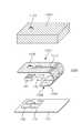
도 8a 및 도 8b는 본 발명의 실시예에 따른 멤스 마이크로폰의 패키징 구조의 다양한 형태를 도시한 예시도.8A and 8B are exemplary views showing various forms of a packaging structure of a MEMS microphone according to an embodiment of the present invention.
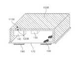
< 도면의 주요 부분에 대한 부호의 설명 > <Description of Symbols for Main Parts of Drawings>
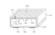
제 1 케이스 : 100 음공 : 110 1st case: 100 Sound Holes: 110
연성인쇄회로기판: 120A 트랜스듀서: 140 Flexible Printed Circuit Board: 120A Transducer: 140
증폭기 : 150 제 2 케이스 : 160 Amplifier: 150 Second Case: 160
인쇄회로기판 : 170 Printed Circuit Board: 170
본 발명은 마이크로폰의 패키징 구조에 관한 것으로, 특히 연성인쇄회로기판을 이용하여 케이스와 트랜스듀서 간의 이격거리를 감소시키는 멤스 마이크로폰의 패키징 구조에 관한 것이다.The present invention relates to a packaging structure of a microphone, and more particularly to a packaging structure of a MEMS microphone using a flexible printed circuit board to reduce the separation distance between the case and the transducer.
최근들어, 첨단 전자제품은 그 어느 때보다도 고 집적화와 고 정밀화가 이루어지고 있다. 이러한 추세에 따라, 첨단전자제품을 구성하는 부품 또한 고 집적화와 고 정밀화가 되어가고 있다. 따라서, 휴대폰이나 무전기 등에 삽입되는 마이크로폰은 제품의 경량화 및 소형화를 위하여 그 크기가 비약적으로 소형화되어 가고 있다. 이러한 마이크로폰의 소형화를 위하여 멤스(Micro Electro Mechanical System/MEMS) 기술을 적용하여 초소형의 소자를 구현할 수 있는 멤스 마이크로폰의 개발이 집중적으로 이루어지고 있다.In recent years, advanced electronic products have been more integrated and more precise than ever. According to this trend, the components that make up advanced electronic products are also becoming highly integrated and highly precise. Accordingly, microphones inserted into mobile phones or walkie-talkies have been dramatically downsized in size in order to reduce weight and size of products. For miniaturization of such microphones, the development of MEMS microphones that can realize micro devices by applying MEMS (Micro Electro Mechanical System / MEMS) technology has been intensively made.
이를 자세히 하면, 멤스 기술은 반도체 공정 특히, 집적회로 기술을 응용한 마이크로머시닝 기술을 이용하여 마이크로 단위의 초소형 센서나 액츄에이터 및 전기 기계적 구조물을 제작하는데 일반적으로 응용된다. 이러한 멤스 기술이 적용된 멤스 마이크로폰은 초소형의 소자를 구현할 수 있을 뿐만 아니라 하나의 실리콘 웨이퍼 상에서 복수개의 멤스 마이크로폰을 제조할 수 있어 멤스 마이크로폰의 대량생산이 가능하다.In detail, MEMS technology is generally applied to fabricate micro sensors, actuators and electromechanical structures in micro units using semiconductor processing, in particular, micromachining technology using integrated circuit technology. The MEMS microphone applied with the MEMS technology not only realizes a very small device but also can manufacture a plurality of MEMS microphones on a single silicon wafer, thereby enabling mass production of MEMS microphones.
멤스 마이크로폰은 일측이 개구되고 타측에 음공이 형성된 케이스, 멤스 기술로 제조되며 음성신호를 전기신호로 변환하는 트랜스듀서, 증폭기 및 트랜스듀서와 증폭기가 표면에 실장되고 케이스의 개구부를 밀폐하는 인쇄회로기판을 포함하여 구성된다.MEMS microphone is a case with one side opening and a sound hole on the other side, manufactured by MEMS technology, a transducer for converting a voice signal into an electrical signal, an amplifier, and a printed circuit board on which a transducer and an amplifier are mounted on the surface and sealing the opening of the case. It is configured to include.
여기서, 케이스에 형성된 음공과 트랜스듀서 간의 거리는 작을수록 음성신호가 효율적으로 전기신호로 변환될 수 있다. 그러나, 케이스는 금속성 재질이고, 트랜스듀서는 실리콘의 재질이기 때문에 케이스와 트랜스듀서는 직접적인 접착이 불가능하여 음공과 트랜스듀서 간의 이격거리가 발생하게 된다. 이로 인해, 멤스 마이크로폰은 저역에서 특성이 일정하지 못하여 멤스 마이크로폰의 감도가 떨어지는 현상이 발생한다.Here, as the distance between the sound hole and the transducer formed in the case is smaller, the voice signal may be efficiently converted into an electric signal. However, since the case is made of a metallic material and the transducer is made of silicon, the case and the transducer cannot be directly bonded to each other, and thus a separation distance between the sound hole and the transducer occurs. As a result, the characteristics of the MEMS microphones are not constant at low frequencies, resulting in a decrease in the sensitivity of the MEMS microphones.
본 발명의 목적은 상기의 문제를 해결하기 위한 것으로, 연성인쇄회로기판을 케이스 내측면에 부착하고 케이스에 형성된 음공과 대향되도록 연성인쇄회로기판에 트랜스듀서를 실장함으로써, 음공과 트랜스듀서 간의 이격거리를 감소시킬 수 있는 멤스 마이크로폰의 패키징 구조를 제공하는데 있다.An object of the present invention is to solve the above problems, by attaching the flexible printed circuit board to the inner surface of the case and mounting the transducer on the flexible printed circuit board to face the sound hole formed in the case, the separation distance between the sound hole and the transducer To provide a packaging structure of the MEMS microphone that can reduce the.
본 발명의 다른 목적은, 케이스에 형성된 음공과 트랜스듀서 간의 이격거리가 감소됨으로써, 음공을 통해 유입된 음성신호를 전기신호로 변환하는 효율을 증가시킬 수 있는 멤스 마이크로폰의 패키징 구조를 제공하는데 있다.Another object of the present invention is to provide a packaging structure of MEMS microphones which can increase the efficiency of converting the voice signal introduced through the sound hole into the electrical signal by reducing the separation distance between the sound hole and the transducer formed in the case.
본 발명의 다른 목적은, 케이스에 형성된 음공과 트랜스듀서 간의 이격거리가 감소됨으로써, 저역에서 실리콘 마이크로폰의 특성을 개선시킬 수 있는 멤스 마이크로폰의 패키징 구조를 제공하는데 있다.Another object of the present invention is to provide a packaging structure of MEMS microphones that can improve the characteristics of the silicon microphone at low frequencies by reducing the separation distance between the sound holes formed in the case and the transducer.
마지막으로, 본 발명의 목적은, 제 2 케이스를 이용하여 제 1 케이스의 개구부를 밀폐함과 아울러 제 1 케이스를 수납한 제 2 케이스의 끝단을 커링함으로써 제 1 케이스와 제 2 케이스의 결합력을 증가시킬 수 있는 멤스 마이크로폰의 패키징 구조를 제공하는데 있다.Finally, an object of the present invention is to increase the coupling force between the first case and the second case by sealing the opening of the first case using the second case and curing the end of the second case containing the first case. The present invention provides a packaging structure of MEMS microphones.
상기한 목적을 달성하기 위하여, 본 발명의 실시예에 따른 실리콘 마이크로폰 패키징구조는, 일측이 개구되고, 타측에 음공이 형성된 제 1 케이스; 상기 제 1 케이스 내측면에 부착되며 상기 음공에 대향되도록 홀이 형성된 제 1 영역, 외부기기로 전기신호를 전달하는 제 1 전극을 구비하는 제 2 영역 및 상기 제 1 영역과 상기 제 2 영역을 연결하는 연결부를 포함하여 구성되는 연성인쇄회로기판; 상기 제 1 영역의 저면에 상기 홀 및 상기 음공에 대향하도록 실장되는 트랜스듀서 및 상기 제 1 영역의 저면에 실장되는 증폭기; 및 상기 제 1 케이스의 개구부를 밀폐하며 상기 연장부 및 제 2 영역이 외부로 연장되도록 하는 연장슬롯이 형성되는 제 2 케이스;를 구비하는 것을 특징으로 한다.In order to achieve the above object, the silicon microphone packaging structure according to an embodiment of the present invention, one side is opened, the first case is formed with sound holes on the other side; A first area attached to an inner surface of the first case and having a hole facing the sound hole, a second area having a first electrode for transmitting an electrical signal to an external device, and connecting the first area and the second area; A flexible printed circuit board configured to include a connection portion; A transducer mounted on the bottom of the first region so as to face the hole and the sound hole and an amplifier mounted on the bottom of the first region; And a second case sealing the opening of the first case and having an extension slot for extending the extension and the second region to the outside.
상기 제 1 케이스는 상기 연성인쇄회로기판 중 일부가 외부로 연장되도록 상기 연장슬롯과 대향되는 상기 제 1 케이스의 외주면에 홈을 구비하는 것을 특징으로 한다.The first case may be provided with a groove on an outer circumferential surface of the first case facing the extension slot such that a part of the flexible printed circuit board extends to the outside.
상기 연장부 및 제 2 영역은 상기 연장슬롯과 상기 홈에 의해 형성된 통로를 통하여 외부로 연장되는 것을 특징으로 하는 멤스 마이크로폰의 패키징 구조.Wherein said extension portion and said second region extend outwardly through a passage formed by said extension slot and said groove.
본 발명의 실시예에 따른 실리콘 마이크로폰 패키징구조는, 일측이 개구되고, 타측에 음공이 형성된 제 1 케이스; 상기 제 1 케이스 내측면에 부착되며 상기 음공에 대향되도록 홀이 형성된 제 1 영역, 상기 제 1 영역과 연결되며 인쇄회로기판 일면에 접착되는 제 2 영역을 포함하여 구성되는 연성인쇄회로기판; 상기 제 1 영역의 저면에 상기 홀 및 상기 음공에 대향하도록 실장되는 트랜스듀서 및 상기 제 1 영역의 저면에 실장되는 증폭기; 및 상기 제 1 케이스의 개구부를 밀폐하며 상기 제 2 영역과 접촉하는 인쇄회로기판;을 구비하는 것을 특징으로 한다.Silicon microphone packaging structure according to an embodiment of the present invention, one side is opened, the first case has a sound hole on the other side; A flexible printed circuit board attached to the inner surface of the first case and including a first region having a hole facing the sound hole, and a second region connected to the first region and bonded to one surface of the printed circuit board; A transducer mounted on the bottom of the first region so as to face the hole and the sound hole and an amplifier mounted on the bottom of the first region; And a printed circuit board sealing the opening of the first case and contacting the second area.
상술한 목적 및 기타의 목적과 본 발명의 특징 및 이점은 첨부된 도면과 관련한 다음의 상세한 설명을 통하여 보다 분명해 질 것이다. 이하, 첨부된 도면을 참조하여 본 발명의 실시예를 상세히 설명하면 다음과 같다.The above and other objects and features and advantages of the present invention will become more apparent from the following detailed description taken in conjunction with the accompanying drawings. Hereinafter, exemplary embodiments of the present invention will be described in detail with reference to the accompanying drawings.
도 1은 본 발명의 실시예에 따른 멤스 마이크로폰의 패키징 구조의 분해 사시도이고, 도 2a 및 도 2b는 본 발명의 실시예에 따른 멤스 마이크로폰의 패키징 구조의 결합 사시도이며, 도 3은 본 발명의 실시예에 따른 멤스 마이크로폰의 패키 징 구조의 조립 단면도이다.1 is an exploded perspective view of a packaging structure of a MEMS microphone according to an embodiment of the present invention, and FIGS. 2A and 2B are combined perspective views of a packaging structure of a MEMS microphone according to an embodiment of the present invention, and FIG. 3 is an embodiment of the present invention. Assembled sectional view of the packaging structure of a MEMS microphone according to an example.
도 1 내지 도 3을 참조하면, 본 발명의 실시예에 따른 멤스 마이크로폰의 패키징 구조는 일측이 개구되며, 개구부에 대향되는 면에 음공(110A)이 형성된 제 1 케이스(100A), 제 1 케이스(100A)의 내측면 중 음공(110A)이 형성된 면을 포함한 적어도 하나의 면과 일부분 접착되는 연성인쇄회로기판(Flexible Printed Circuit Board 이하 FPCB)(120A), 음공(110A)과 대향되도록 FPCB(120A)에 실장되는 트랜스듀서(140)와 증폭기(150) 및 제 1 케이스(100A)의 개구부를 밀폐하는 제 2 케이스(160)로 구성된다.1 to 3, the packaging structure of a MEMS microphone according to an exemplary embodiment of the present invention has a
여기서, FPCB(120A)는 제 1 케이스(100A) 내측면에 부착되며 음공(110A)에 대향되도록 트랜스듀서(140) 및 증폭기(150)가 실장되는 제 1 영역(122A), 외부기기로 전기신호를 전달하는 제 1 전극(135)을 구비하며 제 2 케이스(160)의 일면과 접착되는 제 2 영역(126A), 제 1 영역(122A)과 제 2 영역(126A)을 연결하는 연결부(124A)를 포함하여 구성된다. 이러한 FPCB(120A)의 상세한 설명은 후술하기로 한다.Here, the FPCB 120A is attached to the inner surface of the
제 1 케이스(100A)는 일측이 개구되고, 개구부에 대향되는 면에 음공(110A)이 형성된다. 또한, 제 1 케이스(100A)의 일측면에 홈(115A)이 형성되는데, 이 홈(115A)은 연결부(124A)가 제 2 케이스(160)에 형성된 연장슬롯(165)에 도달할 수 있는 경로를 제공한다. 이러한 제 1 케이스(100A)는 노이즈 차단특성이 우수한 니켈, 동, 알루미늄, 구리 등의 도전재질 또는 이들의 합금으로 형성될 수 있다.One side of the
트랜스듀서(140)는 음공(110A)과 대향되도록 제 1 영역(122A)에 형성된 홀(125A)에 적층되어 음공(110A)을 통해 유입된 음성신호를 전기신호로 변환한다. 이러한 트랜스듀서(140)는 실리콘 웨이퍼에 반도체 공정, 특히 집적회로 기술을 응용한 마이크로머시닝 기술을 이용하여 마이크로 단위의 초소형 전기 기계적 구조물이 생산가능한 멤스 기술을 적용하여 제작된다. 이렇게 제작된 트랜스듀서(140)는 통상적으로 진동판이라 일컫는 실리콘 멤브레인 및 반영구적인 전하를 가지는 배극판을 형성한다.The
증폭기(150)는 제 1 영역(122A)에 실장되어 트랜스듀서(140)에서 생성된 전기신호를 전송받아 증폭하여 제 1 영역(122A)에 형성된 제 1 회로패턴(131A)에 증폭된 전기신호를 인가한다.The
제 2 케이스(160)는 일측이 개구되고, 외주면에는 제 1 케이스(100A)에 형성된 홈(115A)과 대향되로록 연장슬롯(165)이 형성된다. 이러한 제 2 케이스(160)는 개구부를 통해 FPCB(120A)의 제 1 영역(122A), 트랜스듀서(140), 증폭기(150) 및 제 1 케이스(100A)를 수납하고, 개구부 끝단을 커링(Curling)함으로써, 제 1 케이스(100A)와 제 2 케이스(160) 사이의 갭(Gap)을 방지하여 전기적인 밀착을 유도하고, 트랜스듀서(140) 및 증폭기(150)가 실장된 제 1 영역(122A)를 외부의 충격으로부터 보호함과 아울러, 외부 전자 노이즈(Noise)를 차폐한다.One side of the
또한, 연장슬롯(165)에는 연결부(124A)가 배치되고, 연장슬롯(165)은 연결부(124A)가 배치된 영역을 제외하고 에폭시를 이용하여 실링(Sealing)되므로써 연장슬롯(165)을 통해 유입되는 먼지 및 노이즈를 차단할 수 있다. 제 2 케이스(160)는 제 1 케이스(100A)와 마찬가지로 노이즈 차단특성이 우수한 니켈, 동, 알루미늄, 구리 등의 도전재질 또는 이들의 합금으로 형성될 수 있다. In addition, the
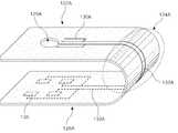
4는 도 1 에 도시된 본 발명의 실시예에 따른 FPCB(120A)의 사시도이다.4 is a perspective view of the FPCB 120A according to the embodiment of the present invention shown in FIG.
도 4를 참조하면, FPCB(120A)는 상술한 바와 같이 제 1 영역(122A), 제 2 영역(126A) 및 연결부(124A)로 구성된다. 그리고, 제 1 영역(122A)의 표면에는 SMT(Surface Mount Technology 표면 실장 기술)을 이용하여 트랜스듀서(140) 및 증폭기(150)가 실장된다.Referring to FIG. 4, the FPCB 120A includes a
이를 자세히 하면, 제 1 영역(122A)은 제 1 케이스(100A) 내측면 중 음공(110A)이 형성된 내측면을 포함한 적어도 하나의 내측면과 접착된다. 이러한, 제 1 영역(122A)에는 홀(125A) 및 제 1 회로패턴(131A)이 형성되는데, 홀(125A)에는 음공(110A)과 대향되도록 트랜스듀서(140)가 실장된다. 제 1 회로패턴(131A)은 트랜스듀서(140)에서 생성된 전기 신호를 트랜스듀서(140) 일측에 배치된 증폭기(150)에 전달하고, 증폭기(150)를 거친 전기신호를 연결부(124A)에 형성된 제 2 회로패턴(132A)에 전달한다.In detail, the
연결부(124A)는 제 1 케이스(100A)에 형성된 홈(115A) 및 제 2 케이스(160)에 형성된 연장슬롯(165) 즉, 통로에 배치된다. 연결부(124A)에는 제 2 회로패턴(132A)이 형성되어 제 1 회로패턴(131A)으로부터 전기신호를 전달받아 제 2 영역(126A)의 제 3 회로패턴(133A)으로 전달한다.The
제 2 영역(126A)은 제 1 케이스(100A)의 개구부를 밀폐하는 제 2 케이스(160)의 배면에 접착된다. 제 2 영역(126A)에는 제 3 회로패턴(133A) 및 제 1 전극(135)이 형성되는데 제 3 회로패턴(133A)은 제 2 회로패턴(132A)으로부터 전달 받은 전기신호를 제 1 전극(135)으로 전달하고, 제 1 전극(135)은 제 3 회로패턴(133A)으로부터 전달받은 전기신호를 외부기기에 전달한다.The
이러한 FPCB(120A)는 CCL(Copper Clad Laminate)이라고도 불리는 동박 적층판으로 구성된다. 동박 적층판은 굴곡성과 내열성이 뛰어난 폴리이미드 필름이나 폴리에스테르와 같은 절연재의 양면에 접착층을 형성하여 굴곡성과 인장성이 뛰어난 구리(Cu)를 입힌 얇은 적층판이며, 동박층 형성 후 동박패턴을 보호하기 위해 Cover-Lay층을 형성하기도 한다. 이렇게 형성된 FPCB(120A)는 접착제, 용융 및 씰링(sealing) 중 적어도 하나를 이용하여 제 1 케이스(100A) 및 제 2 케이스(160)에 접착되는 것이 바람직하다. This
도 5 내지 도 7은 본 발명의 다른 실시예에 따른 실리콘 마리크로폰 패키징 구조의 분해 사시도, 결합 사시도 및 조립 단면도이다.5 to 7 is an exploded perspective view, a combined perspective view and an assembly cross-sectional view of a silicon macrophone packaging structure according to another embodiment of the present invention.
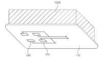
도 5 내지 도 7을 참조하면, 본 발명의 다른 실시예에 따른 멤스 마이크로폰의 패키징 구조는 일측이 개구되며 개구부에 대향되는 면에 음공(110B)이 형성된 제 1 케이스(100B), 제 1 케이스(100B)의 내측면 중에서 음공(110B)이 형성된 면을 포함하여 적어도 하나의 면과 일측이 접착되는 FPCB(120B), FPCB(120B)에 실장되는 트랜스듀서(140)와 증폭기(150) 및 제 1 케이스(100B)의 개구부를 밀폐하는 인쇄회로기판(Printed Circuit Board 이하 PCB)(170)을 구비한다.5 to 7, the packaging structure of the MEMS microphone according to another exemplary embodiment of the present invention may include a
여기서, 본 발명의 다른 실시예에 따른 멤스 마이크로폰의 패키징 구조는 본 발명의 실시예에 개시된 구성과 비교하여, 제 1 케이스(100B), FPCB(120B) 및 PCB(170)를 제외한 구성이 동일하므로 제 1 케이스(100B), FPCB(120B) 및 PCB(170) 를 제외한 구성에 대한 상세한 설명은 생략하기로 한다.Here, the packaging structure of the MEMS microphone according to another embodiment of the present invention is the same as the configuration disclosed in the embodiment of the present invention, except the
제 1 케이스(100B)는 일측이 개구되고, 개구부에 대향되는 면에 음공(110B)이 형성되고 음공(110B)이 형성된 면을 포함한 제 1 케이스(100B) 내측면 중 적어도 하나의 면은 제 1 영역(122B)과 접촉한다. 이러한 제 1 케이스(100B)는 노이즈 차단특성이 우수한 니켈, 동, 알루미늄, 구리 등의 도전재질 또는 이들의 합금으로 형성될 수 있다.At least one surface of the inner side of the
FPCB(120B)는 제 1 영역(122B) 및 제 2 영역(126B)로 구성된다. 그리고, 제 1 영역(122B)의 표면에는 SMT(Surface Mount Technology 표면 실장 기술)을 이용하여 트랜스듀서(140) 및 증폭기(150)가 실장된다.
이를 자세히 하면, 제 1 영역(122B)은 제 1 케이스(100B) 내측면 중 음공(110B)이 형성된 내측면을 포함한 적어도 하나의 내측면과 접착된다. 이러한, 제 1 영역(122B)에는 홀(125B) 및 제 1 회로패턴(131B)이 형성되는데, 홀(125B)에는 음공(110B)과 대향되도록 트랜스듀서(140)가 실장되고, 트랜스듀서(140)의 일측에는 증폭기(150)가 실장된다. 제 1 회로패턴(131B)은 트랜스듀서(140)에서 생성된 전기 신호를 트랜스듀서(140) 일측에 배치된 증폭기(150)에 전달하고, 증폭기(150)를 거친 전기신호는 제 2 영역(126B)에 형성된 제 4 회로패턴(133B)에 전달한다. 제 2 영역(126B)은 제 1 케이스(100B)의 개구부를 밀폐하는 PCB(170)의 배면에 접착된다. 제 2 영역(126)에는 제 4 회로패턴(133B)이 형성되는데 제 4 회로패턴(133B)은 제 1 회로패턴(131B)으로부터 전달받은 전기신호를 PCB(170)에 형성된 제 5 회로패턴(173)으로 전달한다.In detail, the
이러한 FPCB(120B)는 CCL(Copper Clad Laminate)이라고도 불리는 동박 적층판으로 구성된다. 동박 적층판은 굴곡성과 내열성이 뛰어난 폴리이미드 필름이나 폴리에스테르와 같은 절연재의 양면에 접착층을 형성하여 굴곡성과 인장성이 뛰어난 구리(Cu)를 입힌 얇은 적층판이며, 동박층 형성 후 동박패턴을 보호하기 위해 Cover-Lay층을 형성하기도 한다. 이렇게 형성된 FPCB(120B)는 접착제, 용융 및 씰링(sealing) 중 적어도 하나를 이용하여 제 1 케이스(100B)와 접착되는 것이 바람직하다.This
PCB(170)는 FPCB(120B)의 제 2 영역(126B)에 형성된 제 4 회로패턴(133B)으로부터 인가된 전기신호를 제 2 전극(180)으로 전달하는 제 5 회로패턴(173) 및 제 5 회로패턴(175)으로부터 전달된 전기신호를 외부기기로 전달하는 제 2 전극(180)이 형성된다.The
이러한 PCB(170)는 제 1 케이스(100B)의 개구부를 밀폐하고 제 2 영역(126B)과 안정적으로 전기적 연결을 유지하기 위하여 제 2 영역(126B)과 접촉하는 끝단에 솔더부(190)가 형성된다. 그리고, PCB(170)는 제 1 케이스(100B)와 레이저 웰딩(Laser Welding)을 이용하여 밀폐하는 것이 바람직하며, 이렇게 제 1 케이스(100B)와 PCB(170)를 밀폐함으로써 외부로부터 유입되는 먼지나 노이즈를 차단할 수 있다.The
한편, 본 발명의 실시예에 따른 멤스 마이크로폰의 패키징 구조는 사각형태를 주로 설명하고 있지만 이에 한정되는 것이 아니라 도 8a 및 도 8b에 도시된 바와 같이 실리콘 마이크로폰이 실장되는 외부장치의 형태에 따라 타원통형 또는 다 각통형 등의 다양한 형태로 수정 또는 변경이 가능할 것이다.On the other hand, the packaging structure of the MEMS microphone according to an embodiment of the present invention mainly describes a rectangular shape, but is not limited thereto, as shown in FIGS. 8A and 8B, an elliptic cylinder type according to the form of an external device in which the silicon microphone is mounted. Or it may be modified or changed in various forms, such as polygonal.
이와 같이, 본 발명의 실시예에 따른 멤스 마이크로폰의 패키징 구조에 있어서, 실리콘 마이크로폰 패키지의 각 구성요소는 다양한 변형 및 재질의 대체가 실시될 수 있으므로, 각 구성요소는 본 발명의 실시예에 따른 멤스 마이크로폰의 패키징 구조에 의해 한정되는 것은 아니다.As such, in the packaging structure of the MEMS microphone according to the embodiment of the present invention, each component of the silicon microphone package may be modified in various modifications and materials, and thus, each component may be a MEMS according to the embodiment of the present invention. It is not limited by the packaging structure of the microphone.
이상에서 설명한 바와 같이, 본 발명의 실시예에 따른 멤스 마이크로폰의 패키징 구조는, 연성인쇄회로기판을 케이스 내측면에 부착하고 케이스에 형성된 음공과 대향되도록 연성인쇄회로기판에 트랜스듀서를 실장함으로써, 음공과 트랜스듀서 간의 이격거리를 감소시킬 수 있다.As described above, the packaging structure of MEMS microphone according to an embodiment of the present invention, by attaching a flexible printed circuit board to the inner surface of the case and mounting the transducer on the flexible printed circuit board to face the sound holes formed in the case, The separation distance between the transducer and the transducer can be reduced.
본 발명의 다른 실시예에 따른 멤스 마이크로폰의 패키징 구조는, 케이스에 형성된 음공과 트랜스듀서 간의 이격거리가 감소됨으로써, 음공을 통해 유입된 음성신호를 전기신호로 변환하는 효율을 증가시킬 수 있다.The packaging structure of the MEMS microphone according to another embodiment of the present invention can reduce the separation distance between the sound hole and the transducer formed in the case, thereby increasing the efficiency of converting the voice signal introduced through the sound hole into an electrical signal.
본 발명의 다른 실시예에 따른 멤스 마이크로폰의 패키징 구조는, 케이스에 형성된 음공과 트랜스듀서 간의 이격거리가 감소됨으로써, 저역에서 실리콘 마이크로폰의 특성을 개선시킬 수 있다.The packaging structure of the MEMS microphone according to another embodiment of the present invention can reduce the separation distance between the sound hole and the transducer formed in the case, thereby improving the characteristics of the silicon microphone in the low range.
마지막으로, 본 발명의 다른 실시예에 따른 멤스 마이크로폰의 패키징 구조는, 제 2 케이스를 이용하여 제 1 케이스의 개구부를 밀폐함과 아울러 제 1 케이스를 수납한 제 2 케이스의 끝단을 커링함으로써 제 1 케이스와 제 2 케이스의 결합 력을 증가시킬 수 있다.Finally, the packaging structure of the MEMS microphone according to another embodiment of the present invention, by closing the opening of the first case by using the second case and by curing the end of the second case housing the first case The coupling force of the case and the second case can be increased.
아울러 본 발명의 바람직한 실시예들은 예시의 목적을 위해 개시된 것이며, 당업자라면 본 발명의 사상과 범위 안에서 다양한 수정, 변경, 부가 등이 가능할 것이며, 이러한 수정 변경 등은 이하의 특허청구의 범위에 속하는 것으로 보아야 할 것이다.In addition, preferred embodiments of the present invention are disclosed for the purpose of illustration, those skilled in the art will be able to make various modifications, changes, additions, etc. within the spirit and scope of the present invention, such modifications and modifications belong to the scope of the claims You will have to look.
Claims (10)
Translated fromKoreanPriority Applications (2)
| Application Number | Priority Date | Filing Date | Title |
|---|---|---|---|
| KR1020060036291AKR100737732B1 (en) | 2006-04-21 | 2006-04-21 | Packaging structure of MEMS microphone |
| PCT/KR2006/003111WO2007123293A1 (en) | 2006-04-21 | 2006-08-08 | Packaging structure of mems microphone |
Applications Claiming Priority (1)
| Application Number | Priority Date | Filing Date | Title |
|---|---|---|---|
| KR1020060036291AKR100737732B1 (en) | 2006-04-21 | 2006-04-21 | Packaging structure of MEMS microphone |
Publications (1)
| Publication Number | Publication Date |
|---|---|
| KR100737732B1true KR100737732B1 (en) | 2007-07-10 |
Family
ID=38503853
Family Applications (1)
| Application Number | Title | Priority Date | Filing Date |
|---|---|---|---|
| KR1020060036291AExpired - Fee RelatedKR100737732B1 (en) | 2006-04-21 | 2006-04-21 | Packaging structure of MEMS microphone |
Country Status (2)
| Country | Link |
|---|---|
| KR (1) | KR100737732B1 (en) |
| WO (1) | WO2007123293A1 (en) |
Cited By (5)
| Publication number | Priority date | Publication date | Assignee | Title |
|---|---|---|---|---|
| WO2010005142A1 (en)* | 2008-07-11 | 2010-01-14 | Bse Co., Ltd | A variable directional microphone assembly and method of making the microphone assembly |
| WO2010005143A1 (en)* | 2008-07-11 | 2010-01-14 | Bse Co., Ltd | A variable directional microphone assembly and method of making the microphone assembly |
| KR100982239B1 (en)* | 2007-11-02 | 2010-09-14 | 주식회사 비에스이 | MEMS microphone package with sound hole in PCB |
| CN102316402A (en)* | 2010-07-09 | 2012-01-11 | 宝星电子株式会社 | Microphone |
| KR20230154149A (en)* | 2018-01-08 | 2023-11-07 | 엘지전자 주식회사 | Refigerator |
Families Citing this family (10)
| Publication number | Priority date | Publication date | Assignee | Title |
|---|---|---|---|---|
| DE102008012913A1 (en) | 2008-03-06 | 2009-09-10 | Valeo Schalter Und Sensoren Gmbh | Electrical component or device with a flexible printed circuit board |
| JP5302867B2 (en)* | 2009-12-07 | 2013-10-02 | ホシデン株式会社 | Microphone |
| US9212052B2 (en) | 2013-08-07 | 2015-12-15 | Invensense, Inc. | Packaged microphone with multiple mounting orientations |
| KR20160110861A (en)* | 2015-03-13 | 2016-09-22 | 삼성디스플레이 주식회사 | Flexible circuit substrate and display device including the same |
| US9965000B2 (en) | 2015-04-20 | 2018-05-08 | Microsoft Technology Licensing, Llc. | Integrated protective mesh |
| CN204652665U (en)* | 2015-05-08 | 2015-09-16 | 中兴通讯股份有限公司 | Microphone hermetically-sealed construction and electronic equipment |
| CN107249149A (en)* | 2017-07-31 | 2017-10-13 | 广东欧珀移动通信有限公司 | Microphone assembly and electronic equipment |
| CN111108756B (en)* | 2017-09-29 | 2021-07-09 | 华为技术有限公司 | Microphone Components and Electronics |
| CN110958512B (en)* | 2018-09-27 | 2025-07-25 | 北京小米移动软件有限公司 | Microphone module and terminal equipment |
| CN110958506A (en)* | 2018-09-27 | 2020-04-03 | 北京小米移动软件有限公司 | Microphone module and electronic equipment |
Citations (2)
| Publication number | Priority date | Publication date | Assignee | Title |
|---|---|---|---|---|
| US6324907B1 (en) | 1999-11-29 | 2001-12-04 | Microtronic A/S | Flexible substrate transducer assembly |
| KR20040026758A (en)* | 2002-09-26 | 2004-04-01 | 삼성전자주식회사 | Manufacturing method for Flexible MEMS transducer |
Family Cites Families (2)
| Publication number | Priority date | Publication date | Assignee | Title |
|---|---|---|---|---|
| JP3472502B2 (en)* | 1999-02-17 | 2003-12-02 | ホシデン株式会社 | Semiconductor electret condenser microphone |
| JP3436205B2 (en)* | 1999-02-22 | 2003-08-11 | 株式会社村田製作所 | Piezo acoustic components |
- 2006
- 2006-04-21KRKR1020060036291Apatent/KR100737732B1/ennot_activeExpired - Fee Related
- 2006-08-08WOPCT/KR2006/003111patent/WO2007123293A1/enactiveApplication Filing
Patent Citations (2)
| Publication number | Priority date | Publication date | Assignee | Title |
|---|---|---|---|---|
| US6324907B1 (en) | 1999-11-29 | 2001-12-04 | Microtronic A/S | Flexible substrate transducer assembly |
| KR20040026758A (en)* | 2002-09-26 | 2004-04-01 | 삼성전자주식회사 | Manufacturing method for Flexible MEMS transducer |
Cited By (12)
| Publication number | Priority date | Publication date | Assignee | Title |
|---|---|---|---|---|
| KR100982239B1 (en)* | 2007-11-02 | 2010-09-14 | 주식회사 비에스이 | MEMS microphone package with sound hole in PCB |
| WO2010005142A1 (en)* | 2008-07-11 | 2010-01-14 | Bse Co., Ltd | A variable directional microphone assembly and method of making the microphone assembly |
| WO2010005143A1 (en)* | 2008-07-11 | 2010-01-14 | Bse Co., Ltd | A variable directional microphone assembly and method of making the microphone assembly |
| CN101626531B (en)* | 2008-07-11 | 2012-12-26 | 宝星电子株式会社 | A variable directional microphone assembly and method of making the microphone assembly |
| CN101626532B (en)* | 2008-07-11 | 2013-01-16 | 宝星电子株式会社 | A variable directional microphone assembly and method of making the microphone assembly |
| CN102316402A (en)* | 2010-07-09 | 2012-01-11 | 宝星电子株式会社 | Microphone |
| WO2012005434A3 (en)* | 2010-07-09 | 2012-03-01 | 주식회사 비에스이 | Microphone |
| KR101130335B1 (en) | 2010-07-09 | 2012-03-26 | 주식회사 비에스이 | microphone |
| KR20230154149A (en)* | 2018-01-08 | 2023-11-07 | 엘지전자 주식회사 | Refigerator |
| KR102726183B1 (en)* | 2018-01-08 | 2024-11-06 | 엘지전자 주식회사 | Refigerator |
| KR20240161998A (en)* | 2018-01-08 | 2024-11-14 | 엘지전자 주식회사 | Refigerator |
| KR102784031B1 (en) | 2018-01-08 | 2025-03-21 | 엘지전자 주식회사 | Refigerator |
Also Published As
| Publication number | Publication date |
|---|---|
| WO2007123293A1 (en) | 2007-11-01 |
Similar Documents
| Publication | Publication Date | Title |
|---|---|---|
| KR100737732B1 (en) | Packaging structure of MEMS microphone | |
| KR100797443B1 (en) | MEMS microphone packaging structure | |
| US8995694B2 (en) | Embedded circuit in a MEMS device | |
| CN1917720B (en) | Silicon base capacitor microphone | |
| KR100722687B1 (en) | Directional Silicon Condenser Microphone with Additional Back Chamber | |
| US8041064B2 (en) | Card type MEMS microphone | |
| US9485560B2 (en) | Embedded circuit in a MEMS device | |
| KR100737730B1 (en) | MEMS microphone packaging structure | |
| WO2012017805A1 (en) | Microphone unit | |
| US8818010B2 (en) | Microphone unit | |
| JP5022261B2 (en) | Microphone unit | |
| KR100737726B1 (en) | MEMS microphone packaging structure | |
| JP2008539657A (en) | Acoustic transducer module | |
| WO2010090070A1 (en) | Microphone unit | |
| JP4655017B2 (en) | Acoustic sensor | |
| KR100722689B1 (en) | Silicon Condenser Microphone with Additional Back Chamber | |
| JP5298384B2 (en) | Microphone unit | |
| WO2016153871A1 (en) | Embedded circuit in a mems device | |
| JP2015532548A (en) | Embedded circuit in a MEMS device | |
| CN109495831A (en) | A kind of encapsulating structure and its manufacturing method of MEMS microphone | |
| JP5065974B2 (en) | Microphone unit and manufacturing method thereof | |
| WO2007024048A1 (en) | Silicon based condenser microphone | |
| JP5402320B2 (en) | Microphone unit | |
| CN211930826U (en) | Novel microphone packaging structure | |
| KR20080101374A (en) | Condenser microphone |
Legal Events
| Date | Code | Title | Description |
|---|---|---|---|
| A201 | Request for examination | ||
| PA0109 | Patent application | St.27 status event code:A-0-1-A10-A12-nap-PA0109 | |
| PA0201 | Request for examination | St.27 status event code:A-1-2-D10-D11-exm-PA0201 | |
| D13-X000 | Search requested | St.27 status event code:A-1-2-D10-D13-srh-X000 | |
| D14-X000 | Search report completed | St.27 status event code:A-1-2-D10-D14-srh-X000 | |
| E902 | Notification of reason for refusal | ||
| PE0902 | Notice of grounds for rejection | St.27 status event code:A-1-2-D10-D21-exm-PE0902 | |
| P11-X000 | Amendment of application requested | St.27 status event code:A-2-2-P10-P11-nap-X000 | |
| P13-X000 | Application amended | St.27 status event code:A-2-2-P10-P13-nap-X000 | |
| E701 | Decision to grant or registration of patent right | ||
| PE0701 | Decision of registration | St.27 status event code:A-1-2-D10-D22-exm-PE0701 | |
| GRNT | Written decision to grant | ||
| PR0701 | Registration of establishment | St.27 status event code:A-2-4-F10-F11-exm-PR0701 | |
| PR1002 | Payment of registration fee | St.27 status event code:A-2-2-U10-U11-oth-PR1002 Fee payment year number:1 | |
| PG1601 | Publication of registration | St.27 status event code:A-4-4-Q10-Q13-nap-PG1601 | |
| R18-X000 | Changes to party contact information recorded | St.27 status event code:A-5-5-R10-R18-oth-X000 | |
| PR1001 | Payment of annual fee | St.27 status event code:A-4-4-U10-U11-oth-PR1001 Fee payment year number:4 | |
| PR1001 | Payment of annual fee | St.27 status event code:A-4-4-U10-U11-oth-PR1001 Fee payment year number:5 | |
| FPAY | Annual fee payment | Payment date:20120629 Year of fee payment:6 | |
| PR1001 | Payment of annual fee | St.27 status event code:A-4-4-U10-U11-oth-PR1001 Fee payment year number:6 | |
| FPAY | Annual fee payment | Payment date:20130731 Year of fee payment:7 | |
| PR1001 | Payment of annual fee | St.27 status event code:A-4-4-U10-U11-oth-PR1001 Fee payment year number:7 | |
| PR1001 | Payment of annual fee | St.27 status event code:A-4-4-U10-U11-oth-PR1001 Fee payment year number:8 | |
| LAPS | Lapse due to unpaid annual fee | ||
| PC1903 | Unpaid annual fee | St.27 status event code:A-4-4-U10-U13-oth-PC1903 Not in force date:20150705 Payment event data comment text:Termination Category : DEFAULT_OF_REGISTRATION_FEE | |
| P22-X000 | Classification modified | St.27 status event code:A-4-4-P10-P22-nap-X000 | |
| PC1903 | Unpaid annual fee | St.27 status event code:N-4-6-H10-H13-oth-PC1903 Ip right cessation event data comment text:Termination Category : DEFAULT_OF_REGISTRATION_FEE Not in force date:20150705 | |
| P22-X000 | Classification modified | St.27 status event code:A-4-4-P10-P22-nap-X000 | |
| PN2301 | Change of applicant | St.27 status event code:A-5-5-R10-R13-asn-PN2301 St.27 status event code:A-5-5-R10-R11-asn-PN2301 |