Movatterモバイル変換


[0]ホーム

URL:


KR100736008B1 - Display device and method of manufacturing the same - Google Patents

Display device and method of manufacturing the same
Download PDF

Info

Publication number
KR100736008B1
KR100736008B1KR1020050048068AKR20050048068AKR100736008B1KR 100736008 B1KR100736008 B1KR 100736008B1KR 1020050048068 AKR1020050048068 AKR 1020050048068AKR 20050048068 AKR20050048068 AKR 20050048068AKR 100736008 B1KR100736008 B1KR 100736008B1
Authority
KR
South Korea
Prior art keywords
light emitting
current
pixel circuit
electrode
layer
Prior art date
Legal status (The legal status is an assumption and is not a legal conclusion. Google has not performed a legal analysis and makes no representation as to the accuracy of the status listed.)
Expired - Fee Related
Application number
KR1020050048068A
Other languages
Korean (ko)
Other versions
KR20060048203A (en
Inventor
도모유키 시라사키
다다히사 도야마
마나부 다케이
준 오구라
이쿠히로 야마구치
츠요시 오자키
Original Assignee
가시오게산키 가부시키가이샤
Priority date (The priority date is an assumption and is not a legal conclusion. Google has not performed a legal analysis and makes no representation as to the accuracy of the date listed.)
Filing date
Publication date
Priority claimed from JP2004168619Aexternal-prioritypatent/JP4424078B2/en
Priority claimed from JP2004171192Aexternal-prioritypatent/JP4315058B2/en
Application filed by 가시오게산키 가부시키가이샤filedCritical가시오게산키 가부시키가이샤
Publication of KR20060048203ApublicationCriticalpatent/KR20060048203A/en
Application grantedgrantedCritical
Publication of KR100736008B1publicationCriticalpatent/KR100736008B1/en
Anticipated expirationlegal-statusCritical
Expired - Fee Relatedlegal-statusCriticalCurrent

Links

Images

Classifications

Landscapes

Abstract

Translated fromKorean

본 발명은 발광소자를 구비한 표시장치 및 제조방법에 관한 것으로,The present invention relates to a display device having a light emitting element and a manufacturing method.

전압강하나 전류지연의 발생을 억제하는 것이고, 기판과 상기 기판상에 설치된 발광소자와, 상기 발광소자를 구동하기 위한 전극을 갖는 화소회로와, 상기 화소회로에 접속되고 상기 화소회로의 전극과는 다른 층의 도전층을 갖는 배선을 구비하는 것을 특징으로 하는 표시장치이다.It is to suppress the occurrence of voltage drop or current delay, and includes a pixel circuit having a substrate and a light emitting element provided on the substrate, an electrode for driving the light emitting element, and a pixel circuit connected to the pixel circuit and different from the electrode of the pixel circuit. A display device comprising a wiring having a conductive layer of a layer.

트랜지스터어레이기판, 일렉트로루미네선트 디스플레이패널, 화소회로, EL라인, 유기EL소자, 전류원라인Transistor array substrate, electroluminescent display panel, pixel circuit, EL line, organic EL element, current source line

Description

Translated fromKorean
표시장치 및 그 제조방법{DISPLAY DEVICE AND METHOD OF MANUFACTURING THE SAME}DISPLAY DEVICE AND METHOD OF MANUFACTURING THE SAME}

도 1은 트랜지스터어레이기판(1)의 등가회로도.1 is an equivalent circuit diagram of atransistor array substrate 1.

도 2는 제 1 실시형태에 있어서 일렉트로루미네선트 디스플레이패널을 제조하는 프로세스의 한 공정을 설명하기 위한 단면도.FIG. 2 is a cross-sectional view for explaining one step of a process for manufacturing an electroluminescent display panel in the first embodiment. FIG.

도 3은 도 2의 다음의 공정을 설명하기 위한 단면도.FIG. 3 is a cross-sectional view for explaining a step following FIG. 2.

도 4는 도 3의 다음의 공정을 설명하기 위한 단면도.4 is a cross-sectional view for explaining a step following FIG. 3.

도 5는 도 4의 다음의 공정을 설명하기 위한 단면도.FIG. 5 is a sectional view for explaining a step following FIG. 4;

도 6은 도 5의 다음의 공정을 설명하기 위한 단면도.FIG. 6 is a sectional view for explaining a step following FIG. 5;

도 7은 도 6의 다음의 공정을 설명하기 위한 단면도.FIG. 7 is a sectional view for explaining a step following FIG. 6;

도 8은 도 5의 상태에 있어서의 평면도.8 is a plan view in the state of FIG. 5;

도 9는 표시장치의 평면도.9 is a plan view of a display device;

도 10은 표시장치의 등가회로도.10 is an equivalent circuit diagram of a display device.

도 11은 제 2 실시형태에 있어서 일렉트로루미네선트 디스플레이패널을 제조하는 프로세스의 한 공정을 설명하기 위한 단면도.FIG. 11 is a cross-sectional view illustrating a step in a process of manufacturing an electroluminescent display panel in a second embodiment. FIG.

도 12는 도 11의 다음의 공정을 설명하기 위한 단면도.12 is a cross-sectional view for explaining a step following FIG. 11.

도 13은 도 12의 다음의 공정을 설명하기 위한 단면도.FIG. 13 is a sectional view for explaining a step following FIG. 12;

도 14는 도 13의 다음의 공정을 설명하기 위한 단면도.FIG. 14 is a sectional view for explaining a step following FIG. 13;

도 15는 도 14의 다음의 공정을 설명하기 위한 단면도.FIG. 15 is a sectional view for explaining a step following FIG. 14;

도 16은 도 15의 다음의 공정을 설명하기 위한 단면도.FIG. 16 is a cross-sectional view for explaining a step following FIG. 15.

도 17은 제 3 실시형태에 있어서 일렉트로루미네선트 디스플레이패널을 제조하는 프로세스의 한 공정을 설명하기 위한 단면도.FIG. 17 is a cross-sectional view illustrating a step in a process of manufacturing an electroluminescent display panel in a third embodiment. FIG.

도 18은 도 17의 다음의 공정을 설명하기 위한 단면도.18 is a cross-sectional view for explaining a step following FIG. 17.

도 19는 도 18의 다음의 공정을 설명하기 위한 단면도.FIG. 19 is a sectional view for explaining a step following FIG. 18;

도 20은 도 19의 다음의 공정을 설명하기 위한 단면도.20 is a cross-sectional view for explaining a step following FIG. 19.

도 21은 도 20의 다음의 공정을 설명하기 위한 단면도.FIG. 21 is a sectional view for explaining a step following FIG. 20;

도 22는 도 21의 다음의 공정을 설명하기 위한 단면도.FIG. 22 is a sectional view for explaining a step following FIG. 21;

도 23은 제 4 실시형태에 있어서 일렉트로루미네선트 디스플레이패널을 제조하는 프로세스의 한 공정을 설명하기 위한 단면도.FIG. 23 is a sectional view for explaining one step in a process of manufacturing an electroluminescent display panel in a fourth embodiment; FIG.

도 24는 도 23의 다음의 공정을 설명하기 위한 단면도.FIG. 24 is a sectional view for explaining a step following FIG. 23;

도 25는 도 24의 다음의 공정을 설명하기 위한 단면도.FIG. 25 is a sectional view for explaining a step following FIG. 24;

도 26은 도 25의 다음의 공정을 설명하기 위한 단면도.FIG. 26 is a sectional view for explaining a step following FIG. 25;

도 27은 도 26의 다음의 공정을 설명하기 위한 단면도.FIG. 27 is a sectional view for explaining a step following FIG. 26;

도 28은 도 27의 다음의 공정을 설명하기 위한 단면도.FIG. 28 is a sectional view for explaining a step following FIG. 27;

도 29는 제 5 실시형태에 있어서 일렉트로루미네선트 디스플레이패널을 제조하는 프로세스의 한 공정을 설명하기 위한 단면도.FIG. 29 is a sectional view for explaining one step in a process of manufacturing an electroluminescent display panel in a fifth embodiment; FIG.

도 30은 도 29의 다음의 공정을 설명하기 위한 단면도.FIG. 30 is a sectional view for explaining a step following FIG. 29;

도 31은 도 30의 다음의 공정을 설명하기 위한 단면도.FIG. 31 is a sectional view for explaining a step following FIG. 30;

도 32는 도 31의 다음의 공정을 설명하기 위한 단면도.FIG. 32 is a sectional view for explaining a step following FIG. 31;

도 33은 도 32의 다음의 공정을 설명하기 위한 단면도.FIG. 33 is a sectional view for explaining a step following FIG. 32;

도 34는 도 33은 다음의 공정을 설명하기 위한 단면도.FIG. 34 is a sectional view for explaining a step following FIG. 33;

도 35는 제 6 실시형태에 있어서 일렉트로루미네선트 디스플레이패널을 제조하는 프로세스의 한 공정을 설명하기 위한 단면도.FIG. 35 is a sectional view for explaining one step in a process of manufacturing an electroluminescent display panel in a sixth embodiment; FIG.

도 36은 도 35의 다음의 공정을 설명하기 위한 단면도.FIG. 36 is a sectional view for explaining a step following FIG. 35;

도 37은 도 36의 다음의 공정을 설명하기 위한 단면도.FIG. 37 is a sectional view for explaining a step following FIG. 36;

도 38은 도 37의 다음의 공정을 설명하기 위한 단면도.FIG. 38 is a sectional view for explaining a step following FIG. 37;

도 39는 도 38의 다음의 공정을 설명하기 위한 단면도.FIG. 39 is a sectional view for explaining a step following FIG. 38;

도 40은 도 39의 다음의 공정을 설명하기 위한 단면도.40 is a cross-sectional view for explaining a step following FIG. 39.

도 41은 도 38의 상태에 있어서의 평면도.FIG. 41 is a plan view in the state shown in FIG. 38; FIG.

도 42는 제 7 실시형태에 있어서 일렉트로루미네선트 디스플레이패널을 제조하는 프로세스의 한 공정을 설명하기 위한 단면도.FIG. 42 is a cross-sectional view illustrating a step in a process of manufacturing an electroluminescent display panel in the seventh embodiment; FIG.

도 43은 도 42의 다음의 공정을 설명하기 위한 단면도.FIG. 43 is a sectional view for explaining a step following FIG. 42;

도 44는 제 8 실시형태에 있어서 일렉트로루미네선트 디스플레이패널을 제조하는 프로세스의 한 공정을 설명하기 위한 단면도.FIG. 44 is a sectional view for explaining one step in a process of manufacturing an electroluminescent display panel in the eighth embodiment; FIG.

도 45는 도 44의 다음의 공정을 설명하기 위한 단면도.FIG. 45 is a sectional view for explaining a step following FIG. 44;

도 46은 도 45의 다음의 공정을 설명하기 위한 단면도.FIG. 46 is a sectional view for explaining a step following FIG. 45;

도 47은 도 46의 다음의 공정을 설명하기 위한 단면도.FIG. 47 is a sectional view for explaining a step following FIG. 46;

도 48은 도 47의 다음의 공정을 설명하기 위한 단면도.48 is a sectional view for explaining a step following FIG. 47;

도 49는 도 48의 다음의 공정을 설명하기 위한 단면도.FIG. 49 is a sectional view for explaining a step following FIG. 48;

도 50은 도 49의 다음의 공정을 설명하기 위한 단면도.50 is a sectional view for explaining a step following FIG. 49;

도 51은 제 9 실시형태에 있어서 일렉트로루미네선트 디스플레이패널을 제조하는 프로세스의 한 공정을 설명하기 위한 단면도.FIG. 51 is a sectional view for explaining one step in a process of manufacturing an electroluminescent display panel in a ninth embodiment; FIG.

도 52는 도 51의 다음의 공정을 설명하기 위한 단면도.FIG. 52 is a sectional view for explaining a step following FIG. 51;

도 53은 도 52의 다음의 공정을 설명하기 위한 단면도.FIG. 53 is a sectional view for explaining a step following FIG. 52;

도 54는 도 53의 다음의 공정을 설명하기 위한 단면도.FIG. 54 is a sectional view for explaining a step following FIG. 53;

도 55는 도 54의 다음의 공정을 설명하기 위한 단면도.FIG. 55 is a sectional view for explaining a step following FIG. 54;

도 56은 도 55의 다음의 공정을 설명하기 위한 단면도.FIG. 56 is a sectional view for explaining a step following FIG. 55;

도 57은 제 10 실시형태에 있어서 일렉트로루미네선트 디스플레이패널을 제조하는 프로세스의 한 공정을 설명하기 위한 단면도.FIG. 57 is a sectional view for explaining one step in a process of manufacturing an electroluminescent display panel in a tenth embodiment; FIG.

도 58은 도 57의 다음의 공정을 설명하기 위한 단면도.FIG. 58 is a sectional view for explaining a step following FIG. 57;

도 59는 도 58의 다음의 공정을 설명하기 위한 단면도.FIG. 59 is a sectional view for explaining a step following FIG. 58;

도 60은 도 59의 다음의 공정을 설명하기 위한 단면도.FIG. 60 is a sectional view for explaining a step following FIG. 59;

도 61은 도 60의 다음의 공정을 설명하기 위한 단면도이다.FIG. 61 is a sectional view for explaining a step following FIG. 60;

※도면의 주요부분에 대한 부호의 설명※ Explanation of symbols for main parts of drawing

1: 트랜지스터어레이기판 2: 기판1: transistor array substrate 2: substrate

6: 화소회로 7: 전류경로제어트랜지스터6: pixel circuit 7: current path control transistor

18: 전류원라인 19:EL라인18: current source line 19: EL line

26: 유기EL소자26: organic EL element

본 발명은 발광소자를 구비한 표시장치 및 그 제조방법에 관한 것이다.The present invention relates to a display device having a light emitting element and a manufacturing method thereof.

표시장치에는 액정표시장치와 같은 비자발광(非自發光)형 표시장치와, 플라즈마 디스플레이나 유기일렉트로루미네선트 표시장치와 같은 자발광(自發光)형 표시장치로 크게 나눌수 있다. 이와 같은 표시장치에서는 패시브구동방식의 것과, 액티브매트릭스 구동방식의 것으로 분류할 수 있고, 액티브매트릭스 구동방식의 유기일렉트로루미네선트 디스플레이패널이 고콘트래스트, 고정세와 같은 점에서 패시브구동방식보다도 뛰어나고 있다. 예를 들면, 일본 특개평 8-330600호 공보에 기재된 종래의 액티브매트릭스 구동방식의 유기일렉트로루미네선트 표시장치에 있어서는 유기일렉트로루미네선트소자(이하, 유기EL소자라고 한다)와, 화상데이터에 따른 전압신호가 게이트에 인가되어 유기EL소자에 전류를 흘리는 구동트랜지스터와, 이 구동트랜지스터의 게이트에 화상데이터에 따른 전압신호를 공급하기 위한 스위칭을 실시하는 스위치용 트랜지스터가 화소마다 설치되어 있다. 이 유기일렉트로루미네선트 디스플레이패널에서는 주사선이 선택되면 스위칭용 트랜지스터가 ON이 되고, 그 때에 유기EL소자의 휘도데이터가 되는 전위의 신호전압이 데이터라인을 통하여 구동트랜지스터의 게이트에 인가된다. 이에 따라 구동트랜지스터가 ON이 되고, 게이트전압값에 따른 크기의 구동전류가 전원으로부터 구동트랜지스터의 소 스-드레인을 통하여 유기EL소자에 흐르고, 유기EL소자가 전류의 크기에 따른 휘도로 발광한다. 주사선의 선택이 종료되고 나서 다음으로 그 주사선이 선택되기까지의 사이에서는 스위치용 트랜지스터가 OFF가 되어도 구동트랜지스터의 게이트전압값이 계속 홀딩되고, 유기EL소자가 전압에 따른 구동전류의 크기에 따른 휘도로 발광한다.The display device can be broadly divided into a non-light emitting display device such as a liquid crystal display device and a self-light emitting display device such as a plasma display or an organic electroluminescent display device. Such display devices can be classified into passive driving type and active matrix driving type, and the organic matrix display panel of active matrix driving type is superior to passive driving type in terms of high contrast and high definition. have. For example, in the conventional active matrix drive type organic electroluminescent display device disclosed in Japanese Patent Application Laid-open No. Hei 8-330600, an organic electroluminescent element (hereinafter referred to as an organic EL element) and image data A driving transistor for applying a voltage signal to the gate to flow a current through the organic EL element, and a switching transistor for switching for supplying a voltage signal according to image data to the gate of the driving transistor are provided for each pixel. In this organic electroluminescent display panel, when the scanning line is selected, the switching transistor is turned on, and at that time, the signal voltage of the potential which becomes the luminance data of the organic EL element is applied to the gate of the driving transistor through the data line. As a result, the driving transistor is turned on, a driving current having a magnitude corresponding to the gate voltage value flows from the power supply to the organic EL element through the source-drain of the driving transistor, and the organic EL element emits light with the luminance corresponding to the magnitude of the current. From the end of the selection of the scanning line until the next selection of the scanning line, the gate voltage value of the driving transistor is continuously held even when the switching transistor is turned off, and the organic EL element has a luminance corresponding to the magnitude of the driving current according to the voltage. It emits light.

유기일렉트로루미네선트 표시장치에서는 유기일렉트로루미네선트 디스플레이패널의 주변에 구동회로를 설치하고, 유기일렉트로루미네선트 디스플레이패널에 부설된 주사선, 데이터라인, 전원선 등에 전압을 인가하는 것이 실시되어 있다.In an organic electroluminescent display device, a driving circuit is provided around the organic electroluminescent display panel, and a voltage is applied to a scan line, a data line, a power supply line, and the like installed on the organic electroluminescent display panel. .

한편, 종래의 액티브매트릭스 구동방식의 유기일렉트로루미네선트 표시장치에서는 주사선, 데이터라인, 전원선은 스위치용 트랜지스터, 구동트랜지스터 등과 같은 화소회로의 패터닝공정과 동시에 패터닝된다. 즉, 유기일렉트로루미네선트 표시장치를 제조함에 있어서 화소회로의 전극의 기초가 되는 박막에 대하여 포토리소그래피법, 에칭법을 실시함으로써, 그 박막으로부터 화소회로의 전극을 형상가공하는 동시에, 동시에 전극에 접속되는 배선도 형상가공한다.On the other hand, in the conventional active matrix driving type organic electroluminescent display device, the scan line, the data line, and the power line are patterned at the same time as the patterning process of the pixel circuit such as a switching transistor, a driving transistor, or the like. That is, in manufacturing an organic electroluminescent display device, a photolithography method and an etching method are performed on a thin film serving as an electrode of a pixel circuit, thereby processing the electrode of the pixel circuit from the thin film and simultaneously applying the electrode to the electrode. The wiring to be connected is also shaped.

이와 같이 배선이 화소회로의 전극의 기초가 되는 박막으로부터 형성되면 배선이 화소회로의 전극의 두께와 같게 되는데, 화소회로의 전극의 두께는 요구되는 화소회로의 특성에 맞추어 설계되어 있기 때문에 복수의 화소에 전류를 흘리는데는 배선이 고저항이 되고, 배선의 전기저항이나 기생용량에 의해서 전압강하가 발생하거나, 배선을 통한 전류의 지연이 발생하거나 하기 쉽다. 특히 복수의 화소회로에 접속된 배선은 복수의 발광소자를 위해 비교적 큰 전류를 흘릴 필요가 있기 때문에 저저항이 아니면 안된다.When the wiring is formed from the thin film that is the basis of the electrode of the pixel circuit, the wiring is equal to the thickness of the electrode of the pixel circuit. Since the thickness of the electrode of the pixel circuit is designed according to the characteristics of the required pixel circuit, the plurality of pixels In order to flow a current into the wiring, the wiring becomes high resistance, a voltage drop occurs due to the electrical resistance or parasitic capacitance of the wiring, or a delay of the current through the wiring tends to occur. In particular, the wiring connected to the plurality of pixel circuits must have a low resistance because a relatively large current needs to flow for the plurality of light emitting elements.

그래서 본 발명은 상기와 같은 문제점을 해결하고자 하여 이루어진 것이며, 전압강하나 전류지연의 발생을 억제하는 것을 이점으로 한다.Thus, the present invention has been made to solve the above problems, and has the advantage of suppressing the occurrence of voltage drop or current delay.

이상의 과제를 해결하기 위해 청구항 1에 관련되는 발명은,In order to solve the above problems, the invention according toclaim 1,

기판과,Substrate,

상기 기판상에 설치된 발광소자와,A light emitting element provided on the substrate;

상기 발광소자를 구동하기 위한 전극을 갖는 화소회로와,A pixel circuit having an electrode for driving the light emitting element;

상기 화소회로에 접속되고 상기 화소회로의 전극과는 다른 층의 도전층을 갖는 배선을 구비하며, 상기 발광소자는 발광층을 가지며, 상기 배선은 상기 발광층을 칸막이하고 있는 것을 특징으로 하는 표시장치이다.And a wiring having a conductive layer of a layer different from that of the electrode of the pixel circuit, wherein the light emitting element has a light emitting layer, and the wiring partitions the light emitting layer.

또 다른 발명은,Another invention,

기판과,Substrate,

상기 기판상에 설치된 복수의 발광소자와,A plurality of light emitting elements provided on the substrate;

상기 발광소자를 각각 구동하기 위한 전극을 갖는 복수의 화소회로와,A plurality of pixel circuits having electrodes for driving the light emitting elements, respectively;

상기 복수의 화소회로에 접속되고 상기 화소회로의 전극과는 다른 층의 도전층을 갖는 화소회로접속배선을 구비하며, 상기 발광소자는 발광층을 가지며, 상기 화소회로접속배선은 상기 발광층을 칸막이하고 있는 는 것을 특징으로 하는 표시장치이다.A pixel circuit connection wiring connected to the plurality of pixel circuits and having a conductive layer of a different layer from an electrode of the pixel circuit, wherein the light emitting element has a light emitting layer, and the pixel circuit connection wiring divides the light emitting layer. It is a display device characterized in that.

또한 다른 발명은,In addition, another invention,

기판과,Substrate,

상기 기판상에 설치된 복수의 발광소자와,A plurality of light emitting elements provided on the substrate;

상기 발광소자를 각각 구동하기 위한 전극을 갖는 복수의 화소회로와,A plurality of pixel circuits having electrodes for driving the light emitting elements, respectively;

상기 복수의 발광소자에 접속되고 상기 화소회로의 전극과는 다른 층의 도전층을 갖는 발광소자접속배선을 구비하며, 상기 발광소자는 발광층을 가지며, 상기 발광소자 접속배선은 상기 발광층을 칸막이하고 있는 는 것을 특징으로 하는 표시장치이다.A light emitting element connecting wiring connected to the plurality of light emitting elements and having a conductive layer of a different layer from the electrode of the pixel circuit, the light emitting element having a light emitting layer, and the light emitting element connecting wiring partitioning the light emitting layer. It is a display device characterized in that.

또한 다른 발명은,In addition, another invention,

발광층을 갖는 복수의 발광소자와,A plurality of light emitting elements having a light emitting layer,

상기 복수의 발광소자를 각각 구동하는 복수의 화소회로와,A plurality of pixel circuits respectively driving the plurality of light emitting elements;

상기 복수의 화소회로에 접속되고 상기 화소회로의 전극과는 다른 층의 화소회로접속배선과, 상기 복수의 발광소자에 접속되고 상기 화소회로의 전극과는 다른 층의 발광소자접속배선을 구비하며, 상기 발광층은 상기 화소회로접속배선과 상기 발광소자접속배선 사이에 칸막이되어 있는 것을 특징으로 하는 표시장치이다.A pixel circuit connection wiring of a layer connected to the plurality of pixel circuits and different from an electrode of the pixel circuit, and a light emitting element connection wiring of a layer different from an electrode of the pixel circuit, connected to the plurality of light emitting elements; The light emitting layer is a display device which is partitioned between the pixel circuit connection wiring and the light emitting element connection wiring.

표시장치의 제조방법에 관련되는 발명은,The invention related to the manufacturing method of the display device,

기판상에 설치된 복수의 화소회로에 접속되는 화소회로접속배선과, 복수의 발광소자에 접속되기 위한 발광소자접속배선을 상기 화소회로의 전극과는 다른 층의 도전층에 의해 성막하고, 상기 화소회로접속배선과 상기 발광소자접속배선 사이에 상기 발광층을 성막하는 것을 특징으로 하는 표시장치의 제조방법이다.The pixel circuit connection wirings connected to the plurality of pixel circuits provided on the substrate and the light emitting element connection wirings to be connected to the plurality of light emitting elements are formed by a conductive layer having a layer different from that of the electrodes of the pixel circuits. A light emitting layer is formed between a connection wiring and a light emitting element connection wiring.

본 발명에서는 화소회로의 전극과는 다른 도전층을 갖는 화소회로접속배선 또는 발광소자접속배선을 설치하고 있기 때문에 화소회로접속배선 또는 발광소자접속배선의 전기저항을 화소회로의 전기저항보다도 작게 할 수 있다. 그 때문에 배선에 있어서의 전류지연이나 전압강하를 억제할 수 있다.In the present invention, since the pixel circuit connection wiring or the light emitting element connecting wiring having a conductive layer different from the electrode of the pixel circuit is provided, the electrical resistance of the pixel circuit connecting wiring or the light emitting element connecting wiring can be made smaller than that of the pixel circuit. have. Therefore, current delay and voltage drop in the wiring can be suppressed.

또한 다른 발명은,In addition, another invention,

기판상에 설치된 복수의 화소회로의 전극과는 다른 층의 도전층을 갖는 배선을 설치하고,A wiring having a conductive layer having a layer different from that of the electrodes of the plurality of pixel circuits provided on the substrate;

상기 배선을 격벽으로서 발광층을 성막하는 것을 특징으로 하는 표시장치의 제조방법이다.A light emitting layer is formed using the wiring as a partition wall.

본 발명에서는 화소회로의 전극과는 다른 도전층을 갖는 배선을 설치하고 있기 때문에 배선의 전기저항을 화소회로의 전극의 전기저항보다도 작게 할 수 있다. 그 때문에 배선에 있어서의 전류지연이나 전압강하를 억제할 수 있다.In the present invention, since the wiring having a conductive layer different from that of the pixel circuit electrode is provided, the electrical resistance of the wiring can be made smaller than the electrical resistance of the electrode of the pixel circuit. Therefore, current delay and voltage drop in the wiring can be suppressed.

이하에 본 발명을 실시하기 위한 최량의 형태에 대해서 도면을 이용하여 설명한다. 단, 이하에 서술하는 실시형태에는 본 발명을 실시하기 위해 기술적으로 바람직한 여러가지의 한정이 덧붙여져 있는데, 발명의 범위를 이하의 실시형태 및 도시예에 한정하는 것은 아니다.Best Mode for Carrying Out the Invention Hereinafter, the best mode for carrying out the present invention will be described with reference to the drawings. However, although various technically preferable limitations are added to embodiment described below in order to implement this invention, the scope of the invention is not limited to the following embodiment and illustration example.

<제 1 실시형태><1st embodiment>

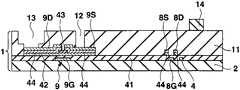
도 2∼도 7을 이용하여 발광소자인 유기일렉트로루미네선트소자를 화소로 하는 표시장치의 제조방법에 대하여 설명한다. 도 2∼도 7은 제조방법에 있어서의 각 공정의 단면도이고, 공정순서는 도 2∼도 7의 차례로 되어 있다.The manufacturing method of the display apparatus which uses the organic electroluminescent element which is a light emitting element as a pixel is demonstrated using FIG. 2-7 is sectional drawing of each process in a manufacturing method, and the process order is in order of FIG.

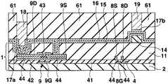
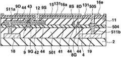
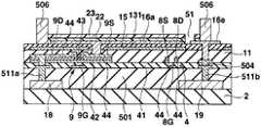
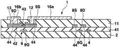
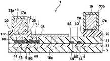
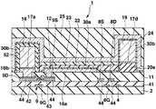
우선 도 1, 도 2에 나타내는 바와 같은 화소회로를 갖는 트랜지스터어레이기판(1)을 제조한다. 이 트랜지스터어레이기판(1)은 유기EL소자를 제어하는 화소회로(6)가 종래와 같이 신호전압에 의한 전압휘도계조제어하는 것은 아니고, 휘도계조데이터에 따른 전류값의 휘도계조전류(기억전류)를 화소회로(6) 내에 흘림으로써 휘도계조전류의 전류값에 따른 전류값의 구동전류를 가져오고, 이 구동전류를 후술하는 유기EL소자(26)에 흘림으로써 계조제어하는 전류휘도계조제어패널이며, 기상성장법(예를 들면, PVD법, CVD법, 스퍼터링법 등)과 같은 성막공정, 포토리소그래 피법, 메탈마스크법과 같은 마스크공정, 에칭과 같은 형상가공공정을 적절하게 실시함으로써 화소회로(6)의 일부가 되는 복수의 트랜지스터나 커패시터(10: capacitor)를 기판(2)상에 패터닝함으로써 제조된 것이다.First, atransistor array substrate 1 having a pixel circuit as shown in Figs. 1 and 2 is manufactured. In thistransistor array substrate 1, thepixel circuit 6 for controlling the organic EL element does not control voltage luminance gradation by signal voltage as in the prior art, but the luminance gradation current (memory current) of the current value according to the luminance gradation data. Is a current luminance gradation control panel for bringing the driving current of the current value according to the current value of the luminance gradation current by flowing into thepixel circuit 6, and gradation control by flowing the driving current to theorganic EL element 26 which will be described later. To form a pixel circuit (eg, a PVD method, a CVD method, a sputtering method, etc.), a photolithography method, a mask process such as a metal mask method, or a shape processing process such as etching. And a plurality of transistors (capacitors) 10 which are part of 6) are patterned on thesubstrate 2.

구체적으로는 도 1에 나타내는 바와 같이, 트랜지스터어레이기판(1)은 유리, 또는 수지 등을 시트상 또는 판상으로 형성한 절연성의 기판(2)과, 서로 평행하게 되도록 기판(2)상에 배열된 복수의 신호전류선(데이터라인)(3, 3, ···)과, 기판(2)의 평면에서 보아 신호전류선(3)에 대하여 직교하도록 또한 서로 평행하게 되도록 기판(2)상에 배열된 복수의 주사선(4, 4, ···)과, 주사선(4, 4, ···)의 각각의 사이에 있어서 주사선(4)과 평행하게 되도록 기판(2)상에 배열된 복수의 전류원라인(18, 18, ···) 및 EL라인(19, 19, ···)과, 신호전류선(3, 3, ···) 및 주사선(4, 4, ···)을 따라서 이차원어레이상이 되도록 기판(2)상에 배열된 복수의 화소회로(6, 6, ···) 등을 구비하고 있다.Specifically, as shown in FIG. 1, thetransistor array substrate 1 is arranged on thesubstrate 2 so as to be in parallel with the insulatingsubstrate 2 formed of sheet or plate of glass, resin, or the like. Arranged on thesubstrate 2 such that the plurality of signal current lines (data lines) 3, 3,..., And thesubstrate 2 are orthogonal to and parallel to the signalcurrent line 3 in a plan view of thesubstrate 2. A plurality of current sources arranged on thesubstrate 2 so as to be parallel to thescanning line 4 between each of the plurality ofscanning lines 4, 4,..., And thescanning lines 4, 4,... Two-dimensional alonglines 18, 18, ... andEL lines 19, 19, ..., signalcurrent lines 3, 3, ... andscanning lines 4, 4, ... A plurality ofpixel circuits 6, 6, ... and the like arranged on thesubstrate 2 so as to form an array are provided.

화소회로(6)는 화소마다 화소의 주변에 설치된 회로이다. 화소회로(6)는 세개의 박막트랜지스터(이하, 간단하게 트랜지스터로 기술(記述)한다)(7, 8, 9)와, 커패시터(10)를 갖고 있다. 어떠한 트랜지스터(7, 8, 9)도 게이트(7G, 8G, 9G)(도 2 등에 도시), 게이트(7G, 8G, 9G)를 피복한 게이트절연막(41)(도 2 등에 도시), 게이트절연막(41)을 끼워서 각 게이트(7G, 8G, 9G)에 대향한 반도체층(42)(도 2 등에 도시), 반도체층(42)의 채널표면을 에찬트(etchant)로부터 보호하는 블록킹절연막(43)(도 2 등에 도시), 반도체층(42)의 양단부상에 형성된 불순물반도체층(44, 44)(도 2 등에 도시), 한쪽의 불순물반도체층(44)상에 형성된 드레인(7D, 8D, 9D)( 도 2 등에 도시), 다른쪽의 불순물반도체층(44)상에 형성된 소스(7S, 8S, 9S)(도 2 등에 도시) 등을 구비하는 N채널MOS형의 전계효과트랜지스터이고, 특히 비정질실리콘을 반도체층(42)(채널영역)으로 한 a-Si트랜지스터인데, 폴리실리콘을 반도체층(42)으로 한 p-Si트랜지스터라도 좋다. 트랜지스터(7, 8, 9)의 구조는 역스태거형이라도 좋고, 코플레이너형, 그 외의 형이라도 좋다. 이하에서는 트랜지스터(7)를 전류경로제어트랜지스터(7)와, 트랜지스터(8)를 홀딩트랜지스터(8)와, 트랜지스터(9)를 전류제어트랜지스터(9)로 칭한다. 여기에서 전류경로제어트랜지스터(7) 및 홀딩트랜지스터(8)를 구비한 회로가 선택기간 중에는 신호전류선(3)에 소정의 전류값의 기억전류를 흘리는 동시에, 비선택기간 중에는 신호전류선(3)에 전류를 흘리는 것을 정지하는 스위치회로에 상당하고, 전류제어트랜지스터(9) 및 커패시터(10)를 구비한 회로가 선택기간 중에 신호전류선(3)을 통하여 흐르는 기억전류의 전류값에 따른 전류데이터를 기억하며, 그 선택기간 중에 기억된 전류데이터에 따라서 기억전류의 전류값에 따른 전류값의 구동전류를 비선택기간 중에 유기EL소자(26)(도 8에 도시)에 공급하는 전류기억회로에 상당한다. 또 전류경로제어트랜지스터(7)는 비선택기간 중에 전류제어트랜지스터(9)로부터 흐르는 구동전류를 신호전류선(3)에 흘리지 않고, 유기EL소자(26)에 흘리도록 전류경로를 제어하는 기능을 갖는다. 홀딩트랜지스터(8)는 선택기간에 흐르는 기억전류의 전류값에 따른 전류제어트랜지스터(9)의 게이트(9S)-소스(9S)의 전압을 비선택기간까지 홀딩하는 기능을 갖는다. 또한 도 2∼도 7은 전류제어트랜지스터(9)를 주사선(4)에 직교하는 면을 따라서 절단한 경우의 트랜지스터어레이기판(1)의 단면도이며, 하나의 화소를 나타 낸다. 다른 화소도 각 공정에서는 도 2∼도 7의 상태로 되어 있다.Thepixel circuit 6 is a circuit provided around the pixel for each pixel. Thepixel circuit 6 includes three thin film transistors (hereinafter, simply described as transistors) 7, 8, and 9, and acapacitor 10. Any of thetransistors 7, 8, and 9 hasgates 7G, 8G, and 9G (shown in Fig. 2, etc.), a gate insulating film 41 (shown in Fig. 2, etc.) covering thegates 7G, 8G, and 9G, and a gate insulating film. A blocking insulatingfilm 43 which protects the channel surface of the semiconductor layer 42 (shown in FIG. 2 and the like) and the channel surface of thesemiconductor layer 42 facing eachgate 7G, 8G, and 9G by sandwiching the 41. (Shown in FIG. 2 and the like), impurity semiconductor layers 44 and 44 (shown in FIG. 2 and the like) formed on both ends of thesemiconductor layer 42, and drains 7D and 8D formed on oneimpurity semiconductor layer 44. 9D) (shown in FIG. 2 and the like), N-channel MOS type field effecttransistors having sources 7S, 8S and 9S (shown in FIG. 2 and the like) formed on the otherimpurity semiconductor layer 44, and the like. An a-Si transistor having amorphous silicon as the semiconductor layer 42 (channel region) may be a p-Si transistor having polysilicon as thesemiconductor layer 42. The structures of thetransistors 7, 8, 9 may be inverse staggered types, coplanar type, or other types. Hereinafter, thetransistor 7 is referred to as a currentpath control transistor 7, thetransistor 8 as a holdingtransistor 8, and thetransistor 9 as acurrent control transistor 9. Here, the circuit including the currentpath control transistor 7 and the holdingtransistor 8 flows the storage current of a predetermined current value to the signalcurrent line 3 during the selection period, and at the same time, the signalcurrent line 3 during the non-selection period. (C) corresponds to a switch circuit for stopping the flow of current through the circuit, and a circuit comprising thecurrent control transistor 9 and thecapacitor 10 is in accordance with the current value of the storage current flowing through the signalcurrent line 3 during the selection period. Current storage circuit for storing data and supplying driving current of the current value according to the current value of the storage current to the organic EL element 26 (shown in FIG. 8) during the non-selection period in accordance with the current data stored during the selection period. Corresponds to The currentpath control transistor 7 has a function of controlling the current path so as to flow the drive current flowing from thecurrent control transistor 9 to the signalcurrent line 3 during the non-selection period, and not to the signalcurrent line 3. Have The holdingtransistor 8 has a function of holding the voltage of thegate 9S-source 9S of thecurrent control transistor 9 in accordance with the current value of the storage current flowing in the selection period until the non-selection period. 2 to 7 are cross-sectional views of thetransistor array substrate 1 in the case where thecurrent control transistor 9 is cut along the plane orthogonal to thescan line 4, and shows one pixel. Other pixels are also in the states of Figs.

도 1에 나타내는 바와 같이, 전류경로제어트랜지스터(7)의 게이트(7G)는 주사선(4)에 접속되고, 전류경로제어트랜지스터(7)의 소스(7S)는 신호전류(3)에 접속되며, 전류경로제어트랜지스터(7)의 드레인(7D)은 전류제어트랜지스터(9)의 소스(9S)에 접속되어 있다. 홀딩트랜지스터(8)의 게이트(8G)는 주사선(4)에 접속되고, 홀딩트랜지스터(8)의 드레인(8D)은 전류제어트랜지스터(9)의 드레인(9D) 및 전류원라인(18)에 접속되며, 홀딩트랜지스터(8)의 소스(8S)는 전류제어트랜지스터(9)의 게이트(9G)에 접속되어 있다. 전류제어트랜지스터(9)의 드레인(9D)은 전류원라인(18)에 접속되어 있다. 커패시터(10)는 전류제어트랜지스터(9)의 게이트(9G)에 접속된 전극과, 전류제어트랜지스터(9)의 소스(9S)에 접속된 전극과, 이들 두개의 전극의 사이에 개재하는 유전체막을 갖고, 전류제어트랜지스터(9)의 게이트(9G)와 소스(9S)의 사이에 전하를 축적하는 기능을 갖는다. 커패시터(10)의 유전체막은 게이트절연막(41)을 가져도 좋다.As shown in Fig. 1, thegate 7G of the currentpath control transistor 7 is connected to thescanning line 4, thesource 7S of the currentpath control transistor 7 is connected to the signal current 3, Thedrain 7D of the currentpath control transistor 7 is connected to thesource 9S of thecurrent control transistor 9. Thegate 8G of the holdingtransistor 8 is connected to thescan line 4, thedrain 8D of the holdingtransistor 8 is connected to thedrain 9D and thecurrent source line 18 of thecurrent control transistor 9. Thesource 8S of the holdingtransistor 8 is connected to thegate 9G of thecurrent control transistor 9. Thedrain 9D of thecurrent control transistor 9 is connected to thecurrent source line 18. Thecapacitor 10 includes an electrode connected to thegate 9G of thecurrent control transistor 9, an electrode connected to thesource 9S of thecurrent control transistor 9, and a dielectric film interposed between these two electrodes. And accumulates electric charges between thegate 9G and thesource 9S of thecurrent control transistor 9. The dielectric film of thecapacitor 10 may have agate insulating film 41.

상기 트랜지스터(7, 8, 9)는 동일 공정에서 동시에 패터닝된 것이기 때문에 게이트(7G, 8G, 9G), 게이트절연막(41), 반도체층(42), 불순물반도체층(44), 드레인(7D, 8D, 9D), 소스(7S, 8S, 9S) 등의 조성은 트랜지스터(7, 8, 9)의 사이에서 같지만, 트랜지스터(7, 8, 9)의 형상, 크기, 치수, 채널폭, 채널길이 등은 트랜지스터(7, 8, 9)의 각각의 기능에 따라서 다르다.Since thetransistors 7, 8, and 9 are simultaneously patterned in the same process, thegates 7G, 8G, and 9G, thegate insulating film 41, thesemiconductor layer 42, theimpurity semiconductor layer 44, and thedrain 7D, The composition of the 8D and 9D and thesources 7S, 8S, and 9S are the same among thetransistors 7, 8, and 9, but the shape, size, dimensions, channel width, and channel length of thetransistors 7, 8, and 9 are the same. Etc. differ depending on the respective functions of thetransistors 7, 8, 9;

신호전류선(3, 3,···)은 트랜지스터(7, 8, 9)의 각 소스(7S, 8S, 9S), 드레인(7D, 8D, 9D)이 되는 소스, 드레인도전막을 동일 공정에서 동시에 패터닝함으 로써 형성된 것이다.The signalcurrent lines 3, 3, ... are used for the source and drain conductive films which become therespective sources 7S, 8S, 9S and drains 7D, 8D, 9D of thetransistors 7, 8, 9 in the same process. It is formed by patterning at the same time.

주사선(4, 4, ···)은 트랜지스터(7, 8, 9)의 각 게이트(7G, 8G, 9G)가 되는 게이트도전막을 동일 공정에서 동시에 패터닝함으로써 형성된 것이다.Thescanning lines 4, 4, ... are formed by simultaneously patterning the gate conductive films serving as thegates 7G, 8G, 9G of thetransistors 7, 8, 9 in the same process.

또 도 9에 나타내는 배선(36, 36), 배선(39, 39), 복수의 배선(45)은 모두 하층이 게이트도전막을 패터닝하여 이루어지고, 상층이 소스, 드레인도전막을 패터닝하여 이루어지는 것이다. 배선(36, 36), 배선(39, 39), 복수의 배선(45)은 모두 비표시영역에 설치되어 있기 때문에 게이트도전막이나 소스, 드레인도전막과 같이 얇아도 폭넓게 설치함으로써 충분히 저저항으로 할 수 있다.In thewirings 36 and 36, thewirings 39 and 39, and the plurality ofwirings 45 shown in FIG. 9, the lower layer is formed by patterning the gate conductive film, and the upper layer is formed by patterning the source and drain conductive films. Since thewirings 36 and 36, thewirings 39 and 39, and the plurality ofwirings 45 are all provided in the non-display area, they are sufficiently widened even if they are thin like the gate conductive film, the source, or the drain conductive film. can do.

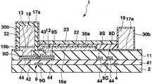
또 도 2에 나타내는 바와 같이, 트랜지스터어레이기판(1)의 표층에는 평탄화막(11)이 전체 일면에 성막되어 있고, 평탄화막(11)에 의해서 신호전류선(3, 3, ···), 주사선(4, 4, ···) 및 화소회로(6, 6, ···)가 피복되어 있다. 평탄화막(11)은 트랜지스터(7, 8, 9)를 보호하기 위한 질화실리콘, 산화실리콘 등의 무기층간 절연막상에 표면이 평탄화될 정도로 두껍게 성막되는 폴리이미드 등의 감광성 절연막을 적층한 것이다. 또한 트랜지스터어레이기판(1)의 각층 중, 기판(2)의 표면으로부터 평탄화막(11)의 표면까지의 사이의 다층막을 트랜지스터층이라 한다.As shown in Fig. 2, theplanarization film 11 is formed on the entire surface of thetransistor array substrate 1, and the signalcurrent lines 3, 3, ... are formed by theplanarization film 11; Thescanning lines 4, 4, ... and thepixel circuits 6, 6, ... are covered. Theplanarization film 11 is formed by stacking a photosensitive insulating film such as polyimide formed on the inorganic interlayer insulating film of silicon nitride, silicon oxide or the like for protecting thetransistors 7, 8, 9 to be thick enough to flatten the surface. In each layer of thetransistor array substrate 1, a multilayer film between the surface of thesubstrate 2 and the surface of theplanarization film 11 is called a transistor layer.

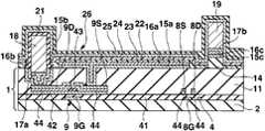
도 2에 나타내는 바와 같이, 준비한 트랜지스터어레이기판(1)에 대하여 포토리소그래피법, 에칭법 등을 실시함으로써 각 전류제어트랜지스터(9)의 소스(9S)에 통하는 컨택트홀(12) 및 각 전류제어트랜지스터(9)의 드레인(9D)에 통하는 컨택트홀(13)을 평탄화막(11)에 형성한다. 동시에 배선(36, 36)의 각 일단부상의 평탄화막(11)에 컨택트홀(37, 37)을 형성하고, 배선(39, 39)의 각 일단부상의 평탄화막 (11)에 컨택트홀(40, 40)을 형성하며, 각 전류원라인(18, 18, ···)의 단부에 컨택트홀(46)을 형성한다.As shown in Fig. 2, the preparedtransistor array substrate 1 is subjected to a photolithography method, an etching method, or the like, so that the contact holes 12 and the respective current control transistors that communicate with thesource 9S of eachcurrent control transistor 9 are provided. Acontact hole 13 through thedrain 9D of (9) is formed in theplanarization film 11. At the same time, contact holes 37 and 37 are formed in the flatteningfilm 11 on each end of thewirings 36 and 36, and contact holes 40 are formed in the flatteningfilm 11 on each one of thewirings 39 and 39. And 40, and contact holes 46 are formed at the ends of eachcurrent source line 18, 18,...

다음으로 질화실리콘 또는 산화실리콘으로 이루어지는 유기EL분리절연막(14)을 세로방향(열방향)에 이웃한 화소의 사이에 있어서 주사선(4)과 평행하게 되도록 패터닝 형성한다. 유기EL분리절연막(14)은 기상성장법과 같은 박막형성공정, 포토리소그래피법과 같은 마스크공정, 에칭법과 같은 형상가공공정을 거쳐서 패터닝한다.Next, the organic ELisolation insulating film 14 made of silicon nitride or silicon oxide is patterned so as to be parallel to thescanning line 4 between pixels adjacent in the vertical direction (column direction). The organic ELisolation insulating film 14 is patterned through a thin film forming process such as a vapor phase growth method, a mask process such as a photolithography method, and a shape processing process such as an etching method.

다음으로 도 3에 나타내는 바와 같이, 스퍼터링 등의 기상성장법에 의해서 금, 은, 동, 알루미늄, 티탄 또는 크롬 등의 금속재료로 이루어지는 고반사율의 반사금속막(15)을 트랜지스터어레이기판(1)상의 일면에 성막한다. 반사금속막(15)은 컨택트홀(12, 13) 내에 있어서도 표면에 성막된다.Next, as shown in FIG. 3, the highlyreflective metal film 15 made of metal materials, such as gold, silver, copper, aluminum, titanium, or chromium, is formed by the vapor phase growth method such as sputtering. We deposit on one side of the statue. Thereflective metal film 15 is also formed on the surface of the contact holes 12 and 13.

다음으로 스퍼터링 등의 기상성장법에 의해서 투명금속산화물막(16)을 반사금속막(15)상의 일면에 성막한다. 투명금속산화물막(16)은 산화인듐, 산화아연 혹은 산화주석 또는 이들 중의 적어도 하나를 포함하는 혼합물(예를 들면, 주석도프산화인듐(ITO), 아연도프산화인듐, 카드뮴-주석산화물(CTO))로 이루어진다. 투명금속산화물막(16)은 컨택트홀(12, 13) 내에 있어서도 표면에 성막된다.Next, the transparentmetal oxide film 16 is formed on one surface on thereflective metal film 15 by a vapor phase growth method such as sputtering. The transparentmetal oxide film 16 may be formed of indium oxide, zinc oxide or tin oxide, or a mixture containing at least one of these (eg, indium tin dope oxide (ITO), indium zinc dope oxide, cadmium tin oxide (CTO)). ) The transparentmetal oxide film 16 is also formed on the surface of the contact holes 12 and 13.

다음으로 스퍼터링 등의 기상성장법에 의해서 30nm∼50nm정도의 두께의 동 또는 니켈 등의 금속재료로 이루어지는 하층 및 이 하층상에 전해도금 등에 의해 500nm정도의 동 등의 상층을 갖는 금속층(17)을 투명금속산화물막(16)상의 일면에 성막한다.Subsequently, ametal layer 17 having a lower layer made of a metal material such as copper or nickel having a thickness of about 30 nm to 50 nm by a vapor phase growth method such as sputtering and an upper layer of copper or the like having about 500 nm by electroplating or the like on the lower layer is formed. The film is formed on one surface of the transparentmetal oxide film 16.

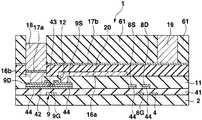
다음으로 컨택트홀(13)과 겹치고 또한 행방향을 따른 부분의 금속층(17) 및 유기EL분리절연막(14)과 겹치며 또한 행방향을 따른 부분의 금속층(17)이 노출되는 포토레지스트막(61)을 형성한다. 동시에 포토레지스트막(61)은 컨택트홀(37)에서 배선(36)과 접속된 금속층(17)을 노출하고, 컨택트홀(40)에서 배선(39)과 접속된 금속층(17)을 노출하며, 또한 각 컨택트홀(46)에서 배선(45)과 접속된 금속층(17)을 노출하고 있다.Next, thephotoresist film 61 overlapping thecontact hole 13 and overlapping themetal layer 17 and the organic ELisolation insulating film 14 in the portion along the row direction and exposing themetal layer 17 in the portion along the row direction is exposed. To form. At the same time, thephotoresist film 61 exposes themetal layer 17 connected to thewiring 36 in thecontact hole 37, and exposes themetal layer 17 connected to thewiring 39 in thecontact hole 40. In addition, themetal layer 17 connected to thewiring 45 is exposed in eachcontact hole 46.

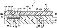
이어서 노출된 금속층(17)을 전극으로서 전해도금을 실시함으로써, 도 4에 나타내는 바와 같이 노출된 금속층(17)상에 각각 막두께 2㎛∼100㎛ 또한 2㎛∼50㎛폭의 동 등의 도금의 전류원라인(18, 18, ···), EL라인(19, 19, ···), 또한 EL라인(19, 19, ···)을 표시영역 외의 좌측에서 서로 접속하는 공통배선(35), 및 EL라인(19, 19, ···)을 표시영역 외의 우측에서 서로 접속하는 공통배선(38)을 형성한다. 공통배선(35)은 컨택트홀(37, 37)을 통하여 배선(36, 36)에 접속되고, 공통배선(38)은 컨택트홀(40, 40)을 통하여 배선(39, 39)에 접속되어 있다. 전류원라인(18, 18, ···)은 각 컨택트홀(46)을 통하여 각 배선(45, 45, ···)에 접속되어 있다.Subsequently, electroplating is performed using the exposedmetal layer 17 as an electrode, thereby plating on the exposedmetal layer 17, such as copper having a thickness of 2 µm to 100 µm and a width of 2 µm to 50 µm, respectively, as shown in FIG.Common wiring 35 connecting current source lines 18, 18, ..., EL lines 19, 19, ..., andEL lines 19, 19, ... ) And the EL lines 19, 19, ... are formed on the right side outside the display area. Thecommon wiring 35 is connected to thewirings 36 and 36 through the contact holes 37 and 37, and thecommon wiring 38 is connected to thewirings 39 and 39 through the contact holes 40 and 40. . The current source lines 18, 18, ... are connected to therespective wirings 45, 45, ... through the respective contact holes 46.

전류원라인(18, 18, ···), EL라인(19, 19, ···), 공통배선(35) 및 공통배선(38)은 모두 트랜지스터(7, 8, 9)의 소스(7S, 8S, 9S) 및 드레인(7D, 8D, 9D)의 막두께 보다도 두꺼워지도록 퇴적되고, 전류원라인(18, 18, ···), EL라인(19, 19, ···), 공통배선(35) 및 공통배선(38)의 각 단위길이당의 저항은 모두 트랜지스터(7, 8, 9)의 소스(7S, 8S, 9S) 및 드레인(7D, 8D, 9D)의 단위길이당의 저항보다도 작다. 또한 전류원라인(18, 18, ···), L라인(19, 19, ···), 공통배선(35) 및 공통배선(38)의 저항율(물질의 비저항)은 모두 트랜지스터(7, 8, 9)의 소스(7S, 8S, 9S) 및 드레인(7D, 8D, 9D)의 도전재료의 저항율(물질의 비저항) 보다도 낮은 것이 바람직하다. 또 전류원라인(18, 18, ···), L라인(19, 19, ···), 공통배선(35) 및 공통배선(38)은 모두 트랜지스터(7, 8, 9)의 게이트(7G, 8G, 9G)의 막두께보다도 두꺼워지도록 퇴적되고, 전류원라인(18, 18, ···), L라인(19, 19, ···), 공통배선(35) 및 공통배선(38)의 단위길이당의 저항은 모두 트랜지스터(7, 8, 9)의 게이트(7G, 8G, 9G)의 단위길이당의 저항보다도 작다. 전류원라인(18, 18, ···), L라인(19, 19, ···), 공통배선(35) 및 공통배선(38)의 저항율은 모두 트랜지스터(7, 8, 9)의 게이트(7G, 8G, 9G)의 도전재료의 저항율보다도 낮은 것이 바람직하다. 또한 전류원라인(18)이 화소회로접속배선의 도전층에 상당하고, 주사선(4)을 따라서 동일한 행에 배열된 화소회로(6, 6, ···)가 동일한 전류원라인(18)에 접속되어 있다. 이와 같이 전류원라인(18, 18, ···), EL라인(19, 19, ···), 공통배선(35) 및 공통배선(38)은 저항이고, 긴길이에 형성되어 있는 것에 대하여 배선(36, 36), 배선(39, 39) 및 각 배선(45)은 비교적 짧기 때문에 전체의 배선저항에의 영향이 작다.The current source lines 18, 18, ..., EL lines 19, 19, ..., thecommon wiring 35 and thecommon wiring 38 are all thesources 7S, 8S, 9S) and are deposited to be thicker than the film thicknesses of thedrains 7D, 8D, and 9D, and the current source lines 18, 18, ..., EL lines 19, 19, ...,common wiring 35 And the resistance per unit length of thecommon wiring 38 are all smaller than the resistances per unit length of thesources 7S, 8S, 9S and thedrains 7D, 8D, 9D of thetransistors 7, 8, 9. In addition, the resistivity (specific resistance of the material) of the current source lines 18 and 18, the L lines 19 and 19, and thecommon wiring 35 and thecommon wiring 38 are alltransistors 7 and 8. It is preferable that the resistivity (specific resistance of the material) of the conductive material of thesources 7S, 8S, 9S and 9 and thedrains 7D, 8D, and 9D of 9 be preferable. In addition, the current source lines 18, 18, ..., the L lines 19, 19, ..., thecommon wiring 35 and thecommon wiring 38 are allgates 7G of thetransistors 7, 8, 9; , 8G, 9G) to be thicker than the film thicknesses, and the current source lines 18, 18, ..., L lines 19, 19, ..., thecommon wiring 35 and thecommon wiring 38 The resistance per unit length is all smaller than the resistance per unit length of thegates 7G, 8G and 9G of thetransistors 7, 8 and 9. The resistivity of the current source lines 18, 18, ..., the L lines 19, 19, ..., thecommon wiring 35 and thecommon wiring 38 are all the gates of thetransistors 7, 8, 9 ( It is preferable that it is lower than the resistivity of the electrically-conductive material of 7G, 8G, 9G). Further, thecurrent source line 18 corresponds to the conductive layer of the pixel circuit connection wiring, and thepixel circuits 6, 6, ... arranged in the same row along thescanning line 4 are connected to the samecurrent source line 18, have. Thus, the current source lines 18, 18, ..., EL lines 19, 19, ..., thecommon wiring 35 and thecommon wiring 38 are resistors, and the wirings are formed in a long length. (36, 36), thewirings 39 and 39, and each of thewirings 45 are relatively short, so that the influence on the overall wiring resistance is small.

전류원라인(18, 18, ···)의 개수, EL라인(19, 19, ···)의 개수 및 배선(45, 45, ···)의 개수는 모두 주사선(4, 4, ···)의 개수와 동일수이고, 각행에 전류원라인(18), EL라인(19), 배선(45) 및 주사선(4)이 1개씩 설치되어 있다. 그 후, 포토레지스트막(61)을 제거한다. 또한 전해도금 대신에 스퍼터링법, 승화 증착법 또는 디스펜서법에 의해 동후막을 성막해도 좋다.The number of current source lines 18, 18, ..., the number ofEL lines 19, 19, ..., and the number ofwirings 45, 45, ... are all scanninglines 4, 4, ... ), And thecurrent source line 18, theEL line 19, thewiring 45 and thescanning line 4 are provided in each row one by one. Thereafter, thephotoresist film 61 is removed. Instead of electroplating, a copper thick film may be formed by sputtering, sublimation deposition, or dispenser.

그리고 전류원라인(18, 18, ···), EL라인(19, 19, ···), 공통배선(35) 및 공통배선(38)으로 피복된 부분을 제외하고 노출된 금속층(17)에 대하여 에칭에 의한 형상가공을 실시함으로써 전류원라인(18, 18, ···)의 아래쪽에 밑바탕층(17a)을 형성하고, EL라인(19, 19, ···)의 아래쪽에 밑바탕층(17b)을 형성한다.And the exposedmetal layer 17 except for portions covered with the current source lines 18, 18, ..., EL lines 19, 19, ...,common wiring 35 andcommon wiring 38. Forming by etching with respect to thebase layer 17a is formed under the current source lines 18, 18, ..., and underneath the EL lines 19, 19, ... ).

다음으로 도 5에 나타내는 바와 같이, 투명금속산화물막(16)에 대하여 포토리소그래피법, 에칭법을 실시함으로써 형성된 레지스트마스크를 마스크로 해서 투명금속산화물막(16)을 화소마다 잔류시켜서 화소전극(16a)을 패터닝 형성하는 동시에, 전류원라인(18, 18, ···)을 마스크로 한 밑바탕층(17a)의 아래쪽에 설치된 투명금속산화물막(16)을 잔류시켜서 투명금속산화물밑바탕막(16b)을 형성하고, 밑바탕층(17b)의 아래쪽에 설치된 투명금속산화물막(16)을 잔류시켜서 투명금속산화물밑바탕막(16c)을 형성한다. 여기에서 평면에서 보아 잔류한 화소전극(16a)이 컨택트홀(12)에 겹치고 또한 잔류한 화소전극(16a)이 화소마다 독립하도록 투명금속산화물막(16)이 패터닝되어 있다. 화소전극(16a)은 후술하는 유기EL소자(26)(도 8에 도시)의 애노드로서 기능한다. 밑바탕층(17a) 및 투명금속산화물밑바탕막(16b)은 전류원라인(18)과 형상이 대략 동일하고, 행방향으로 연장하고 있다. 밑바탕층(17b) 및 투명금속산화물밑바탕막(16c)은 EL라인(19)과 형상이 대략 동일하고, 행방향으로 연장하고 있다. 또한 도 5는 후술하는 도 8의 (Ⅴ)-(Ⅴ)선을 따른 면에 있어서 화살표방향으로 본 면의 단면도이다.Next, as shown in FIG. 5, the transparentmetal oxide film 16 is left for each pixel using the resist mask formed by performing the photolithography method and the etching method with respect to the transparentmetal oxide film 16, and pixel pixel 16a. ) And the transparentmetal oxide underlayer 16b formed under theunderlying layer 17a using the current source lines 18, 18, ... as a mask is left. The transparentmetal oxide film 16c is formed by leaving the transparentmetal oxide film 16 provided below thebase layer 17b. Here, the transparentmetal oxide film 16 is patterned such that the remainingpixel electrode 16a overlaps thecontact hole 12 in plan view and the remainingpixel electrode 16a is independent for each pixel. Thepixel electrode 16a functions as an anode of the organic EL element 26 (shown in FIG. 8) described later. Theunderlayer 17a and the transparentmetal oxide underlayer 16b have substantially the same shape as thecurrent source line 18 and extend in the row direction. Theunderlying layer 17b and the transparent metal oxideunderlying film 16c have substantially the same shape as theEL line 19 and extend in the row direction. FIG. 5 is a cross-sectional view of the plane viewed in the direction of the arrow in the plane along the lines (V)-(V) of FIG. 8 to be described later.

계속해서 화소전극(16a) 및 레지스트마스크를 마스크로 해서 반사금속막(15) 을 화소전극(16a)과 동일 형상으로 패터닝하여 반사금속밑바탕막(15a)을 형성하고, 투명금속산화물밑바탕막(16b)의 아래쪽의 반사금속막(15)을 잔류하도록 에칭하여 반사금속밑바탕막(15b)을 형성하며, 투명금속산화물밑바탕막(16c)의 아래쪽의 반사금속막(15)을 잔류하도록 에칭하여 반사금속밑바탕막(15c)을 형성한다. 또한 평면에서 보아 반사금속밑바탕막(15a)은 컨택트홀(12)에 겹치도록 배치되어 있다. 이 때문에 화소전극(16a)은 서로 화소마다 전기적으로 절연되고, 또한 해당 화소의 전류제어트랜지스터(9)의 소스(9S)와 접속되어 있다. 도 5의 상태의 트랜지스터어레이기판(1)의 회로도가 도 1이 된다.Subsequently, thereflective metal film 15 is patterned in the same shape as thepixel electrode 16a using thepixel electrode 16a and the resist mask as a mask to form a reflective metalunderlying film 15a, and the transparent metal oxide underlying film 16b. 2) to form thereflective metal underlayer 15b by etching the remainingreflective metal film 15 underneath the bottom surface, and to reflect thereflective metal film 15 under the transparentmetal oxide underlayer 16c. Theunderlayer film 15c is formed. In addition, the planarreflective base film 15a is disposed so as to overlap thecontact hole 12. For this reason, thepixel electrodes 16a are electrically insulated from each other for each pixel and are connected to thesource 9S of thecurrent control transistor 9 of the pixel. 1 is a circuit diagram of thetransistor array substrate 1 in the state shown in FIG.

그리고 이 유기EL소자(26)가 설치되어 있지 않은 구조의 트랜지스터어레이기판(1)에 있어서, 각 주사선(4)에 검사용 주사드라이버를 접속시키고, 전류원라인(18)에 소정의 전압을 출력하는 검사용 구동드라이버를 접속시키며, 신호전류선(3)에, 신호전류선(3)에 소정의 전류값의 전류가 흐르게 하는 검사용 전류제어드라이버를 접속시키고 나서 주사선(4), 전류원라인(18)에 구동드라이버로부터 소정의 전압을 인가하고, 전류제어드라이버로부터 신호전류선(3)에 소정의 전류가 흐르도록 구동시키며, 전류원라인(18)으로부터 각 화소회로(6)의 전류제어트랜지스터(9)의 소스(9S), 드레인(9D)간 및 전류경로제어트랜지스터(7)의 소스(7S), 드레인(7D)간을 경유하여 신호전류선(3)에 소정의 전류값의 전류가 흐르고 있는지 어떤지 검사할 수 있다. 이와 같이 유기EL소자(26)를 설치하는 전(前)단계로 각 화소회로(6)가 정상인지 아닌지 확인할 수 있기 때문에 가령 트랜지스터어레이기판(1)의 어떤 화소회로(6)의 트랜지스터(7, 8, 9), 커패시터(10)의 어느 쪽인가에 동작불량이 있 고, 불량품으로 확정된 경우, 그 트랜지스터어레이기판(1)에 유기EL소자(26)를 형성하지 않고 완료되기 때문에 생산성을 향상할 수 있다.In thetransistor array substrate 1 having the structure in which theorganic EL element 26 is not provided, an inspection scan driver is connected to eachscan line 4, and a predetermined voltage is output to thecurrent source line 18. The inspection drive driver is connected to the signalcurrent line 3, and the inspection current control driver for causing a current of a predetermined current value to flow through the signalcurrent line 3, and then thescan line 4 and thecurrent source line 18. A predetermined voltage is applied from the drive driver, and a predetermined current flows from the current control driver to the signalcurrent line 3, and thecurrent control transistor 9 of eachpixel circuit 6 is driven from thecurrent source line 18. Whether a current of a predetermined current value flows in the signalcurrent line 3 between thesource 9S and thedrain 9D of the Nr) and between thesource 7S and thedrain 7D of the currentpath control transistor 7. You can check how it looks. In this way, it is possible to confirm whether or not eachpixel circuit 6 is normal in the previous step of installing theorganic EL element 26. For example, thetransistors 7 of anypixel circuit 6 of thetransistor array substrate 1 can be checked. 8, 9) If either of thecapacitors 10 is defective in operation and is determined to be defective, the productivity is improved since theorganic EL element 26 is completed without forming theorganic EL element 26 on thetransistor array substrate 1. can do.

도 8은 도 5의 상태에 있어서의 화소회로(6)의 주요소의 대략 평면도이고, 전류원라인(18) 및 EL라인(19)은 주사선(4)에 대하여 평행하게 설치되어 있다. 또 도 5에 나타내는 바와 같이, 평면에서 보아 가로방향(행방향)으로 배열된 모든 화소, 즉 각 행의 화소의 컨택트홀(13)에 설치된 밑바탕층(17a)에 대하여 전류원라인(18)의 일부가 일치하도록 형성되어 있기 때문에 각 행의 모든 화소의 전류제어트랜지스터(9)의 드래인(9D)이 각 행의 전류원라인(18)에 각각 전기적으로 접속한 상태로 된다.FIG. 8 is a plan view of principal elements of thepixel circuit 6 in the state shown in FIG. 5, and thecurrent source line 18 and theEL line 19 are provided in parallel with thescan line 4. As shown in Fig. 5, part of thecurrent source line 18 with respect to all the pixels arranged in the horizontal direction (row direction) in plan view, that is, theunderlying layer 17a provided in the contact holes 13 of the pixels in each row. Are formed to coincide with each other, thedrain 9D of thecurrent control transistors 9 of all the pixels of each row is electrically connected to the current source lines 18 of each row.

또한 도 8에 있어서, 트랜지스터(7∼9)의 소스(7S, 8S, 9S)와 일체로 형성된 신호전류선(3)과, 트랜지스터(7∼9)의 게이트(7G 8G, 9G)와 일체로 형성된 주사선(4)의 사이에는 게이트절연막(41)에 더하여 반도체층(42)과 동일막을 패터닝하여 이루어지는 보호막(42a)이 형성되어 있다. 또 홀딩트랜지스터(8)의 소스(8S)와 전류제어트랜지스터(9)의 게이트(9G)는 게이트절연막(41)에 설치된 컨택트홀(31)을 통하여 서로 접속되어 있다.8, the signalcurrent line 3 formed integrally with thesources 7S, 8S, and 9S of the transistors 7-9, and thegates 7G 8G, 9G of the transistors 7-9 are integrally formed. Aprotective film 42a formed by patterning the same film as thesemiconductor layer 42 in addition to thegate insulating film 41 is formed between the formedscanning lines 4. Thesource 8S of the holdingtransistor 8 and thegate 9G of thecurrent control transistor 9 are connected to each other via acontact hole 31 provided in thegate insulating film 41.

다음으로 도 6에 나타내는 바와 같이, 각 전류원라인(18)에 전압을 인가한 전착도장법(electrodepositon coating)에 의해 전류원라인(18), 공통배선(35) 및 공통배선(38)의 표면만을 선택적으로 피복하도록 전류원라인절연막(21)을 형성한다. 또한 전류원라인절연막(21) 대신에 전류원라인(18), 공통배선(35) 및 공통배선(38)의 표면의 표면을 양극(陽極)산화하여 절연막을 피복시켜도 좋다.Next, as shown in FIG. 6, only the surfaces of thecurrent source line 18, thecommon wiring 35, and thecommon wiring 38 are selectively subjected to electrodeposition coating in which a voltage is applied to eachcurrent source line 18. The current sourceline insulating film 21 is formed so as to cover it. Instead of the current sourceline insulating film 21, the surfaces of thecurrent source line 18, thecommon wiring 35 and thecommon wiring 38 may be anodized to coat the insulating film.

또 기상성장법, 포토리소그래피법, 에칭법을 이용하여 전류원라인(18)만을 피복하도록 질화실리콘 또는 산화실리콘 등의 무기절연막 또는 발수성유기절연막으로 이루어지는 전류원라인절연막(21)을 패터닝해도 좋다. 또 마스크를 한 상태에서 스핀코트법을 실시하여 마스크를 벗김으로써(리프트오프법) 전류원라인(18)만을 피복하도록 절연재료로 이루어지는 전류원라인절연막(21)을 패터닝해도 좋다.Alternatively, the current sourceline insulating film 21 made of an inorganic insulating film such as silicon nitride or silicon oxide or a water-repellent organic insulating film may be patterned so as to cover only thecurrent source line 18 by using a vapor phase growth method, a photolithography method, or an etching method. Alternatively, the current sourceline insulating film 21 made of an insulating material may be patterned so as to cover only thecurrent source line 18 by performing a spin coating method in a masked state to remove the mask (lift-off method).

다음으로 도 6에 나타내는 바와 같이, PEDOT(폴리티오펜:polythiophene) 및 도펀트인 PSS(폴리스티렌술폰산)로 이루어지는 정공수송층(22)이 되는 용액을 액적토출법(잉크젯법), 스핀코트법, 딥코트법, 니들에 의한 적하법 등의 습식성막법에 의해서 성막한다. 정공수송층(22)은 트랜지스터어레이기판(1)의 일면에 형성하여 모든 화소에 공통시켜도 좋고, 화소마다 독립하도록 형성해도 좋다. 이 때 전류원라인절연막(21) 및 유기EL분리절연막(14)은 정공수송층재료함유용액이나 발광층재료함유용액에 대하여 발액성을 나타내는 것이 바람직하다. 발액성을 나타내면 정공수송층재료함유용액이나 발광층재료함유용액이 전류원라인(18), EL라인(19)을 따라서 치우쳐서 성막되지 않기 때문에 화소전극(16a)상에 균등한 두께로 성막할 수 있다. 도면에서는 정공수송층(22)을 포함하는 용액 또는 현탁액이 전류원라인(18) 및 EL라인(19)에 둘러싸여진 영역에 충전된 후, 용제 또는 수분이 휘발함으로써 정공수송층(22)이 성막되어 있는 상태를 나타내고 있다.Next, as shown in FIG. 6, the solution used as the hole-transport layer 22 which consists of PEDOT (polythiophene) and PSS (polystyrene sulfonic acid) which is a dopant is carried out by the droplet ejection method (inkjet method), spin coating method, and dip coat method. The film is formed by a wet film formation method such as a method and a dropping method using a needle. Thehole transport layer 22 may be formed on one surface of thetransistor array substrate 1 to be common to all the pixels, or may be formed so as to be independent for each pixel. At this time, the current sourceline insulating film 21 and the organic ELisolation insulating film 14 preferably exhibit liquid repellency with respect to the hole transporting layer material-containing solution or the light emitting layer material-containing solution. When liquid repellency is exhibited, the hole transporting layer material-containing solution or the light emitting layer material-containing solution is not deposited along thecurrent source line 18 and theEL line 19, so that the film can be formed with an even thickness on thepixel electrode 16a. In the figure, the solution or suspension including thehole transport layer 22 is filled in the region surrounded by thecurrent source line 18 and theEL line 19, and then the solvent or water is volatilized to form thehole transport layer 22. Indicates.

정공수송층(22)의 건조 후, 공역이중결합을 갖는 폴리파라비닐렌(polyparavinylene)계 발광재료나 폴리풀루오렌(polyfluorene)계 발광재료를 갖는 발광층(23)을 함유한 용액을 액적토출법(잉크젯법), 스핀코트법, 딥코트법, 니들에 의한 주입 등의 습식성막법에 의해서 성막한다. 발광층(23)은 도 9에 나타내는 바와 같이, 전류원라인(18) 및 EL라인(19)을 따라서 복수의 화소에 연속하여 형성되고, 각 행마다 적색으로 발광하는 적발광층(23R), 녹색으로 발광하는 녹발광층(23G), 청색으로 발광하는 청발광층(23B)이 된다. 여기에서 유기EL분리절연막(14)의 위에 반사금속밑바탕막(15c), 투명금속산화물밑바탕막(16c), 밑바탕층(17b) 및 EL라인(19)이 잔류하고 있는데, 정공수송층(22)의 막두께나 발광층(23)의 막두께는 유기EL분리절연막(14)의 막두께보다도 얇다. 그리고 정공수송층(22)이 되는 용액 또는 현탁액의 높이 및 화소영역에 피복했을 때의 발광층(23)이 되는 용액 또는 현탁액의 높이는 모두 전류원라인(18)의 높이나 EL라인(19)의 높이보다도 낮다. 따라서 정공수송층(22)이 되는 용액 또는 현탁액 및 발광층(23)이 되는 용액 또는 현탁액은 전류원라인(18) 및 EL라인(19)을 넘어서 이웃한 행의 화소에 유출하는 일은 없다. 이와 같이 전류원라인(18) 및 EL라인(19)은 정공수송층(22)이 되는 용액 또는 현탁액 및 발광층(23)이 되는 용액 또는 현탁액의 유출을 방지하는 격벽으로서 기능한다. 따라서 도 9에 나타내는 바와 같이, 전류원라인(18) 및 EL라인(19)을 따라서 둘러싸여진 행방향의 복수의 화소는 동일색으로 발광하는 발광층으로 하면 전류원라인(18) 및 EL라인(19)간에 일괄하여 발광층(23)을 포함하는 용액 또는 현탁액을 유입시킴으로써 행방향의 복수의 화소에 발광층(23)을 일괄하여 성막할 수 있다.After drying of thehole transport layer 22, a solution containing alight emitting layer 23 having a polyparavinylene-based light emitting material having a conjugated double bond or a polyfluorene-based light emitting material is droplet ejected (inkjet Film) by a wet film forming method such as spin coating, dip coating, needle injection, or the like. As shown in Fig. 9, thelight emitting layer 23 is formed in succession to a plurality of pixels along thecurrent source line 18 and theEL line 19, and emits light in red and redlight emitting layers 23R which emit red light in each row. The green luminescent layer 23G and the blueluminescent layer 23B emitting blue light. Here, thereflective metal underlayer 15c, the transparentmetal oxide underlayer 16c, theunderlayer 17b, and theEL line 19 remain on the organic ELisolation insulating film 14, and thehole transport layer 22 The film thickness and the film thickness of thelight emitting layer 23 are thinner than the film thickness of the organic ELisolation insulating film 14. The height of the solution or suspension to be thehole transport layer 22 and the height of the solution or suspension to be thelight emitting layer 23 when the pixel region is coated are lower than the height of thecurrent source line 18 and the height of theEL line 19. Therefore, the solution or suspension serving as thehole transport layer 22 and the solution or suspension serving as thelight emitting layer 23 do not flow over thecurrent source line 18 and theEL line 19 to the pixels in the adjacent rows. In this way, thecurrent source line 18 and theEL line 19 function as partition walls for preventing the outflow of the solution or suspension serving as thehole transport layer 22 and the solution or suspension serving as thelight emitting layer 23. Therefore, as shown in FIG. 9, when the plurality of pixels in the row direction surrounded by thecurrent source line 18 and theEL line 19 are light emitting layers emitting light of the same color, between thecurrent source line 18 and theEL line 19. By injecting the solution or suspension containing thelight emitting layer 23 collectively, thelight emitting layer 23 can be collectively formed into a some pixel of a row direction.

다음으로 도 7에 나타내는 바와 같이, 증착 등의 기상성장법에 의해서 마그네슘, 칼슘, 리튬, 바륨, 희토류금속 등의 낮은 일함수재료로 이루어지는 전자주입 층과, 산화인듐, 산화아연 또는 산화주석 또는 이들 중의 적어도 하나를 포함하는 혼합물(예를 들면, 주석도프산화인듐(ITO), 아연도프산화인듐, 카드뮴-주석산화물(CTO))을 갖는 투명도전층과의 이층구조의 공통전극(24)을 캐소드전극으로서 일면에 성막한다. 전자주입층은 10nm∼200nm의 두께로 가시광이 투과할 정도로 얇기 때문에 전류원라인(18)이나 EL라인(19)의 단차에 의해서 절단되어도 좋지만, 공통전극(24) 중의 투명도전층은 복수의 화소의 유기EL소자(26)의 한쪽의 전극을 서로 등전위로 하기 위해 전류원라인(18)상의 전류원라인절연막(21)의 위를 넘고 또한 EL라인(19)상에 걸치도록 성막되어 있다. 이에 따라 발광층(23)은 공통전극(24)에 밀착한 상태에서 공통전극(24)에 의해서 피복되고, 또한 EL라인(19)도 공통전극(24)에 밀착한 상태에서 공통전극(24)에 의해서 피복되어 공통전극(24)과 전기적으로 접속된다. 도 7에 있어서 화소전극(16a), 정공수송층(22), 발광층(23), 공통전극(24)의 차례로 적층한 것이 유기EL소자(26)가 되고, 공통전극(24)은 모든 화소(유기EL소자(26))를 덮도록 연속하여 형성되어 있다.Next, as shown in FIG. 7, the electron injection layer which consists of low work function materials, such as magnesium, calcium, lithium, barium, and rare earth metals by vapor phase growth methods, such as vapor deposition, indium oxide, zinc oxide, or tin oxide, or these The cathode electrode is formed of acommon electrode 24 having a two-layer structure with a transparent conductive layer having a mixture containing at least one of (e.g., indium tin dope oxide (ITO), indium zinc dope oxide, and cadmium-tin oxide (CTO)). As a film is formed on one side. Since the electron injection layer is thin enough to transmit visible light at a thickness of 10 nm to 200 nm, it may be cut by the step of thecurrent source line 18 or theEL line 19, but the transparent conductive layer in thecommon electrode 24 is formed of organic materials of a plurality of pixels. One electrode of theEL element 26 is formed over the current sourceline insulating film 21 on thecurrent source line 18 and over theEL line 19 so as to equipotentially. Accordingly, thelight emitting layer 23 is covered by thecommon electrode 24 in a state of being in close contact with thecommon electrode 24, and theEL line 19 is also in contact with thecommon electrode 24 in the state of being in close contact with thecommon electrode 24. Covered and electrically connected to thecommon electrode 24. In Fig. 7, theorganic EL element 26 is formed by laminating thepixel electrode 16a, thehole transport layer 22, thelight emitting layer 23, and thecommon electrode 24 in sequence, and thecommon electrode 24 includes all the pixels (organic). TheEL element 26 is formed continuously.

다음으로 스핀코트법, 딥코트법, 기상성장법에 의해서 오버코트절연층(25)을 일면에 성막한다.Next, theovercoat insulating layer 25 is formed on one surface by a spin coating method, a dip coating method and a vapor phase growth method.

그리고 도 9에 나타내는 바와 같이, 주사드라이버(32)의 각 단자를 각 배선(36)의 노출한 컨택트홀(37)과 반대측의 단부에 접속시킨다. 그리고 전류제어용의 데이터드라이버(33)의 각 단자를 각 신호전류선(3)의 노출한 단부에 접속시킨다. 또한 전류원드라이버(34)의 각 단자를 각 배선(45)을 통하여 각 전류원라인(18)에 접속한다. 또 주사드라이버(32) 및 전류원드라이버(34)로부터 출력되는 정전압 (VSS)이 배선(36), 배선(39), 공통배선(35), 공통배선(38) 및 EL라인(19)을 통하여 공통전극(24)에 공급되게 된다. 또한 기판(2)은 상면을 투명밀봉기판으로 덮어 유기EL소자(26)를 기판(2) 및 투명밀봉기판으로 밀봉해도 좋다. 이와 같이 하여 액티브매트릭스 구동방식의 표시장치가 완성된다.As shown in FIG. 9, each terminal of thescanning driver 32 is connected to the edge part on the opposite side to the exposedcontact hole 37 of eachwiring 36. As shown in FIG. Each terminal of thedata driver 33 for current control is connected to the exposed end of each signalcurrent line 3. In addition, each terminal of thecurrent source driver 34 is connected to eachcurrent source line 18 through eachwiring 45. The constant voltage VSS output from thescan driver 32 and thecurrent source driver 34 is common through thewiring 36, thewiring 39, thecommon wiring 35, thecommon wiring 38, and theEL line 19. It is supplied to theelectrode 24. In addition, thesubstrate 2 may be covered with a transparent sealing substrate and theorganic EL element 26 may be sealed with thesubstrate 2 and the transparent sealing substrate. In this way, an active matrix driving display device is completed.

완성된 표시장치는 도 10과 같은 회로를 구비한다. 도 10에 나타내는 바와 같이, 전류원라인(18)과 EL라인(19)의 사이에 있어서 전류제어트랜지스터(9)와 유기EL소자(26)가 직렬로 접속되어 있다. 즉, 전류제어트랜지스터(9)의 드레인(9D)이 전류원라인(18)에 접속되고, 전류제어트랜지스터(9)의 소스(9S)가 유기EL소자(26)의 애노드인 화소전극(16a)에 접속되며, 유기EL소자(26)의 캐소드인 공통전극(24)이 EL라인(19)에 접속되어 있다. 또 EL라인(19)이 발광소자접속배선의 도전층에 상당하고, 주사선(4)을 따라서 동일한 행에 배열된 유기EL소자(26, 26, ···)가 동일한 EL라인(19)에 접속되어 있다.The completed display device has a circuit as shown in FIG. As shown in FIG. 10, thecurrent control transistor 9 and theorganic EL element 26 are connected in series between thecurrent source line 18 and theEL line 19. As shown in FIG. That is, thedrain 9D of thecurrent control transistor 9 is connected to thecurrent source line 18, and thesource 9S of thecurrent control transistor 9 is connected to thepixel electrode 16a which is the anode of theorganic EL element 26. Thecommon electrode 24, which is a cathode of theorganic EL element 26, is connected to theEL line 19. TheEL line 19 corresponds to the conductive layer of the light emitting element connection wiring, and theorganic EL elements 26, 26, ... arranged in the same row along thescan line 4 are connected to thesame EL line 19. It is.

이 일렉트로루미네선트 디스플레이패널의 구동방법의 한 예를 설명한다.An example of the driving method of this electroluminescent display panel is demonstrated.

주사드라이버(32)가 복수의 주사선(4)에 ON레벨(하이레벨)의 시프트펄스를 차례차례 출력하고, 그것에 동기하도록 전류원드라이버(34)가 복수의 전류원라인(18)에 로우레벨(EL라인(19)의 정전압(VSS)보다도 저전위 또는 등전위)의 시프트펄스를 차례차례 출력하며, 각각 주사선(4)에 시프트펄스가 출력되어 있을 때에 데이터드라이버(33)가 신호전류선(3) 및 전류제어트랜지스터(9)에 접속된 전류경로제어트랜지스터(7)의 드레인(7D)-소스(7S)간을 통하여 강제적으로 전류제어트랜지스터(9)의 드레인(9D)-소스(9S)간에 휘도계조에 따른 전류값의 기억전류(뽑아냄전류)를 흘린다.Thescan driver 32 sequentially outputs an ON level (high level) shift pulse to the plurality ofscan lines 4, and thecurrent source driver 34 supplies a low level (EL line) to the plurality of current source lines 18 so as to synchronize with thescan driver 32. The shift pulses having a lower potential or an equipotential than the constant voltage VSS of (19) are sequentially output, and when the shift pulses are output to thescan lines 4, thedata driver 33 outputs the signalcurrent line 3 and the current. The luminance gradation between thedrain 9D and thesource 9S of thecurrent control transistor 9 is forced through thedrain 7D and thesource 7S of the currentpath control transistor 7 connected to thecontrol transistor 9. The storage current (extraction current) of the current value according to the flow.

구체적으로 어떤 행의 선택기간에 해당 행의 주사선(4)에 하이레벨의 시프트펄스가 출력되고, 또한 해당 행 이외의 복수의 주사선(4)에 OFF레벨(로우레벨)의 전압이 인가되어 있을 때는 해당 행의 전류원라인(18)에 EL라인(19)의 정전압(VSS)보다도 저전위 또는 등전위인 로우레벨의 시프트펄스가 출력되어 있다. 그 때 전류경로제어트랜지스터(7) 및 홀딩트랜지스터(8)가 ON상태(선택상태)가 된다. 이 때 데이터드라이버(33)가 계조데이터에 따른 전류값의 기억전류를 전류제어트랜지스터(9)의 드레인(9D)-소스(9S)간에 강제적으로 흐르도록 제어한다. 기억전류는 전류원라인(18)로부터 전류제어트랜지스터(9)의 드레인(9D)-소스(9S)간, 전류경로제어트랜지스터(7)의 드레인(7D)-소스(7S)간을 경유하여 신호전류선(3)을 향하여 흐른다. 이 기억전류의 전류값은 유기EL소자(26)의 발광휘도계조에 따라서 데이터드라이버(33)에 의해서 자동적으로 제어되어 있다.Specifically, when a high level shift pulse is output to thescanning line 4 of the row during a selection period of a row, and a voltage of the OFF level (low level) is applied to a plurality ofscanning lines 4 other than the row. A low-level shift pulse having a lower potential or an equipotential than the constant voltage VSS of theEL line 19 is output to thecurrent source line 18 of the row. At that time, the currentpath control transistor 7 and the holdingtransistor 8 are turned on (selection state). At this time, thedata driver 33 controls the storage current of the current value according to the gray scale data to be forced between thedrain 9D and thesource 9S of thecurrent control transistor 9. The storage current is signal current from thecurrent source line 18 between thedrain 9D and thesource 9S of thecurrent control transistor 9 and between thedrain 7D and thesource 7S of the currentpath control transistor 7. It flows towardline 3. The current value of this storage current is automatically controlled by thedata driver 33 in accordance with the light emission luminance gradation of theorganic EL element 26.

트랜지스터의 특성상 전류제어트랜지스터(9)의 드레인(9D)-소스(9S)간에 흐르는 전류의 전류값은 전류제어트랜지스터(9)의 게이트(9G)-소스(9S)간 전위 및 전류제어트랜지스터(9)의 드레인(9D)-소스(9S)간 전위에 의존된다. 데이터드라이버(33)는 기억전류의 전류값에 따라서 전류제어트랜지스터(9)의 게이트(9G)-소스(9S)간 전위 및 전류제어트랜지스터(9)의 드레인(9D)-소스(9S)간 전위를 설정하게 되고, 이 때의 게이트(9G)-소스(9S)간의 전압값은 전류제어트랜지스터(9)의 게이트(9G)-소스(9S)간의 커패시터(10)에 챠지된 전하에 의해서 그 후의 발광기간에 걸쳐서 홀딩(기억)된다. 해당 행의 선택기간 후의 발광기간에서는 주사드라이버(32)에 의해서 해당 행의 주사선(4)이 OFF레벨이 되고, 전류경로제어트랜지스터(7) 및 홀딩트랜지스터(8)이 OFF상태가 되는데, OFF상태의 홀딩트랜지스터(8)에 의해서 커패시터(10)의 전하가 홀딩되고, 전류제어트랜지스터(9)의 게이트(9G)-소스(9S)간의 전압이 그대로 유지된다. 이 때 전류원라인(18)이 하이레벨(EL라인(19)의 전압보다도 고레벨)이 됨으로써 전류제어트랜지스터(9)의 드레인(9D)-소스(9S)간이 포화상태가 될만큼 충분히 큰 전위치가 되기 때문에 전류원라인(18)으로부터 전류제어트랜지스터(9)를 통하여 유기EL소자(26)에 전류제어트랜지스터(9)의 게이트(9G)-소스(9S)간의 전압의 크기에 의해서 일의적으로 전류값이 정해지는 구동전류가 흐르고, 구동전류의 전류값에 따라서 유기EL소자(26)가 발광한다. 구동전류의 크기는 전류제어트랜지스터(9)의 게이트(9G)-소스(9S)간의 전압에 의존한다. 그 때문에 발광기간에 있어서의 구동전류의 전류값은 선택기간에 있어서의 기억전류의 전류값에 의해서 일의적으로 결정된다. 그리고 선택기간, 발광기간을 행마다 옮겨가는 것으로 일렉트로루미네선트 디스플레이패널이 프레임표시하는 것이 가능해진다.Due to the characteristics of the transistor, the current value of the current flowing between thedrain 9D and thesource 9S of thecurrent control transistor 9 is equal to the potential between thegate 9G and thesource 9S of thecurrent control transistor 9 and thecurrent control transistor 9. Depends on the potential between thedrain 9D and thesource 9S. Thedata driver 33 has a potential between thegate 9G and thesource 9S of thecurrent control transistor 9 and the potential between thedrain 9D and thesource 9S of thecurrent control transistor 9 according to the current value of the storage current. At this time, the voltage value between thegate 9G and thesource 9S is set by the charge charged in thecapacitor 10 between thegate 9G and thesource 9S of thecurrent control transistor 9 thereafter. It is held (memorized) over the light emission period. In the light emitting period after the selection period of the row, thescanning line 32 of the row is turned off by thescanning driver 32, and the currentpath control transistor 7 and the holdingtransistor 8 are turned off. The charge of thecapacitor 10 is held by the holdingtransistor 8, and the voltage between thegate 9G and thesource 9S of thecurrent control transistor 9 is maintained as it is. At this time, thecurrent source line 18 is at a high level (higher than the voltage of the EL line 19) so that the entire position is large enough so that thedrain 9D and thesource 9S of thecurrent control transistor 9 become saturated. Therefore, the current value is uniquely determined by the magnitude of the voltage between thegate 9G and thesource 9S of thecurrent control transistor 9 from thecurrent source line 18 to theorganic EL element 26 through thecurrent control transistor 9. The predetermined driving current flows, and theorganic EL element 26 emits light in accordance with the current value of the driving current. The magnitude of the drive current depends on the voltage between thegate 9G and thesource 9S of thecurrent control transistor 9. Therefore, the current value of the drive current in the light emitting period is uniquely determined by the current value of the storage current in the selection period. The electroluminescent display panel can display the frame by shifting the selection period and the light emission period from row to row.

상기한 바와 같이 신호전류선(3)으로 뽑아내어지는 기억전류의 전류값은 하나의 유기EL소자(26)에 흐르는 구동전류의 전류값에 거의 동등하기 때문에 신호전류선(3)은 트랜지스터(7, 8, 9)의 소스, 드레인과 같은 막을 이용해도 충분히 기능할 정도의 저항으로 설정할 수 있다. 또 주사선(4)은 전류경로제어트랜지스터(7) 및 홀딩트랜지스터(8)를 전압변조에 의해서 ON OFF제어하는 것만으로 좋으므로 반드시 대전류를 흘릴 필요가 없기 때문에, 트랜지스터(7, 8, 9)의 게이트와 같은 막을 이용해도 충분히 기능할 정도의 저항으로 설정할 수 있다.As described above, since the current value of the storage current extracted by the signalcurrent line 3 is almost equal to the current value of the driving current flowing through oneorganic EL element 26, the signalcurrent line 3 is atransistor 7 Can be set to a resistance enough to function. In addition, since thescan line 4 only needs to turn ON and OFF the currentpath control transistor 7 and the holdingtransistor 8 by voltage modulation, it is not necessary to flow a large current, so that thetransistors 7, 8, and 9 The same film as the gate can be used to set the resistor to be sufficiently functional.

그러나 어떤 행의 전류원라인(18)은 해당 행의 발광기간에 해당 행의 복수의 화소의 유기EL소자(26)에 각각 흐르는 구동전류의 전류원이 되기 때문에 큰 전류값의 전류가 흐르도록 저저항이 아니면 안된다. 그리고 어떤 행의 EL라인(19)에는 해당 행의 발광기간에 해당 행의 복수의 화소의 유기EL소자(26)에 각각 흐르는 구동전류가 합쳐져서 흐르기 때문에 큰 전류값의 전류가 흐르도록 저저항이 아니면 안된다. 이와 같은 전류원라인(18) 및 EL라인(19)의 저항은 각 행의 화소수(유기EL소자(26)의 수)가 많아짐에 따라 작게 하지 않으면 안되고, 화소수가 충분히 크면 트랜지스터(7, 8, 9)의 게이트와 같은 막을 이용한 것만으로는 충분히 전류를 흘릴 수 없게 되어버릴 우려가 있다.However, since thecurrent source line 18 of a row becomes a current source of driving current flowing through theorganic EL elements 26 of the plurality of pixels of the row during the light emission period of the row, low resistance is generated so that a current having a large current value flows. You must. In theEL line 19 of a row, the driving currents flowing through theorganic EL elements 26 of the plurality of pixels of the row are combined in the light emission period of the row, so that if the current having a large current value flows, Can not be done. The resistance of thecurrent source line 18 and theEL line 19 must be made smaller as the number of pixels (number of organic EL elements 26) in each row increases. If the number of pixels is large enough, thetransistors 7, 8, Using only the same film as the gate of 9) may not allow sufficient current to flow.

여기에서 본 실시형태에서는 전류원라인(18) 및 EL라인(19)을 트랜지스터(7, 8, 9)의 일부를 구성하는 도전막과는 다른 도전막으로 형성되어 있기 때문에 전류원라인(18, 18, ···) 및 EL라인(19, 19, ···)은 트랜지스터(7, 8, 9)의 소스(7S, 8S, 9S), 드레인(7D, 8D, 9D)의 막두께보다도 두껍게 퇴적할 수 있고, 소스(7S, 8S, 9S), 드레인(7D, 8D, 9D)에 대하여 단위길이당의 저항이 작게 설정되는 것이 가능해진다. 또 전류원라인(18, 18, ···) 및 EL라인(19 19, ···)은 트랜지스터(7, 8, 9)의 게이트(7G, 8G, 9G)의 막두께 보다도 두껍게 퇴적할 수 있고, 게이트(7G, 8G, 9G)에 대하여 단위길이당의 저항이 작게 설정되는 것이 가능해진다. 그 때문에 전류원라인(18)이나 EL라인(19)의 전기저항을 낮게 할 수 있고, 발광기간의 개시시로부터 유기EL소자(26)가 소망의 밝기(계조)로 발광하기까지의 시간의 지연을 억제하거나, 전류원라인(18)이나 EL라인(19)에 있어서의 전압강하를 억제하거나 할 수 있다. 또한 전류원라인(18)이나 EL라인(19)을 저저항으로 함으로써 일렉트로루미네선트 디스플레이패널의 밝기의 저하, 밝기의 불균형, 크로스토크 등의 표시악화를 억제할 수 있다.In this embodiment, since thecurrent source line 18 and theEL line 19 are formed of a conductive film different from the conductive film constituting a part of thetransistors 7, 8, 9, the current source lines 18, 18, ... andEL lines 19, 19, ... are thicker than the film thicknesses of thesources 7S, 8S, 9S and drains 7D, 8D, 9D of thetransistors 7, 8, 9; The resistance per unit length can be set small for thesources 7S, 8S, 9S and drains 7D, 8D, and 9D. Also, the current source lines 18, 18, andEL lines 19 19, ... can be thicker than the film thicknesses of thegates 7G, 8G, 9G of thetransistors 7, 8, 9, The resistance per unit length can be set small with respect to thegates 7G, 8G, and 9G. Therefore, the electrical resistance of thecurrent source line 18 and theEL line 19 can be lowered, and the delay of the time from the start of the light emission period until theorganic EL element 26 emits light at a desired brightness (gradation) can be reduced. The voltage drop in thecurrent source line 18 or theEL line 19 can be suppressed. In addition, by making thecurrent source line 18 and the EL line 19 a low resistance, it is possible to suppress display deterioration such as lowering of brightness, unbalance of brightness, crosstalk, etc. of the electroluminescent display panel.

예를 들면 전류원라인(18) 및 EL라인(19)을 배선폭 20㎛, 배선길이 664mm로 설정하여 또한 본 발명과 같이 막두께 5㎛의 동을 이용한 경우, 시트저항 0.003Ω/□, 저항 111Ω이 되고, 40mA로 했을 때의 전압강하는 4.4V로 억제된다. 한편 종래와 같이 트랜지스터(7, 8, 9)의 드레인, 소스에 이용한 막두께 0.3㎛의 Al-Ti를 전류원라인(18) 및 EL라인(19)로서 이용한 경우, 시트저항 0.5Ω/□, 저항 16600Ω이 되며, 40mA로 했을 때의 전압강하는 6644V로 되어 버린다.For example, when thecurrent source line 18 and theEL line 19 are set to a wiring width of 20 µm and a wiring length of 664 mm, and copper having a film thickness of 5 µm is used as in the present invention, the sheet resistance is 0.003 kΩ / square and the resistance 111 kΩ. The voltage drop at 40 mA is suppressed to 4.4 V. On the other hand, when Al-Ti having a film thickness of 0.3 µm used for the drains and sources of thetransistors 7, 8, and 9 is conventionally used as thecurrent source line 18 and theEL line 19, a sheet resistance of 0.5 k? /? It becomes 16600 kV, and the voltage drop when set to 40 mA becomes 6644 V.

또한 본 발명은 상기 실시형태에 한정되는 것은 아니고, 본 발명의 취지를 면탈하지 않는 범위에 있어서, 여러가지의 개량 및 설계의 변경을 실시해도 좋다.In addition, this invention is not limited to the said embodiment, You may change various improvement and a design in the range which does not deviate from the meaning of this invention.

예를 들면, 신호전류선(3)과 교차하는 부분을 제외한 주사선(4)이 노출하도록 게이트절연막(41) 및 평탄화막(11)에 컨택트홀을 설치하여 전류원라인(18)이나 EL라인(19)의 성막과 동일 공정에 있어서, 주사선(4)상에 도금층을 형성하여 주사선(4)을 저저항화해도 좋다. 이 도금층은 공통전극(24)과 절연하도록 전류원라인(18)의 전류원라인절연막(21)과 마찬가지로 공통전극(24)의 사이에 절연막을 개재시키고, 또 트랜지스터(7, 8)의 게이트와 전기적을 접속하고 있다.For example, contact holes are provided in thegate insulating film 41 and theplanarization film 11 to expose thescanning line 4 except for the portion intersecting the signalcurrent line 3, so that thecurrent source line 18 or theEL line 19 is provided. In the same process as that of forming a film), a plating layer may be formed on thescan line 4 to reduce thescan line 4. Like the current sourceline insulating film 21 of thecurrent source line 18, the plating layer has an insulating film interposed between thecommon electrodes 24 so as to insulate thecommon electrode 24 from each other. You are connected.

또 상기 실시형태에서는 트랜지스터(7, 8, 9)가 N채널형의 박막트랜지스터로서 설명했는데, 트랜지스터(7, 8, 9)가 P채널형의 박막트랜지스터이어도 좋다. 트랜지스터(7, 8, 9)가 P채널형의 박막트랜지스터인 경우, 소스와 드레인의 접속이 반대로 되기 때문에, 상기 설명에 있어서 「소스」를 「드레인」으로 치환하고, 「드레인」을 「소스」로 치환하면 좋고, 신호의「하이레벨」을 「로우레벨」로 치환하며, 「로우레벨」을「하이레벨」로 치환하면 좋다. 또한 이 경우에도 기억전류의 방향은 바뀌지 않는다.In the above embodiment, thetransistors 7, 8, and 9 have been described as N-channel thin film transistors, but thetransistors 7, 8, and 9 may be P-channel thin film transistors. When thetransistors 7, 8, and 9 are P-channel thin film transistors, the connection between the source and the drain is reversed. In the above description, the "source" is replaced with the "drain", and the "drain" is replaced with the "source". It is sufficient to replace with &quot; high level &quot; of the signal to &quot; low level &quot; and &quot; low level &quot; Also in this case, the direction of the storage current does not change.

<제 2 실시형태><2nd embodiment>

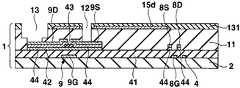
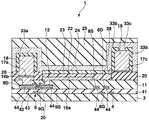
도 11∼도 16을 이용하여 제 2 실시형태에 있어서의 표시장치의 제조방법에 대하여 설명한다. 도 11∼도 16은 제조방법에 있어서의 각 공정의 단면도이고, 공정순서는 도 11∼도 16의 차례로 되어 있다. 또 도 11∼도 16에서는 제 1 실시형태에 있어서의 표시장치의 각 부에 대응하는 부분에 대하여 동일한 부호를 붙이고, 제 1 실시형태와 동일 공정 부분에 대해서는 일부 생략한다.The manufacturing method of the display apparatus in 2nd Embodiment is demonstrated using FIGS. 11-16. 11-16 is sectional drawing of each process in a manufacturing method, and the process order is in order of FIGS. 11-16. 11-16, the same code | symbol is attached | subjected about the part corresponding to each part of the display apparatus in 1st Embodiment, and the same process part as 1st Embodiment is abbreviate | omitted.

우선 도 11에 나타내는 바와 같이, 트랜지스터어레이기판(1)을 제조한다. 다음으로 평탄화막(11)상에 기상성장법 등에 의한 반사금속막(15)의 성막공정, 포토리소그래피법 등의 마스크공정, 에칭 등의 형상가공공정을 이 차례로 실시함으로써 화소마다 반사금속막(15d)을 패터 닝형성한다.First, as shown in FIG. 11, thetransistor array substrate 1 is manufactured. Next, the film forming process of thereflective metal film 15 by the vapor phase growth method or the like, the mask process such as the photolithography method, and the shape processing process such as etching are performed on theplanarizing film 11 in this order to thereby reflect thereflective metal film 15d for each pixel. Pattern).

다음으로 기상성장법을 실시함으로써 반사금속막(15d)을 피복하도록 투명절연막(131)을 전체 일면에 성막한다. 반사금속막(15d)은 투명절연막(131)에 의해서 전기적으로 절연되어 있다. 이와 같이 투명절연막(131)을 성막한 것이 제 2 실시형태와 제 1 실시형태가 다른 점이다.Next, by performing the vapor phase growth method, the transparentinsulating film 131 is formed on one surface so as to cover thereflective metal film 15d. Thereflective metal film 15d is electrically insulated by the transparentinsulating film 131. The transparentinsulating film 131 is formed in this manner in that the second embodiment differs from the first embodiment.

다음으로 포토리소그래피법, 에칭법 등을 실시함으로써 각 전류제어트랜지스터(9)의 소스(9S)에 통하는 컨택트홀(12) 및 각 전류제어트랜지스터(9)의 드레인 (9D)에 통하는 컨택트홀(13)을 평탄화막(11) 및 투명절연막(131)에 형성한다. 다음으로 질화실리콘 또는 산화실리콘으로 이루어지는 유기EL분리절연막(14)을 세로방향에 이웃한 화소의 사이에 있어서 주사선(4)과 평행하게 되도록 패터닝한다.Next, a photolithography method, an etching method, or the like is performed to contactholes 12 through thesource 9S of eachcurrent control transistor 9 and contact holes 13 through thedrain 9D of each current control transistor 9. ) Is formed in theplanarization film 11 and the transparentinsulating film 131. Next, the organic ELisolation insulating film 14 made of silicon nitride or silicon oxide is patterned so as to be parallel to thescanning line 4 between pixels adjacent to the vertical direction.

다음으로 도 12에 나타내는 바와 같이, 기상성장법에 의해서 투명금속산화물막(16)을 투명절연막(131)상의 일면에 성막한다. 투명금속산화물막(16)은 컨택트홀(12, 13) 내에 있어서도 표면에 성막되고, 전류제어트랜지스터(9)의 드레인(9D) 및 소스(9S)에 접한다. 이와 같이 반사금속막(15d)을 투명절연막(131)에 의해서 투명금속산화물막(16)과 전기적으로 분리한 것이 제 2 실시형태와 제 1 실시형태의 다른 점이다.Next, as shown in FIG. 12, the transparentmetal oxide film 16 is formed into one surface on the transparentinsulating film 131 by the vapor phase growth method. The transparentmetal oxide film 16 is formed on the surface of the contact holes 12 and 13 and is in contact with thedrain 9D and thesource 9S of thecurrent control transistor 9. In this way, thereflective metal film 15d is electrically separated from the transparentmetal oxide film 16 by the transparentinsulating film 131, which is different from the second embodiment and the first embodiment.

다음으로 스퍼터링 등의 기상성장법에 의해서 동, 니켈 등의 금속재료로 이루어지는 금속층(17)을 투명금속산화물막(16)상의 일면에 성막한다. 컨택트홀(13)과 겹치고 또한 행방향을 따른 부분의 금속층(17) 및 유기EL분리절연막(14)과 겹치며 또한 행방향을 따른 부분의 금속층(17)이 노출되는 포토레지스트막(62)을 형성한다. 또한 포토레지스트막(62)은 제 1 실시형태의 포토레지스트막(61)과 마찬가지이고, 컨택트홀(37)에서 배선(36)과 접속된 금속층(17)을 노출하며, 컨택트홀(40)에서 배선(39)과 접속된 금속층(17)을 노출하고, 또한 각 컨택트홀(46)에서 배선(45)과 접속된 금속층(17)을 노출하고 있다.Next, ametal layer 17 made of a metal material such as copper or nickel is formed on one surface on the transparentmetal oxide film 16 by a vapor phase growth method such as sputtering. Aphotoresist film 62 is formed which overlaps thecontact hole 13 and overlaps themetal layer 17 and the organic ELisolation insulating film 14 in the portion along the row direction and exposes themetal layer 17 in the portion along the row direction. do. Thephotoresist film 62 is similar to thephotoresist film 61 of the first embodiment, and exposes themetal layer 17 connected to thewiring 36 in thecontact hole 37, and in thecontact hole 40. Themetal layer 17 connected to thewiring 39 is exposed, and themetal layer 17 connected to thewiring 45 is exposed at eachcontact hole 46.

다음으로 전해도금을 실시함으로써 도 13에 나타내는 바와 같이, 노출된 금속층(17)상에 트랜지스터(7, 8, 9)의 소스, 드레인, 게이트의 막두께보다도 두꺼운 막두께 2㎛∼100㎛의 동도금후막이고 또한 5㎛∼50㎛폭의 동도금후막으로 이루어지 는 전류원라인(18) 및 EL라인(19)을 형성한다. 이에 따라 행방향으로 배열된 복수의 화소의 전류제어트랜지스터(9)의 드레인(9D)이 공통의 전류원라인(18)에 전기적으로 접속한 상태가 된다. 또한 전해도금 대신에 스퍼터링법 또는 승화증착법에 의해 동후막을 성막해도 좋다. 전류원라인(18, 18, ···) 및 EL라인(19, 19, ···)은 모두 주사선(4, 4, ···)과 동일수이고, 각 행에 전류원라인(18), EL라인(19) 및 주사선(4)이 1개씩 설치되어 있다.Next, as shown in FIG. 13, copper plating with a film thickness of 2 µm to 100 µm thicker than that of the sources, drains, and gates of thetransistors 7, 8, and 9 is performed on the exposedmetal layer 17 by electroplating. Acurrent source line 18 and anEL line 19, which are thick films and are made of a copper plated thick film having a width of 5 µm to 50 µm, are formed. As a result, thedrain 9D of thecurrent control transistors 9 of the plurality of pixels arranged in the row direction is electrically connected to the commoncurrent source line 18. Instead of electroplating, a copper thick film may be formed by sputtering or sublimation deposition. The current source lines 18, 18, ... and the EL lines 19, 19, ... are all the same number as thescan lines 4, 4, ..., and the current source lines 18, EL in each row. Theline 19 and thescanning line 4 are provided one by one.

다음으로 도 14에 나타내는 바와 같이, 포토레지스트막(62)을 제거하고 나서 전류원라인(18) 및 EL라인(19)을 마스크로 해서 노출된 금속층(17)을 에칭제거하고, 전류원라인(18, 18, ···)의 아래쪽에 밑바탕층(17a)을 형성하며, EL라인(19, 19, ···)의 아래쪽에 밑바탕층(17b)을 형성한다. 또한 투명금속산화물막(16)에 대하여 포토리소그래피법, 에칭법을 실시함으로써 화소전극(16a)을 패터닝하는 동시에, 전류원라인(18)을 마스크로 한 밑바탕층(17a)의 아래쪽에 설치된 투명금속산화물막(16)을 잔류시켜서 투명금속산화물밑바탕막(16b)을 형성하며, 밑바탕층(17b)의 아래쪽에 설치된 투명금속산화물막(16)을 잔류시켜서 투명금속산화물밑바탕막(16c)을 형성한다.Next, as shown in FIG. 14, after removing thephotoresist film 62, the exposedmetal layer 17 is etched away using thecurrent source line 18 and theEL line 19 as a mask, and thecurrent source line 18, Anunderlayer 17a is formed below 18, ..., and anunderlayer 17b is formed below the EL lines 19, 19, .... In addition, the transparentmetal oxide film 16 is subjected to photolithography and etching to pattern thepixel electrode 16a, and the transparent metal oxide provided below theunderlying layer 17a using thecurrent source line 18 as a mask. Thefilm 16 is left to form the transparent metaloxide base film 16b, and the transparent metaloxide base film 16c formed below thebase layer 17b is left to form the transparent metaloxide base film 16c.

다음으로 전류원라인(18)만을 피복하도록 전류원라인절연막(21)을 패터닝 형성한다. 그리고 도 15에 나타내는 바와 같이, PEDOT(폴리티오펜) 및 도펀트인 PSS(폴리스티렌술폰산)로 이루어지는 정공수송층(22)을 액적토출법(잉크젯법), 스핀코트법, 딥코트법, 니들에 의한 적하법 등의 습식성막법에 의해서 성막한다. 정공수송층(22)은 트랜지스터어레이기판(1)의 일면에 형성하여 모든 화소에 공통시켜 도 좋고, 화소마다 독립하도록 형성해도 좋다. 도면에서는 정공수송층(22)을 포함하는 용액 또는 현탁액이 전류원라인(18) 및 EL라인(19)에 둘러싸여진 영역에 충전된 후, 용제 또는 수분이 휘발함으로써 정공수송층(22)이 성막되어 있는 상태를 나타내고 있다.Next, the current sourceline insulating film 21 is patterned to cover only thecurrent source line 18. And as shown in FIG. 15, the hole-transport layer 22 which consists of PEDOT (polythiophene) and a dopant PSS (polystyrene sulfonic acid) is dripped by the droplet ejection method (inkjet method), the spin coat method, the dip coat method, and the needle. The film is formed by a wet film formation method such as a method. Thehole transport layer 22 may be formed on one surface of thetransistor array substrate 1 to be common to all the pixels, or may be formed so as to be independent for each pixel. In the figure, the solution or suspension including thehole transport layer 22 is filled in the region surrounded by thecurrent source line 18 and theEL line 19, and then the solvent or water is volatilized to form thehole transport layer 22. Indicates.

정공수송층(22)의 건조 후, 제 1 실시형태와 마찬가지로 폴리플루오렌계 발광재료로 이루어지는 발광층(23)을 액적토출법(잉크젯법), 니들에 의한 적하법 등의 습식성막법에 의해서 화소마다 패터닝한다. 여기에서 유기EL분리절연막(14)의 위에 투명금속산화물밑바탕막(16c), 밑바탕층(17b) 및 EL라인(19)이 잔류하고 있는데, 정공수송층(22)의 막두께나 발광층(23)의 막두께는 유기EL분리절연막(14)의 막두께보다도 얇다. 그리고 정공수송층(22)이 되는 용액 또는 현탁액의 높이 및 화소영역에 피복했을 때의 발광층(23)이 되는 용액 또는 현탁액의 높이는 모두 전류원라인(18)의 높이나 EL라인(19)의 높이 보다도 낮다. 따라서 정공수송층(22)이 되는 용액 또는 현탁액 및 발광층(23)이 되는 용액 또는 현탁액은 전류원라인(18) 및 EL라인(19)을 넘어서 이웃한 행의 화소에 유출하는 일은 없다. 이와 같이 전류원라인(18) 및 EL라인(19)은 정공수송층(22)이 되는 용액 또는 현탁액 및 발광층(23)이 되는 용액 또는 현탁액의 유출을 방지하는 격벽으로서 기능한다. 따라서 도 9에 나타내는 바와 같이, 전류원라인(18) 및 EL라인(19)을 따라서 둘러싸여진 행방향의 복수의 화소는 동일색으로 발광하는 발광층으로 하면 전류원라인(18) 및 EL라인(19)간에 일괄하여 발광층(23)을 포함하는 용액 또는 현탁액을 유입시킴으로써 행방향의 복수의 화소에 발광층(23)을 일괄하여 성막할 수 있다.After drying thehole transport layer 22, thelight emitting layer 23 made of a polyfluorene-based light emitting material is subjected to a wet film formation method such as a droplet ejection method (ink jet method) or a dropping method using a needle in the same manner as in the first embodiment. Pattern. Here, the transparentmetal oxide underlayer 16c, theunderlayer 17b, and theEL line 19 remain on the organic ELisolation insulating film 14, and the film thickness of thehole transport layer 22 and thelight emitting layer 23 The film thickness is thinner than that of the organic ELisolation insulating film 14. The height of the solution or suspension serving as thehole transport layer 22 and the height of the solution or suspension serving as thelight emitting layer 23 when the pixel region is coated are lower than the height of thecurrent source line 18 and the height of theEL line 19. Therefore, the solution or suspension serving as thehole transport layer 22 and the solution or suspension serving as thelight emitting layer 23 do not flow over thecurrent source line 18 and theEL line 19 to the pixels in the adjacent rows. In this way, thecurrent source line 18 and theEL line 19 function as partition walls for preventing the outflow of the solution or suspension serving as thehole transport layer 22 and the solution or suspension serving as thelight emitting layer 23. Therefore, as shown in FIG. 9, when the plurality of pixels in the row direction surrounded by thecurrent source line 18 and theEL line 19 are light emitting layers emitting light of the same color, between thecurrent source line 18 and theEL line 19. By injecting the solution or suspension containing thelight emitting layer 23 collectively, thelight emitting layer 23 can be collectively formed into a some pixel of a row direction.

다음으로 도 16에 나타내는 바와 같이, 증착 등의 기상성장법에 의해서 마그네슘, 칼슘, 리튬, 바륨, 희토류금속 등의 낮은 일함수재료로 이루어지는 전자주입층과, 산화인듐, 산화아연 혹은 산화주석 또는 이들 중의 적어도 하나를 포함하는 혼합물(예를 들면, 주석도프산화인듐(ITO), 아연도프산화인듐, 카드뮴-주석산화물(CTO))을 갖는 투명도전층과의 이층구조의 공통전극(24)을 캐소드전극으로서 일면에 성막한다. 전자주입층은 10nm∼200nm의 두께로 가시광이 투과할 정도로 얇기 때문에 전류원라인(18)이나 EL라인(19)의 단차에 의해서 절단되어도 좋지만, 공통전극(24)의 투명도전층은 복수의 화소의 유기EL소자(26)의 한쪽의 전극을 서로 등전위로 하기 위해 전류원라인(18)상의 전류원라인절연막(21)의 위를 넘고 또한 EL라인(19)상에 걸치도록 성막되어 있다. 이에 따라 발광층(23)은 공통전극(24)에 밀착한 상태에서 공통전극(24)에 의해서 피복되고, 또한 EL라인(19)도 공통전극(24)에 밀착한 상태에서 공통전극(24)에 의해서 피복되어 유기EL소자(26)가 성막된다.Next, as shown in FIG. 16, the electron injection layer which consists of low work function materials, such as magnesium, calcium, lithium, barium, and rare earth metals by vapor phase growth methods, such as vapor deposition, indium oxide, zinc oxide, or tin oxide, or these The cathode electrode is formed of acommon electrode 24 having a two-layer structure with a transparent conductive layer having a mixture containing at least one of (e.g., indium tin dope oxide (ITO), indium zinc dope oxide, and cadmium-tin oxide (CTO)). As a film is formed on one side. Since the electron injection layer is thin enough to transmit visible light with a thickness of 10 nm to 200 nm, it may be cut by the step of thecurrent source line 18 or theEL line 19, but the transparent conductive layer of thecommon electrode 24 is formed of organic materials of a plurality of pixels. One electrode of theEL element 26 is formed over the current sourceline insulating film 21 on thecurrent source line 18 and over theEL line 19 so as to equipotentially. Accordingly, thelight emitting layer 23 is covered by thecommon electrode 24 in a state of being in close contact with thecommon electrode 24, and theEL line 19 is also in contact with thecommon electrode 24 in the state of being in close contact with thecommon electrode 24. Theorganic EL element 26 is deposited to form a film.

다음으로 스핀코트법, 딥코트법, 기상성장법에 의해서 오버코트절연층(25)을 일면에 성막하고, 주사드라이버(32), 데이터드라이버(33) 및 전류원드라이버(34)를 접속하고 나서 투명밀봉기판을 맞붙인다.Next, theovercoat insulating layer 25 is formed on one surface by the spin coating method, the dip coating method, and the vapor phase growth method, and thescan driver 32, thedata driver 33, and thecurrent source driver 34 are connected, and then transparently sealed. Glue the substrate.

이상에 의해 액티브매트릭스 구동방식의 일렉트로루미네선트 디스플레이패널이 완성된다.The electroluminescent display panel of the active matrix drive system is completed by the above.

제 2 실시형태에 있어서도 전류원라인(18) 및 EL라인(19)을 트랜지스터(7, 8, 9)의 일부를 구성하는 도전막과는 다른 막으로 형성되어 있기 때문에 전류원라 인(18) 및 EL라인(19)을 트랜지스터(7, 8, 9)의 드레인, 소스, 게이트나 신호전류선(3), 주사선(4) 등보다도 후막으로 하여 단위길이당의 저항을 보다 작게 할 수 있다. 그 때문에 전류원라인(18)이나 EL라인(19)의 전기저항을 낮게 할 수 있고, 발광기간의 개시시로부터 유기EL소자(26)가 소망의 밝기(계조)로 발광하기까지의 시간의 지연을 억제하거나, 전류원라인(18)이나 EL라인(19)에 있어서의 전압강하를 억제하거나 할 수 있다. 또한 전류원라인(18)이나 EL라인(19)을 저저항으로 함으로써 일렉트로루미네선트 디스플레이패널의 밝기의 저하, 밝기의 불균형, 크로스토크 등의 표시악화를 억제할 수 있다.Also in the second embodiment, since thecurrent source line 18 and theEL line 19 are formed of a different film from the conductive film forming part of thetransistors 7, 8, and 9, the current source lines 18 and the EL lines 19 are formed. The resistance per unit length can be made smaller by using theline 19 as a thicker film than the drains, sources, gates, signalcurrent lines 3,scan lines 4, etc. of thetransistors 7, 8, 9, and the like. Therefore, the electrical resistance of thecurrent source line 18 and theEL line 19 can be lowered, and the delay of the time from the start of the light emission period until theorganic EL element 26 emits light at a desired brightness (gradation) can be reduced. The voltage drop in thecurrent source line 18 or theEL line 19 can be suppressed. In addition, by making thecurrent source line 18 and the EL line 19 a low resistance, it is possible to suppress display deterioration such as lowering of brightness, unbalance of brightness, crosstalk, etc. of the electroluminescent display panel.

<제 3 실시형태>Third Embodiment

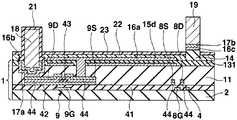
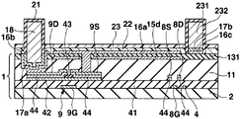
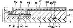
도 17∼도 22를 이용하여 제 3 실시형태에 있어서의 일렉트로루미네선트 디스플레이패널의 제조방법에 대하여 설명한다. 도 17∼도 22는 제조방법에 있어서의 각 공정의 단면도이고, 공정순서는 도 17∼도 22의 차례로 되어 있다. 또 도 17∼도 22에서는 제 2 실시형태에 있어서의 일렉트로루미네선트 디스플레이패널의 각 부에 대응하는 부분에 대하여 동일한 부호를 붙이고, 제 1 실시형태와 동일 공정 부분에 대해서는 일부 생략한다.The manufacturing method of the electroluminescent display panel in 3rd Embodiment is demonstrated using FIGS. 17-22. 17-22 is sectional drawing of each process in the manufacturing method, and the process order is in order of FIG. 17-22. 17-22, the same code | symbol is attached | subjected about the part corresponding to each part of the electroluminescent display panel in 2nd Embodiment, and the same process part as 1st Embodiment is abbreviate | omitted.

우선 도 17에 나타내는 바와 같이, 트랜지스터어레이기판(1)을 제조한다. 다음으로 평탄화막(11)상에 스토퍼 등의 기상성장법에 의한 반사금속막의 성막공정, 포토리소그래피법 등의 마스크공정, 에칭 등의 형상가공공정을 이 차례로 실시함으로써 화소마다 반사금속막(15d)을 패터닝 형성한다.First, as shown in FIG. 17, thetransistor array substrate 1 is manufactured. Next, on theplanarization film 11, a film forming process of a reflective metal film by a vapor phase growth method such as a stopper, a mask process such as a photolithography method, and a shape processing process such as etching are performed in this order so that thereflective metal film 15d for each pixel To form a patterning.

다음으로 기상성장법을 실시함으로써 반사금속막(15d)를 피복하도록 투명절 연막(131)을 전체 일면에 성막한다. 반사금속막(15d)은 투명절연막(131)에 의해서 전기적으로 절연되어 있다.Next, by performing the vapor phase growth method, the transparentinsulating film 131 is formed on one surface so as to cover thereflective metal film 15d. Thereflective metal film 15d is electrically insulated by the transparentinsulating film 131.

다음으로 포토리소그래피법, 에칭법 등을 실시함으로써 각 전류제어트랜지스터(9)의 소스(9S)에 통하는 컨택트홀(12) 및 각 전류제어트랜지스터(9)의 드레인(9D)에 통하는 컨택트홀(13)을 평탄화막(11) 및 투명절연막(131)에 형성한다.Next, a photolithography method, an etching method, or the like is performed to contactholes 12 through thesource 9S of eachcurrent control transistor 9 and contact holes 13 through thedrain 9D of each current control transistor 9. ) Is formed in theplanarization film 11 and the transparentinsulating film 131.

여기에서 제 2 실시형태에서는 유기EL분리절연막(14)을 패터닝했는데, 본 실시형태에서는 유기EL분리절연막을 패터닝하지 않는다.Here, in the second embodiment, the organic ELisolation insulating film 14 is patterned, but in the present embodiment, the organic EL isolation insulating film is not patterned.

다음으로 도 18에 나타내는 바와 같이, 기상성장법에 의해서 투명금속산화물막(16)을 투명절연막(131)상의 일면에 성막한다. 투명금속산화물막(16)은 투명금속산화물막(16)은 컨택트홀(12, 13) 내에 있어서도 표면에 성막되고, 전류제어트랜지스터(9)의 드레인(9D) 및 소스(9S)에 접한다.Next, as shown in FIG. 18, the transparentmetal oxide film 16 is formed into one surface on the transparentinsulating film 131 by the vapor phase growth method. The transparentmetal oxide film 16 is formed on the surface of the transparentmetal oxide film 16 in the contact holes 12 and 13 and is in contact with thedrain 9D and thesource 9S of thecurrent control transistor 9.

다음으로 도 19에 나타내는 바와 같이, 기상성장법에 의해서 동, 니켈 등의 금속재료로 이루어지는 금속층(17)을 투명금속산화물막(16)상의 일면에 성막한다. 금속층(17)에 있어서의 컨택트홀(13)과 겹치고 또한 행방향을 따른 부분(17a) 및 반사금속막(15d)에 대하여 부분(17a)과 대향하는 변측(邊側)에 행방향을 따른 격벽(231)이 형성되는 부분(17b)이 노출되는 포토레지스트막(63)을 형성한다. 또한 포토레지스트막(63)은 제 1 실시형태의 포토레지스트막(61)과 마찬가지로 컨택트홀(37)에서 배선(36)과 접속된 금속층(17)을 노출하고, 컨택트홀(40)에서 배선(39)과 접속된 금속층(17)을 노출하며, 또한 각 컨택트홀(46)에서 배선(45)과 접속된 금속층(17)을 노출하고 있다.Next, as shown in FIG. 19, themetal layer 17 which consists of metal materials, such as copper and nickel, is formed into a film on the transparentmetal oxide film 16 by the vapor phase growth method. The partition wall which overlaps with thecontact hole 13 in themetal layer 17 and along the row direction on theside 17a which faces thepart 17a and thereflective metal film 15d along the row direction and faces thepart 17a. Aphotoresist film 63 through which theportion 17b where 231 is formed is exposed is formed. Similarly to thephotoresist film 61 of the first embodiment, thephotoresist film 63 exposes themetal layer 17 connected to thewiring 36 in thecontact hole 37 and the wiring (in the contact hole 40). Themetal layer 17 connected to 39 is exposed, and themetal layer 17 connected to thewiring 45 is exposed at eachcontact hole 46.

다음으로 전해도금을 실시함으로써 노출된 밑바탕층(17a 17b)상에 트랜지스터(7, 8, 9)의 소스, 드레인, 게이트의 막두께보다도 두꺼운 막두께 2㎛∼100㎛, 5㎛∼50㎛폭의 동도금후막으로 이루어지는 전류원라인(18) 및 격벽(231)을 형성한다. 이에 따라 행방향으로 배열된 복수의 화소의 전류제어트랜지스터(9)의 드레인(9D)이 공통의 전류원라인(18)에 전기적으로 접속한 상태가 된다. 또한 전해도금 대신에 스퍼터링법 또는 승화증착법에 의해 동후막을 성막해도 좋다.Next, the film thickness of 2 μm to 100 μm and 5 μm to 50 μm wider than the thickness of the source, drain, and gate of thetransistors 7, 8, and 9 on theunderlying layer 17a 17b exposed by electroplating. Acurrent source line 18 and apartition wall 231 made of a copper plated thick film are formed. As a result, thedrain 9D of thecurrent control transistors 9 of the plurality of pixels arranged in the row direction is electrically connected to the commoncurrent source line 18. Instead of electroplating, a copper thick film may be formed by sputtering or sublimation deposition.

또한 전류원라인(18, 18, ···) 및 격벽(231, 231, ···)을 패터닝함에 있어서 전류원라인(18)을 격벽(231)에 대하여 평행하게 설치하고, 또한 전류원라인(18) 및 격벽(231)을 주사선(4)에 대하여 평행하게 설치한다. 또 평면에서 보아 가로방향(행방향)으로 배열된 모든 화소의 컨택트홀(13)에 대하여 전류원라인(18)이 겹치도록 전류원라인(18)을 패터닝한다. 또한 전류원라인(18)을 트랜지스터어레이기판(1)의 테두리까지 연장하도록 전류원라인(18)을 패터닝한다.Further, in patterning the current source lines 18, 18,... And thepartition walls 231, 231,..., The current source lines 18 are provided in parallel with thepartition walls 231, and the current source lines 18 are also provided. And thepartition wall 231 is provided parallel to thescan line 4. In addition, thecurrent source line 18 is patterned so that thecurrent source line 18 overlaps the contact holes 13 of all the pixels arranged in the horizontal direction (row direction) in plan view. In addition, thecurrent source line 18 is patterned to extend thecurrent source line 18 to the edge of thetransistor array substrate 1.

다음으로 도 20에 나타내는 바와 같이, 포토레지스트막(63)을 제거하고 나서 전류원라인(18) 및 격벽(231)을 마스크로 해서 노출된 금속층(17)을 에칭제거하고, 전류원라인(18, 18, ···)의 아래쪽에 밑바탕층(17a)을 잔존하며, 격벽(231, 231, ···)의 아래쪽에 밑바탕층(17b)을 잔존한다. 또한 투명금속산화물막(16)에 대하여 포토리소그래피법, 에칭법을 실시함으로써 화소전극(16a)을 패터닝하는 동시에, 전류원라인(18)을 마스크로 한 밑바탕층(17a)의 아래쪽에 설치된 투명금속산화물막(16)을 잔류시켜서 투명금속산화물밑바탕막(16b)을 형성하며, 밑바탕층(17b)의 아래쪽에 설치된 투명금속산화물막(16)을 잔류시켜서 투명금속산화물밑바 탕막(16c)을 형성한다.Next, as shown in FIG. 20, after removing thephotoresist film 63, the exposedmetal layer 17 is etched away using thecurrent source line 18 and thepartition 231 as a mask, and the current source lines 18 and 18 are then removed. Thebottom layer 17a remains below the bottom, and thebottom layer 17b remains below thepartitions 231, 231,. In addition, the transparentmetal oxide film 16 is subjected to photolithography and etching to pattern thepixel electrode 16a, and the transparent metal oxide provided below theunderlying layer 17a using thecurrent source line 18 as a mask. Thefilm 16 is left to form the transparent metaloxide base film 16b, and the transparent metaloxide base film 16c formed below thebase layer 17b is left to form the transparent metaloxide base film 16c.

다음으로 도 21에 나타내는 바와 같이, 전류원라인(18)을 피복하도록 전류원라인절연막(21)을 형성하는 동시에, 격벽(231)을 피복하도록 전류원라인절연막(21)과 같은 재료의 EL라인절연막(232)을 전류원라인절연막(21)과 동일 공정에서 형성한다. 이상에 의해 유기EL구동기판이 완성된다.Next, as shown in FIG. 21, the current sourceline insulating film 21 is formed to cover thecurrent source line 18, and the ELline insulating film 232 of the same material as the current sourceline insulating film 21 to cover the partition wall 231. ) Is formed in the same process as the current sourceline insulating film 21. The organic EL driving substrate is completed by the above.

다음으로 PEDOT(폴리티오펜) 및 도펀트인 PSS(폴리스티렌술폰산)으로 이루어지는 정공수송층(22)을 액적토출법(잉크젯법), 스핀코트법, 딥코트법, 니들에 의한 적하법 등의 습식성막법에 의해서 성막한다. 정공수송층(22)은 트랜지스터어레이기판(1)의 일면에 형성하여 모든 화소에 공통시켜도 좋고, 화소마다 독립하도록 형성해도 좋다. 도면에서는 정공수송층(22)을 포함하는 용액 또는 현탁액이 전류원라인(18) 및 격벽(231)에 둘러싸여진 영역에 충전된 후, 용제 또는 수분이 휘발함으로써 정공수송층(22)이 성막된 상태를 나타내고 있다.Next, the wet-transporting method of thehole transport layer 22 made of PEDOT (polythiophene) and dopant PSS (polystyrene sulfonic acid) is a liquid film deposition method such as a droplet ejection method (ink jet method), spin coating method, dip coating method, dropping method by needle, etc. Formation by Thehole transport layer 22 may be formed on one surface of thetransistor array substrate 1 to be common to all the pixels, or may be formed so as to be independent for each pixel. In the drawing, after the solution or suspension including thehole transport layer 22 is filled in a region surrounded by thecurrent source line 18 and thepartition wall 231, thehole transport layer 22 is formed by volatilizing a solvent or water. have.

정공수송층(22)의 건조 후, 제 1 실시형태와 마찬가지로 폴리플루오렌계 발광재료로 이루어지는 발광층(23)을 액적토출법(잉크젯법), 니들에 의한 적하법 등의 습식성막법에 의해서 화소마다 패터닝한다. 여기에서 정공수송층(22)의 막두께나 발광층(23)의 막두께는 격벽(231)의 막두게보다도 얇다. 그리고 정공수송층(22)이 되는 용액 또는 현탁액의 높이 및 화소영역에 피복했을 때의 발광층(23)이 되는 용액 또는 현탁액의 높이는 전류원라인(18)의 높이나 격벽(231)의 높이보다도 낮다. 따라서 정공수송층(22)이 되는 용액 또는 현탁액 및 발광층(23)이 되는 용액 또는 현탁액은 전류원라인(18) 및 격벽(231)을 넘어서 이웃한 행의 화소에 유출 하는 일은 없다. 이와 같이 전류원라인(18) 및 격벽(231)은 정공수송층(22)이 되는 용액 또는 현탁액 및 발광층(23)이 되는 용액 또는 현탁액의 유출을 방지하는 격벽으로서 기능한다. 따라서 전류원라인(18) 및 격벽(231)을 따라서 둘러싸여진 행방향의 복수의 화소는 동일색으로 발광하는 발광층으로 하면 전류원라인(18) 및 격벽(231)간에 일괄하여 발광층(23)을 포함하는 용액 또는 현탁액을 유입시킴으로써 행방향의 복수의 화소로 발광층(23)을 일괄하여 성막할 수 있다.After drying thehole transport layer 22, thelight emitting layer 23 made of a polyfluorene-based light emitting material is subjected to a wet film formation method such as a droplet ejection method (ink jet method) or a dropping method using a needle in the same manner as in the first embodiment. Pattern. Here, the film thickness of thehole transport layer 22 and the film thickness of thelight emitting layer 23 are thinner than the film thickness of thepartition wall 231. The height of the solution or suspension serving as thehole transport layer 22 and the height of the solution or suspension serving as thelight emitting layer 23 when the pixel region is coated are lower than the height of thecurrent source line 18 and the height of thepartition wall 231. Therefore, the solution or suspension serving as thehole transport layer 22 and the solution or suspension serving as thelight emitting layer 23 do not flow over thecurrent source line 18 and thepartition wall 231 to the pixels in the adjacent rows. Thus, thecurrent source line 18 and thepartition wall 231 function as a partition wall which prevents the outflow of the solution or suspension which becomes thehole transport layer 22, and the solution or suspension which becomes thelight emitting layer 23. As shown in FIG. Accordingly, when the plurality of pixels in the row direction surrounded by thecurrent source line 18 and thepartition wall 231 are light emitting layers emitting light of the same color, thelight emitting layer 23 may be collectively included between thecurrent source line 18 and thepartition wall 231. By injecting a solution or a suspension, thelight emitting layer 23 can be collectively formed into a plurality of pixels in the row direction.

다음으로 도 22에 나타내는 바와 같이, 증착 등의 기상성장법에 의해서 마그네슘, 칼슘, 리튬, 바륨, 희토류금속 등의 낮은 일함수의 재료로 이루어지는 전자주입층과, 산화인듐, 산화아연 혹은 산화주석 또는 이들 중의 적어도 하나를 포함하는 혼합물(예를 들면, 주석도프산화인듐(ITO), 아연도프산화인듐, 카드뮴-주석산화물(CTO))을 갖는 투명도전층과의 이층구조의 공통전극(24)을 캐소드전극으로서 일면에 성막한다. 전자주입층은 10nm∼200nm의 두께로 가시광이 투과할 정도로 얇기 때문에 전류원라인(18)이나 격벽(231)의 격차에 의해서 절단되어도 좋지만, 공통전극(24)의 투명도전층은 복수의 화소의 유기EL소자(26)의 한쪽의 전극을 서로 등전위로 하기 위해 전류원라인(18)표면의 전류원라인절연막(21)상에 넘고 또한 격벽(231)표면의 EL라인절연막(232)상에 걸치도록 성막되어 있다. 이에 따라 발광층(23)은 공통전극(24)에 밀착한 상태로 공통전극(24)에 의해서 피복되고, 또한 격벽(231)도 공통전극(24)에 밀착한 상태로 공통전극(24)에 의해서 피복되어 유기EL소자(26)가 형성된다. 격벽(231)은 정공수송층(22)을 포함하는 용액 또는 현탁액 및/또는 발광층(23)을 포함하는 용액 또는 현탁액을 소정의 위치에 설치하기 위한 칸 막이로서 이용함에 있어서, 제 1 실시형태의 EL라인(19)과 같이 전압이 인가되어 있는 것은 아니다.Next, as shown in FIG. 22, the electron injection layer which consists of materials of low work function, such as magnesium, calcium, lithium, barium, and rare earth metals by vapor phase growth methods, such as vapor deposition, indium oxide, zinc oxide, or tin oxide, or Cathode acommon electrode 24 of a two-layer structure with a transparent conductive layer having a mixture containing at least one of them (e.g., indium tin dope oxide (ITO), indium zinc dope oxide, cadmium-tin oxide (CTO)). It is formed on one surface as an electrode. Since the electron injection layer is thin enough to transmit visible light with a thickness of 10 nm to 200 nm, it may be cut by the gap between thecurrent source line 18 and thepartition wall 231, but the transparent conductive layer of thecommon electrode 24 is formed of organic EL of a plurality of pixels. One electrode of theelement 26 is formed so as to pass over the current sourceline insulating film 21 on the surface of thecurrent source line 18 and across the ELline insulating film 232 on the surface of thepartition wall 231 so as to equipotentially. . Accordingly, thelight emitting layer 23 is covered by thecommon electrode 24 while being in close contact with thecommon electrode 24, and thepartition wall 231 is also in contact with thecommon electrode 24 by thecommon electrode 24. Theorganic EL element 26 is formed by covering. Thepartition wall 231 serves as a partition for installing a solution or suspension containing thehole transport layer 22 and / or a solution or suspension containing thelight emitting layer 23 in a predetermined position, and according to the EL of the first embodiment. Likeline 19, no voltage is applied.

다음으로 증착법, 스퍼터링법, 스크린인쇄법, 승화증착법, 디스펜서법 등에 의해서 평면에서 보아 격벽(231)에 겹치도록 트랜지스터(7, 8, 9)의 소스, 드레인, 게이트의 막두께보다도 두꺼운 막두께의 EL라인(233)을 공통전극(24)상에 형성한다. EL라인(233)은 제 1 실시형태의 EL라인(19)에 상당하는 것으로, 형상, 길이, 두께 모두 EL라인(19)과 마찬가지이고, 트랜지스터(7, 8, 9)의 소스(7S, 8S, 9S), 드레인(7D, 8D, 9D), 게이트(7G, 8G, 9G)의 막두께보다도 두껍기 때문에 이들 전극보다도 단위배선의 길이당의 저항이 낮게 설정되어 있다. 또 EL라인(233)은 제 1 실시형태의 EL라인(19)과 마찬가지로 포토레지스트막(61)을 이용하여 전해도금에 의해 퇴적되어도 좋다. EL라인(233)은 격벽(231) 위쪽에 있어서 전체 화소공통의 공통전극(24)과 접속되어 있다. 전류원라인(18, 18, ···) 및 EL라인(233, 233, ···)은 모두 주사선(4, 4, ···)과 동일수이고, 각 행에 전류원라인(18), EL라인(233) 및 주사선(4)이 1개씩 설치되어 있다.Next, a film thickness thicker than that of the source, drain, and gate of thetransistors 7, 8, and 9 so as to overlap thepartition wall 231 in plan view by vapor deposition, sputtering, screen printing, sublimation deposition, dispenser, or the like. AnEL line 233 is formed on thecommon electrode 24. TheEL line 233 corresponds to theEL line 19 of the first embodiment, and the shape, the length, and the thickness are the same as those of theEL line 19, and thesources 7S and 8S of thetransistors 7, 8, and 9 are shown. , 9S), drains 7D, 8D, 9D, and thicker than the film thicknesses ofgates 7G, 8G, and 9G, the resistance per unit wiring length is set lower than those of these electrodes. TheEL line 233 may be deposited by electroplating using thephotoresist film 61 similarly to theEL line 19 of the first embodiment. TheEL line 233 is connected to thecommon electrode 24 of all the pixels common above thepartition 231. The current source lines 18, 18, ... and the EL lines 233, 233, ... are all the same number as thescan lines 4, 4, ..., and the current source lines 18, EL in each row. Thelines 233 and thescanning lines 4 are provided one by one.

다음으로 스핀코트법, 딥코트법, 기상성장법에 의해서 오버코트절연층(25)을 일면에 성막하고, 주사드라이버(32), 데이터드라이버(33) 및 전류원드라이버(34)를 접속하고 나서 투명밀봉기판을 맞붙인다.Next, theovercoat insulating layer 25 is formed on one surface by the spin coating method, the dip coating method, and the vapor phase growth method, and thescan driver 32, thedata driver 33, and thecurrent source driver 34 are connected, and then transparently sealed. Glue the substrate.

이상에 의해 액티브매트릭스 구동방식의 표시장치가 완성된다.This completes the display of the active matrix drive system.

제 3 실시형태에 있어서도 전류원라인(18) 및 EL라인(233)을 트랜지스터(7, 8, 9)의 일부를 구성하는 도전막과는 다른 막으로 형성되어 있기 때문에 전류원라 인(18) 및 EL라인(233)을 트랜지스터(7, 8, 9)의 드레인, 소스, 게이트나 신호전류선(3), 주사선(4) 등보다도 후막으로 할 수 있다. 그 때문에 전류원라인(18)이나 EL라인(233)의 전기저항을 낮게 할 수 있고, 발광기간의 개시시로부터 유기EL소자(26)가 소망의 밝기(계조)로 발광하기까지의 시간의 지연을 억제하거나, 전류원라인(18)이나 EL라인(233)에 있어서의 전압강하를 억제하거나 할 수 있다. 또한 전류원라인(18)이나 EL라인(233)을 저저항으로 함으로써 일렉트로루미네선트 디스플레이패널의 밝기의 저하, 밝기의 불균형, 크로스토크 등의 표시악화를 억제할 수 있다.Also in the third embodiment, since thecurrent source line 18 and theEL line 233 are formed of a different film from the conductive film forming part of thetransistors 7, 8 and 9, the current source lines 18 and the EL lines are formed. Theline 233 can be made thicker than the drain, source, gate, signalcurrent line 3,scan line 4, or the like of thetransistors 7, 8, 9. Therefore, the electrical resistance of thecurrent source line 18 or theEL line 233 can be lowered, and the delay of the time from the start of the light emission period until theorganic EL element 26 emits light at a desired brightness (gradation) can be reduced. The voltage drop in thecurrent source line 18 or theEL line 233 can be suppressed. Further, by setting thecurrent source line 18 and theEL line 233 to low resistances, it is possible to suppress display deterioration such as lowering of brightness of the electroluminescent display panel, unbalance of brightness, crosstalk, and the like.

<제 4 실시형태>Fourth Embodiment

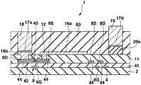
도 23∼도 28을 이용하여 제 4 실시형태에 있어서의 일렉트로루미네선트 디스플레이패널의 제조방법에 대해서 설명한다. 도 23∼도 28은 제조방법에 있어서의 각 공정의 단면도이고, 공정순서는 도 23∼도 28의 차례로 되어 있다. 또 도 23∼도 28에서는 제 1 실시형태에 있어서의 일렉트로루미네선트 디스플레이패널의 각 부에 대응하는 부분에 대하여 동일한 부호를 붙이고, 제 1 실시형태와 동일 공정 부분에 대해서는 일부 생략한다.The manufacturing method of the electroluminescent display panel in 4th Embodiment is demonstrated using FIGS. 23-28. 23-28 is sectional drawing of each process in a manufacturing method, and the process order is in order of FIG. 23-28. 23-28, the same code | symbol is attached | subjected about the part corresponding to each part of the electroluminescent display panel in 1st Embodiment, and abbreviate | omits a part about the same process part as 1st Embodiment.

우선 도 23에 나타내는 바와 같이, 트랜지스터어레이기판(1)을 제조한다. 준비한 트랜지스터어레이기판(1)에 대해서 포토리소그래피법, 에칭법 등을 실시함으로써 각 전류제어트랜지스터(9)의 소스(9S)에 통하는 콘택트홀(12) 및 각 전류제어트랜지스터(9)의 드레인(9D)에 통하는 컨택트홀(13)을 평탄화막(11)에 형성한다.First, as shown in FIG. 23, thetransistor array substrate 1 is manufactured. A photolithography method, an etching method, or the like is performed on the preparedtransistor array substrate 1 to contact 9 through thesource 9S of eachcurrent control transistor 9 and thedrain 9D of eachcurrent control transistor 9. Acontact hole 13 through) is formed in theplanarization film 11.

다음으로 질화실리콘 또는 산화실리콘으로 이루어지는 유기EL분리절연막(14) 을 세로(열)방향에 이웃한 화소의 사이에 있어서 주사선(4)과 평행하게 되도록 패터닝하여 형성한다.Next, an organic ELisolation insulating film 14 made of silicon nitride or silicon oxide is patterned so as to be parallel to thescanning line 4 between pixels adjacent in the vertical (column) direction.

다음으로 도 24에 나타내는 바와 같이, 기상성장법에 의해서 투명금속산화물막(16)을 트랜지스터어레이기판(1)상의 일면에 성막한다. 여기에서 제 1 실시형태에서는 투명금속산화물막(16)의 앞에 반사금속막(15)을 성막했는데, 본 실시형태에서는 반사금속막(15)을 성막하지 않는다. 다음으로 기상성장법에 의해서 동, 니켈 등의 금속재료로 이루어지는 금속층(17)을 투명금속산화물막(16)상의 일면에 성막한다.Next, as shown in FIG. 24, the transparentmetal oxide film 16 is formed into a film on one surface of thetransistor array substrate 1 by a vapor phase growth method. Here, in the first embodiment, thereflective metal film 15 is formed in front of the transparentmetal oxide film 16. In the present embodiment, thereflective metal film 15 is not formed. Next, ametal layer 17 made of a metal material such as copper or nickel is formed on one surface on the transparentmetal oxide film 16 by the vapor phase growth method.

다음으로 포토리소그래피법에 의해 마스크를 패터닝하고, 증착법 등의 방법으로 금의 박막을 성막하며, 마스크를 박리함으로써 금박막으로 이루어지는 화소전극(331)을 형성한다. 또한 화소전극(331)을 패터닝함에 있어서 상기 마스크는 후술하는 전류원라인(18)에 대응하는 부분, 즉 컨택트홀(13)과 겹치고 또한 행방향으로 연장한 부분 및 EL라인(19)에 대응하는 부분, 즉 유기EL분리절연막(14)과 겹치며 또한 행방향으로 연장한 부분에 각각 밑바탕막(331a, 331b)이 잔존하는 마스크이다.Next, a mask is patterned by a photolithography method, a thin film of gold is formed by a deposition method or the like, and thepixel electrode 331 made of a gold thin film is formed by peeling the mask. In the patterning of thepixel electrode 331, the mask corresponds to a portion corresponding to thecurrent source line 18 described later, that is, a portion overlapping thecontact hole 13 and extending in the row direction and corresponding to theEL line 19. In other words, the underlyingfilms 331a and 331b remain in portions overlapping the organic ELisolation insulating film 14 and extending in the row direction, respectively.

다음으로 도 25에 나타내는 바와 같이, 컨택트홀(13)과 겹치고 또한 행방향을 따른 부분의 밑바탕막(331a) 및 유기EL분리절연막(14)과 겹치며 또한 행방향을 따른 부분의 밑바탕막(331b)이 노출되는 포토레지스트막(64)을 형성한다. 계속해서 노출된 밑바탕막(331a) 및 밑바탕막(331b)을 전극으로서 전해도금을 실시함으로써 밑바탕막(331a) 및 밑바탕막(331b)상에 각각 막두께 2㎛∼100㎛ 또한 5㎛∼50㎛ 폭의 동도금후막의 전류원라인(18) 및 EL라인(19)을 형성한다. 전류원라인(18, 18, ···) 및 EL라인(19, 19, ···)은 트랜지스터(7, 8, 9)의 소스(7S, 8S, 9S), 드레인(7D, 8D, 9D), 게이트(7G, 8G, 9G)의 막두께보다도 두껍게 퇴적되어 있기 때문에 이들 전극보다도 단위배선의 길이당의 저항이 낮게 설정되어 있다. 전류원라인(18, 18, ···) 및 EL라인(19, 19, ···)은 모두 주사선(4, 4, ···)과 동일수이고, 각 행에 전류원라인(18), EL라인(19) 및 주사선(4)이 1개씩 설치되어 있다. 이 후, 포토레지스트막(64)을 제거한다. 또한 전해도금 대신에 스퍼터링법, 승화증착법 또는 디스펜서법에 의해 동두께막을 성막해도 좋다.Next, as shown in FIG. 25, thebase film 331b of the part which overlaps with thecontact hole 13 and along the row direction, and thebase EL film 331b of the part which overlaps with the organic ELisolation insulating film 14 and along the row direction is also shown. The exposedphotoresist film 64 is formed. Subsequently, electroplating is performed using the exposedbase film 331a and thebase film 331b as electrodes, and the film thicknesses of 2 μm to 100 μm and 5 μm to 50 μm on thebase film 331a and thebase film 331b, respectively. Thecurrent source line 18 and theEL line 19 of the copper plating thick film of the width | variety are formed. The current source lines 18, 18, ... and the EL lines 19, 19, ... aresources 7S, 8S, 9S, drains 7D, 8D, 9D of thetransistors 7, 8, 9, respectively. Since it is deposited thicker than the film thickness of thegates 7G, 8G, and 9G, the resistance per length of the unit wiring is set lower than that of these electrodes. The current source lines 18, 18, ... and the EL lines 19, 19, ... are all the same number as thescan lines 4, 4, ..., and the current source lines 18, EL in each row. Theline 19 and thescanning line 4 are provided one by one. Thereafter, thephotoresist film 64 is removed. Instead of electroplating, a copper thickness film may be formed by the sputtering method, the sublimation deposition method or the dispenser method.

다음으로 도 26에 나타내는 바와 같이, 전류원라인(18, 18, ···) 및 EL라인(19, 19, ···)으로 피복된 부분을 제외하고 노출된 금속층(17)을 에칭하여 전류원라인(18, 18, ···)의 아래쪽에 밑바탕층(17a 17a, ···)을 형성하고, EL라인(19, 19, ···)의 아래쪽에 밑바탕층(17b, 17b, ···)을 형성한다. 그리고 전류원라인(18), EL라인(19) 및 화소전극(331)을 마스크로 해서 투명금속산화물막(16)을 에칭하여 각각 투명금속산화물밑바탕막(16b), 투명금속산화물밑바탕막(16c), 투명금속산화물밑바탕막(16d)을 형성한다.Next, as shown in FIG. 26, the exposedmetal layer 17 is etched except for the portions covered with the current source lines 18, 18, ..., andEL lines 19, 19, ..., and the current source lines.Underlayers 17a, 17a, ... are formed underneath (18, 18, ...), andunderlayers 17b, 17b, ... under EL lines 19, 19, ... ). The transparentmetal oxide film 16 is etched using thecurrent source line 18, theEL line 19, and thepixel electrode 331 as a mask, respectively, so that the transparent metaloxide base film 16b and the transparent metaloxide base film 16c are respectively. A transparentmetal oxide underlayer 16d is formed.

다음으로 도 27에 나타내는 바와 같이, 전류원라인(18)을 피복하도록 전류원라인절연막(21)을 형성한다. 이상에 의해 유기EL구동기판이 완성된다.Next, as shown in FIG. 27, the current sourceline insulating film 21 is formed so that thecurrent source line 18 may be covered. The organic EL driving substrate is completed by the above.

다음으로 PEDOT(폴리티오펜) 및 도펀트인 PSS(폴리스티렌술폰산)로 이루어지는 정공수송층(22)을 액적토출법(잉크젯법), 스핀코트법, 딥코트법, 니들에 의한 적하법 등의 습식성막법에 의해서 성막한다. 정공수송층(22)은 트랜지스터어레이 기판(1)의 일면에 형성하여 모든 화소에 공통시켜도 좋고, 화소마다 독립하도록 형성해도 좋다. 도면에서는 정공수송층(22)을 포함하는 용액 또는 현탁액이 전류원라인(18) 및 EL라인(19)에 둘러싸여진 영역에 충전된 후, 용제 또는 수분이 휘발함으로써 정공수송층(22)이 성막되어 있는 상태를 나타내고 있다.Next, the wet-transporting method of thehole transport layer 22 made of PEDOT (polythiophene) and the dopant PSS (polystyrene sulfonic acid) is a liquid film deposition method such as droplet ejection method (ink jet method), spin coating method, dip coating method, and dropping method by needle. Formation by Thehole transport layer 22 may be formed on one surface of thetransistor array substrate 1 to be common to all the pixels, or may be formed so as to be independent for each pixel. In the figure, the solution or suspension including thehole transport layer 22 is filled in the region surrounded by thecurrent source line 18 and theEL line 19, and then the solvent or water is volatilized to form thehole transport layer 22. Indicates.

정공수송층(22)의 건조 후, 폴리플루오렌계 발광재료로 이루어지는 발광층(23)을 액적토출법(잉크젯방법), 인쇄법, 니들에 의한 적하법 등의 습식성막법에 의해서 화소마다 패터닝한다. 여기에서 유기EL분리절연막(14)상에 투명금속산화물밑바탕막(16c), 밑바탕층(17b) 및 EL라인(19)이 잔존하고 있는데, 정공수송층(22)의 막두께나 발광층(23)의 막두께는 유기EL분리절연막(14)의 막두께보다도 얇다. 그리고 정공수송층(22)이 되는 용액 또는 현탁액의 높이 및 화소영역에 피복했을 때의 발광층(23)이 되는 용액 또는 현탁액의 높이는 모두 전류원라인(18)의 높이나 EL라인(19)의 높이보다도 낮다. 따라서 정공수송층(22)이 되는 용액 또는 현탁액 및 발광층(23)이 되는 용액 또는 현탁액은 전류원라인(18) 및 EL라인(19)을 넘어서 이웃한 행의 화소에 유출하는 일은 없다. 이와 같이 전류원라인(18) 및 EL라인(19)은 정공수송층(22)이 되는 용액 또는 현탁액 및 발광층(23)이 되는 용액 또는 현탁액의 유출을 방지하는 격벽으로서 기능한다. 따라서 도 9에 나타내는 바와 같이, 전류원라인(18) 및 EL라인(19)을 따라서 둘러싸여진 행방향의 복수의 화소는 동일색으로 발광하는 발광층으로 하면 전류원라인(18) 및 EL라인(19)간에 일괄하여 발광층(23)을 포함하는 용액 또는 현탁액을 유입시킴으로써 행방향의 복수의 화소에 발광층(23)을 일괄하여 성막할 수 있다.After thehole transport layer 22 is dried, thelight emitting layer 23 made of a polyfluorene-based light emitting material is patterned for each pixel by a wet film formation method such as a droplet discharging method (inkjet method), a printing method, or a dropping method using a needle. Here, the transparentmetal oxide underlayer 16c, theunderlayer 17b, and theEL line 19 remain on the organic ELisolation insulating film 14, and the film thickness of thehole transport layer 22 and thelight emitting layer 23 The film thickness is thinner than that of the organic ELisolation insulating film 14. The height of the solution or suspension to be thehole transport layer 22 and the height of the solution or suspension to be thelight emitting layer 23 when the pixel region is coated are lower than the height of thecurrent source line 18 and the height of theEL line 19. Therefore, the solution or suspension serving as thehole transport layer 22 and the solution or suspension serving as thelight emitting layer 23 do not flow over thecurrent source line 18 and theEL line 19 to the pixels in the adjacent rows. In this way, thecurrent source line 18 and theEL line 19 function as partition walls for preventing the outflow of the solution or suspension serving as thehole transport layer 22 and the solution or suspension serving as thelight emitting layer 23. Therefore, as shown in FIG. 9, when the plurality of pixels in the row direction surrounded by thecurrent source line 18 and theEL line 19 are light emitting layers emitting light of the same color, between thecurrent source line 18 and theEL line 19. By injecting the solution or suspension containing thelight emitting layer 23 collectively, thelight emitting layer 23 can be collectively formed into a some pixel of a row direction.

다음으로 도 28에 나타내는 바와 같이, 기상성장법에 의해서 마그네슘, 칼슘, 리튬, 바륨, 희토류금속 등의 낮은 일함수재료로 이루어지는 전자주입층과, 산화인듐, 산화아연 혹은 산화주석 또는 이들 중의 적어도 하나를 포함하는 혼합물(예를 들면, 주석도프산화인듐(ITO), 아연도프산화인듐, 카드뮴-주석산화물(CTO))을 갖는 투명도전층과의 이층구조의 공통전극(24)을 캐소드전극으로서 일면에 성막한다. 전자주입층은 10nm∼200nm의 두께로 가시광이 투과할 정도로 얇기 때문에 전류원라인(18)이나 EL라인(19)의 단차에 의해서 절단되어도 좋지만, 공통전극(24)의 투명도전층은 복수의 화소의 유기EL소자(26)의 한쪽의 전극을 서로 등전위로 하기 위해 전류원라인(18)상의 전류원라인절연막(21)의 위을 넘고 또한 EL라인(19)상에 걸치도록 성막되어 있다.Next, as shown in FIG. 28, the electron injection layer which consists of low work function materials, such as magnesium, calcium, lithium, barium, and a rare earth metal, and indium oxide, zinc oxide, or tin oxide, or at least one of these by the vapor phase growth method. Thecommon electrode 24 having a two-layer structure with a transparent conductive layer having a mixture containing a mixture of (eg, tin-doped indium oxide (ITO), zinc-doped indium oxide, cadmium-tin oxide (CTO)) as a cathode electrode We form. Since the electron injection layer is thin enough to transmit visible light with a thickness of 10 nm to 200 nm, it may be cut by the step of thecurrent source line 18 or theEL line 19, but the transparent conductive layer of thecommon electrode 24 is formed of organic materials of a plurality of pixels. One electrode of theEL element 26 is formed so as to cross over the current sourceline insulating film 21 on thecurrent source line 18 and over theEL line 19 so as to be equipotential to each other.

다음으로 스핀코트법, 딥코트법, 기상성장법에 의해서 오버코트절연층(25)을 일면에 성막하고, 주사드라이버(32), 데이터드라이버(33) 및 전류원드라이버(34)를 접속하고 나서 투명밀봉기판을 맞붙인다.Next, theovercoat insulating layer 25 is formed on one surface by the spin coating method, the dip coating method, and the vapor phase growth method, and thescan driver 32, thedata driver 33, and thecurrent source driver 34 are connected, and then transparently sealed. Glue the substrate.

이상에 의해 액티브매트릭스 구동방식의 표시장치가 완성된다.This completes the display of the active matrix drive system.

또한 신호전류선(3)과 교차하는 부분을 제외한 주사선(4)이 노출하도록 게이트절연막(41) 및 평탄화막(11)에 컨택트홀을 설치하고 전류원라인(18)이나 EL라인(19)의 성막과 동일 공정에 있어서, 주사선(4)상에 전해도금층을 형성해도 좋다. 이 경우, 도금층은 공통전극(24)과 절연하도록 전류원라인(18)의 전류원라인절연막(21)과 마찬가지로 사이에 절연막을 개재시키는데, 트랜지스터(7, 8)의 게이트에는 전기적으로 접속한다.In addition, contact holes are formed in thegate insulating film 41 and theplanarization film 11 so that thescan line 4 is exposed except for the portion intersecting the signalcurrent line 3, and thecurrent source line 18 or theEL line 19 is formed. In the same step as the above, an electroplating layer may be formed on thescan line 4. In this case, the plating layer is interposed between thecommon electrode 24 and the current sourceline insulating film 21 of thecurrent source line 18 so as to be insulated, and electrically connected to the gates of thetransistors 7 and 8.

제 4 실시형태에 있어서도 전류원라인(18) 및 EL라인(19)을 트랜지스터(7, 8, 9)의 일부를 성막하는 도전막과는 다른 막으로 형성되어 있기 때문에 전류원라인(18) 및 EL라인(19)을 트랜지스터(7, 8, 9)의 드레인, 소스, 게이트나 신호전류선(3), 주사선(4) 등보다도 후막으로 할 수 있다. 그 때문에 전류원라인(18)이나 EL라인(19)의 전기저항을 낮게 할 수 있고, 발광기간의 개시시로부터 유기EL소자(26)가 소망의 밝기(계조)로 발광하기까지의 시간의 지연을 억제하거나, 전류원라인(18)이나 EL라인(19)에 있어서의 전압강하를 억제하거나 할 수 있다. 또한 전류원라인(18)이나 EL라인(19)을 저저항함으로써 일렉트로루미네선트 디스플레이패널의 밝기의 저하, 밝기의 불균형, 크로스토크 등의 표시악화를 억제할 수 있다.Also in the fourth embodiment, since thecurrent source line 18 and theEL line 19 are formed of a film different from the conductive film for forming a part of thetransistors 7, 8, 9, thecurrent source line 18 and the EL line. Thethin film 19 can be made thicker than the drain, the source, the gate, the signalcurrent line 3, thescan line 4, or the like of thetransistors 7, 8, 9, and the like. Therefore, the electrical resistance of thecurrent source line 18 and theEL line 19 can be lowered, and the delay of the time from the start of the light emission period until theorganic EL element 26 emits light at a desired brightness (gradation) can be reduced. The voltage drop in thecurrent source line 18 or theEL line 19 can be suppressed. By lowering the resistance of thecurrent source line 18 and theEL line 19, it is possible to suppress display deterioration such as lowering of brightness of the electroluminescent display panel, unbalance of brightness, crosstalk, and the like.

<제 5 실시형태>Fifth Embodiment

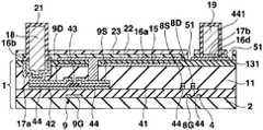
도 29∼도 34를 이용하여 제 5 실시형태에 있어서의 일렉트로루미네선트 디스플레이패널의 제조방법에 대하여 설명한다. 도 29∼도 34는 제조방법에 있어서의 각 공정의 단면도이고, 공정순서는 도 29∼도 34의 차례로 되어 있다. 또 도 29∼도 34에서는 제 2 실시형태에 있어서의 일렉트로루미네선트 디스플레이패널의 각 부에 대응하는 부분에 대하여 동일한 부호를 붙이고, 제 1 실시형태와 동일 공정에 대해서는 일부 생략한다.The manufacturing method of the electroluminescent display panel in 5th Embodiment is demonstrated using FIGS. 29-34. 29-34 is sectional drawing of each process in the manufacturing method, and the process order is in order of FIG. 29-34. 29-34, the same code | symbol is attached | subjected about the part corresponding to each part of the electroluminescent display panel in 2nd Embodiment, and abbreviate | omits about the process similar to 1st Embodiment.

우선 도 29에 나타내는 바와 같이, 트랜지스터어레이기판(1)을 제조한다. 다음으로 기상성장법 등의 성막공정, 포토리소그래피법 등의 마스크공정, 에칭 등의 형상가공공정을 이 차례로 실시함으로써 화소마다 반사금속막(15d)을 패터닝 형성한다.First, as shown in FIG. 29, thetransistor array substrate 1 is manufactured. Next, thereflective metal film 15d is patterned for each pixel by sequentially performing a film forming step such as a vapor phase growth method, a mask step such as a photolithography method, and a shape processing step such as etching.

다음으로 기상성장법을 실시함으로써 반사금속막(15d)을 피복하도록 투명절연막(131)을 전체 일면에 성막한다.Next, by performing the vapor phase growth method, the transparentinsulating film 131 is formed on one surface so as to cover thereflective metal film 15d.

다음으로 포토리소그래피법, 에칭법 등을 실시함으로써 각 전류제어트랜지스터(9)의 소스(9S)에 통하는 컨택트홀(12) 및 각 전류제어트랜지스터(9)의 드레인(9D)에 통하는 컨택트홀(13)을 평탄화막(11) 및 투명절연막(131)에 형성한다.Next, a photolithography method, an etching method, or the like is performed to contactholes 12 through thesource 9S of eachcurrent control transistor 9 and contact holes 13 through thedrain 9D of each current control transistor 9. ) Is formed in theplanarization film 11 and the transparentinsulating film 131.

또한 본 실시형태에서는 제 2 실시형태에 있어서의 유기EL분리절연막(14)을 형성하지 않는 것이 제 2 실시형태와 다르다.Note that the present embodiment differs from the second embodiment in that the organic ELisolation insulating film 14 in the second embodiment is not formed.

다음으로 도 30에 나타내는 바와 같이, 기상성장법에 의해서 투명금속산화물막(16)을 투명절연막(131)상의 일면에 성막한다. 투명금속산화물막(16)은 컨택트홀(12, 13) 내에 있어서도 표면에 성막되고, 전류제어트랜지스터(9)의 드레인(9D) 및 소스(9S)에 접한다.Next, as shown in FIG. 30, the transparentmetal oxide film 16 is formed into a film on the transparentinsulating film 131 by the vapor phase growth method. The transparentmetal oxide film 16 is formed on the surface of the contact holes 12 and 13 and is in contact with thedrain 9D and thesource 9S of thecurrent control transistor 9.

다음으로 스퍼터링 등의 기상성장법에 의해서 동, 니켈 등의 금속재료로 이루어지는 금속층(17)을 투명금속산화물막(16)상의 일면에 성막한다.Next, ametal layer 17 made of a metal material such as copper or nickel is formed on one surface on the transparentmetal oxide film 16 by a vapor phase growth method such as sputtering.

다음으로 도 31에 나타내는 바와 같이, 금속층(17)에 있어서의 컨택트홀(13)과 겹치고 또한 행방향을 따른 부분(17a) 및 반사금속막(15d)에 대하여 부분(17a)과 대향하는 변측에 행방향을 따른 EL라인(19)이 형성되는 부분(17b)이 노출되는 포토레지스트막(65)을 형성한다. 그리고 전해도금을 실시함으로써 노출된 밑바탕층부분(17a 17b)상에 트랜지스터(7, 8, 9)의 소스, 드레인, 게이트의 막두께보다도 두꺼운 막두께 2㎛∼100㎛, 5㎛∼50㎛폭의 동도금후막으로 이루어지는 전류원라인(18) 및 EL라인(19)을 형성한다. 이에 따라 행방향으로 배열된 복수의 화소의 전 류제어트랜지스터(9)의 드레인(9D)이 공통의 전류원라인(18)에 전기적으로 접속한 상태가 된다. 또한 전해도금 대신에 스퍼터링법 또는 승화증착법에 의해 동후막을 성막해도 좋다. 따라서 전류원라인(18, 18, ···) 및 EL라인(19, 19, ···)은 주사선(4)에 대하여 평행하게 설치되어 있다.Next, as shown in FIG. 31, the side part which overlaps with thecontact hole 13 in themetal layer 17, and faces thepart 17a with respect to thepart 17a and thereflective metal film 15d along a row direction is opposite. Thephotoresist film 65 in which theportion 17b in which the EL lines 19 are formed along the row direction is exposed is formed. On theunderlying layer portions 17a and 17b exposed by electroplating, the film thickness is 2 to 100 µm and 5 to 50 µm wider than the thickness of the source, drain, and gate of thetransistors 7, 8 and 9, respectively. Acurrent source line 18 and anEL line 19 made of a copper plated thick film are formed. As a result, thedrain 9D of thecurrent control transistors 9 of the plurality of pixels arranged in the row direction is electrically connected to the commoncurrent source line 18. Instead of electroplating, a copper thick film may be formed by sputtering or sublimation deposition. Therefore, the current source lines 18, 18, ..., and the EL lines 19, 19, ... are provided in parallel with thescan line 4.

다음으로 포토레지스트막(65)을 제거하고 나서 도 32에 나타내는 바와 같이, 전류원라인(18) 및 EL라인(19)을 마스크로 해서 노출된 밑바탕층(17)을 에칭 제거하고, 전류원라인(18, 18, ···)의 아래쪽에 밑바탕층(17a)을 잔존하며, EL라인(19, 19, ···)의 아래쪽에 밑바탕층(17b)을 잔존한다. 또한 투명금속산화물막(16)에 대하여 포토리소그래피법, 에칭법을 실시함으로써 화소전극(16a)을 패터닝하는 동시에, 전류원라인(18)을 마스크로 한 밑바탕층(17a)의 아래쪽에 설치된 투명금속산화물막(16)을 잔존시켜서 투명금속산화물밑바탕막(16b)을 형성하며, 밑바탕층(17b)의 아래쪽에 설치된 투명금속산화물막(16)을 잔존시켜서 보조전극라인(16d)을 형성한다. 보조전극라인(16d)은 EL라인(19)보다도 폭넓은 것이 바람직하다.Next, after removing thephotoresist film 65, as shown in FIG. 32, theunderlying layer 17 exposed using thecurrent source line 18 and theEL line 19 as a mask is etched away, and thecurrent source line 18 is removed. 18,... Remaining under thelayer 17a, and underneathEL line 19, 19, ... remain. In addition, the transparentmetal oxide film 16 is subjected to photolithography and etching to pattern thepixel electrode 16a, and the transparent metal oxide provided below theunderlying layer 17a using thecurrent source line 18 as a mask. Thefilm 16 is left to form a transparentmetal oxide underlayer 16b, and the transparentmetal oxide film 16 provided below theunderlayer 17b is left to form anauxiliary electrode line 16d. Theauxiliary electrode line 16d is preferably wider than theEL line 19.

다음으로 도 33에 나타내는 바와 같이, 전류원라인(18)을 피복하도록 전류원라인절연막(21)을 형성하는 동시에, EL라인(19)을 피복하도록 EL라인절연막(441)을 전류원라인절연막(21)과 동일 공정에서 형성한다. 이상에 의해 유기EL구동기판이 완성된다.Next, as shown in FIG. 33, the current sourceline insulating film 21 is formed so as to cover thecurrent source line 18, and the ELline insulating film 441 is covered with the current sourceline insulating film 21 so as to cover theEL line 19. Next, as shown in FIG. It is formed in the same process. The organic EL driving substrate is completed by the above.

다음으로 PEDOT(폴리티오펜) 및 도펀트인 PSS(폴리스티렌술폰산)으로 이루어지는 정공수송층(22)을 액적토출법(잉크젯법), 스핀코트법, 딥코트법, 니들에 의한 적하법 등의 습식성막법에 의해서 성막한다. 정공수송층(22)은 트랜지스터어레이기판(1)의 일면에 성막하여 모든 화소에 공통시켜도 좋고, 화소마다 독립하도록 형성해도 좋다.Next, the wet-transporting method of thehole transport layer 22 made of PEDOT (polythiophene) and dopant PSS (polystyrene sulfonic acid) is a liquid film deposition method such as a droplet ejection method (ink jet method), spin coating method, dip coating method, dropping method by needle, etc. Formation by Thehole transport layer 22 may be formed on one surface of thetransistor array substrate 1 to be common to all the pixels, or may be formed so as to be independent for each pixel.

정공수송층(22)의 건조 후, 제 1 실시형태와 마찬가지로 폴리플루오렌계 발광재료로 이루어지는 발광층(23)을 액적토출법(잉크젯방법), 니들에 의한 적하법, 인쇄법 등의 습식성막법에 의해서 화소마다 패터닝한다. 여기에서 정공수송층(22)의 막두께나 발광층(23)의 막두께는 EL라인(19)의 막두께보다도 얇다. 그리고 정공수송층(22)이 되는 용액 또는 현탁액의 높이 및 화소영역에 피복했을 때의 발광층(23)을 포함하는 용액 또는 현탁액의 높이는 전류원라인(18)의 높이나 EL라인(19)의 높이보다도 낮다. 따라서 정공수송층(22)이 되는 용액 또는 현탁액 및 발광층(23)이 되는 용액 또는 현탁액은 전류원라인(18) 및 EL라인(19)을 넘어서 이웃한 행의 화소에 유출하는 일은 없다. 이와 같이 전류원라인(18) 및 EL라인(19)은 정공수송층(22)이 되는 용액 또는 현탁액 및 발광층(23)이 되는 용액 또는 현탁액의 유출을 방지하는 격벽으로서 기능한다. 따라서 전류원라인(18) 및 EL라인(19)을 따라서 둘러싸여진 행방향의 복수의 화소는 동일색으로 발광하는 발광층으로 하면 전류원라인(18) 및 EL라인(19)간에 일괄하여 발광층(23)을 포함하는 용액 또는 현탁액을 유입시킴으로써 행방향의 복수의 화소에 발광층(23)을 일괄하여 성막할 수 있다.After drying thehole transport layer 22, thelight emitting layer 23 made of a polyfluorene-based light emitting material is subjected to a wet film formation method such as a droplet ejection method (ink jet method), a dropping method using a needle, a printing method or the like in the first embodiment. Patterning is performed for each pixel. Here, the film thickness of thehole transport layer 22 and the film thickness of thelight emitting layer 23 are thinner than the film thickness of theEL line 19. The height of the solution or suspension which becomes thehole transport layer 22 and the height of the solution or suspension including thelight emitting layer 23 when the pixel region is coated is lower than the height of thecurrent source line 18 or the height of theEL line 19. Therefore, the solution or suspension serving as thehole transport layer 22 and the solution or suspension serving as thelight emitting layer 23 do not flow over thecurrent source line 18 and theEL line 19 to the pixels in the adjacent rows. In this way, thecurrent source line 18 and theEL line 19 function as partition walls for preventing the outflow of the solution or suspension serving as thehole transport layer 22 and the solution or suspension serving as thelight emitting layer 23. Therefore, when the plurality of pixels in the row direction surrounded by thecurrent source line 18 and theEL line 19 are light emitting layers emitting light of the same color, thelight emitting layer 23 is collectively arranged between thecurrent source line 18 and theEL line 19. Thelight emitting layer 23 can be formed into a film collectively in the several pixel of a row direction by flowing in the solution or suspension containing.

발광층(23)의 건조 후, 보조전극라인(16d)의 일부표면이 노출하도록 정공수송층(22) 및 발광층(23)에 컨택트홀(51)을 형성한다.After thelight emitting layer 23 is dried, contact holes 51 are formed in thehole transport layer 22 and thelight emitting layer 23 so that a part of the surface of theauxiliary electrode line 16d is exposed.

다음으로 도 34에 나타내는 바와 같이, 증착 등의 기상성장법에 의해서 마그네슘, 칼슘, 리튬, 바륨, 희토류금속 등의 낮은 일함수의 재료로 이루어지는 전자주입층과, 산화인듐, 산화아염 혹은 산화주석 또는 이들 중의 적어도 하나를 포함하는 혼합물(예를 들면, 주석도프산화인듐(ITO), 아연도프산화인듐, 카드뮴-주석산화물(CTO))을 갖는 투명도전층과의 이층구조의 공통전극(24)을 캐소드전극으로서 일면에 성막한다. 전자주입층은 10nm∼200nm의 두께로 가시광이 투과할 정도로 얇기 때문에 전류원라인(18)이나 EL라인(19)의 단차에 의해서 절단되어도 좋은데, 공통전극(24)의 투명도전층은 복수의 화소의 유기EL소자(26)의 한쪽의 전극을 서로 등전위로 하기 위해 전류원라인(18)표면의 전류원라인절연막(21)상에 넘고 또한 EL라인(19)표면의 EL라인절연막(441)상에 걸치도록 성막되어 있다. 공통전극(24)은 컨택트홀(51)을 통하여 보조전극라인(16d) 및 EL라인(19)에 접속되어 있다. 이와 같이 발광층(23)은 공통전극(24)에 밀착한 상태에서 공통전극(24)에 의해서 피복되고, 또한 EL라인(19)도 공통전극(24)에 밀착한 상태에서 공통전극(24)에 의해서 피복되어 유기EL소자(26)가 형성된다.Next, as shown in FIG. 34, the electron injection layer which consists of materials of low work function, such as magnesium, calcium, lithium, barium, and rare earth metals by vapor phase growth methods, such as vapor deposition, indium oxide, chlorine oxide, or tin oxide, Cathode acommon electrode 24 of a two-layer structure with a transparent conductive layer having a mixture containing at least one of them (e.g., indium tin dope oxide (ITO), indium zinc dope oxide, cadmium-tin oxide (CTO)). It is formed on one surface as an electrode. Since the electron injection layer is thin enough to transmit visible light with a thickness of 10 nm to 200 nm, the electron injection layer may be cut by the step of thecurrent source line 18 or theEL line 19. The transparent conductive layer of thecommon electrode 24 is formed of organic materials of a plurality of pixels. Films are formed so as to pass on the current sourceline insulating film 21 on the surface of thecurrent source line 18 and across the ELline insulating film 441 on the surface of theEL line 19 so that one electrode of theEL element 26 is equipotential to each other. It is. Thecommon electrode 24 is connected to theauxiliary electrode line 16d and theEL line 19 through thecontact hole 51. In this way, thelight emitting layer 23 is covered by thecommon electrode 24 in a state of being in close contact with thecommon electrode 24, and theEL line 19 is also in contact with thecommon electrode 24. Theorganic EL element 26 is formed by covering the same.

다음으로 스핀코트법, 딥코트법, 기상성장법에 의해서 오버코트절연층(25)을 일면에 성막하고, 주사드라이버(32), 데이터드라이버(33) 및 전류원드라이버(34)를 접속하고 나서 투명밀봉기판을 맞붙인다.Next, theovercoat insulating layer 25 is formed on one surface by the spin coating method, the dip coating method, and the vapor phase growth method, and thescan driver 32, thedata driver 33, and thecurrent source driver 34 are connected, and then transparently sealed. Glue the substrate.

이상에 의해 액티브매트릭스 구동방식의 표시장치가 완성된다.This completes the display of the active matrix drive system.

제 5 실시형태에 있어서도 전류원라인(18) 및 EL라인(19)을 트랜지스터(7, 8, 9)의 일부를 구성하는 도전막과는 다른 막으로 형성되어 있기 때문에 전류원라 인(18) 및 EL라인(19)을 트랜지스터(7, 8, 9)의 드레인, 소스, 게이트나 신호전류선(3), 주사선(4) 등보다도 후막으로 할 수 있다.Also in the fifth embodiment, since thecurrent source line 18 and theEL line 19 are formed of a different film from the conductive film forming part of thetransistors 7, 8 and 9, the current source lines 18 and theEL line 19 are formed. Theline 19 can be thicker than the drain, the source, the gate, the signalcurrent line 3, thescan line 4, or the like of thetransistors 7, 8, 9.

<제 6 실시형태>Sixth Embodiment

제 1 실시형태에서는 전류원라인(18) 및 EL라인(19)을 트랜지스터층(기판(2)의 표면으로부터 평탄화막(11)의 표면까지의 사이의 다층막)의 위에 형성했는데, 본 실시형태에서는 트랜지스터층의 아래에 전류원라인(18) 및 EL라인(19)을 형성하고 있다. 구체적으로는 도 35∼도 40에 나타내는 제조방법으로 되어 있다.In the first embodiment, thecurrent source line 18 and theEL line 19 are formed on the transistor layer (multilayer film between the surface of thesubstrate 2 and the surface of the planarization film 11). In this embodiment, the transistor Acurrent source line 18 and anEL line 19 are formed under the layer. Specifically, it is a manufacturing method shown in FIGS. 35-40.

도 35∼도 41을 이용하여 제 6 실시형태에 있어서의 일렉트로루미네선트 디스플레이패널의 제조방법에 대하여 설명한다. 도 35∼도 40은 제조방법에 있어서의 각 공정의 단면도이고, 공정순서는 도 35∼도 40의 차례로 되어 있다. 또한 도 35∼도 40에서는 제 1 실시형태에 있어서의 일렉트로루미네선트 디스플레이패널의 각 부에 대응하는 부분에 대하여 동일한 부호를 붙이고, 제 1 실시형태와 동일 공정 부분에 대해서는 일부 생략한다.The manufacturing method of the electroluminescent display panel in 6th Embodiment is demonstrated using FIGS. 35-41. 35-40 is sectional drawing of each process in a manufacturing method, and the process order is in order of FIG. 35-40. 35-40, the same code | symbol is attached | subjected about the part corresponding to each part of the electroluminescent display panel in 1st Embodiment, and it abbreviate | omits a part about the same process part as 1st Embodiment.

우선 도 35에 나타내는 바와 같이, 전해도금을 실시함으로써 5㎛∼50㎛폭으로 또한 2㎛∼100㎛의 막두께인 복수의 전류원라인(18) 및 복수의 EL라인(19)을 기판(2)상에 패터닝한다. 전류원라인(18) 및 EL라인(19)을 패터닝함에 있어서 전류원라인(18)을 EL라인(19)에 대하여 평행하게 설치하고, 전류원라인(18) 및 EL라인(19)을 기판(2)의 테두리까지 연장하도록 또는 전류원라인(18) 및 EL라인(19)이 기판(2)의 가로방향으로 연장하도록 전류원라인(18) 및 EL라인(19)을 패터닝한다. 전류원라인(18) 및 EL라인(19)은 후술하는 트랜지스터(7, 8, 9)의 소스, 드레인, 게이트보다 두껍게 퇴적되어 있기 때문에 이들 전극보다도 단위배선의 길이당의 저항이 낮게 설정되어 있다.First, as shown in FIG. 35, electroplating is carried out to provide a plurality of current source lines 18 and a plurality ofEL lines 19 having a thickness of 5 to 50 µm and a thickness of 2 to 100 µm. Pattern on phase. In patterning thecurrent source line 18 and theEL line 19, thecurrent source line 18 is provided in parallel to theEL line 19, and thecurrent source line 18 and theEL line 19 are formed on thesubstrate 2. Thecurrent source line 18 and theEL line 19 are patterned so as to extend to the edge or thecurrent source line 18 and theEL line 19 extend in the transverse direction of thesubstrate 2. Since thecurrent source line 18 and theEL line 19 are deposited thicker than the sources, drains, and gates of thetransistors 7, 8, and 9 described later, the resistance per unit wiring length is set lower than those of these electrodes.

다음으로 층간절연막(501)을 기판(2)상에 전체 일면에 성막하고, 전류원라인(18) 및 EL라인(19)을 층간절연막(501)으로 피복한다. 다음으로 하나의 화소당 전류원라인(18)까지 통하는 컨택트홀(502)과, EL라인(19)까지 통하는 컨택트홀(503)을 층간절연막(501)에 형성한다.Next, theinterlayer insulating film 501 is formed on the entire surface of thesubstrate 2, and thecurrent source line 18 and theEL line 19 are covered with theinterlayer insulating film 501. Next, acontact hole 502 through up to onecurrent source line 18 per pixel and acontact hole 503 through up to anEL line 19 are formed in theinterlayer insulating film 501.

다음으로 도 36에 나타내는 바와 같이, 기상성장법과 같은 성막공정, 포토리소그래피법과 같은 마스크공정, 에칭과 같은 형상가공공정을 적절히 실시함으로써 하나의 화소당 세개의 트랜지스터(7, 8, 9)를 패터닝 형성한다. 여기에서 트랜지스터(7, 8, 9)의 게이트의 기초가 되는 도전성박막이 컨택트홀(502)에 매설하도록 패터닝된 게이트밑바탕막(511a)이 형성되고, 컨택트홀(503)에 매설하도록 패터닝된 게이트밑바탕막(511b)이 형성된다. 또 게이트밑바탕막(511a)이 노출하는 컨택트홀 및 게이트밑바탕막(511a)이 노출하는 컨택트홀을 게이트절연막(41)에 일괄하여 설치하고, 트랜지스터(7, 8, 9)의 소스, 드레인의 기초가 되는 도전성박막을 패터닝하여 각각에 전류제어트랜지스터(9)의 드레인(9D) 및 소스, 드레인밑바탕막(504)이 매설된다. 트랜지스터(7, 8, 9)의 게이트의 기초가 되는 도전성박막은 일부가 신호전류선(3)으로서 패터닝 형성된다.Next, as shown in FIG. 36, threetransistors 7, 8, and 9 are patterned for each pixel by appropriately performing a film forming process such as a vapor phase growth method, a mask process such as a photolithography method, and a shape processing process such as etching. do. Here, thegate underlayer 511a is formed so that the conductive thin film serving as the base of the gates of thetransistors 7, 8, and 9 is embedded in thecontact hole 502, and the gate patterned so as to be embedded in thecontact hole 503. Anunderlayer 511b is formed. In addition, the contact holes exposed by thegate underlayer 511a and the contact holes exposed by thegate underlayer 511a are collectively provided in thegate insulating layer 41, and the bases of the sources and drains of thetransistors 7, 8, and 9 are provided. The conductive thin film to be used is patterned, and thedrain 9D, the source, and theunderlying drain film 504 of thecurrent control transistor 9 are embedded in each. The conductive thin film serving as the basis of the gates of thetransistors 7, 8, 9 is partially patterned as the signalcurrent line 3.

다음으로 평탄화막(11)에 대하여 포토리소그래피법, 에칭법 등을 실시함으로써 각 전류제어트랜지스터(9)의 소스(9S)에 통하는 컨택트홀(12) 및 밑바탕막(504)에 통하는 컨택트홀(505)을 평탄화막(11)으로 형성한다.Next, theplanarization film 11 is subjected to photolithography, etching, or the like, so that thecontact hole 12 through thesource 9S of eachcurrent control transistor 9 and thecontact hole 505 through theunderlying film 504 are formed. ) Is formed into theplanarization film 11.

다음으로 도 37에 나타내는 바와 같이, 기상성장법 등의 성막공정, 포토리소그래피법 등의 마스크공정, 에칭 등의 형상가공공정을 이 차례로 실시함으로써 화소마다 반사금속막(15d)을 패터닝 형성한다. 다음으로 기상성장법을 실시함으로써 반사금속막(15d)을 피복하도록 투명절연막(131)을 전체 일면에 성막한다.Next, as shown in FIG. 37, thereflective metal film 15d is patterned for each pixel by performing a film forming process such as a vapor phase growth method, a mask process such as a photolithography method, and a shape processing process such as etching in this order. Next, by performing the vapor phase growth method, the transparentinsulating film 131 is formed on one surface so as to cover thereflective metal film 15d.

다음으로 투명절연막(131)에도 컨택트홀(12) 및 컨택트홀(505)에 맞추어서 컨택트홀을 형성한다.Next, a contact hole is formed in the transparentinsulating film 131 in accordance with thecontact hole 12 and thecontact hole 505.

다음으로 기상성장법에 의해서 투명금속산화물막을 투명절연막(131)상의 일면에 성막한다. 투명금속산화물막은 컨택트홀(12, 505) 내에 있어서도 표면에 성막되고, 전류제어트랜지스터(9)의 소스(9S) 및 밑바탕막(504)에 접한다.Next, a transparent metal oxide film is formed on one surface on the transparentinsulating film 131 by the vapor phase growth method. The transparent metal oxide film is also formed on the surface of the contact holes 12 and 505 and is in contact with thesource 9S and theunderlying film 504 of thecurrent control transistor 9.

다음으로 도 38에 나타내는 바와 같이, 투명금속산화물막에 대하여 포토리소그래피법, 에칭법을 실시함으로써 컨택트홀(12)을 통하여 전류제어트랜지스터(9)의 소스(9S)와 접속되는 화소전극(16a)을 형성하는 동시에, 컨택트홀(505)을 통하여 보조전극라인(16e)을 형성한다. 또한 도 38은 도 41의 (ⅩⅩⅩⅤⅠⅠⅠ)-(ⅩⅩⅩⅤⅠⅠⅠ)선을 따라서 두께방향으로 절단했을 때의 대략 단면도이다.38, thepixel electrode 16a connected to thesource 9S of thecurrent control transistor 9 through thecontact hole 12 by performing photolithography and etching on the transparent metal oxide film. At the same time, theauxiliary electrode line 16e is formed through thecontact hole 505. 38 is a cross sectional view taken along the line (XVI)-(XVI) in FIG. 41 in the thickness direction.

다음으로 도 39에 나타내는 바와 같이, 포토리소그래피법에 의해서 폴리이미드 등의 감광성수지로 이루어지는 메시상의 격벽(506)을 패터닝한다. 여기에서 화소전극(16a)이 격벽(506)에 의한 메시의 사이에 위요되도록 격벽(506)을 패터닝한다.Next, as shown in FIG. 39, the mesh-shapedpartition wall 506 which consists of photosensitive resins, such as a polyimide, is patterned by the photolithographic method. Here, thepartition wall 506 is patterned so that thepixel electrode 16a is positioned between the meshes by thepartition wall 506.

다음으로 PEDOT(폴리티오펜) 및 도펀트인 PSS(폴리스티렌술폰산)으로 이루어지는 정공수송층(22)을 액적토출법(잉크젯법), 스핀코트법, 딥코트법, 니들에 의한 적하법 등의 습식성막법에 의해서 성막한다. 정공수송층(22)은 트랜지스터어레이기판(1)의 일면에 형성하여 모든 화소에 공통시켜도 좋고, 화소마다 독립하도록 형성해도 좋다.Next, the wet-transporting method of thehole transport layer 22 made of PEDOT (polythiophene) and dopant PSS (polystyrene sulfonic acid) is a liquid film deposition method such as a droplet ejection method (ink jet method), spin coating method, dip coating method, dropping method by needle, etc. Formation by Thehole transport layer 22 may be formed on one surface of thetransistor array substrate 1 to be common to all the pixels, or may be formed so as to be independent for each pixel.

정공수송층(22)의 건조 후, 제 1 실시형태와 마찬가지로 습식성막법에 의해서 화소마다 패터닝한다. 여기에서 정공수송층(22)의 막두께나 발광층(23)의 막두께는 격벽(231)의 막두께보다도 얇다. 그리고 정공수송층(22)이 되는 용액 또는 현탁액의 높이 및 화소영역에 피복했을 때의 발광층(23)이 되는 용액 또는 현탁액의 높이는 격벽(506)의 높이보다도 낮다. 따라서 정공수송층(22)이 되는 용액 또는 현탁액 및 발광층(23)이 되는 용액 또는 현탁액은 격벽(506)을 넘어서 이웃한 행의 화소에 유출하는 일은 없다. 이와 같이 격벽(506)은 정공수송층(22)이 되는 용액 또는 현택액 및 발광층(23)이 되는 용액 또는 현탁액의 유출을 방지하는 격벽으로서 기능한다. 따라서 격벽(506)을 따라서 둘러싸여진 행방향의 복수의 화소는 동일색으로 발광하는 발광층으로 하면 격벽(506)간에 일괄하여 발광층(23)을 포함하는 용액 또는 현탁액을 유입시킴으로써 행방향의 복수의 화소에 발광층(23)을 일괄하여 성막할 수 있다.After thehole transport layer 22 is dried, patterning is performed for each pixel by the wet film forming method as in the first embodiment. Here, the film thickness of thehole transport layer 22 and the film thickness of thelight emitting layer 23 are thinner than the film thickness of thepartition wall 231. The height of the solution or suspension serving as thehole transport layer 22 and the height of the solution or suspension serving as thelight emitting layer 23 when the pixel region is coated are lower than the height of thepartition wall 506. Therefore, the solution or suspension serving as thehole transport layer 22 and the solution or suspension serving as thelight emitting layer 23 do not flow over thepartition 506 to the pixels in the adjacent rows. Thus, thepartition 506 functions as a partition which prevents the outflow of the solution or suspension which becomes thehole transport layer 22, and the solution or suspension which becomes thelight emitting layer 23. As shown in FIG. Therefore, when the plurality of pixels in the row direction surrounded by thepartition wall 506 are the light emitting layers emitting light of the same color, the plurality of pixels in the row direction are introduced by introducing a solution or a suspension including thelight emitting layer 23 collectively between thepartition walls 506. Thelight emitting layer 23 can be collectively formed into a film.

발광층(23)의 건조 후, 보조전극라인(16e)의 일부표면이 노출하도록 정공수송층(22) 및 발광층(23)에 컨택트홀(51)을 형성한다.After thelight emitting layer 23 is dried, contact holes 51 are formed in thehole transport layer 22 and thelight emitting layer 23 so that a part of the surface of theauxiliary electrode line 16e is exposed.

다음으로 도 40에 나타내는 바와 같이, 증착 등의 기상성장법에 의해서 마그네슘, 칼슘, 리튬, 바륨, 희토류금속 등의 낮은 일함수의 재료로 이루어지는 전자주입층과, 산화인듐, 산화아연 혹은 산화주석 또는 이들 중의 적어도 하나를 포함 하는 혼합물(예를 들면, 주석도프산화인듐(ITO), 아연도프산화인듐, 카드뮴-주석산화물(CTO))을 갖는 투명도전층과의 이층구조의 공통전극(24)을 캐소드전극으로서 일면에 성막한다. 전자주입층은 10nm∼200nm의 두께로 가시광이 투과할 정도로 얇기 때문에 격벽(506)의 단차에 의해서 절단되어도 좋은데, 공통전극(24)의 투명도전층은 복수의 화소의 유기EL소자(26)의 한쪽의 전극을 서로 등전위로 하기 위해 격벽(506)표면의 전류원라인절연막(21)상에 넘고 또한 격벽(506)표면의 EL라인절연막(441)상에 걸치도록 성막되어 있다. 공통전극(24)는 컨택트홀(51)을 통하여 보조전극라인(16e)에 접속되어 있다. 이와 같이 발광층(23)은 공통전극(24)에 밀착한 상태로 공통전극(24)에 의해서 피복되고, 또한 격벽(506)도 공통전극(24)에 밀착한 상태로 공통전극(24)에 의해서 피복되어 유기EL소자(26)가 형성된다.Next, as shown in FIG. 40, the electron injection layer which consists of materials of low work function, such as magnesium, calcium, lithium, barium, and rare earth metals by vapor phase growth methods, such as vapor deposition, indium oxide, zinc oxide, or tin oxide, or Cathode acommon electrode 24 of a two-layer structure with a transparent conductive layer having a mixture containing at least one of them (e.g., indium tin dope oxide (ITO), indium zinc dope oxide, cadmium-tin oxide (CTO)). It is formed on one surface as an electrode. Since the electron injection layer has a thickness of 10 nm to 200 nm and is thin enough to transmit visible light, the electron injection layer may be cut by a step of thepartition wall 506. The transparent conductive layer of thecommon electrode 24 has one side of theorganic EL element 26 of the plurality of pixels. The electrodes are formed so as to pass over the current sourceline insulating film 21 on the surface of thebarrier rib 506 and over the ELline insulating film 441 on the surface of thebarrier rib 506 so as to equipotentially. Thecommon electrode 24 is connected to theauxiliary electrode line 16e through thecontact hole 51. In this manner, thelight emitting layer 23 is covered by thecommon electrode 24 while being in close contact with thecommon electrode 24, and thepartition wall 506 is also in contact with thecommon electrode 24 by thecommon electrode 24. Theorganic EL element 26 is formed by covering.

다음으로 도 40에 나타내는 바와 같이, 스핀코트법, 딥코트법, 기상성장법에 의해서 오버코트절연층(25)을 일면에 성막하고, 주사드라이버(32), 데이터드라이버(33) 및 전류원드라이버(34)를 접속하고 나서 투명밀봉기판을 맞붙인다.Next, as shown in FIG. 40, theovercoat insulating layer 25 is formed on one surface by the spin coating method, the dip coating method, and the vapor phase growth method, and thescan driver 32, thedata driver 33, and thecurrent source driver 34 are formed. ), And then attach the transparent sealing substrate.

이상에 의해 액티브매트릭스 구동방식의 표시장치가 완성된다.This completes the display of the active matrix drive system.

제 6 실시형태에 있어서도 전류원라인(18) 및 EL라인(19)를 트랜지스터(7, 8, 9)와는 별도의 공정에서 트랜지스터(7, 8, 9)의 소스, 드레인, 게이트와는 다른 도전막을 패터닝하여 이루어지기 때문에 전류원라인(18) 및 EL라인(19)을 트랜지스터(7, 8, 9)의 드레인, 소스, 게이트나 신호전류선(3), 주사선(4) 등보다도 후막으로 할 수 있고, 전류원라인(18)이나 EL라인(19)의 전기저항을 낮게 할 수 있다. 그 때문에 전류원라인(18)이나 EL라인(19)에 있어서의 신호지연이나 전압강하를 억 제하거나 할 수 있다.Also in the sixth embodiment, thecurrent source line 18 and theEL line 19 are separated from thetransistors 7, 8, and 9 in a process separate from the source, drain, and gate of thetransistors 7, 8, and 9. By patterning, thecurrent source line 18 and theEL line 19 can be thicker than the drains, sources, gates, signalcurrent lines 3,scan lines 4, etc. of thetransistors 7, 8, 9, and the like. The electrical resistance of thecurrent source line 18 and theEL line 19 can be lowered. Therefore, the signal delay and the voltage drop in thecurrent source line 18 and theEL line 19 can be suppressed.

<제 7 실시형태>Seventh Embodiment

도 42∼도 43을 이용하여 제 7 실시형태에 있어서의 일렉트로루미네선트 디스플레이패널의 제조방법에 대해서 설명한다. 도 42∼도 43은 제조방법에 있어서의 각 공정의 단면도이고, 공정순서는 도 42∼도 43의 차례로 되어 있다. 또한 도 42∼도 43에서는 제 6 실시형태에 있어서의 일렉트로루미네선트 디스플레이패널의 각 부에 대응하는 부분에 대하여 동일한 부호를 붙인다. 또 제 7 실시형태에 있어서는 화소전극이 형성되는 공정까지는 제 6 실시형태의 도 35∼도 38과 동일 공정이므로, 그 설명을 생략한다.The manufacturing method of the electroluminescent display panel in 7th Embodiment is demonstrated using FIGS. 42-43. 42-43 is sectional drawing of each process in the manufacturing method, and the process order is in order of FIG. 42-43. 42 to 43, the same reference numerals are attached to the parts corresponding to the parts of the electroluminescent display panel in the sixth embodiment. In the seventh embodiment, the steps up to the step of forming the pixel electrodes are the same as those in Figs. 35 to 38 in the sixth embodiment, and thus description thereof is omitted.

화소전극(16a)을 형성한 후, 도 42에 나타내는 바와 같이, 포토리소그래피법에 의해서 전류원라인(18)을 따라서 격벽(507)을 패터닝하는 동시에, 격벽(507)의 형성과 동일한 공정에서 EL라인(19)을 따라 격벽(508, 509)을 형성한다. 여기에서 화소전극(16a)이 격벽(507)과 격벽(508)의 사이에 위치하도록 격벽(507,508)이 형성되고, 또한 밑바탕막(504)의 위에 잔류한 보조전극라인(16e)이 평면에서 보아 격벽(508)과 격벽(509)의 사이에 위치하도록 격벽(508) 및 격벽(509)이 형성되어 있다.After forming thepixel electrode 16a, as shown in FIG. 42, thepartition wall 507 is patterned along thecurrent source line 18 by the photolithography method, and the EL line is formed in the same process as the formation of thepartition wall 507. FIG.Partition walls 508 and 509 are formed along 19. Here,barrier ribs 507 and 508 are formed such that thepixel electrode 16a is positioned between thebarrier rib 507 and thebarrier rib 508, and theauxiliary electrode line 16e remaining on thebase film 504 is viewed in plan view. Thepartition 508 and thepartition 509 are formed so as to be located between thepartition 508 and thepartition 509.

다음으로 격벽(508)과 격벽(509)의 사이에 도전성페이스트(510)를 매립한다. 이에 따라, 밑바탕막(504)의 위에 잔류한 보조전극라인(16e)에 대하여 도전성페이스트(510)가 밀착한다.Next, theconductive paste 510 is buried between thepartition wall 508 and thepartition wall 509. Accordingly, theconductive paste 510 is in close contact with theauxiliary electrode line 16e remaining on theunderlayer 504.

도전성페이스트(510)의 건조 후, 제 6 실시형태와 마찬가지로 정공수송층 (22), 발광층(23)을 성막한다. 이 때, 격벽(507) 및 격벽(508)은 제 6 실시형태의 격벽(506)과 같은 기능을 갖는다.After drying theconductive paste 510, thehole transport layer 22 and thelight emitting layer 23 are formed as in the sixth embodiment. At this time, thepartition 507 and thepartition 508 have the same function as thepartition 506 of 6th Embodiment.

다음으로 도 43에 나타내는 바와 같이, 제 6 실시형태와 마찬가지로 공통전극(24)을 일면에 성막한다. 이에 따라, 발광층(23)은 공통전극(24)에 밀착된 상태에서 공통전극(24)에 의해서 피복된다. 또한, 도전성페이스트(510)도 공통전극(24)에 밀착한다. 따라서, 공통전극(24)은 도전성페이스트(510), 보조전극라인(16e), 소스, 드레인밑바탕막(504), 게이트밑바탕막(511b)을 통하여 EL라인(19)에 접속된다.Next, as shown in FIG. 43, thecommon electrode 24 is formed into one film similarly to 6th Embodiment. Accordingly, thelight emitting layer 23 is covered by thecommon electrode 24 in a state of being in close contact with thecommon electrode 24. In addition, theconductive paste 510 is in close contact with thecommon electrode 24. Therefore, thecommon electrode 24 is connected to theEL line 19 through theconductive paste 510, theauxiliary electrode line 16e, the source and the drainunderlying film 504, and thegate underlying film 511b.

다음으로 스핀코트법, 딥코트법, 기상성장법에 의해서 오버코트절연층(25)을일면에 성막하고, 주사드라이버(32), 데이터드라이버(33) 및 전류원드라이버(34)를 접속하고 나서 투명밀봉기판을 맞붙인다.Next, theovercoat insulating layer 25 is formed on one surface by the spin coating method, the dip coating method, and the vapor phase growth method, and thescan driver 32, thedata driver 33, and thecurrent source driver 34 are connected, and then transparently sealed. Glue the substrate.

이상에 의해, 액티브매트릭스 구동방식의 표시장치가 완성된다.By the above, the display device of the active matrix drive system is completed.

제 7 실시형태에 있어서도, 전류원라인(18) 및 EL라인(19)을 트랜지스터(7, 8, 9)와는 별도의 공정에서 패터닝했기 때문에, 전류원라인(18) 및 EL라인(19)을 트랜지스터(7, 8, 9)의 드레인, 소스, 게이트나 신호전류원(3), 주사선(4) 등보다도 후막으로 해서 트랜지스터(7, 8, 9)보다도 상대적으로 저저항으로 할 수 있어, 전류원라인(18)이나 EL라인(19)의 전기저항을 낮게 할 수 있다. 그 때문에 전류원라인(18)이나 EL라인(19)에 있어서의 신호지연이나 전압강하를 억제하거나 할 수 있다.Also in the seventh embodiment, since thecurrent source line 18 and theEL line 19 are patterned in a process separate from thetransistors 7, 8 and 9, thecurrent source line 18 and theEL line 19 are connected to the transistor ( As a thicker film than the drains, sources, gates, signalcurrent sources 3,scan lines 4, etc. of the 7, 8, and 9, the resistance can be made relatively lower than thetransistors 7, 8, and 9, and the current source lines 18 ) AndEL line 19 can be made low. Therefore, the signal delay and the voltage drop in thecurrent source line 18 and theEL line 19 can be suppressed.

상기 각 실시형태에서는 반사금속막(15)을 설치해서 공통전극(24)측으로부터 발광층(23)의 발광을 출사시켰지만, 이것에 한정하지 않고, 반사금속막(15)을 설치하지 않고, 화소전극(16)측으로부터 발광층(23)의 발광을 출사시켜도 좋다. 이 경우, 공통전극(24)은 불투명 또는 광반사성인 것이 바람직하고, 특히 낮은 일함수의 전자방출막과, 전자방출막을 피복하여 보호하는 높은 일함수의 도전막과의 복수층 구조인 것이 바람직하다.In each of the above embodiments, although thereflective metal film 15 is provided to emit light from thelight emitting layer 23 from thecommon electrode 24 side, the pixel electrode is not limited to this and thereflective metal film 15 is not provided. The light emission of thelight emitting layer 23 may be emitted from the (16) side. In this case, thecommon electrode 24 is preferably opaque or light reflective, and particularly preferably a multilayer structure of a low work function electron emission film and a high work function conductive film covering and protecting the electron emission film. .

<제 8 실시형태>Eighth Embodiment

도 44∼도 50을 이용하여 발광소자인 유기일렉트로루미네선트소자를 화소로 하는 표시장치의 제조방법에 대해서 설명한다. 도 44∼도 50은 제조방법에 있어서의 각 공정의 단면도이고, 공정순서는 도 44∼도 50의 차례로 되어 있다. 제 1 실시형태에 있어서의 일렉트로루미네선트 디스플레이패널의 각 부에 대응하는 부분에 대하여 동일한 부호를 붙이고, 제 1 실시형태와 동일한 공정 부분에 대해서는 일부 생략한다.A manufacturing method of a display device using an organic electroluminescent element as a light emitting element as a pixel will be described with reference to FIGS. 44 to 50. 44-50 is sectional drawing of each process in the manufacturing method, and the process order is in order of FIGS. 44-50. The same code | symbol is attached | subjected about the part corresponding to each part of the electroluminescent display panel in 1st Embodiment, and it abbreviate | omits a part about the process part similar to 1st Embodiment.

또한 도 44∼도 50은 전류제어트랜지스터(9)를 주사선(4)에 직교하는 면을 따라 절단한 경우의 단면도이며, 하나의 화소를 나타낸다. 다른 화소도 각 공정에서는 도 44∼도 50의 상태로 되어 있다.44 to 50 are cross-sectional views when thecurrent control transistor 9 is cut along a plane orthogonal to thescan line 4, and shows one pixel. The other pixels are also in the state of Figs. 44 to 50 at each step.

도 44에 나타내는 바와 같이, 준비한 트랜지스터어레이기판(1)에 대해 포토리소그래피법, 에칭법 등을 실시함으로써, 각 전류제어트랜지스터(9)의 소스(9S)에 통하는 컨택트홀(12) 및 각 전류제어트랜지스터(9)의 드레인(9D)에 통하는 컨택트홀(13)을 절연막(11)에 형성한다.As shown in FIG. 44, the photolithography method, the etching method, etc. are performed with respect to the prepared transistor array board |substrate 1, and thecontact hole 12 and each current control which communicate with thesource 9S of eachcurrent control transistor 9 are controlled. Acontact hole 13 through thedrain 9D of thetransistor 9 is formed in the insulatingfilm 11.

다음으로 스퍼터링이나 증착과 같은 기상성장법에 의해서 알루미늄, 티탄, 금 등의 금속단체 혹은 합금 또는 투명금속산화물막 등에서 선택된 도전재료로 이루어지는 도전막을 트랜지스터어레이기판(1)상의 일면에 성막한다. 이 도전막은 컨택트홀(12, 13) 내에 있어서도 표면에 성막된다. 계속해서, 도전막상에 산화인듐, 산화아연 혹은 산화주석 또는 이들 중의 적어도 하나를 포함하는 혼합물(예를 들면, 주석도프산화인듐(ITO), 아연도프산화인듐, 카드뮴-주석산화물(CTO)) 중에서 선택되는 투명금속산화물막을 성막한다.Next, a conductive film made of a metal material such as aluminum, titanium, gold or the like, or an electrically conductive material selected from an alloy or a transparent metal oxide film is formed on one surface of thetransistor array substrate 1 by a vapor deposition method such as sputtering or vapor deposition. This conductive film is also formed on the surface of the contact holes 12 and 13. Subsequently, in an indium oxide, zinc oxide or tin oxide or a mixture containing at least one of them (for example, indium tin dope oxide (ITO), indium zinc dope oxide, cadmium-tin oxide (CTO)) on the conductive film The selected transparent metal oxide film is formed.

다음으로 이들 적층된 도전막을 패터닝해서 각 전류제어트랜지스터(9)의 소스(9S)에 접속된 화소전극(16a)과, 행방향을 따라서 배열되는 동시에, 행방향으로 배열된 각 전류제어트랜지스터(9)의 드레인(9D)에 접속된 밑바탕배선(16b)을 형성한다.Next, these stacked conductive films are patterned, and thepixel electrodes 16a connected to thesources 9S of the respectivecurrent control transistors 9 are arranged along the row direction and eachcurrent control transistor 9 arranged in the row direction. Thebottom wiring 16b connected to thedrain 9D of the ().

다음으로 도 45에 나타내는 바와 같이, 발액성절연막 혹은 질화실리콘 또는 산화실리콘으로 이루어지는 층간절연막(20)을 성막하고, 이 층간절연막(20)의 각 전류제어트랜지스터(9)의 드레인(9D)에 대응하는 위치에 컨택트홀(27)을 형성하고, 드레인(9D)을 노출시킨다. 그 후, 스퍼터링 또는 증착에 의해서 동, 니켈 등의 금속재료로 이루어지는 밑바탕층을 일면에 성막한다. 이 때, 밑바탕층은 층간절연막(20)의 단차에 의해서 각 컨택트홀(27)에서 드레인(9D)상에 성막된 밑바탕층(17a)과 층간절연막(20)상의 밑바탕층(17b)으로 분리되고, 서로 전기적으로 절연되어 있는 동시에, 행방향으로 연장해서 형성되어 있다. 동시에 포토레지스트막(61)은 컨택트홀(37)에서 배선(36)과 접속된 금속층(17)을 노출하고, 컨택트홀(40)에서 배선(39)과 접속된 금속층(17)을 노출하며, 또한 각 컨택트홀(46)에서 배선(45)과 접속 된 금속층(17)을 노출하고 있다.Next, as shown in FIG. 45, the liquid-repellent insulating film or theinterlayer insulating film 20 which consists of silicon nitride or silicon oxide is formed into a film, and respond | corresponds to thedrain 9D of eachcurrent control transistor 9 of thisinterlayer insulating film 20. As shown in FIG. The contact hole 27 is formed in the position to expose thedrain 9D. Thereafter, a base layer made of a metal material such as copper or nickel is formed on one surface by sputtering or vapor deposition. At this time, the base layer is separated into thebase layer 17a formed on thedrain 9D in each contact hole 27 and thebase layer 17b on theinterlayer insulating film 20 by the step of theinterlayer insulating film 20. They are electrically insulated from each other and extend in the row direction. At the same time, thephotoresist film 61 exposes themetal layer 17 connected to thewiring 36 in thecontact hole 37, and exposes themetal layer 17 connected to thewiring 39 in thecontact hole 40. In addition, themetal layer 17 connected to thewiring 45 is exposed in eachcontact hole 46.

다음으로 도 46에 나타내는 바와 같이, 드레인(9D)상의 각 밑바탕층(17a)이 노출되고, 또한 화소전극(16a)의 복수의 둘레가장자리변 중의 드레인(9D)상의 각 밑바탕층(17a)측의 변과 대향하는 변측에서 행방향을 따른 위치의 층간절연막(20) 상의 밑바탕층(17b)이 노출되는 포토레지스트막(61)을 형성한다. 계속해서, 노출된 밑바탕층(17a, 17b)을 전극으로서 전해도금을 실시함으로써, 드레인(9D)상의 밑바탕층(17a)상에 막두께 2∼100㎛이고 5㎛∼50㎛폭의 동도금후막의 전류원라인(18, 18, ···)을 형성하고, 화소전극(16a)의 복수의 둘레가장자리변중의 드레인(9D) 상의 각 밑바탕층(17a)측의 변과 대향하는 변측에서 행방향을 따른 위치의 층간절연막(20)상의 밑바탕층(17b)상에 막두께 2∼100㎛이고 또한 5㎛∼50㎛폭의 동도금후막의 EL라인(19, 19, ···)을 형성하며, EL라인(19, 19, ···)을 표시영역 외의 좌측에서 서로 접속하는 공통배선(35) 및 EL라인(19, 19, ···)을 표시영역 외의 우측에서 서로 접속하는 공통배선(38)을 형성한다.Next, as shown in FIG. 46, eachbase layer 17a on thedrain 9D is exposed, and eachbase layer 17a side on thedrain 9D of the plurality of peripheral edges of thepixel electrode 16a is exposed. Aphotoresist film 61 is formed which exposes theunderlying layer 17b on theinterlayer insulating film 20 at a position along the row direction on the side opposite to the side. Subsequently, by electroplating the exposedunderlying layers 17a and 17b as electrodes, the copper plating thick film having a thickness of 2 to 100 µm and a width of 5 µm to 50 µm was formed on theunderlying layer 17a on thedrain 9D. The current source lines 18, 18, ... are formed, and the row direction on the side opposite to the side of eachunderlayer 17a side on thedrain 9D of the plurality of peripheral edges of thepixel electrode 16a is formed. EL lines 19, 19, ... of copper plating thick films having a thickness of 2 to 100 µm and a width of 5 µm to 50 µm are formed on theunderlying layer 17b on theinterlayer insulating film 20 at the position whereCommon wiring 35 for connectinglines 19, 19, ... to the left side outside the display area andcommon wiring 38 for connectingEL lines 19, 19, ... to each other on the right side outside the display area To form.

이어서 도 47에 나타내는 바와 같이, 포토레지스트막(61)을 제거하고 나서, 전류원라인(18, 18, ···)및 EL라인(19, 19, ···)으로 피복된 부분을 제외하고 노출된 밑바탕층(17b)을 에칭해서 EL라인(19, 19, ···)의 아래쪽에 밑바탕층(17c)을 형성한다.Subsequently, as shown in FIG. 47, after removing thephotoresist film 61, except the part covered with the current source lines 18 and 18, and the EL lines 19 and 19 and ... Theunderlying layer 17b is etched to form theunderlying layer 17c under the EL lines 19, 19,...

이 때의 화소평면도를 도 8에 나타낸다. 도 47은 도 8의 (Ⅴ)-(Ⅴ)선을 따라 두께방향으로 절단했을 때의 개략단면도이다. 도 8에 도시하는 바와 같이, 전류원라인(18) 및 EL라인(19)은 주사선(4)에 대해 평행하게 설치되어 있다. 또, 평 면에서 보아 가로방향(행방향)으로 배열된 모든 화소, 즉 각 행의 화소의 컨택트홀(13)에 설치된 밑바탕층(17a)에 대해 전류원라인(18)의 일부가 겹치도록 형성되어 있으므로, 각 행의 모든 화소의 전류제어트랜지스터(9)의 드레인(9D)이 각 행의 전류원라인(18)에 각각 전기적으로 접속한 상태가 된다.The pixel plan view at this time is shown in FIG. FIG. 47 is a schematic cross-sectional view taken along the line (V)-(V) of FIG. 8 in the thickness direction. FIG. As shown in FIG. 8, thecurrent source line 18 and theEL line 19 are provided in parallel with thescanning line 4. In addition, a part of thecurrent source line 18 overlaps all the pixels arranged in the horizontal direction (row direction) in the plan view, that is, theunderlying layer 17a provided in thecontact hole 13 of each pixel. Therefore, thedrain 9D of thecurrent control transistors 9 of all the pixels in each row is electrically connected to the current source lines 18 in each row.

다음으로 도 48에 나타내는 바와 같이, 각 전류원라인(18) 및 각 EL라인(19)에 전압을 인가한 전착도장법에 의해 전류원라인(18), EL라인(19), 공통배선(35) 및 공통배선(38)의 표면만을 선택적으로 피복하도록 발액성절연막(33a), 발액성절연막(33b)을 형성한다. 발액성절연막(33a), 발액성절연막(33b)은 충분히 두껍고, 발액성절연막(33a), 발액성절연막(33b)의 표면에 도전체가 형성되어도, 전류원라인(18), EL라인(19)과 도통되는 일은 없다. 또 발액성절연막(33a), 발액성절연막(33b)은 발액성감광성수지를 포토리소그래피법에 의해 패터닝해서 형성되어도 좋다.Next, as shown in FIG. 48, thecurrent source line 18, theEL line 19, thecommon wiring 35, and common by the electrodeposition coating method which applied the voltage to eachcurrent source line 18 and eachEL line 19 next. The liquid repellent insulatingfilm 33a and the liquid repellent insulatingfilm 33b are formed so as to selectively cover only the surface of thewiring 38. The liquid-repellentinsulating film 33a and the liquid-repellentinsulating film 33b are sufficiently thick, and even if a conductor is formed on the surfaces of the liquid-repellentinsulating film 33a and the liquid-repellentinsulating film 33b, thecurrent source line 18, theEL line 19, and the like. There is no conduction. The liquid-repellentinsulating film 33a and the liquid-repellentinsulating film 33b may be formed by patterning the liquid-repellent photosensitive resin by the photolithography method.

다음으로 도 49에 나타내는 바와 같이, PEDOT(폴리티오펜) 및 도펀트인 PSS(폴리스티렌술폰산)로 이루어지는 정공수송층(22)이 되는 용액을 액적토출법(잉크젯법), 스핀코트법, 딥코트법, 니들(needle)에 의한 적하법 등의 습식성막법에 의해서 성막한다. 정공수송층(22)은 트랜지스터어레이기판(1)의 일면에 형성해서 모든 화소에 공통시켜도 좋고, 화소마다 독립하도록 형성해도 좋다. 이 때, 발액성절연막(33a), 발액성절연막(33b)은 정공수송층재료함유용액을 받아들이지 않기 때문에, 정공수송층재료함유용액이 전류원라인(18), EL라인(19)을 따라 치우쳐서 성막되지 않으므로, 화소전극(16a)상에 균등한 두께로 성막할 수 있다. 도면에서는 정공수 송층(22)을 포함하는 용액 또는 현탁액이 전류원라인(18) 및 EL라인(19)으로 둘러싸여진 영역에 충전된 후, 용제 또는 수분이 휘발함으로써 정공수송층(22)이 성막되어 있는 상태를 나타내고 있다.Next, as shown in FIG. 49, the solution used as the hole-transport layer 22 which consists of PEDOT (polythiophene) and a dopant PSS (polystyrene sulfonic acid) is carried out by the droplet ejection method (inkjet method), the spin coat method, the dip coat method, The film is formed by a wet film formation method such as a dropping method using a needle. Thehole transport layer 22 may be formed on one surface of thetransistor array substrate 1 to be common to all the pixels, or may be formed so as to be independent for each pixel. At this time, since the liquid-repellentinsulating film 33a and the liquid-repellentinsulating film 33b do not accept the hole transporting layer material-containing solution, the hole transporting layer material-containing solution is not formed along thecurrent source line 18 and theEL line 19, and thus is not formed. The film can be formed to have a uniform thickness on thepixel electrode 16a. In the drawing, after the solution or suspension including thehole transport layer 22 is filled in a region surrounded by thecurrent source line 18 and theEL line 19, the solvent transport or the water vaporizes to form thehole transport layer 22. Indicates.

정공수송층(22)의 건조 후, 공역이중결합을 갖는 폴리파라비닐렌계 발광재료나 폴리플루오렌계 발광재료를 갖는 발광층(23)을 함유한 용액을 액적토출법(잉크젯법), 스핀코트법, 딥코트법, 니들에 의한 주입 등의 습식성막법에 의해서 성막한다. 발광층(23)은 도 9에 나타내는 바와 같이, 전류원라인(18) 및 EL라인(19)을 따라 복수의 화소에 연속해서 형성되고, 각 행마다 적색으로 발광하는 적발광층(23R), 녹색으로 발광하는 녹발광층(23G), 청색으로 발광하는 청발광층(23B)이 된다. 여기에서 유기EL분리절연막(14)의 위에 반사금속밑바탕막(15c), 투명금속산화물밑바탕막(16c), 밑바탕층(17b) 및 EL라인(19)이 잔류하고 있는데, 정공수송층(22)의 막두께나 발광층(23)의 막두께는 유기EL분리절연막(14)의 막두께보다도 얇다. 그리고 정공수송층(22)이 되는 용액 또는 현탁액의 높이 및 화소영역에 피복했을 때의 발광층(23)이 되는 용액 또는 현탁액의 높이는 모두 전류원라인(18)의 높이나 EL라인(19)의 높이보다도 낮다. 따라서 정공수송층(22)이 되는 용액 또는 현탁액 및 발광층(23)이 되는 용액 또는 현탁액은 전류원라인(18) 및 EL라인(19)을 넘어서 이웃한 행의 화소로 유출하는 일은 없다. 이와 같이, 전류원라인(18) 및 EL라인(19)은 정공수송층(22)이 되는 용액 또는 현탁액 및 발광층(23)이 되는 용액 또는 현택액의 유출을 방지하는 격벽으로서 기능한다. 따라서, 도 9에 나타내는 바와 같이, 전류원라인(18) 및 EL라인(19)을 따라 둘러싸여진 행방향의 복수의 화 소는 동일색으로 발광하는 발광층으로 하면, 전류원라인(18) 및 EL라인(19)간에 일괄하여 발광층(23)을 포함하는 용액 또는 현탁액을 유입시킴으로써 행방향의 복수의 화소에 발광층(23)을 일괄하여 성막할 수 있다.After drying thehole transport layer 22, a solution containing a polyparavinylene-based light emitting material having a conjugated double bond or alight emitting layer 23 having a polyfluorene-based light emitting material is subjected to a droplet ejection method (inkjet method), spin coating method, It forms into a film by the wet-film-forming method, such as the dipcoat method and injection by a needle. As shown in Fig. 9, thelight emitting layer 23 is formed successively in a plurality of pixels along thecurrent source line 18 and theEL line 19, and emits light in red, the redlight emitting layer 23R, which emits red in each row. The green luminescent layer 23G and the blueluminescent layer 23B emitting blue light. Here, thereflective metal underlayer 15c, the transparentmetal oxide underlayer 16c, theunderlayer 17b, and theEL line 19 remain on the organic ELisolation insulating film 14, and thehole transport layer 22 The film thickness and the film thickness of thelight emitting layer 23 are thinner than the film thickness of the organic ELisolation insulating film 14. The height of the solution or suspension to be thehole transport layer 22 and the height of the solution or suspension to be thelight emitting layer 23 when the pixel region is coated are lower than the height of thecurrent source line 18 and the height of theEL line 19. Therefore, the solution or suspension serving as thehole transport layer 22 and the solution or suspension serving as thelight emitting layer 23 do not flow over thecurrent source line 18 and theEL line 19 to the pixels in the adjacent rows. In this way, thecurrent source line 18 and theEL line 19 function as partition walls for preventing the outflow of the solution or suspension serving as thehole transport layer 22 and the solution or suspension serving as thelight emitting layer 23. Therefore, as shown in Fig. 9, when the plurality of pixels in the row direction surrounded by thecurrent source line 18 and theEL line 19 are light emitting layers emitting the same color, thecurrent source line 18 and the EL line ( Thelight emitting layer 23 can be collectively formed into a plurality of pixels in the row direction by introducing a solution or a suspension containing thelight emitting layer 23 collectively between 19).

다음으로 도 50에 나타내는 바와 같이, EL라인(19)이 연장방향으로 노출되도록 발액성절연막(33b)에 컨택트홀(33c)을 형성한다. 컨택트홀(33c)이 레이저광을 주사해서 발액성절연막(33b)을 소실시켜도 좋다.Next, as shown in FIG. 50, acontact hole 33c is formed in the liquid repellent insulatingfilm 33b so that theEL line 19 is exposed in the extending direction. Thecontact hole 33c may scan the laser light to dissipate the liquid repellent insulatingfilm 33b.

그리고 증착 등의 기상성장법에 의해서 마그네슘, 칼슘, 리튬, 바륨, 희토류금속 등의 낮은 일함수재료로 이루어지는 전자주입층과, 산화인듐, 산화아연 혹은 산화주석 또는 이들 중의 적어도 하나를 포함하는 혼합물(예를 들면,주석도프산화인듐(ITO), 아연도프산화인듐, 카드뮴-주석산화물(CTO))을 갖는 투명도전층과의 이층구조의 공통전극(24)을 캐소드전극으로서 일면에 성막한다. 전자주입층은 1㎚∼20㎚의 두께로 가시광이 투과할 정도로 얇기 때문에, 전류원라인(18)이나 EL라인(19)의 단차에 의해서 절단되어도 좋지만, 공통전극(24)의 투명도전층은 복수의 화소의 유기EL소자(26)의 한쪽의 전극을 서로 등전위로 하기 위해, 전류원라인(18) 상의 발액성절연막(33a)의 위를 넘고 또한 EL라인(19)상에 걸치도록 성막되어 있다. 이에 따라, 발광층(23)은 공통전극(24)에 밀착한 상태에서 공통전극(24)에 의해서 피복되고, 또한 EL라인(19)도 공통전극(24)에 밀착한 상태에서 공통전극(24)에 의해서 피복된다. 또한 공통전극(24)은 컨택트홀(33c)을 통하여 EL라인(19)과 도통하는데, 전류원라인(18)과는 발액성절연막(33a)에 의해서 절연되어 있다.And an electron injection layer made of a low work function material such as magnesium, calcium, lithium, barium, or rare earth metal by vapor phase growth method such as vapor deposition, indium oxide, zinc oxide or tin oxide, or a mixture containing at least one of them ( For example, acommon electrode 24 having a two-layer structure with a transparent conductive layer containing tin dope indium oxide (ITO), zinc dope indium oxide, and cadmium-tin oxide (CTO) is formed on one surface as a cathode electrode. Since the electron injection layer is thin enough to transmit visible light at a thickness of 1 nm to 20 nm, the electron injection layer may be cut by a step difference between thecurrent source line 18 and theEL line 19, but the transparent conductive layer of thecommon electrode 24 has a plurality of layers. In order to make one electrode of theorganic EL element 26 of the pixel equal to each other, a film is formed over the liquid repellent insulatingfilm 33a on thecurrent source line 18 and over theEL line 19. Accordingly, thelight emitting layer 23 is covered by thecommon electrode 24 while being in close contact with thecommon electrode 24, and thecommon electrode 24 is also in contact with thecommon electrode 24. Covered by Thecommon electrode 24 conducts with theEL line 19 through thecontact hole 33c, and is insulated from thecurrent source line 18 by the liquid-repellentinsulating film 33a.

다음으로 스핀코트법, 딥코트법, 기상성장법에 의해서 오버코트절연층(25)을 일면에 성막하고, 주사드라이버(32), 데이터드라이버(33) 및 전류원드라이버(34)를 접속하고 나서 투명밀봉기판을 맞붙인다.Next, theovercoat insulating layer 25 is formed on one surface by the spin coating method, the dip coating method, and the vapor phase growth method, and thescan driver 32, thedata driver 33, and thecurrent source driver 34 are connected, and then transparently sealed. Glue the substrate.

<제 9 실시형태><Ninth Embodiment>

도 51∼도 56을 이용해서 제 9 실시형태에 있어서의 일렉트로루미네선트 디스플레이패널의 제조방법에 대해서 설명한다. 도 51∼도 56은 제조방법에 있어서의 각 공정의 단면도이고, 공정순서는 이 차례로 되어 있다. 또 도 51∼도 56에서는 제 8 실시형태에 있어서의 일렉트로루미네선트 디스플레이패널의 각 부에 대응하는 부분에 대해 동일한 부호를 붙인다.51-56, the manufacturing method of the electroluminescent display panel in 9th Embodiment is demonstrated. 51-56 is sectional drawing of each process in the manufacturing method, and the process order is in this order. 51 to 56, the same reference numerals are attached to the parts corresponding to the parts of the electroluminescent display panel in the eighth embodiment.

우선, 본 실시형태에서는 트랜지스터어레이기판(1)을 제조한 후, 제 8 실시형태와 마찬가지로, 도 44, 도 45에 나타내는 공정을 거쳐서 밑바탕층(17a), 밑바탕층(17b)을 형성한다. 그리고 도 51에 나타내는 바와 같이, 밑바탕층(17a)상 및 화소전극(16a)의 복수의 둘레가장자리변 중의 각 밑바탕층(17a)측의 변과 대향하는 변측에서 행방향을 따른 위치의 층간절연막(20)상에 각각 포토레지스트막(62)을 패터닝 형성한다.First, in the present embodiment, after thetransistor array substrate 1 is manufactured, thebase layer 17a and thebase layer 17b are formed through the steps shown in FIGS. 44 and 45 as in the eighth embodiment. As shown in Fig. 51, the interlayer insulating film at the position along the row direction on thebottom layer 17a and on the side of the plurality of peripheral edges of thepixel electrode 16a opposite the sides of thebottom layer 17a side ( Thephotoresist films 62 are patterned on 20, respectively.

다음으로 도 52에 나타내는 바와 같이, 포토레지스트막(62)을 마스크로 해서 밑바탕층(17a)을 보호하는 동시에, 노출한 밑바탕층(17b)을 에칭해서 밑바탕층(17d)을 형성하고, 이어서 밑바탕층(17d)의 아래쪽을 제외하는 층간절연막(20)을 에칭제거해서 층간절연막(20a)을 패터닝 형성하는 동시에, 화소전극(16a)을 노출시킨다. 포토레지스트막(62)을 제거해서 밑바탕층(17a) 및 밑바탕층(17d)을 노출시킨다.Next, as shown in FIG. 52, theunderlying layer 17a is protected by using thephotoresist film 62 as a mask, and the exposedunderlying layer 17b is etched to form theunderlying layer 17d. Theinterlayer insulating film 20 except for the lower side of thelayer 17d is etched away to form theinterlayer insulating film 20a and to expose thepixel electrode 16a. Thephotoresist film 62 is removed to expose theunderlying layer 17a and theunderlying layer 17d.

다음으로 도 53에 나타내는 바와 같이, 밑바탕층(17a) 및 밑바탕층(17d)이 노출되도록 포토레지스트막(63)을 형성한다. 그리고 제 8 실시형태와 마찬가지로, 전해도금에 의해서 밑바탕층(17a)상에 트랜지스터(7, 8, 9)의 소스, 드레인, 게이트의 막두께보다도 두꺼운 막두께 2∼100㎛의 동도금후막이고 또한 5㎛∼50㎛폭의 전류원라인(18)을 선택적으로 성막하며, 밑바탕층(17d)상에 막두께 2∼100㎛의 동도금후막이고 또한 5㎛∼50㎛폭의 EL라인(19)을 선택적으로 성막한다.Next, as shown in FIG. 53, thephotoresist film 63 is formed so that theunderlayer 17a and theunderlayer 17d may be exposed. Similarly to the eighth embodiment, a copper plating thick film having a thickness of 2 to 100 µm thicker than that of the source, drain, and gate of thetransistors 7, 8, and 9 on theunderlying layer 17a by electroplating. Selectively forming acurrent source line 18 having a width of 50 µm to 50 µm, and anEL line 19 having a thickness of 2 to 100 µm and a copper thickness of 5 µm to 50 µm on thebase layer 17d. We form.

다음으로 포토레지스트막(63)을 제거하고 나서, 도 54에 나타내는 바와 같이, 적어도 노출되어 있는 전류원라인(18)의 표면, 밑바탕층(17a)의 측면 및 밑바탕배선(16b)의 측면을 덮는 절연막(52)을 형성한다. 이 때, 전류원라인(18)의 높이에 의해서 전류원라인(18)의 측벽을 덮는 절연막(52)의 두께가 절연성을 손상시키는 두께로 되지 않는 것이 바람직하다. 그 후, 전체면에 습윤성 가변도통막(30)을 성막한다. 각 화소전극(16a, 16a, ···)의 표면은 평탄하기 때문에, 습윤성 가변도통막(30)은 화소전극(16a, 16a, ···)에 겹친 영역에 있어서 평탄한 박막이 된다. 또 절연막(52) 및 EL라인(19)의 측벽이나 층간절연막(20)의 측벽에도 습윤성 가변도통막(30)은 성막되어 있다. 습윤성 가변층(30)은 습윤성이 낮고 발액성이 높으며, 극히 얇은 막두께이므로, 두께방향으로 도통하는 성질을 갖는다.Next, after removing thephotoresist film 63, as shown in FIG. 54, an insulating film covering at least the exposed surface of thecurrent source line 18, the side surface of theunderlying layer 17a, and the side surface of theunderlying wiring 16b.Form 52. At this time, the thickness of the insulatingfilm 52 covering the sidewall of thecurrent source line 18 by the height of thecurrent source line 18 is preferably not a thickness that impairs the insulation. Thereafter, the wettable variableconductive film 30 is formed on the entire surface. Since the surface of eachpixel electrode 16a, 16a, ... is flat, the wettability-conductiveconductive film 30 becomes a flat thin film in the area | region which overlaps thepixel electrode 16a, 16a, .... The wettable variableconductive film 30 is also formed on the sidewalls of the insulatingfilm 52 and theEL line 19 or the sidewall of theinterlayer insulating film 20. Thewettability variable layer 30 has low wettability, high liquid repellency, and extremely thin film thickness, and thus has a property of conducting in the thickness direction.

이 습윤성 가변도통막(30)의 성막방법에 대해서 구체적으로 설명한다.The film formation method of the wettable variableconductive film 30 will be described in detail.

우선, 불소를 포함하는 관능기를 가진 실라잔화합물을 함유한 용액(이하, 실라잔계 용액이라 한다)을 트랜지스터어레이기판(1)의 화소전극(16a, 16a, ···)이 형성된 면에 도포하고, 실라잔화합물의 용액의 막을 성막한다.First, a solution containing a silazane compound having a functional group containing fluorine (hereinafter referred to as a silazane-based solution) is applied to the surface on which thepixel electrodes 16a, 16a, ... of thetransistor array substrate 1 are formed. A film of a solution of silazane compound is formed.

여기에서 「불소를 포함하는 관능기를 가진 실라잔화합물」이라는 것은 Si-N-Si결합을 갖고, N 또는/및 Si에 불소를 포함하는 관능기가 결합된 것으로서, 예를 들면 다음의 일반식(1)로 나타내는 올리고머 또는 폴리머를 들 수 있다.Here, the "silazane compound having a functional group containing fluorine" refers to a functional group containing a Si-N-Si bond and a fluorine-containing functional group bonded to N or / and Si, for example, the following general formula (1 The oligomer or polymer represented by ()) is mentioned.

RfSi(NH)3/2 …(1)RfSi (NH)3/2 ... (One)

일반식 (1)에 있어서 Rf는 불소를 포함하는 관능기이다.In general formula (1), Rf is a functional group containing fluorine.

「불소를 포함하는 관능기」로서는 플루오로알킬기가 있으며, 예를 들면 다음의 일반식 (2)∼(19)로 나타내는 관능기를 들 수 있다.As a "functional group containing a fluorine", there exist a fluoroalkyl group, For example, the functional group represented by following General formula (2)-(19) is mentioned.

-(CH2)a(CF2)bCF3 …(2)-(CH2 )a (CF2 )b CF3 . (2)

-(CH2)a(CF2)bCF(CF3)2 …(3)-(CH2 )a (CF2 )b CF (CF3 )2 . (3)

-(CH2)a(CF2)bC(CF3)3 …(4)-(CH2 )a (CF2 )b C (CF3 )3 . (4)

-(CF2)aCF3 …(5)-(CF2 )a CF3 . (5)

-(CF2)aCF(CF3)2 …(6)-(CF2 )a CF (CF3 )2 . (6)

-(CF2)aC(CF3)3 …(7)-(CF2 )a C (CF3 )3 . (7)

-(CF2)a(C(CF3)2)bCF3 …(8)-(CF2 )a (C (CF3 )2 )b CF3 . (8)

-(CF2)a(C(CF3)2)bCF(CF3)2 …(9)-(CF2 )a (C (CF3 )2 )b CF (CF3 )2 . (9)

-(CF2)a(C(CF3)2)bC(CF3)3 …(10)-(CF2 )a (C (CF3 )2 )b C (CF3 )3 . (10)

-(CF2)a(C(CF3)2)b(CF2)cCF3 …(11)-(CF2 )a (C (CF3 )2 )b (CF2 )c CF3 . (11)

-(CF2)a(C(CF3)2)b(CF2)cCF(CF3)2 …(12)-(CF2 )a (C (CF3 )2 )b (CF2 )c CF (CF3 )2 . (12)

-(CF2)a(C(CF3)2)b(CF2)cC(CF3)3 …(13)-(CF2 )a (C (CF3 )2 )b (CF2 )c C (CF3 )3 . (13)

-(C(CF3)2)aCF3 …(14)-(C (CF3 )2 )a CF3 . (14)

-(C(CF3)2)aCF(CF3)2 …(15)-(C (CF3 )2 )a CF (CF3 )2 . (15)

-(C(CF3)2)aC(CF3)3 …(16)-(C (CF3 )2 )a C (CF3 )3 . (16)

-(C(CF3)2)a(CF2)bCF3 …(17)-(C (CF3 )2 )a (CF2 )b CF3 . (17)

-(C(CF3)2)a(CF2)bCF(CF3)2 …(18)-(C (CF3 )2 )a (CF2 )b CF (CF3 )2 . (18)

-(C(CF3)2)a(CF2)bC(CF3)3 …(19)-(C (CF3 )2 )a (CF2 )b C (CF3 )3 . (19)

일반식 (2)∼(19)에 있어서 a, b, c는 모두 정수이다.In General Formulas (2) to (19), a, b, and c are all integers.

실라잔계 용액의 용매로서는 불소계 용제를 들 수 있다.A fluorine-type solvent is mentioned as a solvent of a silazane system solution.

여기서는 실라잔화합물로서 다음의 일반식 (20)으로 나타낼 수 있는 실라잔 올리고머(KP-801M : 신에츠(信越)화학공업주식회사제)를 이용한다. 그리고 상기한 딥코트공정에 있어서는 이 실라잔 올리고머를 용질로서 m-크실렌헥사플로라이드용매에 녹인 실라잔계 용액(농도 3wt%)을 트랜지스터어레이기판(1)에 침지한다.Here, a silazane oligomer (KP-801M: manufactured by Shin-Etsu Chemical Co., Ltd.) which can be represented by the following general formula (20) is used as a silazane compound. In the above-described deep coating step, the silazane-based solution (concentration 3wt%) in which the silazane oligomer is dissolved in m-xylene hexafluoride solvent as a solute is immersed in thetransistor array substrate 1.

C8F17C2H4Si(NH)3/2…(20)C8 F17 C2 H4 Si (NH)3/2 . 20

다음으로 트랜지스터어레이기판(1)에 예를 들면 질소가스와 같은 불활성가스를 내뿜어서 실라잔계 용액의 용매를 증발시킴으로써, 실라잔화합물이 화소전극 (16a, 16a, ···) 및 층간절연막(20) 등의 표면에 퇴적한 상태가 된다.Next, by injecting an inert gas such as nitrogen gas into thetransistor array substrate 1 to evaporate the solvent of the silazane-based solution, the silazane compound is formed on thepixel electrodes 16a, 16a, ... and the interlayer insulating film 20. ) Is deposited on the surface of the back.

다음으로 트랜지스터어레이기판(1)을 10∼30분간 방치하면, 분위기중의 수분에 의해서 실라잔화합물이 가수분해ㆍ축합된다. 이에 따라, 도 54에 나타내는 바와 같이, 불소를 포함하는 관능기가 결합한 축합체로 이루어지는 습윤성 가변도통막(30)이 화소전극(16a, 16a, ···)을 포함하는 기판전체를 덮도록 일면에 성막된다.Next, when thetransistor array substrate 1 is left for 10 to 30 minutes, the silazane compound is hydrolyzed and condensed by moisture in the atmosphere. As a result, as shown in FIG. 54, the wettable variableconductive film 30 made of a condensate bonded with a functional group containing fluorine is formed on one surface so as to cover the entire substrate including thepixel electrodes 16a, 16a, ... do.

실라잔화합물은 화소전극(16a, 16a, ···)의 표면의 면방향으로 축합되는 동시에, 화소전극(16a, 16a, ···)의 표면에 형성된 단분자유닛에 있어서의 주쇄(메인체인)인 Rf-Si-X-기 또는 Rf-Si-기의 위쪽에, 또한 단분자유닛에 있어서의 주쇄 Rf-Si-X-기 또는 Rf-Si-기가 적층된다는 일이 거의 없어진다. 단, X는 실라잔화합물과 결합한 화소전극(16a)의 원자 혹은 원자단(原子團)이다. 이 때문에, 습윤성 가변도통막(30)의 두께는 실질적으로 단분자유닛에 있어서의 주쇄(여기서는 축합체로서의 측쇄(side chain)에 상당)인 Rf-Si-X-기 또는 Rf-Si-기의 길이와 동일하게 된다. 또 이 습윤성 가변도통막(30)은 각 단분자유닛에 있어서의 주쇄중의 불소를 포함하는 관능기 Rf가 습윤성 가변도통막(30)의 표면측에 배치하도록 축합되어 있기 때문에, 표면에서는 각 관능기 Rf의 발액성에 의해서 유기화합물함유액에 대해 발액성을 나타낸다.The silazane compound is condensed in the surface direction of the surface of thepixel electrodes 16a, 16a, ..., and at the same time, the main chain (main chain) in the monomolecular unit formed on the surface of thepixel electrodes 16a, 16a, ... It is almost eliminated that the main chain Rf-Si-X- group or Rf-Si- group in the monomolecular unit is stacked on top of the Rf-Si-X- group or Rf-Si- group. X is an atom or atomic group of thepixel electrode 16a in combination with the silazane compound. For this reason, the thickness of the wettablevariable conducting film 30 is substantially equal to that of the Rf-Si-X- group or the Rf-Si- group, which is the main chain (in this case, the side chain as a condensate) in the monomolecular unit. It is equal to the length. In addition, since the wettabilityvariable conducting membrane 30 is condensed so that the functional group Rf containing fluorine in the main chain in each monomolecular unit is disposed on the surface side of the wettabilityvariable conducting membrane 30, each functional group Rf is formed on the surface thereof. The liquid repellency of indicates the liquid repellency of the organic compound-containing liquid.

이상과 같이 습윤성 가변도통막(30)을 성막했으면, 습윤성 가변도통막(30)을 m-크실렌헥사플로이드액(실라잔계 용액의 용매와 동일 액)으로 헹굼으로써, 퇴적한 미반응의 실라잔화합물 또는 잉여의 실라잔화합물을 씻어낸다.After forming the wettablevariable conducting film 30 as described above, the unreacted silazane compound deposited by rinsing the wettablevariable conducting film 30 with the m-xylene hexafloid solution (the same solution as the solvent of the silazane-based solution). Or wash away any excess silazane compound.

이어서, 트랜지스터어레이기판(1)에 포토마스크기판을 대향시키고 또한 포토마스크기판에 활성광선을 투과시켜 습윤성 가변도통막(30)에 활성광선을 부분적으로 조사함으로써, 습윤성 가변도통막(30)이 습윤성이 낮은 부분과 높은 부분으로 패터닝된다. 활성광선으로서는 가시광선, 자외선, 적외선 등이 있는데, 후술하는 광촉매막을 여기하는 것이다.Subsequently, the wettable variableconductive film 30 is wettable by opposing the photomask substrate to thetransistor array substrate 1 and transmitting the active light to the photomask substrate to partially irradiate the active light to the wettable variableconductive film 30. This is patterned into low and high parts. Examples of the active light include visible light, ultraviolet light, infrared light, and the like, which excite a photocatalyst film described later.

여기에서 포토마스크기판에 대해 설명한다. 포토마스크기판은 활성광선을 투과하는 투명기판을 갖고, 이 투명기판의 한쪽면에는 화소전극(16a, 16a, ···)에 대응하는 바와 같이 매트릭스형상으로 배열된 복수의 개구부를 갖는 마스크가 메시상으로 형성되고, 약 0.2㎛ 두께의 광촉매막이 마스크전체를 피복하도록 한쪽의 면전체에 성막되어 있다. 개구부는 행방향을 따라 전류원라인(18)과 EL라인(19)의 사이를 개구하는 넓이로 설정되어 있다.Here, the photomask substrate will be described. The photomask substrate has a transparent substrate that transmits actinic light, and a mask having a plurality of openings arranged in a matrix form on one side of the transparent substrate as corresponding to thepixel electrodes 16a, 16a, ... is meshed. A photocatalyst film having a thickness of about 0.2 占 퐉 is formed on one surface of the whole surface so as to cover the entire mask. The opening is set to an area that opens between thecurrent source line 18 and theEL line 19 along the row direction.

마스크는 활성광선을 반사하거나 또는 흡수하거나 활성광선을 투과하지 않는 것이다. 광촉매막은 산화티탄(TiO2), 산화아연(ZnO), 산화주석(SnO2), 티탄산스트론튬(SrTiO3), 산화텅스텐(WO3), 산화비스머스(Bi2O3) 및 산화철(Fe2O3) 중에서 선택되는 1종 또는 2종 이상의 물질로 형성되어 있다.The mask is one that does not reflect or absorb actinic light or transmit actinic light. Photocatalyst films include titanium oxide (TiO2 ), zinc oxide (ZnO), tin oxide (SnO2 ), strontium titanate (SrTiO3 ), tungsten oxide (WO3 ), bismuth oxide (Bi2 O3 ), and iron oxide (Fe2) It is formed of one or two or more substances selected from O3 ).

이상과 같은 포토마스크기판을 이용하여 활성광선을 입사시키면, 마스크에서는 활성광선이 차폐되지만, 마스크가 없는 개구부에서는 광촉매막을 투과한다. 따라서, 습윤성 가변도통막(30) 중 마스크와 겹치는 영역 즉 화소전극(16a)의 주위에는 활성광선이 입사하지 않지만, 각각의 화소전극(16a)에 겹치는 영역에는 활성광 선이 입사한다.When active light is incident on the photomask substrate as described above, the active light is shielded in the mask, but the photocatalyst film is transmitted through the opening without the mask. Accordingly, although no active light is incident on the region overlapping the mask of the wettable variableconductive film 30, that is, around thepixel electrode 16a, the active light is incident on the region overlapping eachpixel electrode 16a.

활성광선이 광촉매막을 투과할 때에 활성산소종(ㆍOH)이 생성되고, 이 활성산소종이 습윤성 가변도통막(30)과 화학반응을 일으킨다. 습윤성 가변도통막(30) 중 화소전극(16a, 16a, ···)에 겹친 영역에는 광촉매막을 투과한 활성산소종이 도달하고, 화소전극(16a)에 겹친 영역에는 마스크에 의해서 활성광선이 차폐되기 때문에 활성산소종이 도달하지 않는다. 이와 같이 광촉매의 작용은 광촉매막에 활성광선이 입사함으로써 활성산소종이 발생하고, 발생한 활성산소종이 습윤성 가변도통막(30)에 도달하며, 활성산소종에 의해서 습윤성 가변도통막(30)의 화학구조가 변화한다.When active rays pass through the photocatalyst membrane, reactive oxygen species (.OH) are generated, and the reactive oxygen species cause a chemical reaction with the wettablevariable conducting membrane 30. Active oxygen species transmitted through the photocatalytic film reaches a region overlapping thepixel electrodes 16a, 16a, ... of the wettable variableconductive film 30, and the active light is shielded by a mask in the region overlapping thepixel electrode 16a. Because of this, reactive oxygen species are not reached. As described above, the action of the photocatalyst causes reactive oxygen species to be generated by incidence of actinic light on the photocatalyst film, and the generated reactive oxygen species reaches the wettablevariable conducting film 30, and the chemical structure of the wettablevariable conducting film 30 by the active oxygen species. Changes.

습윤성 가변도통막(30) 중 개구부에 겹치는 영역은 광촉매의 작용에 의해 생성된 활성산소종(ㆍOH)에 의해 발액성을 나타내는 Rf기가 친수성을 나타내는 수산기로 치환되어, 친액성막(30a)이 형성된다. 친액성막(30a)은 불소를 포함하는 관능기(상기 Rf)가 분해ㆍ이탈하고, 수산기로 치환되기 때문에, 유기화합물함유액에 대해 친액성을 나타내고, 후술하는 일렉트로루미네선스층(23)을 구성하는 재료가 포함되는 액체를 겉돌게 하지 않아 이 액체를 친액성막(30a)의 표면에 균일하게 성막하는 것이 가능해진다.The region overlapping the opening of the wettable variableconductive film 30 is replaced with a hydroxyl group exhibiting hydrophilicity by forming an Rf group exhibiting liquid repellency by reactive oxygen species (OH) generated by the action of a photocatalyst, thereby forming alyophilic film 30a. do. Thelyophilic film 30a decomposes and decomposes the functional group containing fluorine (the above Rf) and is substituted with a hydroxyl group, thereby exhibiting lyophilic properties to the organic compound-containing liquid, and constituting theelectroluminescent layer 23 described later. It is possible to uniformly form the liquid on the surface of thelyophilic film 30a without making the liquid containing the material to be coated out.

또한, 친액성막(30a)에 있어서는 규소와 산소로 이루어지는 축합체에 있어서의 주쇄가 화소전극(16a, 16a, ···)의 표면을 따른 상태에서 형성되고, 또한 발액성을 나타내는 불소를 포함하는 관능기가 수산기로 치환되기 때문에, 막두께도 단분자유닛에 있어서의 주쇄(여기서는 축합체로서의 측쇄에 상당)인 HO-Si-X-기 또 는 HO-Si-기의 길이와 동일하고, 1㎚이하로 매우 얇게 할 수 있다. 그 때문에, 활성산소종이 생성된 영역인 화소전극(16a, 16a, ···)상에서는 패턴막(30)의 막두께가 매우 얇아지며, 친액성막(30a) 자체가 정공 등의 전하의 주입, 수송에 지장을 주는 일은 거의 없다.In thelyophilic film 30a, the main chain in the condensate composed of silicon and oxygen is formed in a state along the surface of thepixel electrodes 16a, 16a, ... and contains fluorine which exhibits liquid repellency. Since the functional group is substituted with a hydroxyl group, the film thickness is also equal to the length of the HO-Si-X- or HO-Si-group, which is the main chain (here, the side chain as a condensate) in the monomolecular unit, and is 1 nm. It can be made very thin below. Therefore, on thepixel electrodes 16a, 16a, ... where the active oxygen species are formed, the film thickness of the patternedfilm 30 becomes very thin, and thelyophilic film 30a itself injects and transports charges such as holes. Rarely interfere with.

그리고 습윤성 가변도통막(30) 중 마스크와 겹치는 영역에는 활성산소종이 도달하지 않기 때문에 화학변화가 일어나지 않고, 후술하는 발광층을 구성하는 재료가 포함되는 액체에 대해 여전히 발액성을 나타낸다. 이 영역에 습윤성 가변도통막(30)과 동일한 성질의 발액성막(30b)이 형성된다. 발액성막(30b)은 친액성막(30a)과 연속해서 형성되어 있는 동시에, 친액성막(30a)보다도 대략 불소를 포함하는 관능기 Rf의 분만큼 두껍다.Since active oxygen species do not reach the region of the wettablevariable conducting film 30 that overlaps with the mask, chemical change does not occur, and liquid repellency is still exhibited with respect to the liquid containing the material constituting the light emitting layer described later. In this region, a liquid-repellent film 30b having the same properties as that of the wettable variableconductive film 30 is formed. Theliquid repellent film 30b is formed continuously with thelyophilic film 30a and is thicker than thelyophilic film 30a by the functional group Rf containing substantially fluorine.

계속해서, 각 화소 즉 각 친액성막(30a, 30a, ···)에 EL층을 각각 성막한다. 여기에서는 도 55에 나타내는 바와 같이, EL층으로서 정공수송층(22)과 발광층(23)을 이용해서 설명한다.Subsequently, an EL layer is formed on each pixel, that is, each of thelyophilic films 30a, 30a, ..., respectively. Here, as shown in FIG. 55, it demonstrates using thehole transport layer 22 and thelight emitting layer 23 as an EL layer.

폴리티오펜 및 도펀트인 폴리스티렌술폰산을 포함하는 수용액 또는 현탁액을 스핀코트법, 딥코트법 등의 습식성막법에 의해서 성막한다. 이 수용액 또는 현탁액은 친액성을 나타내는 각 친액성막(30a, 30a, ···)에서는 젖기 쉬운 동시에, 번지기 쉽고, 발액성을 나타내는 발액성막(30b, 30b, ···)에서는 잘 젖지 않아 겉돌기 쉽다. 이 때문에 수용액 또는 현탁액은 선택적으로 각 친액성막(30a, 30a, ···)상에 피막된다. 그 후, 수용액 또는 현탁액의 용매가 각 친액성막(30a, 30a, ···)상에서 건조하여 정공수송층(22)이 성막된다. 정공수송층(22)의 재료 를 포함하는 수용액 또는 현탁액은 정공수송층(22)의 재료를 수 vol% 포함하는 용액이기 때문에 성막초기시에는 발광층(23)보다도 두껍게 퇴적되지만, 전류원라인(18) 및 EL라인(19)이 그 용액 또는 현탁액의 높이보다도 충분히 높은 격벽으로 되어 있기 때문에 해당 행에 인접하는 행으로 유출하는 것을 방지할 수 있어 균등한 두께로 성막할 수 있다.An aqueous solution or suspension containing polythiophene and polystyrenesulfonic acid as a dopant is formed by a wet film formation method such as spin coating or dip coating. This aqueous solution or suspension is easy to get wet in each of thelyophilic films 30a, 30a, ... which exhibits lyophilic properties, and easily spreads, and does not wet well in the liquid-repellent films 30b, 30b, ... which exhibits liquid repellency. easy. For this reason, an aqueous solution or suspension is selectively coat | covered on eachlyophilic film 30a, 30a ... Then, the solvent of aqueous solution or suspension is dried on eachlyophilic film 30a, 30a, ..., and the positivehole transport layer 22 is formed into a film. Since the aqueous solution or suspension containing the material of thehole transport layer 22 is a solution containing several vol% of the material of thehole transport layer 22, it is deposited thicker than thelight emitting layer 23 at the beginning of film formation, but thecurrent source line 18 and the EL are deposited. Since theline 19 is a partition wall sufficiently higher than the height of the solution or suspension, it can be prevented from flowing out to the row adjacent to the row, and the film can be formed with an even thickness.

이 때문에, 전류원라인(18)은 정공수송층(22)이 성막되는 구획의 적어도 한변으로서 정공수송층(22)을 칸막이할 수 있다. 또 EL라인(19)은 정공수송층(22)이 성막되는 구획의 적어도 다른 한변으로서 정공수송층(22)을 칸막이할 수 있다.For this reason, thecurrent source line 18 can partition thehole transport layer 22 as at least one side of the section in which thehole transport layer 22 is formed. In addition, theEL line 19 can partition thehole transport layer 22 as at least another side of the section in which thehole transport layer 22 is formed.

정공수송층(22)을 성막한 후, 도 55에 나타내는 바와 같이, 폴리플루오렌계 발광재료로 이루어지는 발광층(23)을, 정공수송층(22)과 마찬가지로 인쇄법 등의 습식성막법에 의해서 화소마다 성막한다. 여기에서 발광층(23)을 포함하는 수용액 또는 현탁액은 발광층(23)을 수vol% 포함하는 용액이기 때문에 성막초기시에는 발광층(23)보다도 두껍게 퇴적되지만, 그의 용액 또는 현탁액의 높이보다도 충분히 높은 격벽으로 되어 있기 때문에 해당 행에 인접하는 행으로 유출하는 것을 방지할 수 있다.After thehole transport layer 22 is formed, as shown in FIG. 55, thelight emitting layer 23 made of a polyfluorene-based light emitting material is formed for each pixel by a wet film formation method such as a printing method as in thehole transport layer 22. do. Here, since the aqueous solution or suspension including thelight emitting layer 23 is a solution containing several vol% of thelight emitting layer 23, it is deposited thicker than thelight emitting layer 23 at the beginning of film formation, but is formed into a partition sufficiently higher than the height of the solution or suspension thereof. In this way, outflow to a row adjacent to the row can be prevented.

따라서, 전류원라인(18) 및 EL라인(19)을 따라서 둘러싸여진 행방향의 복수의 화소는 동일색으로 발광하는 발광층으로 하면, 전류원라인(18) 및 EL라인(19)간에 일괄하여 발광층(23)을 포함하는 용액 또는 현탁액을 유입시킴으로써 행방향의 복수의 화소에 발광층(23)을 일괄해서 성막할 수 있다.Therefore, when the plurality of pixels in the row direction surrounded by thecurrent source line 18 and theEL line 19 are light emitting layers emitting light of the same color, thelight emitting layer 23 is collectively arranged between thecurrent source line 18 and theEL line 19. Thelight emitting layer 23 can be formed into a film collectively in the several pixel of a row direction by flowing in the solution or suspension containing ().

그리고 전류원라인(18)은 발광층(23)이 성막되는 구획의 적어도 한변으로서 발광층(23)을 칸막이할 수 있다. 또 EL라인(19)은 발광층(23)이 성막되는 구획의 적어도 다른 한변으로서 발광층(23)을 칸막이할 수 있다.In addition, thecurrent source line 18 may partition thelight emitting layer 23 as at least one side of a section in which thelight emitting layer 23 is formed. In addition, theEL line 19 can partition thelight emitting layer 23 as at least another side of the section in which thelight emitting layer 23 is formed.

다음에, 도 56에 나타내는 바와 같이, 투명전극으로 이루어지는 공통전극(24)을 전체면에 피막시키고, 오버코트절연층(25)으로 상면을 밀봉한다. 공통전극(24)은 전류원라인(18)과는 절연막(52)을 통하여 성막되어 있으므로 전기적으로 절연되고, EL라인(19)과는 발액성막(30b)을 통하고 있지만, 발액성막(30b)은 극히 얇은 구조이므로 충분한 절연성이 없기 때문에 전기적으로 접속되어 있는 상태로 되어 있다. 따라서 모든 EL라인(19)은 공통전극(24)을 통하여 서로 접속되어 있다. 공통전극(24)은 ITO 등의 투명전극이기 때문에 저항율이 높지만, EL라인(19)이 트랜지스터(7, 8, 9)의 소스(7S, 8S, 9S), 드레인(7D, 8D, 9D), 게이트(7G, 8G, 9G)에 대해 단위길이당의 저항이 작아지도록 이들 전극의 막두께보다도 두껍게 퇴적되어 있기 때문에, 모든 화소의 유기EL소자(26)의 캐소드로부터 충분한 전류를 흘리는 것이 가능해진다. 또 전류원라인(18)이 트랜지스터(7, 8, 9)의 소스(7S, 8S, 9S), 드레인(7D, 8D, 9D), 게이트(7G, 8G, 9G)에 대해 단위길이당의 저항이 작아지도록 이들 전극의 막두께보다도 두껍게 퇴적되어 있기 때문에 각 행의 화소의 유기EL소자(26)의 애노드에 충분한 전류를 흘리는 것이 가능해진다.Next, as shown in FIG. 56, thecommon electrode 24 which consists of transparent electrodes is formed into a film, and the upper surface is sealed by theovercoat insulating layer 25. Next, as shown in FIG. Thecommon electrode 24 is electrically insulated from thecurrent source line 18 through the insulatingfilm 52, and is electrically insulated from thecurrent source line 18. Thecommon electrode 24 passes through theliquid repellent film 30b. Since it is an extremely thin structure, since there is not enough insulation, it is in the state connected electrically. Therefore, all of the EL lines 19 are connected to each other via thecommon electrode 24. Since thecommon electrode 24 is a transparent electrode such as ITO, the resistivity is high, but theEL line 19 has asource 7S, 8S, 9S, adrain 7D, 8D, 9D, Since theelectrode 7G, 8G, and 9G are deposited thicker than the film thickness of these electrodes so that the resistance per unit length becomes smaller, it is possible to flow a sufficient current from the cathodes of theorganic EL elements 26 in all the pixels. In addition, thecurrent source line 18 has a small resistance per unit length with respect to thesources 7S, 8S, 9S, drains 7D, 8D, 9D, andgates 7G, 8G, and 9G of thetransistors 7, 8, and 9, respectively. Since it is deposited thicker than the film thickness of these electrodes, sufficient current can flow to the anode of theorganic EL element 26 of the pixel of each row.

스핀코트법, 딥코트법, 기상성장법에 의해서 오버코트절연층(25)을 일면에 성막하고, 주사드라이버(32), 데이터드라이버(33) 및 전류원드라이버(34)를 접속하고 나서 투명밀봉기판을 맞붙인다.Theovercoat insulating layer 25 is formed on one surface by the spin coating method, the dip coating method, and the vapor phase growth method. Thescan driver 32, thedata driver 33, and thecurrent source driver 34 are connected to each other. Work together

완성된 표시장치의 화소는 도 10과 같은 회로구성이 된다. 전류원라인(18) 과 EL라인(19)의 사이에 있어서 전류제어트랜지스터(9)와 유기EL소자(26)가 직렬로 접속되어 있다. 즉, 전류제어트랜지스터(9)의 드레인(9D)이 전류원라인(18)에 접속되고, 전류제어트랜지스터(9)의 소스(9S)가 유기EL소자(26)의 애노드인 화소전극(16a)에 접속되며, 유기EL소자(26)의 캐소드인 공통전극(24)이 EL라인(19)에 접속되어 있다.The pixel of the completed display device has a circuit configuration as shown in FIG. Thecurrent control transistor 9 and theorganic EL element 26 are connected in series between thecurrent source line 18 and theEL line 19. That is, thedrain 9D of thecurrent control transistor 9 is connected to thecurrent source line 18, and thesource 9S of thecurrent control transistor 9 is connected to thepixel electrode 16a which is the anode of theorganic EL element 26. Thecommon electrode 24, which is a cathode of theorganic EL element 26, is connected to theEL line 19.

전류원라인(18)은 평면에서 보아 화소전극(16a)과 겹쳐 있지 않기 때문에, 화소전극(16a)과의 사이의 기생용량을 억제할 수 있다. 또 전류원라인(18)은 평면에서 보아 주사선(4)과 겹치지 않는 쪽이, 주사선(4)과의 사이의 기생용량을 억제하여 주사선(4)의 신호지연을 억제한다는 점에서 바람직하다. 또한 전류원라인(18)은 평면에서 보아 미소전류가 흐르는 신호전류선(3)과 겹치는 면적이 작은 쪽이 신호전류선(3)과의 사이의 기생용량을 억제할 수 있어, 도 8에 나타내는 바와 같이, 신호전류선(3)과 겹치는 부분에서 폭을 가늘게 해도 좋다.Since thecurrent source line 18 does not overlap thepixel electrode 16a in plan view, the parasitic capacitance between thepixel electrode 16a and thepixel electrode 16a can be suppressed. Thecurrent source line 18 is preferable in that it does not overlap thescan line 4 in plan view, in that it suppresses parasitic capacitance between thescan line 4 and suppresses signal delay of thescan line 4. In addition, thecurrent source line 18 can suppress the parasitic capacitance between the signalcurrent line 3 and the area which overlaps with the signalcurrent line 3 through which microcurrent flows in plan view, and is shown in FIG. Similarly, the width may be made thin at the portion overlapping with the signalcurrent line 3.

EL라인(19)은 평면에서 보아 화소전극(16a)과 겹쳐 있지 않기 때문에, 화소전극(16a)과의 사이의 기생용량을 억제할 수 있다. 또 EL라인(19)은 평면에서 보아 주사선(4)과 겹치지 않는 쪽이, 주사선(4)과의 사이의 기생용량을 억제하여 주사선(4)의 신호지연을 억제하다는 점에서 바람직하다. 또한 EL라인(19)은 평면에서 보아 미소전류가 흐르는 신호전류선(3)과 겹치는 면적이 작은 쪽이 신호전류선(3)과의 사이의 기생용량을 억제할 수 있어, 신호전류선(3)과 겹치는 부분에서 폭을 가늘게 해도 좋다.Since theEL line 19 does not overlap thepixel electrode 16a in plan view, parasitic capacitance between thepixel electrode 16a can be suppressed. TheEL line 19 is preferable in that it does not overlap with thescan line 4 in plan view, in that it suppresses parasitic capacitance between thescan line 4 and suppresses signal delay of thescan line 4. In addition, theEL line 19 can suppress parasitic capacitance between the signalcurrent line 3 and the area where the area overlapping with the signalcurrent line 3 through which a small current flows in plan view can be suppressed. ), The width may be made thinner at the portion overlapping with).

본 실시형태에서는 전류원라인(18) 및 EL라인(19)을 트랜지스터(7, 8, 9)를 구성하는 도전막과는 다른 막으로 형성되어 있으므로, 전류원라인(18, 18, ···)및 EL라인(19, 19, ···)은 트랜지스터(7, 8, 9)의 소스(7S, 8S, 9S), 드레인(7D, 8D, 9D)의 막두께보다도 두껍게 퇴적할 수 있고, 소스(7S, 8S, 9S), 드레인(7D, 8D, 9D)에 대해 단위길이당의 저항이 작게 설정되는 것이 가능해진다. 또 전류원라인(18, 18, ···) 및 EL라인(19, 19,···)은 트랜지스터(7, 8, 9)의 게이트(7G, 8G, 9G)의 막두께보다도 두껍게 퇴적할 수 있고, 게이트(7G, 8G, 9G)에 대하여 단위길이당의 저항이 작게 설정되는 것이 가능해진다. 그 때문에, 전류원라인(18)이나 EL라인(19)의 전기저항을 낮게 할 수 있고, 발광기간의 개시시부터 유기EL소자(26)가 소망의 밝기(계조)로 발광하기까지의 시간의 지연을 억제하거나, 전류원라인(18)이나 EL라인(19)에 있어서의 전압강하를 억제할 수 있다. 또한 전류원라인(18)이나 EL라인(19)을 저저항으로 함으로써 일렉트로루미네선트 디스플레이패널의 밝기의 저하, 밝기의 불균형, 크로스토크 등의 표시악화를 억제할 수 있다.In the present embodiment, since thecurrent source line 18 and theEL line 19 are formed of a different film from the conductive films constituting thetransistors 7, 8, 9, the current source lines 18, 18,. The EL lines 19, 19, ... can deposit thicker than the film thicknesses of thesources 7S, 8S, 9S of thetransistors 7, 8, 9, and thedrains 7D, 8D, 9D. The resistance per unit length can be set small for the 7S, 8S, and 9S and thedrains 7D, 8D, and 9D. In addition, the current source lines 18, 18, andEL lines 19, 19, ... can be deposited thicker than the film thicknesses of thegates 7G, 8G, and 9G of thetransistors 7, 8, and 9, respectively. The resistance per unit length can be set small with respect to thegates 7G, 8G, and 9G. Therefore, the electrical resistance of thecurrent source line 18 or theEL line 19 can be lowered, and the delay of the time from the start of the light emission period until theorganic EL element 26 emits light at a desired brightness (gradation). The voltage drop in thecurrent source line 18 or theEL line 19 can be suppressed. In addition, by making thecurrent source line 18 and the EL line 19 a low resistance, it is possible to suppress display deterioration such as lowering of brightness, unbalance of brightness, crosstalk, etc. of the electroluminescent display panel.

또한, 본 발명은 상기 실시형태에 한정되는 것은 아니고, 본 발명의 취지를 면탈하지 않는 범위에 있어서 여러가지의 개량 및 설계의 변경을 실시해도 좋다.In addition, this invention is not limited to the said embodiment, You may change various improvement and a design in the range which does not deviate from the meaning of this invention.

예를 들면, 신호전류선(3)과 교차하는 부분을 제외한 주사선(4)이 노출하도록 게이트절연막(41) 및 절연막(11)에 컨택트홀을 설치하고, 전류원라인(18)이나 EL라인(19)의 성막과 동일 공정에 있어서, 주사선(4)상에 전해도금층을 형성해도 좋다. 이 경우, 도금층은 공통전극(24)과 절연하도록 절연막(33a, 33b)과 마찬가지로, 사이에 절연막을 개재시키는데, 트랜지스터(7, 8)의 게이트에는 전기적으로 접속한다.For example, a contact hole is provided in thegate insulating film 41 and the insulatingfilm 11 so that thescanning line 4 except the portion intersecting the signalcurrent line 3 is exposed, and thecurrent source line 18 or theEL line 19 is provided. In the same process as that of forming a film), an electroplating layer may be formed on thescan line 4. In this case, like the insulatingfilms 33a and 33b, the plating layer is interposed between thecommon electrode 24 and an insulating film therebetween, and is electrically connected to the gates of thetransistors 7 and 8.

또 상기 실시형태에서는 트랜지스터(7, 8, 9)가 N채널형의 박막트랜지스터로서 설명했는데, 트랜지스터(7, 8, 9)가 P채널형의 박막트랜지스터이어도 좋다. 트랜지스터(7, 8, 9)가 P채널형의 박막트랜지스터인 경우, 소스와 드레인의 접속이 반대로 되기 때문에, 상기 설명에 있어서 「소스」를 「드레인」으로 치환하고, 「드레인」을 「소스」로 치환하면 좋고, 신호의 「하이레벨」을 「로우레벨」로 치환하며,「로우레벨」을 「하이레벨」로 치환하면 좋다. 또한 이 경우에도 기억전류의 방향은 바뀌지 않는다.In the above embodiment, thetransistors 7, 8, and 9 have been described as N-channel thin film transistors, but thetransistors 7, 8, and 9 may be P-channel thin film transistors. When thetransistors 7, 8, and 9 are P-channel thin film transistors, the connection between the source and the drain is reversed. In the above description, the "source" is replaced with the "drain", and the "drain" is replaced with the "source". It is good to replace with, "high level" of the signal to "low level", and "low level" to "high level". Also in this case, the direction of the storage current does not change.

<제 10 실시형태>Tenth Embodiment

도 57∼도 61을 이용하여, 제 10 실시형태에 있어서의 일렉트로루미네선트 디스플레이패널의 제조방법에 대해서 설명한다. 도 57∼도 61은 제조방법에 있어서의 각 공정의 단면도이고, 공정순서는 도 57∼도 61의 차례로 되어 있다. 또, 도 57∼도 61에서는 제 1, 제 8, 제 9 실시형태에 있어서의 일렉트로루미네선트 디스플레이패널의 각 부에 대응하는 부분에 대해 동일한 부호를 붙인다.57-61, the manufacturing method of the electroluminescent display panel in 10th Embodiment is demonstrated. 57-61 are sectional drawing of each process in the manufacturing method, and the process order is in order of FIGS. 57-61. 57 to 61, the same reference numerals are attached to the parts corresponding to the parts of the electroluminescent display panels in the first, eighth, and ninth embodiments.

우선, 제 8 실시형태의 도 44에 나타내는 트랜지스터어레이기판(1)상에, 도 57에 나타내는 바와 같이 층간절연막(20)을 성막하고, 층간절연막(20)의 각 전류제어트랜지스터(9)의 드레인(9D)에 대응하는 위치에 컨택트홀(27)을 형성하여 드레인(9D)를 노출시키고, 화소전극(16a)의 복수의 둘레가장자리변 중의 전류원라인(18)이 형성되는 측의 변과 대향하는 변측이고 또한 행방향을 따른 위치의 층간절연막(20)에 개구부(28)를 형성하며, 층간절연막(20)의 두께보다 충분히 얇은 밑바탕층 을 성막하면, 컨택트홀(27)에서의 단차 및 개구부(28)의 단차에 의해서 각각 분단된 밑바탕층(17a), 밑바탕층(17e)을 형성한다.First, as shown in FIG. 57, aninterlayer insulating film 20 is formed on thetransistor array substrate 1 shown in FIG. 44 of the eighth embodiment, and the drains of thecurrent control transistors 9 of theinterlayer insulating film 20 are formed. A contact hole 27 is formed at a position corresponding to 9D to expose thedrain 9D, and the side opposite to the side on which thecurrent source line 18 is formed among the plurality of peripheral edges of thepixel electrode 16a.Openings 28 are formed in theinterlayer insulating film 20 at the sides and in the row direction, and when an underlay layer thinner than the thickness of theinterlayer insulating film 20 is formed, the steps and openings in the contact hole 27 ( Thefoundation layer 17a and thefoundation layer 17e divided by the step of 28) are formed, respectively.

다음으로 도 58에 나타내는 바와 같이, 밑바탕층(17a), 밑바탕층(17e)이 노출되는 포토레지스트막(64)을 형성하면, 밑바탕층(17a), 밑바탕층(17e)을 전극으로 한 전해도금을 실시하고, 밑바탕층(17a)상에 트랜지스터(7, 8, 9)의 소스, 드레인, 게이트의 막두께보다도 두꺼운 막두께 2∼100㎛의 동도금후막이고 또한 5㎛∼50㎛폭의 전류원라인(18)을 성막하며, 밑바탕층(17e)상에 막두께 2∼100㎛의 동도금후막이고 또한 5㎛∼50㎛폭의 EL라인(19)을 성막한다.Next, as shown in FIG. 58, when thephotoresist film 64 which exposes theunderlayer 17a and theunderlayer 17e is formed, the electroplating which used theunderlayer 17a and theunderlayer 17e as an electrode is shown. A copper plating thick film having a thickness of 2 to 100 µm thicker than that of the sources, drains, and gates of thetransistors 7, 8, 9, and 5 µm to 50 µm wide on the underlying layer 17a. (18) is formed, and anEL line 19 having a copper plating thickness of 2 to 100 m and a width of 5 to 50 m is formed on theunderlying layer 17e.

다음으로 도 59에 나타내는 바와 같이, 포토레지스트(64)를 제거하고, 적어도 노출되어 있는 전류원라인(18)의 표면, 밑바탕층(17a)의 측면 및 밑바탕배선(16b)의 측면을 덮는 절연막(52)을 형성한다. 그리고 제 9 실시형태와 마찬가지로 전체면에 습윤성 가변도통막(30)을 성막하고 나서, 자외선을 조사하고, 광촉매의 작용에 의해서 개질된 친액성막(30a)을 패터닝 형성하는 동시에, 광촉매의 작용을 받지 않은 부분이 발액성막(30b)이 된다.Next, as shown in FIG. 59, thephotoresist 64 is removed, and the insulatingfilm 52 which covers at least the surface of the exposedcurrent source line 18, the side surface of thebase layer 17a, and the side surface of thebase wiring 16b is shown next. ). In the same manner as in the ninth embodiment, the wettable variableconductive film 30 is formed on the entire surface, and then irradiated with ultraviolet rays to pattern thelyophilic film 30a modified by the action of the photocatalyst, and under the action of the photocatalyst. The part which is not becomes theliquid repellent film 30b.

제 9 실시형태와 마찬가지로 도 60에 나타내는 바와 같이, 정공수송층(22)을 포함하는 용액 또는 현탁액을 친액성막(30a)상에 선택적으로 습식성막하고, 건조시켜 정공수송층(22)을 형성한 후, 그 위에 발광층(23)을 성막한다.As in the ninth embodiment, as shown in FIG. 60, a solution or suspension containing thehole transport layer 22 is selectively wet-formed on thelyophilic film 30a, dried to form thehole transport layer 22, and then Thelight emitting layer 23 is formed on it.

다음으로 도 61에 나타내는 바와 같이, 투명전극으로 이루어지는 공통전극(24)을 전체면에 피막시키고, 오버코트절연층(25)에서 상면을 밀봉한다. 공통전극(24)은 전류원라인(18)과는 절연막(52)를 통하여 성막되어 있으므로 전기적으로 절 연되고, EL라인(19)과는 발액성막(30b)을 통하고 있지만, 발액성막(30b)은 극히 얇은 구조이므로 충분한 절연성이 없으므로 전기적으로 접속되어 있는 상태로 되어 있다. 따라서 모든 EL라인(19)은 공통전극(24)을 통하여 서로 접속되어 있다. 공통전극(24)은 ITO 등의 투명전극이기 때문에 저항율이 높지만, EL라인(19)이 트랜지스터(7, 8, 9)의 소스(7S, 8S, 9S), 드레인(7D, 8D, 9D), 게이트(7G, 8G, 9G)에 대해 단위길이당의 저항이 작아지도록 이들 전극의 막두께보다도 두껍게 퇴적되어 있기 때문에, 모든 화소의 유기EL소자(26)의 캐소드로부터 충분한 전류를 흘리는 것이 가능해진다. 또, 전류원라인(18)이 트랜지스터(7, 8, 9)의 소스(7S, 8S, 9S), 드레인(7D, 8D, 9D), 게이트(7G, 8G, 9G)에 대해 단위길이당의 저항이 작아지도록 이들 전극의 막두께보다도 두껍게 퇴적되어 있기 때문에, 각 행의 화소의 유기EL소자(26)의 애노드에 충분한 전류를 흘리는 것이 가능해진다.Next, as shown in FIG. 61, thecommon electrode 24 which consists of transparent electrodes is formed into a film, and the upper surface is sealed by theovercoat insulating layer 25. Next, as shown in FIG. Thecommon electrode 24 is electrically insulated from thecurrent source line 18 through the insulatingfilm 52, and is electrically insulated from thecurrent source line 18. Thecommon electrode 24 passes through the liquid-repellent film 30b, but the liquid-repellent film 30b. Since the structure is extremely thin, there is not enough insulation, so it is in an electrically connected state. Therefore, all of the EL lines 19 are connected to each other via thecommon electrode 24. Since thecommon electrode 24 is a transparent electrode such as ITO, the resistivity is high, but theEL line 19 has asource 7S, 8S, 9S, adrain 7D, 8D, 9D, Since theelectrode 7G, 8G, and 9G are deposited thicker than the film thickness of these electrodes so that the resistance per unit length becomes smaller, it is possible to flow a sufficient current from the cathodes of theorganic EL elements 26 in all the pixels. In addition, thecurrent source line 18 has a resistance per unit length with respect to thesources 7S, 8S, 9S, drains 7D, 8D, 9D, andgates 7G, 8G, and 9G of thetransistors 7, 8, and 9, respectively. Since it is deposited thicker than the film thickness of these electrodes so that it may become small, it becomes possible to flow sufficient electric current to the anode of theorganic EL element 26 of the pixel of each row.

그리고 기판(2)상의 복수의 신호전류선(3)에 전류제어드라이버를 접속하고, 복수의 주사선(4)에 주사드라이버를 접속하며, 복수의 전류원라인(18)에 구동드라이버를 접속하고, 복수의 EL라인(19)은 등전위로 예를 들면 접지전위로 설정됨으로써 일정한 전압으로 유지된다.Then, the current control driver is connected to the plurality of signalcurrent lines 3 on thesubstrate 2, the scan driver is connected to the plurality ofscan lines 4, and the drive driver is connected to the plurality of current source lines 18.EL line 19 is maintained at a constant voltage by being set at the equipotential, for example, the ground potential.

본 발명을 실시하기 위해 기술적으로 바람직한 여러가지의 한정이 덧붙여져 있지만, 발명의 범위를 상기 각 실시형태 및 도시예에 한정하는 것은 아니다.Various technically preferable limitations are added to practice the present invention, but the scope of the invention is not limited to the above embodiments and illustrated examples.

상기 실시형태에서는 홀딩트랜지스터(8)의 드레인(8D)은 전류원라인(18)에 접속되어 있지만, 대신에 주사선(4)과 접속하도록 해도 마찬가지로 동작할 수 있다.In the above embodiment, thedrain 8D of the holdingtransistor 8 is connected to thecurrent source line 18. However, thedrain 8D can be similarly operated even if it is connected to thescanning line 4 instead.

또한, 상기 각 실시형태에서는 각 전류제어트랜지스터(9)의 소스(9S)와 유기EL소자(26)의 애노드를 접속시키고, EL라인(19)을 유기EL소자(26)의 캐소드와 접속시켰는데, 이것에 한정하지 않고, 각 전류제어트랜지스터(9)의 소스(9S)와 유기EL소자(26)의 캐소드를 접속시키고, EL라인(19)을 유기EL소자(26)의 애노드와 접속시켜도 좋다.In the above embodiments, thesource 9S of eachcurrent control transistor 9 and the anode of theorganic EL element 26 are connected, and theEL line 19 is connected to the cathode of theorganic EL element 26. Not only this but thesource 9S of eachcurrent control transistor 9 and the cathode of theorganic EL element 26 may be connected, and theEL line 19 may be connected with the anode of theorganic EL element 26. FIG. .

또, 상기 각 실시형태에서는 전류원라인(18)은 정공수송층(22)이 성막되는 구획의 적어도 한변으로서 정공수송층(22)을 칸막이하고, 또한 발광층(23)이 성막되는 구획의 적어도 한변으로서 발광층(23)을 칸막이하고 있었는데, 유기EL소자(26)가 정공수송층(22)이 없는 발광층 단층인 경우에도 발광층이 성막되는 구획의 적어도 한변으로서 발광층을 칸막이해도 좋고, 유기EL소자(26)가 전자수송층이 설치된 경우에도 전자수송층이 성막되는 구획의 적어도 한변으로서 전자수송층을 칸막이해도 좋다.In each of the above-described embodiments, thecurrent source line 18 partitions thehole transport layer 22 as at least one side of the section in which thehole transport layer 22 is formed, and the light emitting layer as at least one side of the section in which thelight emitting layer 23 is formed. 23), theorganic EL element 26 may be a light emitting layer monolayer without thehole transport layer 22, and the light emitting layer may be partitioned as at least one side of the compartment in which the light emitting layer is formed, and theorganic EL element 26 may be an electron transport layer. Also in this case, the electron transport layer may be partitioned as at least one side of the section in which the electron transport layer is formed.

마찬가지로, EL라인(19)은 유기EL소자(26)가 정공수송층이 없는 발광층단층인 경우에도 발광층이 성막되는 구획의 적어도 한변으로서 발광층을 칸막이해도 좋고, 유기EL소자(26)가 전자수송층이 설치된 경우에도 전자수송층이 성막되는 구획의 적어도 한변으로서 전자수송층을 칸막이해도 좋다.Similarly, theEL line 19 may partition the light emitting layer as at least one side of a section in which the light emitting layer is formed even when theorganic EL element 26 is a light emitting layer monolayer without a hole transport layer, and theorganic EL element 26 is provided with an electron transport layer. Even in this case, the electron transport layer may be partitioned as at least one side of the section in which the electron transport layer is formed.

본 발명에 따르면 배선에 있어서의 전류지연이나 전압강하를 억제할 수 있다.According to the present invention, the current delay and the voltage drop in the wiring can be suppressed.

Claims (45)

Translated fromKorean
기판과,Substrate,상기 기판상에 설치된 발광소자와,A light emitting element provided on the substrate;상기 발광소자를 구동하기 위한 전극을 갖는 화소회로와,A pixel circuit having an electrode for driving the light emitting element;상기 화소회로에 접속되고 상기 화소회로의 전극과는 다른 층의 도전층을 갖는 배선을 구비하며,A wiring connected to the pixel circuit and having a conductive layer of a different layer from the electrode of the pixel circuit;상기 발광소자는 발광층을 가지며,The light emitting device has a light emitting layer,상기 배선은 상기 발광층을 칸막이하고 있는 것을 특징으로 하는 표시장치.And the wiring partitions the light emitting layer.제 1 항에 있어서,The method of claim 1,상기 도전층의 단위길이당의 저항이 상기 화소회로의 전극의 단위길이당의 저항보다도 작은 것을 특징으로 하는 표시장치.And a resistance per unit length of the conductive layer is smaller than a resistance per unit length of an electrode of the pixel circuit.제 1 항에 있어서,The method of claim 1,상기 도전층이 상기 화소회로의 전극보다도 두꺼운 것을 특징으로 하는 표시장치.And the conductive layer is thicker than an electrode of the pixel circuit.제 1 항에 있어서,The method of claim 1,상기 도전층의 저항율이 상기 화소회로의 전극의 저항율보다도 낮은 것을 특징으로 하는 표시장치.A resistivity of the conductive layer is lower than that of an electrode of the pixel circuit.제 1 항에 있어서,The method of claim 1,상기 화소회로가 박막트랜지스터를 갖는 것을 특징으로 하는 표시장치.And the pixel circuit has a thin film transistor.제 5 항에 있어서,The method of claim 5,상기 화소회로의 전극이 소스, 드레인인 것을 특징으로 하는 표시장치.And an electrode of the pixel circuit is a source or a drain.기판과,Substrate,상기 기판상에 설치된 복수의 발광소자와,A plurality of light emitting elements provided on the substrate;상기 발광소자를 각각 구동하기 위한 전극을 갖는 복수의 화소회로와,A plurality of pixel circuits having electrodes for driving the light emitting elements, respectively;상기 복수의 화소회로에 접속되고 상기 화소회로의 전극과는 다른 층의 도전층을 갖는 화소회로접속배선을 구비하며,A pixel circuit connection wiring connected to said plurality of pixel circuits and having a conductive layer of a different layer from an electrode of said pixel circuit,상기 발광소자는 발광층을 가지며,The light emitting device has a light emitting layer,상기 화소회로접속배선은 상기 발광층을 칸막이하고 있는 것을 특징으로 하는 표시장치.And the pixel circuit connection wiring partitions the light emitting layer.제 7 항에 있어서,The method of claim 7, wherein상기 화소회로접속배선의 도전층의 단위길이당의 저항이 상기 화소회로의 전극의 단위길이당의 저항보다도 작은 것을 특징으로 하는 표시장치.And the resistance per unit length of the conductive layer of the pixel circuit connection wiring is smaller than the resistance per unit length of the electrode of the pixel circuit.제 7 항에 있어서,The method of claim 7, wherein상기 화소회로접속배선의 도전층이 상기 화소회로의 전극보다도 두꺼운 것을 특징으로 하는 표시장치.And a conductive layer of the pixel circuit connection wiring is thicker than an electrode of the pixel circuit.제 7 항에 있어서,The method of claim 7, wherein상기 화소회로접속배선의 도전층의 저항율이 상기 화소회로의 전극의 저항율보다도 낮은 것을 특징으로 하는 표시장치.And a resistivity of the conductive layer of the pixel circuit connection wiring is lower than that of an electrode of the pixel circuit.제 7 항에 있어서,The method of claim 7, wherein상기 화소회로가 박막트랜지스터를 갖는 것을 특징으로 하는 표시장치.And the pixel circuit has a thin film transistor.제 11 항에 있어서,The method of claim 11,상기 화소회로의 전극이 소스, 드레인인 것을 특징으로 하는 표시장치.And an electrode of the pixel circuit is a source or a drain.제 7 항에 있어서,The method of claim 7, wherein상기 복수의 발광소자에 접속되고 상기 화소회로의 전극과는 다른 도전층을 갖는 발광소자접속배선을 추가로 구비하는 것을 특징으로 하는 표시장치.And a light emitting element connection wiring connected to said plurality of light emitting elements and having a conductive layer different from an electrode of said pixel circuit.제 7 항에 있어서,The method of claim 7, wherein상기 화소회로가,The pixel circuit,선택기간 중에는 신호전류선에 소정의 전류값의 기억전류를 흘리고, 비선택기간 중에는 상기 신호전류선에 전류를 흘리는 것을 정지하는 스위치 회로와,A switch circuit for flowing a storage current of a predetermined current value to the signal current line during the selection period, and stopping the flow of current to the signal current line during the non-selection period;상기 선택기간 중에 상기 신호전류선을 통하여 흐르는 상기 기억전류의 전류값에 따른 전류데이터를 기억하고, 상기 선택기간 중에 기억된 상기 전류데이터에 따라서 상기 기억전류의 전류값에 따른 전류값의 구동전류를 상기 비선택기간 중에 상기 발광소자에 공급하는 전류기억회로를 갖는 것을 특징으로 하는 표시장치.Storing current data according to the current value of the storage current flowing through the signal current line during the selection period, and driving current of the current value according to the current value of the storage current according to the current data stored during the selection period. And a current storage circuit supplied to the light emitting element during the non-selection period.제 14 항에 있어서,The method of claim 14,상기 전류기억회로가 상기 발광소자에 상기 구동전류를 흘리는 전류제어트랜지스터를 갖는 것을 특징으로 하는 표시장치.And the current storage circuit has a current control transistor for flowing the driving current to the light emitting element.제 14 항에 있어서,The method of claim 14,상기 스위치회로가, 소스, 드레인의 한쪽이 상기 신호전류선에 접속되어 상기 선택기간 중에 상기 기억전류를 상기 신호전류선에 흘리고, 그리고 상기 비선택기간 중에 상기 구동전류를 상기 신호전류선에 흘리는 것을 정지하는 전류경로제어트랜지스터를 갖는 것을 특징으로 하는 표시장치.The switch circuit is configured such that one of a source and a drain is connected to the signal current line to flow the memory current to the signal current line during the selection period, and to flow the drive current to the signal current line during the non-selection period. A display device having a stationary current path control transistor.제 14 항에 있어서,The method of claim 14,상기 스위치회로가 상기 전류기억회로로의 상기 전류데이터의 기입을 제어하는 홀딩트랜지스터를 갖는 것을 특징으로 하는 표시장치.And the switching circuit has a holding transistor for controlling the writing of the current data into the current storage circuit.제 7 항에 있어서,The method of claim 7, wherein상기 복수의 발광소자에 접속되고 상기 화소회로의 전극과는 다른 도전층을 갖는 발광소자접속배선을 추가로 구비하고,Further comprising a light emitting element connection wiring connected to the plurality of light emitting elements and having a conductive layer different from that of the electrode of the pixel circuit;상기 발광소자가 발광층 및 화소전극을 가지며, 상기 발광층이 상기 화소회로접속배선 및 상기 발광소자접속배선의 사이의 화소전극상에 성막되어 있는 것을 특징으로 하는 표시장치.And the light emitting element has a light emitting layer and a pixel electrode, and the light emitting layer is formed on the pixel electrode between the pixel circuit connection wiring and the light emitting element connection wiring.기판과,Substrate,상기 기판상에 설치된 복수의 발광소자와,A plurality of light emitting elements provided on the substrate;상기 발광소자를 각각 구동하기 위한 전극을 갖는 복수의 화소회로와,A plurality of pixel circuits having electrodes for driving the light emitting elements, respectively;상기 복수의 발광소자에 접속되고 상기 화소회로의 전극과는 다른 층의 도전층을 갖는 발광소자접속배선을 구비하며,A light emitting element connection wiring connected to the plurality of light emitting elements and having a conductive layer of a different layer from the electrode of the pixel circuit;상기 발광소자는 발광층을 가지며,The light emitting device has a light emitting layer,상기 발광소자접속배선은 상기 발광층을 칸막이하고 있는 것을 특징으로 하는 표시장치.And the light emitting element connection wiring divides the light emitting layer.제 19 항에 있어서,The method of claim 19,상기 발광소자접속배선의 도전층의 단위길이당의 저항이 상기 화소회로의 전극의 단위길이당의 저항보다도 작은 것을 특징으로 하는 표시장치.And the resistance per unit length of the conductive layer of the light emitting element connection wiring is smaller than the resistance per unit length of the electrode of the pixel circuit.제 19 항에 있어서,The method of claim 19,상기 발광소자접속배선의 도전층이 상기 화소회로의 전극보다도 두꺼운 것을 특징으로 하는 표시장치.And a conductive layer of the light emitting element connection wiring is thicker than an electrode of the pixel circuit.제 19 항에 있어서,The method of claim 19,상기 발광소자접속배선의 도전층의 저항율이 상기 화소회로의 전극의 저항율 보다도 낮은 것을 특징으로 하는 표시장치.And a resistivity of the conductive layer of the light emitting element connection wiring is lower than that of an electrode of the pixel circuit.제 19 항에 있어서,The method of claim 19,상기 복수의 화소회로에 접속되고 상기 화소회로의 전극과는 다른 도전층을 갖는 화소회로접속배선을 추가로 구비하는 것을 특징으로 하는 표시장치.And a pixel circuit connection wiring connected to the plurality of pixel circuits and having a conductive layer different from an electrode of the pixel circuit.발광층을 갖는 복수의 발광소자와,A plurality of light emitting elements having a light emitting layer,상기 복수의 발광소자를 각각 구동하는 복수의 화소회로와,A plurality of pixel circuits respectively driving the plurality of light emitting elements;상기 복수의 화소회로에 접속되고 상기 화소회로의 전극과는 다른 층의 화소회로접속배선과,A pixel circuit connection wiring connected to the plurality of pixel circuits and different from the electrodes of the pixel circuit;상기 복수의 발광소자에 접속되고 상기 화소회로의 전극과는 다른 층의 발광소자접속배선을 구비하며,A light emitting element connection wiring connected to the plurality of light emitting elements and having a different layer from the electrode of the pixel circuit;상기 발광층은 상기 화소회로접속배선과 상기 발광소자접속배선 사이에 칸막이되어 있는 것을 특징으로 하는 표시장치.And the light emitting layer is partitioned between the pixel circuit connection wiring and the light emitting element connection wiring.제 24 항에 있어서,The method of claim 24,상기 도전층의 단위길이당의 저항이 상기 화소회로의 전극의 단위길이당의 저항보다도 작은 것을 특징으로 하는 표시장치.And a resistance per unit length of the conductive layer is smaller than a resistance per unit length of an electrode of the pixel circuit.제 24 항에 있어서,The method of claim 24,상기 도전층이 상기 화소회로의 전극보다도 두꺼운 것을 특징으로 하는 표시장치.And the conductive layer is thicker than an electrode of the pixel circuit.제 24 항에 있어서,The method of claim 24,상기 도전층의 저항율이 상기 화소회로의 전극의 저항율보다도 낮은 것을 특징으로 하는 표시장치.A resistivity of the conductive layer is lower than that of an electrode of the pixel circuit.제 24 항에 있어서,The method of claim 24,상기 화소회로가 박막트랜지스터를 갖는 것을 특징으로 하는 표시장치.And the pixel circuit has a thin film transistor.제 28 항에 있어서,The method of claim 28,상기 화소회로의 전극이 소스, 드레인인 것을 특징으로 하는 표시장치.And an electrode of the pixel circuit is a source or a drain.제 24 항에 있어서,The method of claim 24,상기 복수의 발광소자가 각각 화소전극을 갖고,The plurality of light emitting elements each have a pixel electrode,상기 화소전극의 표면에는 친액성막이 성막되어 있는 것을 특징으로 하는 표시장치.A lyophilic film is formed on the surface of the pixel electrode.제 24 항에 있어서,The method of claim 24,상기 화소회로가,The pixel circuit,선택기간 중에는 전류선에 소정의 전류값의 기억전류를 흘리고, 비선택기간 중에는 상기 전류선에 전류를 흘리는 것을 정지하는 스위치회로와,A switch circuit for flowing a storage current of a predetermined current value through the current line during the selection period and stopping the flow of current through the current line during the non-selection period;상기 선택기간 중에 상기 전류선을 통하여 흐르는 상기 기억전류의 전류값에 따른 전류데이터를 기억하고, 상기 선택기간 중에 기억된 상기 전류데이터에 따라서 상기 기억전류의 전류값에 따른 전류값의 구동전류를 상기 비선택기간 중에 상기 발광소자에 공급하는 전류기억회로를 갖는 것을 특징으로 하는 표시장치.Storing current data according to the current value of the storage current flowing through the current line during the selection period, and driving current of the current value according to the current value of the storage current according to the current data stored during the selection period; And a current storage circuit supplied to the light emitting element during the non-selection period.제 31 항에 있어서,The method of claim 31, wherein상기 전류기억회로가 상기 발광소자에 상기 구동전류를 흘리는 전류제어트랜지스터를 갖는 것을 특징으로 하는 표시장치.And the current storage circuit has a current control transistor for flowing the driving current to the light emitting element.제 31 항에 있어서,The method of claim 31, wherein상기 스위치회로가, 소스, 드레인의 한쪽이 상기 전류선에 접속되어 상기 선택기간 중에 상기 기억전류를 상기 전류선에 흘리고, 그리고 상기 비선택기간 중에 상기 구동전류를 상기 전류선에 흘리는 것을 정지하는 전류경로제어트랜지스터를 갖는 것을 특징으로 하는 표시장치.A current in which the switch circuit stops flowing one of a source and a drain to the current line to flow the storage current to the current line during the selection period and to flow the drive current to the current line during the non-selection period. And a path control transistor.제 31 항에 있어서,The method of claim 31, wherein상기 스위치회로가 상기 전류기억회로로의 상기 전류데이터의 기입을 제어하는 홀딩트랜지스터를 갖는 것을 특징으로 하는 표시장치.And the switching circuit has a holding transistor for controlling the writing of the current data into the current storage circuit.제 24 항에 있어서,The method of claim 24,상기 배선이 상기 화소회로에 접속된 제 1 배선과, 상기 발광소자에 접속된 제 2 배선을 갖고 있는 것을 특징으로 하는 표시장치.And a second wiring connected to the pixel circuit, and a second wiring connected to the light emitting element.제 35 항에 있어서,36. The method of claim 35 wherein상기 제 1 배선이 상기 화소회로를 덮는 절연막에 설치된 콘택트홀을 통하여 상기 화소회로와 접속되어 있는 것을 특징으로 하는 표시장치.And the first wiring is connected to the pixel circuit through a contact hole provided in the insulating film covering the pixel circuit.제 35 항에 있어서,36. The method of claim 35 wherein상기 제 2 배선이 상기 화소회로를 덮는 절연막의 윗쪽에 배치되어 있는 것을 특징으로 하는 표시장치.And the second wiring is disposed above the insulating film covering the pixel circuit.제 35 항에 있어서,36. The method of claim 35 wherein상기 제 2 배선이 투명전극에 접속되어 있는 것을 특징으로 하는 표시장치.And the second wiring is connected to the transparent electrode.제 24 항에 있어서,The method of claim 24,상기 발광소자가 화소전극을 갖고,The light emitting element has a pixel electrode,상기 배선이 상기 화소전극과 겹치지 않는 위치에 배치되어 있는 것을 특징으로 하는 표시장치.And the wiring line is disposed at a position not overlapping with the pixel electrode.기판상에 설치된 복수의 화소회로에 접속되는 화소회로접속배선과, 복수의 발광소자에 접속되기 위한 발광소자접속배선을, 상기 화소회로의 전극과는 다른 층의 도전층에 의해 성막하고,A pixel circuit connection wiring connected to a plurality of pixel circuits provided on the substrate and a light emitting element connection wiring for connecting to a plurality of light emitting elements are formed by a conductive layer having a different layer from the electrode of the pixel circuit;상기 화소회로접속배선과 상기 발광소자접속배선 사이에 상기 발광층을 성막하는 것을 특징으로 하는 표시장치의 제조방법.And the light emitting layer is formed between the pixel circuit connection wiring and the light emitting element connection wiring.제 40 항에 있어서,The method of claim 40,상기 화소회로접속배선을 도금처리에 의하여 성막하는 것을 특징으로 하는 표시장치의 제조방법.And forming the pixel circuit connection wiring by plating.삭제delete기판상에 설치된 복수의 화소회로의 전극과는 다른 층의 도전층을 갖는 배선을 설치하고,A wiring having a conductive layer having a layer different from that of the electrodes of the plurality of pixel circuits provided on the substrate;상기 배선을 격벽으로서 발광층을 성막하는 것을 특징으로 하는 표시장치의 제조방법.A light emitting layer is formed by using the wiring as a partition wall.제 43 항에 있어서,The method of claim 43,상기 배선을 도금처리에 의하여 성막하는 것을 특징으로 하는 표시장치의 제조방법.And forming the wirings by plating.제 43 항에 있어서,The method of claim 43,상기 발광층을 습식성막하는 것을 특징으로 하는 표시장치의 제조방법.And wet-forming the light emitting layer.
KR1020050048068A2004-06-072005-06-04Display device and method of manufacturing the sameExpired - Fee RelatedKR100736008B1 (en)

Applications Claiming Priority (4)

Application NumberPriority DateFiling DateTitle
JP2004168619AJP4424078B2 (en)2004-06-072004-06-07 Display panel and manufacturing method thereof
JPJP-P-2004-001686192004-06-07
JP2004171192AJP4315058B2 (en)2004-06-092004-06-09 Display panel and manufacturing method thereof
JPJP-P-2004-001711922004-06-09

Publications (2)

Publication NumberPublication Date
KR20060048203A KR20060048203A (en)2006-05-18
KR100736008B1true KR100736008B1 (en)2007-07-06

Family

ID=34937289

Family Applications (1)

Application NumberTitlePriority DateFiling Date
KR1020050048068AExpired - Fee RelatedKR100736008B1 (en)2004-06-072005-06-04Display device and method of manufacturing the same

Country Status (4)

CountryLink
US (1)US20050270259A1 (en)
EP (1)EP1605507A3 (en)
KR (1)KR100736008B1 (en)
TW (1)TWI300621B (en)

Families Citing this family (20)

* Cited by examiner, † Cited by third party
Publication numberPriority datePublication dateAssigneeTitle
JP4251331B2 (en)*2005-12-272009-04-08カシオ計算機株式会社 Display device manufacturing apparatus and display device manufacturing method
KR20080006316A (en)*2006-07-122008-01-16삼성전자주식회사 Organic thin film transistor and its manufacturing method
JP5107546B2 (en)*2006-09-152012-12-26グローバル・オーエルイーディー・テクノロジー・リミテッド・ライアビリティ・カンパニー Display device
TWI514347B (en)*2006-09-292015-12-21Semiconductor Energy Lab Display device and electronic device
JPWO2009133680A1 (en)*2008-04-282011-08-25パナソニック株式会社 Display device and manufacturing method thereof
US8680515B2 (en)*2011-05-032014-03-25Xerox CorporationDigital marking using a bipolar imaging member
TWI559380B (en)*2012-02-062016-11-21群康科技(深圳)有限公司 Method for manufacturing pixel structure for organic light emitting display
KR102105287B1 (en)*2012-08-012020-04-28가부시키가이샤 한도오따이 에네루기 켄큐쇼Display device
US10032924B2 (en)*2014-03-312018-07-24The Hong Kong University Of Science And TechnologyMetal oxide thin film transistor with channel, source and drain regions respectively capped with covers of different gas permeability
KR102313362B1 (en)*2014-12-022021-10-18삼성디스플레이 주식회사Organic light-emitting display apparatus and method for manufacturing the same
CN107078454A (en)*2014-12-152017-08-18极光先进雷射株式会社Laser irradiation device
DE102015106631A1 (en)*2015-04-292016-11-03Osram Oled Gmbh Optoelectronic semiconductor device
KR102491877B1 (en)*2015-12-182023-01-27삼성디스플레이 주식회사Organic light emitting display apparatus and method for manufacturing thereof
US10504939B2 (en)2017-02-212019-12-10The Hong Kong University Of Science And TechnologyIntegration of silicon thin-film transistors and metal-oxide thin film transistors
CN110299377B (en)*2019-07-032022-12-16京东方科技集团股份有限公司 Display substrate, manufacturing method, and display device
US20210376156A1 (en)*2020-05-292021-12-02Taiwan Semiconductor Manufacturing Company LimitedRaised source/drain oxide semiconducting thin film transistor and methods of making the same
CN112289194B (en)*2020-10-302022-06-14合肥维信诺科技有限公司 Display panels and display devices
US12243482B2 (en)2020-12-062025-03-04Semiconductor Energy Laboratory Co., Ltd.Display device and display correction system
KR20230016766A (en)*2021-07-262023-02-03삼성디스플레이 주식회사Display panel and display apparatus including the same
CN113629125B (en)*2021-09-102025-04-25京东方科技集团股份有限公司 Display panel and display device

Citations (5)

* Cited by examiner, † Cited by third party
Publication numberPriority datePublication dateAssigneeTitle
JP2000091083A (en)1998-09-092000-03-31Sony Corp Organic EL display
JP2001100655A (en)1999-09-292001-04-13Sanyo Electric Co LtdEl display device
KR20030049385A (en)*2001-12-142003-06-25삼성에스디아이 주식회사Flat Panel Display Device with Face Plate and Fabrication Method thereof
KR20030077461A (en)*2002-03-262003-10-01가부시키가이샤 한도오따이 에네루기 켄큐쇼Light-emitting device, liquid-crystal display device and method for manufacturing the same
JP2004102246A (en)2002-07-182004-04-02Seiko Epson Corp Electro-optical device, wiring board and electronic equipment

Family Cites Families (12)

* Cited by examiner, † Cited by third party
Publication numberPriority datePublication dateAssigneeTitle
JP3543170B2 (en)*1998-02-242004-07-14カシオ計算機株式会社 Electroluminescent device and method of manufacturing the same
EP1096568A3 (en)*1999-10-282007-10-24Sony CorporationDisplay apparatus and method for fabricating the same
JP4434411B2 (en)*2000-02-162010-03-17出光興産株式会社 Active drive type organic EL light emitting device and manufacturing method thereof
JP3702859B2 (en)*2001-04-162005-10-05セイコーエプソン株式会社 Electro-optical device and electronic apparatus
JP3702860B2 (en)*2001-04-162005-10-05セイコーエプソン株式会社 Electro-optical device, manufacturing method thereof, and electronic apparatus
JP4896318B2 (en)*2001-09-102012-03-14株式会社半導体エネルギー研究所 Method for manufacturing light emitting device
JP2003195810A (en)*2001-12-282003-07-09Casio Comput Co Ltd Driving circuit, driving device, and driving method of optical element
JP2003228081A (en)*2002-01-312003-08-15Nec CorpLiquid crystal display device and manufacturing method therefor
JP2003330387A (en)*2002-03-052003-11-19Sanyo Electric Co LtdDisplay apparatus
US7358529B2 (en)*2002-03-202008-04-15Koninklijke Philips Electronics N.V.Active matrix display devices, and their manufacture
JP3997888B2 (en)*2002-10-252007-10-24セイコーエプソン株式会社 Electro-optical device, method of manufacturing electro-optical device, and electronic apparatus
JP2004318093A (en)*2003-03-312004-11-11Sanyo Electric Co LtdLight emitting display, its driving method, electroluminescent display circuit, and electroluminescent display

Patent Citations (5)

* Cited by examiner, † Cited by third party
Publication numberPriority datePublication dateAssigneeTitle
JP2000091083A (en)1998-09-092000-03-31Sony Corp Organic EL display
JP2001100655A (en)1999-09-292001-04-13Sanyo Electric Co LtdEl display device
KR20030049385A (en)*2001-12-142003-06-25삼성에스디아이 주식회사Flat Panel Display Device with Face Plate and Fabrication Method thereof
KR20030077461A (en)*2002-03-262003-10-01가부시키가이샤 한도오따이 에네루기 켄큐쇼Light-emitting device, liquid-crystal display device and method for manufacturing the same
JP2004102246A (en)2002-07-182004-04-02Seiko Epson Corp Electro-optical device, wiring board and electronic equipment

Also Published As

Publication numberPublication date
EP1605507A2 (en)2005-12-14
KR20060048203A (en)2006-05-18
EP1605507A3 (en)2010-12-01
TWI300621B (en)2008-09-01
US20050270259A1 (en)2005-12-08
TW200607083A (en)2006-02-16

Similar Documents

PublicationPublication DateTitle
KR100736008B1 (en)Display device and method of manufacturing the same
JP4953166B2 (en) Manufacturing method of display panel
JP4872510B2 (en) Display panel using light emitting element and method for manufacturing the same
JP2005327674A (en) Organic electroluminescent display element, display device having the same, and manufacturing method thereof
JP2009218156A (en)El panel and method of manufacturing el panel
KR100702022B1 (en) Organic electro luminescence device, manufacturing method and organic device of organic electro luminescence device
KR100735977B1 (en)Transistor array substrate, manufacturing method thereof and display panel
EP2109145B1 (en)Display panel
JP4993292B2 (en) Display panel and manufacturing method thereof
WO2010005108A1 (en)Organic electro-luminescent display apparatus and imaging apparatus including the same
JP6083122B2 (en) Organic electroluminescence device and method for manufacturing the same
JP5190709B2 (en) Display panel and manufacturing method thereof
JP2008076992A (en) Display device and manufacturing method thereof
JP4424078B2 (en) Display panel and manufacturing method thereof
JP5017826B2 (en) Display panel and driving method thereof
JP4315058B2 (en) Display panel and manufacturing method thereof
US20050146279A1 (en)Active matrix electroluminescent display devices, and their manufacture
JP4760168B2 (en) Display panel and manufacturing method thereof
JP5267845B2 (en) Manufacturing method of display device
JP2006091119A (en) Transistor array substrate and display panel
JP4848675B2 (en) Transistor array panel and method of manufacturing transistor array panel
JP5201381B2 (en) Manufacturing method of display device
JP4760063B2 (en) Method for laminating organic compound layer, method for producing electroluminescent display panel, electroluminescent display panel
JP5040867B2 (en) Display panel and manufacturing method thereof
JP2007157608A (en) Electroluminescent display panel and manufacturing method thereof

Legal Events

DateCodeTitleDescription
A201Request for examination
PA0109Patent application

St.27 status event code:A-0-1-A10-A12-nap-PA0109

PA0201Request for examination

St.27 status event code:A-1-2-D10-D11-exm-PA0201

PG1501Laying open of application

St.27 status event code:A-1-1-Q10-Q12-nap-PG1501

D13-X000Search requested

St.27 status event code:A-1-2-D10-D13-srh-X000

D14-X000Search report completed

St.27 status event code:A-1-2-D10-D14-srh-X000

E902Notification of reason for refusal
PE0902Notice of grounds for rejection

St.27 status event code:A-1-2-D10-D21-exm-PE0902

T11-X000Administrative time limit extension requested

St.27 status event code:U-3-3-T10-T11-oth-X000

T11-X000Administrative time limit extension requested

St.27 status event code:U-3-3-T10-T11-oth-X000

T11-X000Administrative time limit extension requested

St.27 status event code:U-3-3-T10-T11-oth-X000

T11-X000Administrative time limit extension requested

St.27 status event code:U-3-3-T10-T11-oth-X000

E13-X000Pre-grant limitation requested

St.27 status event code:A-2-3-E10-E13-lim-X000

P11-X000Amendment of application requested

St.27 status event code:A-2-2-P10-P11-nap-X000

P13-X000Application amended

St.27 status event code:A-2-2-P10-P13-nap-X000

E701Decision to grant or registration of patent right
PE0701Decision of registration

St.27 status event code:A-1-2-D10-D22-exm-PE0701

GRNTWritten decision to grant
PR0701Registration of establishment

St.27 status event code:A-2-4-F10-F11-exm-PR0701

PR1002Payment of registration fee

St.27 status event code:A-2-2-U10-U11-oth-PR1002

Fee payment year number:1

PG1601Publication of registration

St.27 status event code:A-4-4-Q10-Q13-nap-PG1601

G170Re-publication after modification of scope of protection [patent]
PG1701Publication of correction

St.27 status event code:A-5-5-P10-P19-oth-PG1701

Patent document republication publication date:20080422

Republication note text:Request for Correction Notice (Document Request)

Gazette number:1007360080000

Gazette reference publication date:20070706

PR1001Payment of annual fee

St.27 status event code:A-4-4-U10-U11-oth-PR1001

Fee payment year number:4

PR1001Payment of annual fee

St.27 status event code:A-4-4-U10-U11-oth-PR1001

Fee payment year number:5

PR1001Payment of annual fee

St.27 status event code:A-4-4-U10-U11-oth-PR1001

Fee payment year number:6

FPAYAnnual fee payment

Payment date:20130531

Year of fee payment:7

PR1001Payment of annual fee

St.27 status event code:A-4-4-U10-U11-oth-PR1001

Fee payment year number:7

FPAYAnnual fee payment

Payment date:20140603

Year of fee payment:8

PR1001Payment of annual fee

St.27 status event code:A-4-4-U10-U11-oth-PR1001

Fee payment year number:8

FPAYAnnual fee payment

Payment date:20150619

Year of fee payment:9

PR1001Payment of annual fee

St.27 status event code:A-4-4-U10-U11-oth-PR1001

Fee payment year number:9

FPAYAnnual fee payment

Payment date:20160527

Year of fee payment:10

PR1001Payment of annual fee

St.27 status event code:A-4-4-U10-U11-oth-PR1001

Fee payment year number:10

PN2301Change of applicant

St.27 status event code:A-5-5-R10-R11-asn-PN2301

PN2301Change of applicant

St.27 status event code:A-5-5-R10-R14-asn-PN2301

FPAYAnnual fee payment

Payment date:20170330

Year of fee payment:11

PR1001Payment of annual fee

St.27 status event code:A-4-4-U10-U11-oth-PR1001

Fee payment year number:11

FPAYAnnual fee payment

Payment date:20180329

Year of fee payment:12

PR1001Payment of annual fee

St.27 status event code:A-4-4-U10-U11-oth-PR1001

Fee payment year number:12

R18-X000Changes to party contact information recorded

St.27 status event code:A-5-5-R10-R18-oth-X000

FPAYAnnual fee payment

Payment date:20190327

Year of fee payment:13

PR1001Payment of annual fee

St.27 status event code:A-4-4-U10-U11-oth-PR1001

Fee payment year number:13

R18-X000Changes to party contact information recorded

St.27 status event code:A-5-5-R10-R18-oth-X000

PC1903Unpaid annual fee

St.27 status event code:A-4-4-U10-U13-oth-PC1903

Not in force date:20200629

Payment event data comment text:Termination Category : DEFAULT_OF_REGISTRATION_FEE

PC1903Unpaid annual fee

St.27 status event code:N-4-6-H10-H13-oth-PC1903

Ip right cessation event data comment text:Termination Category : DEFAULT_OF_REGISTRATION_FEE

Not in force date:20200629


[8]ページ先頭

©2009-2025 Movatter.jp