KR100734340B1 - Partitioned memory devices with different memory technology characteristics - Google Patents
Partitioned memory devices with different memory technology characteristicsDownload PDFInfo
- Publication number
- KR100734340B1 KR100734340B1KR1020027005035AKR20027005035AKR100734340B1KR 100734340 B1KR100734340 B1KR 100734340B1KR 1020027005035 AKR1020027005035 AKR 1020027005035AKR 20027005035 AKR20027005035 AKR 20027005035AKR 100734340 B1KR100734340 B1KR 100734340B1
- Authority
- KR
- South Korea
- Prior art keywords
- memory
- delete delete
- application
- processing circuit
- homogeneous
- Prior art date
- Legal status (The legal status is an assumption and is not a legal conclusion. Google has not performed a legal analysis and makes no representation as to the accuracy of the status listed.)
- Expired - Lifetime
Links
Images

Classifications
- G—PHYSICS
- G06—COMPUTING OR CALCULATING; COUNTING
- G06F—ELECTRIC DIGITAL DATA PROCESSING
- G06F12/00—Accessing, addressing or allocating within memory systems or architectures
- G06F12/02—Addressing or allocation; Relocation
- G—PHYSICS
- G06—COMPUTING OR CALCULATING; COUNTING
- G06F—ELECTRIC DIGITAL DATA PROCESSING
- G06F12/00—Accessing, addressing or allocating within memory systems or architectures
- G06F12/14—Protection against unauthorised use of memory or access to memory
- G06F12/1416—Protection against unauthorised use of memory or access to memory by checking the object accessibility, e.g. type of access defined by the memory independently of subject rights
- G06F12/145—Protection against unauthorised use of memory or access to memory by checking the object accessibility, e.g. type of access defined by the memory independently of subject rights the protection being virtual, e.g. for virtual blocks or segments before a translation mechanism
Landscapes
- Engineering & Computer Science (AREA)
- Theoretical Computer Science (AREA)
- Physics & Mathematics (AREA)
- General Engineering & Computer Science (AREA)
- General Physics & Mathematics (AREA)
- Computer Security & Cryptography (AREA)
- Storage Device Security (AREA)
- Semiconductor Memories (AREA)
- Non-Volatile Memory (AREA)
- Controls And Circuits For Display Device (AREA)
Abstract
Description
Translated fromKorean본 발명은 일반적으로 스마트 카드와 같은 단일 칩 데이터 처리 회로용 메모리 관리 시스템에 관한 것으로, 구체적으로는 (i) 동종 메모리 장치를 분할하여 이종 메모리 특성을 얻고 (ii) 설치 애플리케이션의 액세스를 미리 결정된 메모리 범위로 제한하는 메모리 관리 방법 및 장치에 관한 것이다.The present invention generally relates to a memory management system for a single chip data processing circuit, such as a smart card, specifically, (i) dividing a homogeneous memory device to obtain heterogeneous memory characteristics and (ii) predetermining access to an installed application. A memory management method and apparatus is limited in scope.
스마트 카드는 통상적으로 스마트 카드와 관련된 모든 프로세스 및 트랜잭션을 제어하기 위한 중앙 처리 장치(CPU) 또는 마이크로프로세서를 포함한다. 마이크로프로세서는 비휘발성 메모리에 기억된 데이터에 대한 무결성 및 액세스를 보장하는 복잡하고 가변적인 알고리즘을 구현하는 유연한 방법을 제공함으로써, 스마트 카드의 보안을 증가시키는 데 사용된다. 이러한 요구를 허용하기 위해서, 스마트 카드는 프로그램 코드 및 변경 데이터를 기억하기 위한 비휘발성 메모리와, 어떤 정보를 일시적으로 기억하기 위한 휘발성 메모리를 포함한다. 종래의 스마트 카드에 있어서, 각각의 메모리 타입은 상이한 기술에 의해 구현되었다. 바이트 소거 가능한(byte erasable) EEPROM은 예컨대 통상적으로 그 장치를 필드로 변경 또는 구성하는 비휘발성 데이터를 기억하는 데 사용되는 반면에, 마스크 롬(Masked-ROM) 및 최근의 1회 프로그램 가능한 롬(OTPROM)은 통상적으로 프로그램 코드를 기억하는 데 사용된다. 그러한 비휘발성 메모리에 기억된 데이터 및 프로그램 코드는 전원이 스마트 카드로부터 제거되는 경우에도 메모리에 남게 된다. 휘발성 메모리는 보통은 램(RAM)으로서 구현된다. 각각의 메모리 타입과 관련된 하드웨어 기술은 양호한 보안 특성을 제공한다. 예컨대, OTPROM의 1회성은 허가된 프로그램 코드가 비허가된 프로그램 코드로 변경 또는 재기록(overwrite)되는 것을 방지한다. 또한, RAM과 같은 휘발성 메모리의 구현은 암호키와 같이 일시적으로 기억된 정보가 매 사용 후 소거되는 것을 보장한다.Smart cards typically include a central processing unit (CPU) or microprocessor for controlling all processes and transactions associated with a smart card. Microprocessors are used to increase the security of smart cards by providing a flexible way to implement complex and variable algorithms that ensure the integrity and access to data stored in nonvolatile memory. In order to allow such a request, a smart card includes a nonvolatile memory for storing program code and change data, and a volatile memory for temporarily storing some information. In conventional smart cards, each memory type is implemented by a different technology. Byte erasable EEPROMs are typically used to store non-volatile data that typically changes or organizes the device into fields, while masked-ROMs and recent one-time programmable ROMs (OTPROMs). ) Is typically used to store program code. Data and program codes stored in such nonvolatile memory remain in memory even when the power source is removed from the smart card. Volatile memory is usually implemented as RAM. Hardware techniques associated with each memory type provide good security characteristics. For example, the one-time use of the OTPROM prevents the licensed program code from being changed or overwritten by the unauthorized program code. In addition, the implementation of volatile memory such as RAM ensures that temporarily stored information, such as encryption keys, is erased after every use.
그러나, 최근 스마트 카드 제조시에 강유전체 램(FERAM)과 같은 동종 메모리 장치를 사용하려는 추세로 가고 있다. FERAM은 강유전체 재료를 채용한 비휘발성 메모리로서, 강유전체 재료의 분극 상태를 기초로 해서 정보를 기억한다. 그러한 동종 메모리 장치는 비휘발성이면서도, 저전력 소모, RAM의 속도 및 ROM의 밀도 등 장점을 제공한다. 그러나, 그러한 메모리 장치의 동종성은 이전에 다양한 하드웨어 기술 자체에 의해 제공되었던 보안 특성을 제거한다. 따라서, 그러한 기타의 동종 메모리 장치를, 적절히 대응하는 메모리 특성을 갖는 휘발성, 비휘발성 및 프로그램 기억 장치(ROM) 영역으로 분할할 수 있는 능력이 요구된다.Recently, however, there is a tendency to use homogeneous memory devices such as ferroelectric RAMs (FERAM) in smart card manufacturing. FERAM is a nonvolatile memory employing a ferroelectric material, and stores information based on the polarization state of the ferroelectric material. Such homogeneous memory devices offer advantages such as low volatility, low power consumption, RAM speed and ROM density. However, the homogeneity of such memory devices eliminates the security features previously offered by various hardware technologies themselves. Accordingly, the ability to divide such other homogeneous memory devices into volatile, nonvolatile, and program memory device (ROM) regions having appropriately corresponding memory characteristics is desired.
다운스(Downs)의 미국 특허 제5,890,199호에는 FERAM과 같은 동종 메모리를 판독/기록 메모리, ROM 또는 이들의 조합으로서 선택적으로 구성하기 위한 시스템이 개시되어 있다. 일반적으로, 상기 다운스의 시스템은 메모리 어레이의 단일 부분이 하나의 애플리케이션용 소프트웨어 코드만을 기억하는 ROM으로서 분할되는 것 을 허용한다. 또한, 상기 다운스의 시스템은 동종 메모리를 매 사용 후 소거되는 정보를 일시적으로 기억하는 RAM처럼 동작하도록 구성하기 위한 매커니즘을 제공하지 않는다. 스마트 카드에서 사용되는 것과 같은 단일 칩 마이크로프로세서는 점점 다수의 기능(애플리케이션)을 지원하고, 소정의 기능을 지원함에 있어서 즉시 실행할 수 있는 애플리케이션을 다운로드할 수 있어야 한다. 최근에, 단일 칩 마이크로프로세서는 설치 애플리케이션이 부적당하게 손상되거나, 소프트웨어 제어를 통해 칩에 기억된 민감한 정보를 액세스하는 것을 방지한다. 그러나, 소프트웨어 구현 애플리케이션 액세스 제어 매커니즘은 당해 분야에서 로드될 수 있는 소프트웨어를 포함한 내장 소프트웨어의 완전 무결성에 의존한다.Downs, US Pat. No. 5,890,199, discloses a system for selectively configuring homogeneous memory, such as FERAM, as read / write memory, ROM, or a combination thereof. In general, the Downs system allows a single portion of a memory array to be partitioned as a ROM that stores only software code for one application. In addition, the Downs system does not provide a mechanism for configuring homogeneous memory to act like a RAM that temporarily stores information that is erased after every use. Single-chip microprocessors, such as those used in smart cards, are increasingly supporting multiple functions (applications) and must be able to download applications that can be run immediately in support of certain functions. Recently, single-chip microprocessors prevent installation applications from being improperly compromised or from accessing sensitive information stored on the chip through software control. However, software implemented application access control mechanisms rely on the full integrity of embedded software, including software that can be loaded in the art.
이상적으로는, 시스템은 제3자가 애플리케이션을 작성하고 그것을 스탠다드 카드에 로드하는 것을 허용하며, 이로 인해 소프트웨어의 무결성에 관한 제어가 이루어지 않아 악의적인 공격(malicious attack)을 허용하게 된다. 이것은 예컨대 인터프리터(interpreter)를 커맨드 시퀀스(command sequence)를 간접적으로 실행하는 카드(마이크로프로세서가 직접 바이너리로 실행하는 마이크로프로세서와 반대됨)에 프로그램함으로써 극복될 수 있다. 그러나, 이러한 기술은 그 장치에 관한 소정의 기능 및 추가적인 코드에 대한 처리력을 더 요구하고, 또한 비용에 민감한 제품(cost-sensitive product)의 비용을 더 증가시킨다. 로드된 애플리케이션에 의해 이루어지는 모든 메모리 트랜잭션이 그것에 할당된 메모리 영역으로 제한되는 것을 보장하는 매커니즘이 요구된다. 또한, 이 매커니즘은 악의적인 프로그램에 의해 변경되지 않도록 소프트웨어와 관계없이 작용할 필요가 있다. 이와 같이, 악의 적인 소프트웨어조차도 제어된다.Ideally, the system would allow a third party to write an application and load it onto a standard card, which would result in no malicious control of the software, allowing a malicious attack. This can be overcome, for example, by programming the interpreter on a card that indirectly executes a command sequence (as opposed to a microprocessor that the microprocessor executes directly in binary). However, this technique requires more processing power for certain code and additional code for the device, and further increases the cost of a cost-sensitive product. A mechanism is needed to ensure that all memory transactions made by the loaded application are limited to the memory area allocated to it. In addition, this mechanism needs to work independently of the software so that it is not altered by malicious programs. As such, even malicious software is controlled.
또한, 비허가된 애플리케이션이 민감한 데이터 등의 기억된 정보 및 스마트 카드를 제어하는 소프트웨어를 액세스하는 것을 방지하는 하드웨어 구현 액세스 제어 매커니즘이 요구된다. 액세스 제어 매커니즘의 하드웨어 구현은 단일 칩 마이크로프로세서의 보안을 최대화하며, 그 장치의 실제 하드웨어 구현으로부터 코드를 분리함으로써 코드가 재사용되는 것을 허용한다. 또한, 하드웨어 구현 액세스 제어 매커니즘은 보안 핵심부(secure kernel)(운영 체계)가 그 장치에 내장되어, 애플리케이션에게는 거절되는 그 장치의 구성부에 대한 액세스 권리를 갖는 것을 허용한다.There is also a need for a hardware implemented access control mechanism that prevents unauthorized applications from accessing stored information, such as sensitive data, and software that controls smart cards. The hardware implementation of the access control mechanism maximizes the security of the single chip microprocessor and allows the code to be reused by separating the code from the actual hardware implementation of the device. In addition, the hardware implemented access control mechanism allows a secure kernel (operating system) to be built into the device, allowing an application to have access to the component parts of that device which are denied.
일반적으로, 스마트 카드와 같은 단일 칩 데이터 처리 회로용 메모리 관리 장치가 개시되어 있다. 상기 메모리 관리 장치는 (i) 동종 메모리 장치를 분할하여 동종 메모리 장치의 다양한 영역에 대한 이종 메모리 특성을 얻고 (ii) 마이크로프로세서 코어에서 실행되는 설치 애플리케이션의 액세스를 미리 결정된 메모리 범위로 제한한다. 따라서, 메모리 관리 장치는 애플리케이션간에 방화벽을 배치하여, 하드웨어 체크형 메모리 분할 처리를 가능하게 한다.Generally, a memory management apparatus for a single chip data processing circuit such as a smart card is disclosed. The memory management device (i) partitions homogeneous memory devices to obtain heterogeneous memory characteristics for various regions of the homogeneous memory device and (ii) restricts access of installed applications running on the microprocessor core to a predetermined memory range. Therefore, the memory management device arranges firewalls between applications, thereby enabling hardware check type memory division processing.
메모리 관리 장치는 단일 칩 데이터 처리 회로에 두가지 동작 모드를 제공한다. 보안 핵심부 모드시에, 프로그래머는 하드웨어 제어를 포함한 그 장치의 모든 자원을 액세스할 수 있다. 애플리케이션 모드시에, 메모리 관리 장치는 소프트웨어 크리에이터(creator)에 의해 사용되는 가상 메모리 어드레스를, 설치 중에 보안 핵 심부 모드에서 운영 체계에 의해 애플리케이션에 할당되는 물리적인 어드레스로 변환된다. 본 발명은 또한 애플리케이션이 보안 핵심부 모드시에 소프트웨어에 의해 그 애플리케이션에 맵핑된 메모리를 제외한 메모리를 액세스할 수 없도록 보장한다. 애플리케이션에 의해 시도되는 모든 위법 메모리 액세스는 트랩을 기동시킬 것이고, 일 실시예에 있어서, 메모리 관리 장치는 보안 핵심부 모드시에 마이크로프로세서를 재시동시켜, 시스템 프로그래머가 그러한 예외를 처리하기 위한 적절한 매커니즘을 구현할 수 있도록 선택적으로 플래그를 설정한다.The memory management device provides two modes of operation for the single chip data processing circuit. In secure principal mode, a programmer can access all the resources of the device, including hardware control. In application mode, the memory management device translates the virtual memory address used by the software creator into a physical address assigned to the application by the operating system in secure core mode during installation. The present invention also ensures that an application cannot access memory except memory mapped to that application by software in secure principal mode. Any illegal memory access attempted by the application will trigger a trap, and in one embodiment, the memory management device will restart the microprocessor in secure principal mode, allowing the system programmer to implement the appropriate mechanism for handling such exceptions. Optionally set a flag to enable.
애플리케이션 테이블은 단일 칩 데이터 처리 회로에 설치되는 각 애플리케이션의 메모리 요구, 예컨대 각 애플리케이션의 휘발성, 비휘발성 및 프로그램 기억 장치(OTPROM) 메모리 요구를 기록한다. 메모리 관리 장치는 한계 레지스터(limit register)를 이용해서 메모리 어드레스 체크를 구현하고, 오프셋 레지스트(offset register)를 이용해서 가상 어드레스를 절대 메모리 어드레스로 변환한다. 적절한 메모리 영역이 각 애플리케이션 프로그램에 할당되고 나면, 메모리 관리 장치는 한계 레지스터 및 오프셋 레지스터에 애플리케이션 테이블로부터 적절한 값을 로드하여, 실행 애플리케이션이 지정된 메모리 위치만을 액세스하는 것을 보장한다.The application table records the memory requirements of each application installed in the single chip data processing circuit, such as the volatile, nonvolatile and program memory (OTPROM) memory requirements of each application. The memory management apparatus implements a memory address check using a limit register, and converts a virtual address into an absolute memory address using an offset register. After the appropriate memory area has been allocated to each application program, the memory management device loads the appropriate values from the application table into the limit register and the offset register to ensure that the executing application accesses only the designated memory location.
본원의 또 다른 발명에 의하면, 메모리 관리 장치는 FERAM 메모리 장치와 같은 동종 메모리 장치를 분할하여, 일반적으로 휘발성, 비휘발성 및 프로그램 기억 장치(ROM) 메모리 부분과 같이 다수의 메모리 기술과 관련된 이종 메모리 특성을 얻는다. 분할되고 나면, 메모리 관리 장치는 각 이종 메모리 타입에 대해 적절히 대응하는 메모리 특성을 실행(enforce)한다. 메모리 분할 제어 로직은 동종 메모리 를 휘발성, 비휘발성 및 프로그램 기억 장치(OTPROM) 메모리 기술처럼 원하는 바와 같이 동작시키기 위해서, 요구되는 분할 처리가 동종 메모리의 각 부분과 관련되도록 프로그램된다.According to another invention herein, a memory management device divides homogeneous memory devices, such as FERAM memory devices, to provide heterogeneous memory characteristics typically associated with multiple memory technologies, such as volatile, nonvolatile, and program memory (ROM) memory portions. Get Once partitioned, the memory management device enforces appropriate memory characteristics for each heterogeneous memory type. Memory partition control logic is programmed such that the required partitioning process is associated with each portion of the homogeneous memory in order to operate the homogeneous memory as desired, such as volatile, nonvolatile and program memory (OTPROM) memory technology.
본 발명의 또 다른 특징 및 이점과, 본 발명에 대한 완전한 이해를 위해서 다음의 상세한 설명 및 도면을 참조할 것이다.Further features and advantages of the present invention and the following detailed description and drawings are provided for a thorough understanding of the present invention.
도 1은 본 발명에 따라 메모리 관리 장치를 포함하는 스마트 카드와 같은 단일 칩 데이터 처리 회로를 도시한 개략적인 블록도.1 is a schematic block diagram illustrating a single chip data processing circuit such as a smart card including a memory management device in accordance with the present invention.
도 2는 도 1의 메모리 관리 장치의 예시적인 하드웨어 구현을 도시한 개략적인 블록도.FIG. 2 is a schematic block diagram illustrating an exemplary hardware implementation of the memory management device of FIG. 1.
도 3은 도 2의 예시적인 애플리케이션 테이블의 샘플 테이블을 도시한 도면.3 illustrates a sample table of the example application table of FIG. 2.
도 4는 도 2의 메모리 분할 제어 로직을 도시한 개략적인 블록도.4 is a schematic block diagram illustrating the memory partition control logic of FIG.
도 1은 마이크로프로세서 코어(110), 메모리 장치(120, 130), 메모리 액세스 동작을 위해 마이크로프로세서 코어(110)와 메모리 장치(120, 130) 사이에서 인터페이싱하는 메모리 관리 장치(200)를 포함하는 단일 칩 데이터 처리 회로(100), 예컨대 스마트 카드를 도시한다. 본 발명에 따라, 메모리 관리 장치(200)는 (i) 동종 메모리 장치를 분할하여 그 동종 메모리 장치의 다양한 구역에 대해 이종 메모리 특성을 얻고, (ii) 마이크로프로세서 코어(110)에서 실행되는 설치 애플리케이션의 액세스를 미리 결정된 메모리 범위로 제한한다. 이러한 두가지 특징은 당업자에게 명백한 바와 같이, 각각 독립적이며, 메모리 관리 장치(200)에 선택적이고 별도로 구현될 수 있다. 또한, 본 발명은 스마트 카드 환경에서 예시되었지만, 당업자에게 명백한 바와 같이, 모든 단일 칩 데이터 처리 회로에 적용될 수 있다.1 includes a
본 발명의 특징에 의하면, 이하 도 2를 참조해서 더 논의되는 바와 같이, 메모리 관리 장치(200)는 애플리케이션간에 방화벽을 배치하여, 하드웨어 체크형 메모리 분할 처리를 가능하게 한다. 따라서, 애플리케이션은 미리 결정된 메모리 범위로 액세스가 제한된다. 이하 더 논의되는 바와 같이, 메모리 관리 장치(200)는 메모리 어드레스를 체크하고, 사용자가 지정한 기준(user-specified criteria)을 기초로 해서 어드레스를 변환한다.According to a feature of the present invention, as further discussed below with reference to FIG. 2, the
본 발명의 다른 특징에 의하면, 메모리 관리 장치(200)는 마이크로프로세서(110)에 두가지 동작 모드를 제공한다. 보안 핵심부 모드에 있어서, 프로그래머는 하드웨어 제어를 포함한 메모리 장치의 모든 자원을 액세스할 수 있다. 애플리케이션 모드에 있어서, 메모리 관리 장치(200)는 소프트웨어 크리에이터에 의해 사용되는 가상 메모리 어드레스를, 설치 중에 보안 핵심부 모드에서 운영 체계에 의해 애플리케이션에 할당되는 물리적인 어드레스로 변환한다. 본 발명은 또한 애플리케이션이 보안 핵심부 모드시에 소프트웨어에 의해 그 애플리케이션에 맵핑된 메모리를 제외한 메모리를 액세스할 수 없도록 보장한다. 애플리케이션에 의해 시도되는 모든 위법 메모리 액세스는 트랩을 기동시킬 것이고, 일 실시예에 있어서, 메모리 관리 장치(200)는 보안 핵심부 모드에서 마이크로프로세서(110)를 재시동시켜, 시스템 프로그래머가 그러한 예외를 처리하기 위한 적절한 매커니 즘을 구현할 수 있도록 선택적으로 플래그를 설정한다.According to another feature of the present invention, the
이와 같이하여, 기억된 데이터, 코드를 액세스하거나 하드웨어를 조작해서 칩의 동작에 간접적으로 영향을 미침으로써 스마트 카드의 보안을 손상시키려는 우연한 또는 특정한 의도로 애플리케이션이 기록되는 경우에 예외로 식별된다. 메모리 관리 장치(200)는 그 애플리케이션을 할당된 프로그램 코드 및 데이터 영역으로 제한한다. 그 외의 모든 접근(reference)은 그 애플리케이션을 종료시키고 그러한 위법 시도가 있었음을 보안 핵심부에 플래깅(flagging)한다. 따라서, 각 애플리케이션은 다른 모든 애플리케이션, 하드웨어 및 보안 핵심부로부터 분리된다. 애플리케이션 분리가 요구되지 않는 구현에 있어서, 보안 매커니즘은 소프트웨어 에러를 트래핑(trapping)하는 일반적인 보호 장치로서의 역할을 한다.In this way, an exception is identified when an application is recorded by accident or specific intention to compromise the security of the smart card by indirectly affecting the operation of the chip by accessing stored data, code or by operating hardware. The
본 발명의 또 다른 특징에 의하면, 메모리 관리 장치(200)는 FERAM 메모리 장치와 같은 동종 메모리 장치를 분할하여, 일반적으로 휘발성, 비휘발성 및 프로그램 기억 장치(ROM) 메모리 부분과 같이 다수의 메모리 기술과 관련된 이종 메모리 특성을 얻는다. 분할되고 나면, 메모리 관리 장치는 각 이종 메모리 타입에 대해 적절히 대응하는 메모리 특성을 실행한다.According to another aspect of the invention, the
도 2는 메모리 관리 장치(200)의 예시적인 하드웨어 구현의 개략적인 블록도이다. 전술한 바와 같이, 메모리 관리 장치(200)는 (i) 동종 메모리 장치를 분할하여 동종 메모리 장치의 다양한 영역에 대한 이종 메모리 특성을 얻고, (ii) 마이크로프로세서 코어(110)에서 실행되는 설치 애플리케이션의 액세스를 미리 결정된 메모리 범위로 제한한다. 도 2에 도시되고, 이하 도 4를 참조하여 더 논의되는 바와 같이, 메모리 관리 장치(200)는 메모리 분할 제어 로직(400)을 위한 섹션을 포함한다. 일반적으로, 메모리 분할 관리 로직(400)은 동종 메모리를 휘발성, 비휘발성 및 프로그램 기억 장치(OTPROM) 메모리 기술처럼, 원하는 바와 같이 동작시키기 위해서, 요구되는 분할 처리가 동종 메모리의 각 부분과 관련되도록 프로그램된다. 애플리케이션은 일반적으로 코드와 데이터에 대해 상이한 메모리 영역을 할당받는데, 그 데이터 영역은 스크래치패드(scratchpad) 동작을 위한 휘발성 부분과 비휘발성 기억 영역으로 더 분할될 수 있다.2 is a schematic block diagram of an exemplary hardware implementation of the
또한, 메모리 관리 장치(200)는 도 3을 참조하여 이하 더 논의되는 바와 같이, 애플리케이션 테이블(300)을 포함한다. 일반적으로, 애플리케이션 테이블(300)은 단일 칩 데이터 처리 회로(100)에 설치되는 각 애플리케이션의 메모리 요구를 기록한다. 예컨대, 애플리케이션 테이블(300)은 각 애플리케이션의 휘발성, 비휘발성 및 프로그램 기억 장치(OTPROM) 메모리 요구를 표시한다. 애플리케이션 테이블(300)은 각 애플리케이션이 설치됨에 따라 보안 핵심부 모드시에 동작할 때 마이크로프로세서(110)에 의해 작성된다. 보안 핵심부는 적절한 메모리 영역을 각 애플리케이션 프로그램에 할당한다.The
적절한 메모리 영역이 각 애플리케이션 프로그램에 할당되고 나면, 도 2에 도시된 메모리 관리 장치(200)는 실행 애플리케이션이 단지 지정된 메모리 위치만을 액세스하는 것을 보장하기 위해서 이하 논의되는 한계 레지스터(230-232) 및 오프셋 레지스트(240-242)를 애플리케이션 테이블(300)로부터 적절한 값으로 로드할 수 있다. 일반적으로, 메모리 관리 장치(200)는 한계 레지스터(230-232)를 이용해 서 메모리 어드레스 체크를 구현하고, 오프셋 레지스트(240-242)를 이용해서 어드레스를 절대 메모리 어드레스로 변환한다.After the appropriate memory area has been allocated to each application program, the
마이크로프로세서 코어(110)에서 실행되는 설치 애플리케이션의 액세스를 미리 결정된 메모리 범위로 제한하는 것 외에도, 메모리 관리 장치(200)는 애플리케이션 코드에 대한 실행으로 넘어가기 전에, 소프트웨어 프로그래머에 의해 사용되는 가상 메모리 어드레스 사이의 어드레스를, 보안 핵심부 모드시에 운영 체계에 의해 애플리케이션에 할당되는 물리적인 어드레스로 변환한다. 예시적인 8051 마이크로프로세서를 프로그램할 때, 소프트웨어 프로그래머는 0의 어드레스에서 시작하는 코드 공간과, 0의 어드레스에서 시작하는 데이터 공간에서 시작한다는 것을 주의해야 한다. 또한, 그 코드 및 데이터 공간의 크기는 소정의 애플리케이션의 요구 자원에 대응하는 변수이다.In addition to restricting access of an installed application running on the
또한, 애플리케이션에는 이하 설명되는 바와 같이, 메모리 관리 장치(200)에 의해 변환 및 체크되는 적절한 휘발성, 비휘발성 및 프로그램 기억 장치(OTPROM) 메모리가 할당되므로, 지정된 메모리 영역을 제외한 메모리를 액세스하려는 시도는 그 애플리케이션을 종료시킬 것이다. 보안 핵심부가 재시동되고 그 위법 트랩 액세스는 보안 핵심부에 의한 문의(interrogation)를 위해 기억될 것이다.In addition, the application is allocated an appropriate volatile, nonvolatile, and program memory (OTPROM) memory that is converted and checked by the
하드웨어 메모리 맵핑 체계 및 영역 이탈(out of area) 보호 하드웨어 매커니즘이 도 2에 도시되어 있다. 예시적인 8051 마이크로프로세서에 있어서, 도 2에 도시된 바와 같이, 하나의 애플리케이션만이 임의 시간에 실행되고, 따라서 한 세트의 맵핑 로직만이 요구된다. 따라서, 당업자에게 명백한 바와 같이, 마이크로프 로세서 코어(110)는 다기능 환경에서 문맥 전환(context switching)을 구현해야만 한다. 전술한 바와 같이, 메모리 관리 장치(200)는 메모리 관리 장치(200)가 관리하는 각 메모리 기술에 대한 한 쌍의 한계 및 오프셋 레지스터, 예컨대 각각 레지스터(230-232) 및 레지스터(240-242)를 포함한다.Hardware memory mapping schemes and out of area protection hardware mechanisms are shown in FIG. 2. In the exemplary 8051 microprocessor, as shown in FIG. 2, only one application is executed at any time, so only one set of mapping logic is required. Thus, as will be apparent to those skilled in the art, the
애플리케이션이 시작되기 전에, 관련 메모리 요구는 보안 핵심부 모드시에 실행되는 보안 운영 체계에 의해 애플리케이션 테이블(300)로부터 검색된다. 관련 메모리 요구는 대응하는 한계 레지스터(230-232) 및 오프셋 레지스터(240-242)에 로드된다.Before the application is started, the associated memory request is retrieved from the application table 300 by the security operating system running in security principal mode. The associated memory request is loaded into the corresponding limit registers 230-232 and offset registers 240-242.
이후, 보안 핵심부는 코드 애플리케이션 오프셋 레지스터(COR)(240)에 애플리케이션 프로그램이 메모리에 기억되는 곳의 어드레스를 로드한다. 다음, 보안 핵심부는 코드 애플리케이션 한계 레지스터(CLR)(230)에 애플리케이션 코드 공간의 크기를 로드한다. 유사하게, 데이터 공간은 애플리케이션에 할당된 메모리 블록으로 정의될 수 있는데, 그 크기는 휘발성 메모리와 비휘발성 메모리 양자 모두의 크기를 합한 것이다. 따라서, 보안 핵심부는 데이터 한계 레지스터(DLR)(231)에 (휘발성 메모리와 비휘발성 메모리 양자 모두의) 데이터 공간의 크기를 로드한다. 할당된 휘발성 메모리의 크기는 휘발성 데이터 한계 레지스터(VDLR)(232)에 로드되고, 스크래치패드 메모리(RAM)용으로 사용되는 기본 어드레스는 휘발성 데이터 오프셋 레지스터(VDOR)(241)에 로드된다. 마지막으로, 애플리케이션에 할당된 비휘발성 기억 장치(EEPROM)용으로 사용되는 기본 어드레스는 비휘발성 오프셋 레지스터(NVOR)(242)에 로드된다.The security principal then loads the code application offset register (COR) 240 with the address where the application program is stored in memory. The security principal then loads the size of the application code space into the code application limit register (CLR) 230. Similarly, data space can be defined as a block of memory allocated to an application, the size of which is the sum of the sizes of both volatile and nonvolatile memory. Thus, the security core loads the size of the data space (both volatile and nonvolatile memory) into the data limit register (DLR) 231. The size of the allocated volatile memory is loaded into the volatile data limit register (VDLR) 232 and the base address used for the scratchpad memory (RAM) is loaded into the volatile data offset register (VDOR) 241. Finally, the base address used for the nonvolatile memory (EEPROM) assigned to the application is loaded into the nonvolatile offset register (NVOR) 242.
일 실시예에 있어서, 메모리 보호 매커니즘은 보안 핵심부에 의해 할당되는 절대 어드레스와는 대조적으로, 프로그래머에 의해 할당되는 가상 메모리 어드레스를 체크한다. 따라서, 위법 액세스 매커니즘은 액세스가 적절한 한계 레지스터에 포함된 값보다 큰 가상 어드레스를 갖는 위치에서 이루어지는 경우에 위법 메모리 액세스로 식별되는 것으로서, 단순화된다. 따라서, 도 2에 도시된 바와 같이, 메모리 관리 장치(200)는 마이크로프로세서 코어(210)가 발행한 가상 어드레스를 적절한 한계 레지스터(230-232)에 포함된 값과 비교하는 비교기(250, 255)를 포함한다. 애플리케이션이 비허가된 메모리 액세스를 시도하는 경우에는, 대응하는 비교기(250, 255)가 경계 이탈 트랩(out-of-bounds trap)을 설정한다.In one embodiment, the memory protection mechanism checks the virtual memory address assigned by the programmer as opposed to the absolute address assigned by the security principal. Thus, the illegal access mechanism is simplified as being identified as an illegal memory access when the access is made at a location having a virtual address larger than the value contained in the appropriate limit register. Thus, as shown in FIG. 2, the
애플리케이션이 허가된 메모리 액세스를 시도하는 경우에는, 대응하는 비교기(250, 255)가 적절한 오프셋 레지스터(240-242)를 인에이블하고, 가산기(260)가 그 오프셋 레지스터로부터의 값을 마이크로프로세서 코어(210)가 발행한 가상 어드레스에 가산한다. 바람직한 일 실시예에 있어서, 한계 및 오프셋 레지스터(230-232, 240-242)와 비교기(250, 255)는 물리적인 보안 공격을 방지하는 공지된 변조 방지(tamper-resistant) 기술을 이용해서 제조된다.When an application attempts an authorized memory access, the corresponding comparators 250, 255 enable the appropriate offset registers 240-242, and the adder 260 retrieves the value from the offset register. 210 is added to the issued virtual address. In one preferred embodiment, the limit and offset registers 230-232, 240-242 and comparators 250, 255 are fabricated using known tamper-resistant techniques to prevent physical security attacks. .
도 3은 단일 칩 데이터 처리 회로(100)에 설치된 각 애플리케이션에 관한 정보(각 설치 애플리케이션의 메모리 요구를 포함)를 기억하는 예시적인 애플리케이션 테이블(300)을 도시하고 있다. 도 3에 도시된 바와 같이, 애플리케이션 테이블(300)은 각 애플리케이션의 휘발성, 비휘발성 및 프로그램 기억 장치(OTPROM) 메모리 요구를 표시한다. 애플리케이션 테이블(300)은 각 애플리케이 션이 설치됨에 따라 보안 핵심부 모드시에 동작할 때 마이크로프로세서(110)에 의해 작성될 수 있다. 보안 핵심부는 적절한 메모리 영역을 각 애플리케이션 프로그램에 할당한다.3 illustrates an example application table 300 that stores information (including memory requirements of each installed application) about each application installed in the single chip
애플리케이션 테이블(300)은 각각 상이한 애플리케이션과 관련된 복수의 레코드, 예컨대 레코드(305-315)를 유지한다. 필드(320)의 각 애프리케이션 식별자에 있어서, 애플리케이션 테이블(300)은 애플리케이션 프로그램 코드가 메모리에 기억되는 곳의 기본 어드레스와, 대응하는 애플리케이션 코드 공간의 크기를 각각 필드(325) 및 필드(330)에 포함한다. 또한, 애플리케이션 테이블(300)은 전체 데이터 공간의 크기(휘발성 메모리와 비휘발성 메모리 양자 모두의 합)는 필드(335)에 , 할당된 휘발성 메모리의 크기는 필드(340)에, 스크래치패드 메모리(RAM)에 대한 기본 어드레스는 필드(345)에, 비휘발성 기억 장치(EEPROM)에 대한 기본 어드레스는 필드(350)에 표시한다. 전술한 바와 같이, 애플리케이션이 실행되면, 필드(325-350)로부터 각각 대응하는 메모리 범위 값이 검색되어 각각 적절한 한계 및 오프셋 레지스터(230-232, 240-242)에 로드된다.The application table 300 maintains a plurality of records, such as records 305-315, each associated with a different application. For each application identifier of
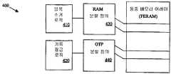
도 4는 동종 메모리 어레이(450)에 대한 메모리 분할 제어 로직(400)을 도시하고 있다. 전술한 바와 같이, 메모리 분할 제어 로직(400)은 동종 메모리가 휘발성, 비휘발성 및 프로그램 기억 장치(OTPROM) 메모리 기술처럼, 원하는 바와 같이 동작하도록 동종 메모리의 각 부분과 관련된 레지스터를 포함한다. 애플리케이션은 일반적으로 코드와 데이터에 대해 상이한 메모리 영역을 할당받는데, 그 데이터 영역은 스크래치패드 동작을 위한 휘발성 부분과 비휘발성 기억 영역으로 더 분할될 수 있다. FERAM은 본질적으로 비휘발성 어레이이다. 환언하면, FERAM은 EEPROM과 유사하게, 여러번 변경될 수 있고 심지어 전원이 제거된 경우에도 최종 기록된 값을 유지한다. 따라서, 비휘발성 어레이를 얻기 위해서 EEPROM 동작을 FERAM상에서 시행할 필요는 없다.4 illustrates memory
비휘발성 FERAM 어레이를 이용해서 휘발성 어레이를 생성하기 위해서, 소거 회로(410, 430)가 부가되는데, 이것은 예컨대 0을 각 어드레스에 기록하거나, 0을 다수의 어드레스에 병렬로 기록하는 어레이로 구현된 블록 소거 특징부를 이용한다. 소거 회로(410, 430)는 휘발성 어레이처럼 동작해야 하는 메모리 범위의 상한 및 하한을 기록한다. 유사하게, 코드가 기록되지 않도록 보장하기 위해서, 기록 잠금(lock-write) 회로(420, 440)를 이용해서 기록 금지 기능을 메모리 어레이상에 시행해야 한다. 기록 잠금 회로(420, 440)는 프로그램 기억 장치(OTPROM) 메모리처럼 동작해야 하는 메모리 범위의 상한 및 하한을 기록한다.In order to create a volatile array using a nonvolatile FERAM array, erase
애플리케이션 공간이 보안 핵심부에 의해 설정되고 나면, 동종 어레이의 정의된 영역들은 적절한 방식으로 동작할 필요가 있다. 이것은 애플리케이션에 대한 휘발성 메모리 영역을 정의하는 데 사용되는 것과 동일한 메모리 정의를 이용해서 소거 로직을 맵핑함으로써 달성될 수 있다. 애플리케이션이 시작되기 전(또는 후, 또는 전후)에 소거 매커니즘이 인에이블되어, 애플리케이션이 시작될 때 지정된 블록을 사용했을지도 모를 이전 애플리케이션 또는 보안 핵심부에 의해 남겨진 잔존 값들을 볼 수 없도록 보장한다. 유사하게, 동일하고 간단한 매커니즘을 이용해서, 애플리케이션에 대한 코드 공간으로서 지정된 영역에 기록 잠금 기능을 시행하여, 애플리케이션이 그의 코드를 변경해서 잠재적인 미지 상태를 초래하여 그 장치의 보안 상태를 드러내는 것을 방지한다.Once the application space has been set up by the security core, defined areas of the homogeneous array need to behave in a proper manner. This can be accomplished by mapping erase logic using the same memory definitions used to define the volatile memory regions for the application. The erase mechanism is enabled before (or after, or before or after the application) is started, ensuring that no residual values left by the previous application or security principal may have been seen that might have used the designated block when the application was started. Similarly, using the same simple mechanism to enforce write locking in an area designated as the code space for the application, preventing the application from changing its code resulting in a potentially unknown state, revealing the device's security state. do.
애플리케이션 RAM 영역은 소거 회로(430)에 로드되는 파라미터에 의해 정의된다. 통상적으로, 소거 회로(430)에 로드되는 값은 FERAM 메모리 어레이 내에서의 물리적인 어드레스 위치와, 할당된 메모리의 크기이다. 블록 소거 로직(410)은 그것이 가동될 때, 미리 정의된 영역을 소거하는 소거 회로(430)에 의해 속박된다. 동일한 원리가 OTP 특성을 얻는 데 사용된다. OTP 분할 처리는 기록 잠금 회로(440)에 의해 정의되는데, 그 기록 잠금 회로는 파라미터가 로드되면 동일한 메모리 어레이의 영역을 할당한다. 기록 잠금 로직(420)은 기록 잠금 회로(440)에서 정의된 영역에 대한 기록 능력을 제거함으로써, 그 영역에 OTP 메모리와 동일한 특성을 제공한다.The application RAM region is defined by parameters loaded into the erase
본원 명세서에서 제시 및 설명된 실시예 및 그 변형예는 단순히 본 발명의 원리에 대한 예시이고, 다양한 변형예가 본 발명의 기술적 사상의 범위를 벗어나는 일이 없이 당업자에 의해 실시될 수 있다.The embodiments presented and described herein and variations thereof are merely illustrative of the principles of the invention, and various modifications may be made by those skilled in the art without departing from the scope of the invention.
Claims (40)
Translated fromKoreanApplications Claiming Priority (2)
| Application Number | Priority Date | Filing Date | Title |
|---|---|---|---|
| US09/420,318 | 1999-10-19 | ||
| US09/420,318US6292874B1 (en) | 1999-10-19 | 1999-10-19 | Memory management method and apparatus for partitioning homogeneous memory and restricting access of installed applications to predetermined memory ranges |
Publications (2)
| Publication Number | Publication Date |
|---|---|
| KR20020039374A KR20020039374A (en) | 2002-05-25 |
| KR100734340B1true KR100734340B1 (en) | 2007-07-03 |
Family
ID=23665978
Family Applications (1)
| Application Number | Title | Priority Date | Filing Date |
|---|---|---|---|
| KR1020027005035AExpired - LifetimeKR100734340B1 (en) | 1999-10-19 | 2000-10-18 | Partitioned memory devices with different memory technology characteristics |
Country Status (11)
| Country | Link |
|---|---|
| US (1) | US6292874B1 (en) |
| EP (1) | EP1242891B1 (en) |
| JP (1) | JP2003523554A (en) |
| KR (1) | KR100734340B1 (en) |
| AT (1) | ATE476706T1 (en) |
| AU (1) | AU771129B2 (en) |
| CA (1) | CA2387807A1 (en) |
| DE (1) | DE60044783D1 (en) |
| IL (1) | IL149157A0 (en) |
| NZ (1) | NZ518400A (en) |
| WO (1) | WO2001029672A1 (en) |
Cited By (1)
| Publication number | Priority date | Publication date | Assignee | Title |
|---|---|---|---|---|
| US12262558B2 (en) | 2021-07-14 | 2025-03-25 | Samsung Electronics Co., Ltd. | Semiconductor device and method of manufacturing the same |
Families Citing this family (197)
| Publication number | Priority date | Publication date | Assignee | Title |
|---|---|---|---|---|
| ES2153455T3 (en) | 1995-08-04 | 2001-03-01 | Belle Gate Invest B V | DATA EXCHANGE SYSTEM THAT INCLUDES PORTABLE DATA PROCESSING UNITS. |
| US6385645B1 (en)* | 1995-08-04 | 2002-05-07 | Belle Gate Investments B.V. | Data exchange system comprising portable data processing units |
| US6295640B1 (en)* | 1998-05-08 | 2001-09-25 | Apple Computer, Inc. | Method and apparatus for distinguishing reference values from non-reference values in a runtime environment |
| AU9367098A (en)* | 1998-09-29 | 2000-04-17 | Sun Microsystems, Inc. | Superposition of data over voice |
| US6633984B2 (en)* | 1999-01-22 | 2003-10-14 | Sun Microsystems, Inc. | Techniques for permitting access across a context barrier on a small footprint device using an entry point object |
| US7093122B1 (en) | 1999-01-22 | 2006-08-15 | Sun Microsystems, Inc. | Techniques for permitting access across a context barrier in a small footprint device using shared object interfaces |
| US6907608B1 (en)* | 1999-01-22 | 2005-06-14 | Sun Microsystems, Inc. | Techniques for permitting access across a context barrier in a small footprint device using global data structures |
| US6922835B1 (en) | 1999-01-22 | 2005-07-26 | Sun Microsystems, Inc. | Techniques for permitting access across a context barrier on a small footprint device using run time environment privileges |
| US6823520B1 (en) | 1999-01-22 | 2004-11-23 | Sun Microsystems, Inc. | Techniques for implementing security on a small footprint device using a context barrier |
| CN1278236C (en) | 1999-06-10 | 2006-10-04 | 贝勒加特投资公司 | Arrangements storing different versions of a set of data in separate memory area and method for updating a set of data in a memory |
| US6772416B1 (en)* | 1999-11-19 | 2004-08-03 | General Dynamics Decision Systems, Inc. | Separation kernel with memory allocation, remote procedure call and exception handling mechanisms |
| WO2001040910A1 (en) | 1999-12-06 | 2001-06-07 | De Jong, Eduard, Karel | Computer arrangement using non-refreshed dram |
| DE69937581T2 (en) | 1999-12-07 | 2008-09-18 | Sun Microsystems, Inc., Palo Alto | COMPUTER-READABLE MEDIUM WITH MICROPROCESSOR FOR READING CONTROL AND COMPUTER ARRANGEMENT FOR COMMUNICATING WITH SUCH A MEDIUM |
| WO2001043080A1 (en)* | 1999-12-07 | 2001-06-14 | Sun Microsystems Inc. | Secure photo carrying identification device, as well as means and method for authenticating such an identification device |
| US6754815B1 (en) | 2000-03-31 | 2004-06-22 | Intel Corporation | Method and system for scrubbing an isolated area of memory after reset of a processor operating in isolated execution mode if a cleanup flag is set |
| US6678825B1 (en) | 2000-03-31 | 2004-01-13 | Intel Corporation | Controlling access to multiple isolated memories in an isolated execution environment |
| US7089418B1 (en) | 2000-03-31 | 2006-08-08 | Intel Corporation | Managing accesses in a processor for isolated execution |
| US6996710B1 (en) | 2000-03-31 | 2006-02-07 | Intel Corporation | Platform and method for issuing and certifying a hardware-protected attestation key |
| US6769058B1 (en) | 2000-03-31 | 2004-07-27 | Intel Corporation | Resetting a processor in an isolated execution environment |
| US6760441B1 (en) | 2000-03-31 | 2004-07-06 | Intel Corporation | Generating a key hieararchy for use in an isolated execution environment |
| US6957332B1 (en) | 2000-03-31 | 2005-10-18 | Intel Corporation | Managing a secure platform using a hierarchical executive architecture in isolated execution mode |
| US6934817B2 (en) | 2000-03-31 | 2005-08-23 | Intel Corporation | Controlling access to multiple memory zones in an isolated execution environment |
| US7082615B1 (en)* | 2000-03-31 | 2006-07-25 | Intel Corporation | Protecting software environment in isolated execution |
| US7356817B1 (en) | 2000-03-31 | 2008-04-08 | Intel Corporation | Real-time scheduling of virtual machines |
| US7073071B1 (en) | 2000-03-31 | 2006-07-04 | Intel Corporation | Platform and method for generating and utilizing a protected audit log |
| US7013481B1 (en) | 2000-03-31 | 2006-03-14 | Intel Corporation | Attestation key memory device and bus |
| US7194634B2 (en)* | 2000-03-31 | 2007-03-20 | Intel Corporation | Attestation key memory device and bus |
| US6633963B1 (en)* | 2000-03-31 | 2003-10-14 | Intel Corporation | Controlling access to multiple memory zones in an isolated execution environment |
| US6795905B1 (en) | 2000-03-31 | 2004-09-21 | Intel Corporation | Controlling accesses to isolated memory using a memory controller for isolated execution |
| US6990579B1 (en) | 2000-03-31 | 2006-01-24 | Intel Corporation | Platform and method for remote attestation of a platform |
| US7111176B1 (en)* | 2000-03-31 | 2006-09-19 | Intel Corporation | Generating isolated bus cycles for isolated execution |
| US7013484B1 (en)* | 2000-03-31 | 2006-03-14 | Intel Corporation | Managing a secure environment using a chipset in isolated execution mode |
| JP4771615B2 (en)* | 2000-06-02 | 2011-09-14 | コンパック インフォメーション テクノロジーズ グループ リミテッド パートナーシップ | Virtual storage system |
| US6976162B1 (en) | 2000-06-28 | 2005-12-13 | Intel Corporation | Platform and method for establishing provable identities while maintaining privacy |
| DE10033612B4 (en)* | 2000-07-11 | 2004-05-13 | Siemens Ag | Method for controlling access to a storage device |
| WO2002009046A1 (en) | 2000-07-20 | 2002-01-31 | Belle Gate Investment B.V. | Method and system of communicating devices, and devices therefor, with protected data transfer |
| US7389427B1 (en) | 2000-09-28 | 2008-06-17 | Intel Corporation | Mechanism to secure computer output from software attack using isolated execution |
| US7793111B1 (en) | 2000-09-28 | 2010-09-07 | Intel Corporation | Mechanism to handle events in a machine with isolated execution |
| FR2816090B1 (en)* | 2000-10-26 | 2003-01-10 | Schlumberger Systems & Service | DEVICE FOR SHARING FILES IN AN INTEGRATED CIRCUIT DEVICE |
| US7215781B2 (en) | 2000-12-22 | 2007-05-08 | Intel Corporation | Creation and distribution of a secret value between two devices |
| US7818808B1 (en) | 2000-12-27 | 2010-10-19 | Intel Corporation | Processor mode for limiting the operation of guest software running on a virtual machine supported by a virtual machine monitor |
| US7225441B2 (en) | 2000-12-27 | 2007-05-29 | Intel Corporation | Mechanism for providing power management through virtualization |
| US6907600B2 (en) | 2000-12-27 | 2005-06-14 | Intel Corporation | Virtual translation lookaside buffer |
| US7035963B2 (en) | 2000-12-27 | 2006-04-25 | Intel Corporation | Method for resolving address space conflicts between a virtual machine monitor and a guest operating system |
| US7117376B2 (en) | 2000-12-28 | 2006-10-03 | Intel Corporation | Platform and method of creating a secure boot that enforces proper user authentication and enforces hardware configurations |
| US6567897B2 (en)* | 2001-03-01 | 2003-05-20 | International Business Machines Corporation | Virtualized NVRAM access methods to provide NVRAM CHRP regions for logical partitions through hypervisor system calls |
| GB0106082D0 (en) | 2001-03-13 | 2001-05-02 | Mat & Separations Tech Int Ltd | Method and equipment for removing volatile compounds from air |
| US7096497B2 (en) | 2001-03-30 | 2006-08-22 | Intel Corporation | File checking using remote signing authority via a network |
| DE10127179A1 (en)* | 2001-06-05 | 2002-12-19 | Infineon Technologies Ag | Chip card memory management method has virtual addresses of defined virtual address zone assigned to physical addresses of memory locations |
| AU2002346211B2 (en) | 2001-06-27 | 2008-06-12 | Sony Corporation | Integrated circuit device, information processing device, information recording device memory management method, mobile terminal device, semiconductor integrated circuit device, and communication method using mobile terminal device |
| US7191440B2 (en)* | 2001-08-15 | 2007-03-13 | Intel Corporation | Tracking operating system process and thread execution and virtual machine execution in hardware or in a virtual machine monitor |
| US7024555B2 (en) | 2001-11-01 | 2006-04-04 | Intel Corporation | Apparatus and method for unilaterally loading a secure operating system within a multiprocessor environment |
| JP2003162433A (en)* | 2001-11-27 | 2003-06-06 | Fujitsu Ltd | Memory system |
| US20030101381A1 (en)* | 2001-11-29 | 2003-05-29 | Nikolay Mateev | System and method for virus checking software |
| US7051340B2 (en)* | 2001-11-29 | 2006-05-23 | Hewlett-Packard Development Company, L.P. | System and method for isolating applications from each other |
| US7103771B2 (en) | 2001-12-17 | 2006-09-05 | Intel Corporation | Connecting a virtual token to a physical token |
| DE10164422A1 (en)* | 2001-12-29 | 2003-07-17 | Philips Intellectual Property | Method for writing to NV memories in computer architecture, requires data values or data words to be written to specified position of cache-page register of NV memory |
| US7308576B2 (en) | 2001-12-31 | 2007-12-11 | Intel Corporation | Authenticated code module |
| DE10200288A1 (en)* | 2002-01-07 | 2003-07-17 | Scm Microsystems Gmbh | A device for executing applications that include secure transactions and / or access control to valuable content and / or services and methods for protecting such a device |
| US7480806B2 (en) | 2002-02-22 | 2009-01-20 | Intel Corporation | Multi-token seal and unseal |
| US7631196B2 (en) | 2002-02-25 | 2009-12-08 | Intel Corporation | Method and apparatus for loading a trustable operating system |
| US6912633B2 (en)* | 2002-03-18 | 2005-06-28 | Sun Microsystems, Inc. | Enhanced memory management for portable devices |
| US7181737B2 (en)* | 2002-03-18 | 2007-02-20 | Sun Microsystems, Inc. | Method and apparatus for deployment of high integrity software using static procedure return addresses |
| US7010783B2 (en)* | 2002-03-18 | 2006-03-07 | Sun Microsystems, Inc. | Method and apparatus for deployment of high integrity software using reduced dynamic memory allocation |
| US6996802B2 (en)* | 2002-03-18 | 2006-02-07 | Sun Microsystems, Inc. | Method and apparatus for deployment of high integrity software using initialization order and calling order constraints |
| US20030182653A1 (en)* | 2002-03-22 | 2003-09-25 | Giuseppe Desoli | Systems and methods for verifying correct execution of emulated code via dynamic state verification |
| US7069442B2 (en) | 2002-03-29 | 2006-06-27 | Intel Corporation | System and method for execution of a secured environment initialization instruction |
| US7028149B2 (en) | 2002-03-29 | 2006-04-11 | Intel Corporation | System and method for resetting a platform configuration register |
| US7058807B2 (en) | 2002-04-15 | 2006-06-06 | Intel Corporation | Validation of inclusion of a platform within a data center |
| US7076669B2 (en) | 2002-04-15 | 2006-07-11 | Intel Corporation | Method and apparatus for communicating securely with a token |
| US7127548B2 (en) | 2002-04-16 | 2006-10-24 | Intel Corporation | Control register access virtualization performance improvement in the virtual-machine architecture |
| KR100476892B1 (en)* | 2002-04-29 | 2005-03-17 | 삼성전자주식회사 | Tamper-resistant method and data processing system using the same |
| US7139890B2 (en) | 2002-04-30 | 2006-11-21 | Intel Corporation | Methods and arrangements to interface memory |
| GB0212315D0 (en)* | 2002-05-28 | 2002-07-10 | Symbian Ltd | Secure mobile wireless device with protected file systems |
| JP3513147B2 (en)* | 2002-05-29 | 2004-03-31 | 株式会社ハギワラシスコム | USB storage device and its control device |
| KR100505106B1 (en)* | 2002-05-29 | 2005-07-29 | 삼성전자주식회사 | Smart card with enhanced security |
| US6820177B2 (en)* | 2002-06-12 | 2004-11-16 | Intel Corporation | Protected configuration space in a protected environment |
| KR20030096659A (en) | 2002-06-17 | 2003-12-31 | 삼성전자주식회사 | Pixel array region of an image sensor, structure thereof and fabrication method thereof |
| US7142674B2 (en) | 2002-06-18 | 2006-11-28 | Intel Corporation | Method of confirming a secure key exchange |
| US7392415B2 (en) | 2002-06-26 | 2008-06-24 | Intel Corporation | Sleep protection |
| US7124327B2 (en) | 2002-06-29 | 2006-10-17 | Intel Corporation | Control over faults occurring during the operation of guest software in the virtual-machine architecture |
| US6996748B2 (en) | 2002-06-29 | 2006-02-07 | Intel Corporation | Handling faults associated with operation of guest software in the virtual-machine architecture |
| US7296267B2 (en) | 2002-07-12 | 2007-11-13 | Intel Corporation | System and method for binding virtual machines to hardware contexts |
| US8010405B1 (en) | 2002-07-26 | 2011-08-30 | Visa Usa Inc. | Multi-application smart card device software solution for smart cardholder reward selection and redemption |
| US8015060B2 (en) | 2002-09-13 | 2011-09-06 | Visa Usa, Inc. | Method and system for managing limited use coupon and coupon prioritization |
| US9852437B2 (en) | 2002-09-13 | 2017-12-26 | Visa U.S.A. Inc. | Opt-in/opt-out in loyalty system |
| US8626577B2 (en) | 2002-09-13 | 2014-01-07 | Visa U.S.A | Network centric loyalty system |
| US7121456B2 (en) | 2002-09-13 | 2006-10-17 | Visa U.S.A. Inc. | Method and system for managing token image replacement |
| GB2396713B (en)* | 2002-11-18 | 2005-09-14 | Advanced Risc Mach Ltd | Apparatus and method for controlling access to a memory unit |
| US7383587B2 (en)* | 2002-11-18 | 2008-06-03 | Arm Limited | Exception handling control in a secure processing system |
| WO2004046738A2 (en) | 2002-11-18 | 2004-06-03 | Arm Limited | Virtual to physical memory address mapping within a system having a secure domain and a non-secure domain |
| US7171539B2 (en)* | 2002-11-18 | 2007-01-30 | Arm Limited | Apparatus and method for controlling access to a memory |
| GB0226874D0 (en)* | 2002-11-18 | 2002-12-24 | Advanced Risc Mach Ltd | Switching between secure and non-secure processing modes |
| GB2396034B (en)* | 2002-11-18 | 2006-03-08 | Advanced Risc Mach Ltd | Technique for accessing memory in a data processing apparatus |
| KR101015456B1 (en)* | 2002-11-18 | 2011-02-22 | 에이알엠 리미티드 | Access control to memory by device |
| US6920611B1 (en) | 2002-11-25 | 2005-07-19 | Visa U.S.A., Inc. | Method and system for implementing a loyalty merchant component |
| US7165181B2 (en) | 2002-11-27 | 2007-01-16 | Intel Corporation | System and method for establishing trust without revealing identity |
| US7073042B2 (en)* | 2002-12-12 | 2006-07-04 | Intel Corporation | Reclaiming existing fields in address translation data structures to extend control over memory accesses |
| US7318235B2 (en) | 2002-12-16 | 2008-01-08 | Intel Corporation | Attestation using both fixed token and portable token |
| US7318141B2 (en) | 2002-12-17 | 2008-01-08 | Intel Corporation | Methods and systems to control virtual machines |
| US7793286B2 (en)* | 2002-12-19 | 2010-09-07 | Intel Corporation | Methods and systems to manage machine state in virtual machine operations |
| US7900017B2 (en) | 2002-12-27 | 2011-03-01 | Intel Corporation | Mechanism for remapping post virtual machine memory pages |
| US20040250105A1 (en)* | 2003-04-22 | 2004-12-09 | Ingo Molnar | Method and apparatus for creating an execution shield |
| US7827077B2 (en) | 2003-05-02 | 2010-11-02 | Visa U.S.A. Inc. | Method and apparatus for management of electronic receipts on portable devices |
| US20040243783A1 (en)* | 2003-05-30 | 2004-12-02 | Zhimin Ding | Method and apparatus for multi-mode operation in a semiconductor circuit |
| US7415708B2 (en) | 2003-06-26 | 2008-08-19 | Intel Corporation | Virtual machine management using processor state information |
| CN100363855C (en)* | 2003-07-04 | 2008-01-23 | 诺基亚有限公司 | Key storage management method, device and system |
| JP4537022B2 (en) | 2003-07-09 | 2010-09-01 | 株式会社日立製作所 | A data processing method, a storage area control method, and a data processing system that limit data arrangement. |
| US8554610B1 (en) | 2003-08-29 | 2013-10-08 | Visa U.S.A. Inc. | Method and system for providing reward status |
| US7104446B2 (en) | 2003-09-03 | 2006-09-12 | Visa U.S.A., Inc. | Method, system and portable consumer device using wildcard values |
| TWM249049U (en)* | 2003-09-09 | 2004-11-01 | Chicony Electronics Co Ltd | Digital camera |
| US7051923B2 (en) | 2003-09-12 | 2006-05-30 | Visa U.S.A., Inc. | Method and system for providing interactive cardholder rewards image replacement |
| US7287197B2 (en) | 2003-09-15 | 2007-10-23 | Intel Corporation | Vectoring an interrupt or exception upon resuming operation of a virtual machine |
| US7424709B2 (en) | 2003-09-15 | 2008-09-09 | Intel Corporation | Use of multiple virtual machine monitors to handle privileged events |
| US7739521B2 (en) | 2003-09-18 | 2010-06-15 | Intel Corporation | Method of obscuring cryptographic computations |
| US7610611B2 (en) | 2003-09-19 | 2009-10-27 | Moran Douglas R | Prioritized address decoder |
| US20050071656A1 (en)* | 2003-09-25 | 2005-03-31 | Klein Dean A. | Secure processor-based system and method |
| US7681046B1 (en) | 2003-09-26 | 2010-03-16 | Andrew Morgan | System with secure cryptographic capabilities using a hardware specific digital secret |
| US7366305B2 (en) | 2003-09-30 | 2008-04-29 | Intel Corporation | Platform and method for establishing trust without revealing identity |
| US8407083B2 (en) | 2003-09-30 | 2013-03-26 | Visa U.S.A., Inc. | Method and system for managing reward reversal after posting |
| US20050080934A1 (en) | 2003-09-30 | 2005-04-14 | Cota-Robles Erik C. | Invalidating translation lookaside buffer entries in a virtual machine (VM) system |
| US7177967B2 (en) | 2003-09-30 | 2007-02-13 | Intel Corporation | Chipset support for managing hardware interrupts in a virtual machine system |
| US8005763B2 (en) | 2003-09-30 | 2011-08-23 | Visa U.S.A. Inc. | Method and system for providing a distributed adaptive rules based dynamic pricing system |
| US7237051B2 (en) | 2003-09-30 | 2007-06-26 | Intel Corporation | Mechanism to control hardware interrupt acknowledgement in a virtual machine system |
| US7149863B1 (en)* | 2003-10-08 | 2006-12-12 | Sun Microsystems, Inc. | System and method of descriptively specifying memory placement in a computer system |
| DE10347828A1 (en)* | 2003-10-10 | 2005-05-25 | Giesecke & Devrient Gmbh | Accessing data items in a portable disk |
| US20070083726A1 (en)* | 2003-10-13 | 2007-04-12 | Koninklijke Philips Electronics N.V. | Storage allocation per application |
| US7653602B2 (en) | 2003-11-06 | 2010-01-26 | Visa U.S.A. Inc. | Centralized electronic commerce card transactions |
| US7636844B2 (en) | 2003-11-17 | 2009-12-22 | Intel Corporation | Method and system to provide a trusted channel within a computer system for a SIM device |
| US7694151B1 (en)* | 2003-11-20 | 2010-04-06 | Johnson Richard C | Architecture, system, and method for operating on encrypted and/or hidden information |
| US8156343B2 (en) | 2003-11-26 | 2012-04-10 | Intel Corporation | Accessing private data about the state of a data processing machine from storage that is publicly accessible |
| US8037314B2 (en) | 2003-12-22 | 2011-10-11 | Intel Corporation | Replacing blinded authentication authority |
| US7802085B2 (en) | 2004-02-18 | 2010-09-21 | Intel Corporation | Apparatus and method for distributing private keys to an entity with minimal secret, unique information |
| US7356735B2 (en) | 2004-03-30 | 2008-04-08 | Intel Corporation | Providing support for single stepping a virtual machine in a virtual machine environment |
| US7620949B2 (en) | 2004-03-31 | 2009-11-17 | Intel Corporation | Method and apparatus for facilitating recognition of an open event window during operation of guest software in a virtual machine environment |
| DE602005007531D1 (en)* | 2004-04-09 | 2008-07-31 | Proton World Int Nv | Shared file access to indivisible files |
| US7490070B2 (en) | 2004-06-10 | 2009-02-10 | Intel Corporation | Apparatus and method for proving the denial of a direct proof signature |
| US7305592B2 (en) | 2004-06-30 | 2007-12-04 | Intel Corporation | Support for nested fault in a virtual machine environment |
| US7840962B2 (en) | 2004-09-30 | 2010-11-23 | Intel Corporation | System and method for controlling switching between VMM and VM using enabling value of VMM timer indicator and VMM timer value having a specified time |
| US8146078B2 (en) | 2004-10-29 | 2012-03-27 | Intel Corporation | Timer offsetting mechanism in a virtual machine environment |
| CN100489818C (en)* | 2004-11-26 | 2009-05-20 | 松下电器产业株式会社 | Processor and secure processing system |
| US8924728B2 (en) | 2004-11-30 | 2014-12-30 | Intel Corporation | Apparatus and method for establishing a secure session with a device without exposing privacy-sensitive information |
| US8533777B2 (en) | 2004-12-29 | 2013-09-10 | Intel Corporation | Mechanism to determine trust of out-of-band management agents |
| DE102005000796A1 (en)* | 2005-01-05 | 2006-07-13 | Giesecke & Devrient Gmbh | Portable media with watermark functionality |
| US7395405B2 (en) | 2005-01-28 | 2008-07-01 | Intel Corporation | Method and apparatus for supporting address translation in a virtual machine environment |
| KR100704037B1 (en)* | 2005-04-15 | 2007-04-04 | 삼성전자주식회사 | Data storage device having heterogeneous nonvolatile memory and its driving method |
| US7406711B2 (en)* | 2005-09-02 | 2008-07-29 | Motorola, Inc. | Method and apparatus for enforcing independence of processors on a single IC |
| US7809957B2 (en) | 2005-09-29 | 2010-10-05 | Intel Corporation | Trusted platform module for generating sealed data |
| US9573067B2 (en)* | 2005-10-14 | 2017-02-21 | Microsoft Technology Licensing, Llc | Mass storage in gaming handhelds |
| US7496727B1 (en) | 2005-12-06 | 2009-02-24 | Transmeta Corporation | Secure memory access system and method |
| US7845005B2 (en)* | 2006-02-07 | 2010-11-30 | International Business Machines Corporation | Method for preventing malicious software installation on an internet-connected computer |
| US8014530B2 (en) | 2006-03-22 | 2011-09-06 | Intel Corporation | Method and apparatus for authenticated, recoverable key distribution with no database secrets |
| US7650479B2 (en)* | 2006-09-20 | 2010-01-19 | Arm Limited | Maintaining cache coherency for secure and non-secure data access requests |
| US20080077749A1 (en)* | 2006-09-22 | 2008-03-27 | Daniel Scott Cohen | Access control of memory space in microprocessor systems |
| FR2908916B1 (en)* | 2006-11-17 | 2009-04-17 | Thales Sa | GRAPHIC OBJECT PROCESSING SYSTEM COMPRISING A SECURE GRAPHIC MANAGER |
| SG146551A1 (en)* | 2007-03-29 | 2008-10-30 | Toshiba Kk | Portable electronic device and control method of portable electronic device |
| EP1978447B1 (en) | 2007-04-05 | 2011-02-16 | STMicroelectronics (Research & Development) Limited | Integrated circuit with restricted data access |
| US20080270652A1 (en)* | 2007-04-30 | 2008-10-30 | Jeffrey Kevin Jeansonne | System and method of tamper-resistant control |
| US8213612B2 (en)* | 2007-12-07 | 2012-07-03 | Inside Contactless S.A. | Secure software download |
| FR2929729A1 (en)* | 2008-04-03 | 2009-10-09 | Alveol Technology Sarl | DEVICE FOR MANAGING THE MEMORY OF A COMPUTER ENVIRONMENT |
| US20120042147A1 (en)* | 2008-09-22 | 2012-02-16 | France Telecom | Memory allocation method and a method for managing data related to an application stored in a security module associated with a terminal, an associated security module and an associated terminal |
| KR101481562B1 (en)* | 2008-09-22 | 2015-01-13 | 엘지전자 주식회사 | Digital broadcast receiving apparatus and method for setting its operation memory |
| KR101573047B1 (en) | 2009-01-23 | 2015-12-02 | 삼성전자주식회사 | Complex memory device and I/O processing method using these |
| RU2422883C1 (en)* | 2009-12-09 | 2011-06-27 | Корпорация "САМСУНГ ЭЛЕКТРОНИКС Ко., Лтд." | System and method of arranging static data objects in heterogeneous random-access memory |
| US7992781B2 (en) | 2009-12-16 | 2011-08-09 | Visa International Service Association | Merchant alerts incorporating receipt data |
| US8429048B2 (en) | 2009-12-28 | 2013-04-23 | Visa International Service Association | System and method for processing payment transaction receipts |
| KR101119434B1 (en)* | 2010-05-26 | 2012-03-16 | 주식회사 켐트로닉스 | Micro controller unit sharing one memory, method for controlling memory included therein and computer readable record-midium on which program for excuting method thereof |
| US8539245B2 (en)* | 2010-08-06 | 2013-09-17 | Intel Corporation | Apparatus and method for accessing a secure partition in non-volatile storage by a host system enabled after the system exits a first instance of a secure mode |
| CN107608910B (en) | 2011-09-30 | 2021-07-02 | 英特尔公司 | Apparatus and method for implementing a multi-level memory hierarchy with different operating modes |
| CN108549609B (en)* | 2011-09-30 | 2022-06-21 | 英特尔公司 | Non-volatile random access memory (NVRAM) as a replacement for conventional mass storage devices |
| WO2013048491A1 (en) | 2011-09-30 | 2013-04-04 | Intel Corporation | Apparatus, method and system that stores bios in non-volatile random access memory |
| EP2761468B1 (en)* | 2011-09-30 | 2019-12-11 | Intel Corporation | Platform storage hierarchy with non-volatile random access memory having configurable partitions |
| EP3364304B1 (en) | 2011-09-30 | 2022-06-15 | INTEL Corporation | Memory channel that supports near memory and far memory access |
| EP2761465B1 (en) | 2011-09-30 | 2022-02-09 | Intel Corporation | Autonomous initialization of non-volatile random access memory in a computer system |
| US8667270B2 (en) | 2012-02-10 | 2014-03-04 | Samsung Electronics Co., Ltd. | Securely upgrading or downgrading platform components |
| US9286235B2 (en)* | 2012-06-29 | 2016-03-15 | Intel Corporation | Virtual memory address range register |
| US9075751B2 (en)* | 2012-08-09 | 2015-07-07 | Intel Corporation | Secure data protection with improved read-only memory locking during system pre-boot |
| KR102002900B1 (en) | 2013-01-07 | 2019-07-23 | 삼성전자 주식회사 | System on chip including memory management unit and memory address translation method thereof |
| US9224452B2 (en) | 2013-01-17 | 2015-12-29 | Qualcomm Incorporated | Heterogeneous memory systems, and related methods and computer-readable media for supporting heterogeneous memory access requests in processor-based systems |
| KR102088403B1 (en) | 2013-08-08 | 2020-03-13 | 삼성전자 주식회사 | Storage device, computer system comprising the same, and operating method thereof |
| US20160048353A1 (en)* | 2014-08-13 | 2016-02-18 | Kabushiki Kaisha Toshiba | Memory system and method of controlling memory system |
| DE102015200801A1 (en)* | 2015-01-20 | 2016-07-21 | Continental Teves Ag & Co. Ohg | Electronic control device |
| US9405515B1 (en)* | 2015-02-04 | 2016-08-02 | Rockwell Collins, Inc. | Computing systems utilizing controlled dynamic libraries and isolated execution spaces |
| US9904586B2 (en)* | 2015-10-28 | 2018-02-27 | Intel Corporation | Interfacing with block-based storage in a processor |
| US9747041B2 (en) | 2015-12-23 | 2017-08-29 | Intel Corporation | Apparatus and method for a non-power-of-2 size cache in a first level memory device to cache data present in a second level memory device |
| US10007606B2 (en) | 2016-03-30 | 2018-06-26 | Intel Corporation | Implementation of reserved cache slots in computing system having inclusive/non inclusive tracking and two level system memory |
| US10185619B2 (en) | 2016-03-31 | 2019-01-22 | Intel Corporation | Handling of error prone cache line slots of memory side cache of multi-level system memory |
| US10120806B2 (en) | 2016-06-27 | 2018-11-06 | Intel Corporation | Multi-level system memory with near memory scrubbing based on predicted far memory idle time |
| CN107665175A (en)* | 2016-07-27 | 2018-02-06 | 展讯通信(上海)有限公司 | The method, apparatus and electronic equipment of memory partition isolation |
| US10915453B2 (en) | 2016-12-29 | 2021-02-09 | Intel Corporation | Multi level system memory having different caching structures and memory controller that supports concurrent look-up into the different caching structures |
| US10445261B2 (en) | 2016-12-30 | 2019-10-15 | Intel Corporation | System memory having point-to-point link that transports compressed traffic |
| US10304814B2 (en) | 2017-06-30 | 2019-05-28 | Intel Corporation | I/O layout footprint for multiple 1LM/2LM configurations |
| US11188467B2 (en) | 2017-09-28 | 2021-11-30 | Intel Corporation | Multi-level system memory with near memory capable of storing compressed cache lines |
| US10860244B2 (en) | 2017-12-26 | 2020-12-08 | Intel Corporation | Method and apparatus for multi-level memory early page demotion |
| US20190258812A1 (en)* | 2018-02-20 | 2019-08-22 | Sensata Technologies, Inc. | Memory security for automotive functional safety compliance with independent downstream processes |
| KR102745459B1 (en) | 2018-12-18 | 2024-12-20 | 에스케이하이닉스 주식회사 | Smart car system |
| US11055228B2 (en) | 2019-01-31 | 2021-07-06 | Intel Corporation | Caching bypass mechanism for a multi-level memory |
Citations (3)
| Publication number | Priority date | Publication date | Assignee | Title |
|---|---|---|---|---|
| US4930129A (en) | 1987-03-13 | 1990-05-29 | Mitsubishi Denki Kabushiki Kaisha | IC card having internal error checking capability |
| US5890199A (en) | 1996-10-21 | 1999-03-30 | Ramtron International Corporation | Data processor incorporating a ferroelectric memory array selectably configurable as read/write and read only memory |
| US5912453A (en) | 1995-09-29 | 1999-06-15 | International Business Machines Corporation | Multiple application chip card with decoupled programs |
Family Cites Families (7)
| Publication number | Priority date | Publication date | Assignee | Title |
|---|---|---|---|---|
| JP2682700B2 (en)* | 1989-05-09 | 1997-11-26 | 三菱電機株式会社 | IC card |
| JPH03276337A (en)* | 1990-03-27 | 1991-12-06 | Toshiba Corp | Microcontroller |
| JP3178881B2 (en)* | 1992-03-06 | 2001-06-25 | 株式会社東芝 | Portable electronic devices |
| JPH05120891A (en)* | 1992-04-24 | 1993-05-18 | Hitachi Ltd | Semiconductor storage device |
| JPH06274397A (en)* | 1993-03-24 | 1994-09-30 | Toshiba Corp | File management method |
| JPH07114497A (en)* | 1993-10-14 | 1995-05-02 | Hitachi Ltd | Semiconductor integrated circuit device |
| US5818771A (en)* | 1996-09-30 | 1998-10-06 | Hitachi, Ltd. | Semiconductor memory device |
- 1999
- 1999-10-19USUS09/420,318patent/US6292874B1/ennot_activeExpired - Lifetime
- 2000
- 2000-10-18JPJP2001532399Apatent/JP2003523554A/enactivePending
- 2000-10-18ATAT00984535Tpatent/ATE476706T1/ennot_activeIP Right Cessation
- 2000-10-18EPEP00984535Apatent/EP1242891B1/ennot_activeExpired - Lifetime
- 2000-10-18WOPCT/US2000/041243patent/WO2001029672A1/enactiveIP Right Grant
- 2000-10-18DEDE60044783Tpatent/DE60044783D1/ennot_activeExpired - Lifetime
- 2000-10-18AUAU21137/01Apatent/AU771129B2/ennot_activeCeased
- 2000-10-18NZNZ518400Apatent/NZ518400A/enunknown
- 2000-10-18ILIL14915700Apatent/IL149157A0/enunknown
- 2000-10-18KRKR1020027005035Apatent/KR100734340B1/ennot_activeExpired - Lifetime
- 2000-10-18CACA002387807Apatent/CA2387807A1/ennot_activeAbandoned
Patent Citations (3)
| Publication number | Priority date | Publication date | Assignee | Title |
|---|---|---|---|---|
| US4930129A (en) | 1987-03-13 | 1990-05-29 | Mitsubishi Denki Kabushiki Kaisha | IC card having internal error checking capability |
| US5912453A (en) | 1995-09-29 | 1999-06-15 | International Business Machines Corporation | Multiple application chip card with decoupled programs |
| US5890199A (en) | 1996-10-21 | 1999-03-30 | Ramtron International Corporation | Data processor incorporating a ferroelectric memory array selectably configurable as read/write and read only memory |
Cited By (1)
| Publication number | Priority date | Publication date | Assignee | Title |
|---|---|---|---|---|
| US12262558B2 (en) | 2021-07-14 | 2025-03-25 | Samsung Electronics Co., Ltd. | Semiconductor device and method of manufacturing the same |
Also Published As
| Publication number | Publication date |
|---|---|
| ATE476706T1 (en) | 2010-08-15 |
| KR20020039374A (en) | 2002-05-25 |
| WO2001029672A1 (en) | 2001-04-26 |
| WO2001029672A9 (en) | 2002-08-08 |
| IL149157A0 (en) | 2002-11-10 |
| US6292874B1 (en) | 2001-09-18 |
| EP1242891B1 (en) | 2010-08-04 |
| DE60044783D1 (en) | 2010-09-16 |
| AU771129B2 (en) | 2004-03-11 |
| JP2003523554A (en) | 2003-08-05 |
| EP1242891A4 (en) | 2008-08-13 |
| EP1242891A1 (en) | 2002-09-25 |
| AU2113701A (en) | 2001-04-30 |
| CA2387807A1 (en) | 2001-04-26 |
| NZ518400A (en) | 2003-01-31 |
Similar Documents
| Publication | Publication Date | Title |
|---|---|---|
| KR100734340B1 (en) | Partitioned memory devices with different memory technology characteristics | |
| JP2727520B2 (en) | Memory card and operating method thereof | |
| CN112602061B (en) | Domain crossing when executing instructions in a computer processor | |
| CN112602060B (en) | Virtual machine registers in a computer processor | |
| KR102095614B1 (en) | Memory protection | |
| US7975117B2 (en) | Enforcing isolation among plural operating systems | |
| US10923203B2 (en) | Semiconductor device and method of operating semiconductor device | |
| CN112639779A (en) | Security configuration for translation of memory addresses from object-specific virtual address space to physical address space | |
| CN112639732A (en) | Dynamic configuration of computer processors based on presence of hypervisors | |
| CN110968254B (en) | Partition protection method and device for nonvolatile memory | |
| JP3878134B2 (en) | Microprocessor circuit for data carrier and method for organizing access to data stored in memory | |
| KR20050113659A (en) | Universal memory device having a profile storage unit | |
| US20020128994A1 (en) | Method of tracking objects for application modifications | |
| GB2356469A (en) | Portable data carrier memory management system and method | |
| KR20020078998A (en) | Smart card capable of maintenence security between multi-application programs |
Legal Events
| Date | Code | Title | Description |
|---|---|---|---|
| PA0105 | International application | Patent event date:20020419 Patent event code:PA01051R01D Comment text:International Patent Application | |
| PG1501 | Laying open of application | ||
| A201 | Request for examination | ||
| PA0201 | Request for examination | Patent event code:PA02012R01D Patent event date:20051018 Comment text:Request for Examination of Application | |
| N231 | Notification of change of applicant | ||
| PN2301 | Change of applicant | Patent event date:20060502 Comment text:Notification of Change of Applicant Patent event code:PN23011R01D | |
| E902 | Notification of reason for refusal | ||
| PE0902 | Notice of grounds for rejection | Comment text:Notification of reason for refusal Patent event date:20061117 Patent event code:PE09021S01D | |
| E701 | Decision to grant or registration of patent right | ||
| PE0701 | Decision of registration | Patent event code:PE07011S01D Comment text:Decision to Grant Registration Patent event date:20070530 | |
| GRNT | Written decision to grant | ||
| PR0701 | Registration of establishment | Comment text:Registration of Establishment Patent event date:20070626 Patent event code:PR07011E01D | |
| PR1002 | Payment of registration fee | Payment date:20070627 End annual number:3 Start annual number:1 | |
| PG1601 | Publication of registration | ||
| PR1001 | Payment of annual fee | Payment date:20100625 Start annual number:4 End annual number:4 | |
| PR1001 | Payment of annual fee | Payment date:20110519 Start annual number:5 End annual number:5 | |
| PR1001 | Payment of annual fee | Payment date:20120611 Start annual number:6 End annual number:6 | |
| FPAY | Annual fee payment | Payment date:20130612 Year of fee payment:7 | |
| PR1001 | Payment of annual fee | Payment date:20130612 Start annual number:7 End annual number:7 | |
| FPAY | Annual fee payment | Payment date:20140611 Year of fee payment:8 | |
| PR1001 | Payment of annual fee | Payment date:20140611 Start annual number:8 End annual number:8 | |
| FPAY | Annual fee payment | Payment date:20150608 Year of fee payment:9 | |
| PR1001 | Payment of annual fee | Payment date:20150608 Start annual number:9 End annual number:9 | |
| FPAY | Annual fee payment | Payment date:20160616 Year of fee payment:10 | |
| PR1001 | Payment of annual fee | Payment date:20160616 Start annual number:10 End annual number:10 | |
| FPAY | Annual fee payment | Payment date:20170614 Year of fee payment:11 | |
| PR1001 | Payment of annual fee | Payment date:20170614 Start annual number:11 End annual number:11 | |
| FPAY | Annual fee payment | Payment date:20180601 Year of fee payment:12 | |
| PR1001 | Payment of annual fee | Payment date:20180601 Start annual number:12 End annual number:12 | |
| PC1801 | Expiration of term | Termination date:20210418 Termination category:Expiration of duration |