KR100734058B1 - Organic EL device and method of manufacturing polarizing plate used therein - Google Patents
Organic EL device and method of manufacturing polarizing plate used thereinDownload PDFInfo
- Publication number
- KR100734058B1 KR100734058B1KR1020060030260AKR20060030260AKR100734058B1KR 100734058 B1KR100734058 B1KR 100734058B1KR 1020060030260 AKR1020060030260 AKR 1020060030260AKR 20060030260 AKR20060030260 AKR 20060030260AKR 100734058 B1KR100734058 B1KR 100734058B1
- Authority
- KR
- South Korea
- Prior art keywords
- substrate
- polarizing plate
- electrode layer
- mask
- organic
- Prior art date
- Legal status (The legal status is an assumption and is not a legal conclusion. Google has not performed a legal analysis and makes no representation as to the accuracy of the status listed.)
- Active
Links
Images


Classifications
- H—ELECTRICITY
- H10—SEMICONDUCTOR DEVICES; ELECTRIC SOLID-STATE DEVICES NOT OTHERWISE PROVIDED FOR
- H10K—ORGANIC ELECTRIC SOLID-STATE DEVICES
- H10K50/00—Organic light-emitting devices
- H10K50/80—Constructional details
- H10K50/86—Arrangements for improving contrast, e.g. preventing reflection of ambient light
- H—ELECTRICITY
- H10—SEMICONDUCTOR DEVICES; ELECTRIC SOLID-STATE DEVICES NOT OTHERWISE PROVIDED FOR
- H10K—ORGANIC ELECTRIC SOLID-STATE DEVICES
- H10K50/00—Organic light-emitting devices
- H10K50/80—Constructional details
- H10K50/805—Electrodes
- H—ELECTRICITY
- H10—SEMICONDUCTOR DEVICES; ELECTRIC SOLID-STATE DEVICES NOT OTHERWISE PROVIDED FOR
- H10K—ORGANIC ELECTRIC SOLID-STATE DEVICES
- H10K50/00—Organic light-emitting devices
- H10K50/80—Constructional details
- H10K50/85—Arrangements for extracting light from the devices
- H—ELECTRICITY
- H10—SEMICONDUCTOR DEVICES; ELECTRIC SOLID-STATE DEVICES NOT OTHERWISE PROVIDED FOR
- H10K—ORGANIC ELECTRIC SOLID-STATE DEVICES
- H10K71/00—Manufacture or treatment specially adapted for the organic devices covered by this subclass
Landscapes
- Physics & Mathematics (AREA)
- Optics & Photonics (AREA)
- Engineering & Computer Science (AREA)
- Manufacturing & Machinery (AREA)
- Electroluminescent Light Sources (AREA)
Abstract
Description
Translated fromKorean도 1은 종래의 유기 전계 발광 소자를 도시한 단면도이다.1 is a cross-sectional view showing a conventional organic electroluminescent device.
도 2는 종래의 유기 전계 발광 소자에 편광판을 부착하는 과정을 도시한 사시도이다.2 is a perspective view illustrating a process of attaching a polarizing plate to a conventional organic EL device.
도 3은 본 발명의 바람직한 일 실시예에 따른 유기 전계 발광 소자를 도시한 단면도이다.3 is a cross-sectional view illustrating an organic EL device according to an exemplary embodiment of the present invention.
도 4는 도 3의 편광판을 도시한 정면도이다.4 is a front view illustrating the polarizer of FIG. 3.
도 5a 내지 5f는 도 3의 편광판의 제조과정을 도시한 사시도들이다.5A through 5F are perspective views illustrating a manufacturing process of the polarizing plate of FIG. 3.
본 발명은 유기 전계 발광 소자에 사용되는 편광판의 제조방법에 관한 것으로, 더욱 상세하게는 유기 전계 발광 소자의 발광시 휘도를 증가시킬 수 있는 유기 전계 발광 소자 및 이에 사용되는 편광판의 제조방법에 관한 것이다.The present invention relates to a method of manufacturing a polarizing plate used in an organic electroluminescent device, and more particularly, to an organic electroluminescent device capable of increasing luminance when emitting an organic electroluminescent device and a method of manufacturing a polarizing plate used therein. .
유기 전계 발광 소자는 소정 전압이 인가된 경우 소정 파장을 가지는 빛을 발생시킨다.The organic EL device generates light having a predetermined wavelength when a predetermined voltage is applied.
도 1은 종래의 유기 전계 발광 소자를 도시한 단면도이고, 도 2는 종래의 유기 전계 발광 소자에 편광판을 부착하는 과정을 도시한 사시도이다.1 is a cross-sectional view illustrating a conventional organic electroluminescent device, and FIG. 2 is a perspective view illustrating a process of attaching a polarizing plate to a conventional organic electroluminescent device.
도 1을 참조하면, 종래의 유기 전계 발광 소자(100)는 기판(102), 애노드 전극층(104), 유기물층(106), 캐소드 전극층(108) 및 편광판(110)을 포함한다.Referring to FIG. 1, the conventional
애노드 전극층(104)에 소정의 양의 전압이 인가되고 캐소드 전극층(108)에 소정의 음의 전압이 인가된 경우, 유기물층(106)은 소정 파장을 가지는 빛을 발생시킨다.When a predetermined positive voltage is applied to the
유기물층(106)으로부터 발생된 빛은 편광판(110)을 통과하여 외부로 발산된다.Light generated from the
편광판(110)은 특정한 색을 띄는 반투명 소자이며, 기판(102)의 하면에 부착된다.The
도 2를 참조하면, 기판(102)의 상면에 애노드 전극층(104), 유기물층(106) 및 캐소드 전극층(108)이 순차적으로 형성된 후, 기판(102)의 하면에 편광판(110)이 부착되는 공정이 수행된다.2, after the
이 경우, 편광판(110)은 기판(102)의 하면에 정확하게 부착되어야 한다. 그러나, 편광판(110)을 기판(102)의 하면에 부착시 오차가 많이 발생한다.In this case, the
또한, 편광판(110)은 특정한 색, 예를 들면 검은색, 붉은색 등을 띄는 소자로 구성된다.In addition, the
한편, 유기 전계 발광 소자(100)는 R픽셀, G픽셀 및 B픽셀의 휘도 특성이 각각 다르다. 이에 따라, 동일한 휘도를 구현하기 위해서는 상기 각 픽셀에 인가되어야 하는 전류도 달라진다.On the other hand, the
이와 같이, 특정한 하나의 색을 띄는 편광판(110)을 통과하면, R픽셀, G픽셀 및 B픽셀 중 어느 하나의 픽셀의 휘도 특성은 좋아지나, 나머지 픽셀들의 휘도 특성은 저하된다. 즉, 나머지 픽셀들의 휘도 특성을 증가시키기 위해 더 많은 전류가 상기 픽셀들에 인가되어야 한다.As such, when passing through the polarizing
또한, 기판(102)을 통과한 빛은 편광판(110)을 다시 한번 통과하므로 빛의 휘도가 감소되고, 소자의 두께가 증가하여 박막형 디스플레이 소자 구현에 어려움이 있었다.In addition, since the light passing through the
게다가, 상기 R, G 및 B픽셀들을 발광하기 위하여는 많은 전류가 필요하게 된다.In addition, a large amount of current is required to emit the R, G, and B pixels.
따라서, 유기 전계 발광 소자(100)의 소비전력이 증가하고, 수명이 단축되는 문제점이 있었다.Therefore, the power consumption of the
본 발명의 목적은 기판 하부에 직접 편광판을 형성하여 소자의 두께가 얇아지고 휘도를 향상시킬 수 있는 유기 전계 발광 소자 및 이에 사용되는 편광판의 제조방법을 제공하는 것이다.SUMMARY OF THE INVENTION An object of the present invention is to provide an organic electroluminescent device capable of forming a polarizing plate directly under a substrate and improving thickness of the device and improving luminance, and a method of manufacturing the polarizing plate used therein.
또한 본 발명의 목적은 유기 전계 발광 소자의 발광시 필요한 전체 전류를 감소시켜 소비전력을 최소화할 수 있는 유기 전계 발광 소자 및 이에 사용되는 편 광판의 제조방법을 제공하는 것이다.It is also an object of the present invention to provide an organic electroluminescent device capable of minimizing power consumption by reducing the total current required to emit light of an organic electroluminescent device and a method of manufacturing a polarizing plate used therein.
또한 본 발명의 목적은 픽셀들의 휘도 특성에 따라 특정 색을 띠는 물질들로 형성된 편광판을 사용하여 유기 전계 발광 소자의 발광시 필요한 전류를 감소시키고 휘도 특성을 증가시킬 수 있는 유기 전계 발광 소자 및 이에 사용되는 편광판의 제조방법을 제공하는 것이다.In addition, an object of the present invention is to use an polarizing plate formed of materials having a specific color according to the luminance characteristics of the pixels and to reduce the electric current required to emit light of the organic electroluminescent element and to increase the luminance characteristic thereof. It is to provide a method for producing a polarizing plate to be used.
상기한 바와 같은 목적을 달성하기 위하여, 본 발명의 바람직한 일 실시예에 따른 발광 소자는 기판, 상기 기판의 일 표면에 형성되는 애노드 전극층, 상기 애노드 전극층 위에 형성되는 발광층, 상기 발광층 위에 형성되는 캐소드 전극층, 및 상기 기판의 한 면에 형성되는 편광판을 포함하되, 상기 편광판은 상기 발광층에서 발광되는 각 빛의 색들과 상응하는 유색의 물질들로 형성되는 것을 특징으로 한다.In order to achieve the above object, a light emitting device according to an embodiment of the present invention is a substrate, an anode electrode layer formed on one surface of the substrate, a light emitting layer formed on the anode electrode layer, a cathode electrode layer formed on the light emitting layer And a polarizing plate formed on one surface of the substrate, wherein the polarizing plate is formed of colored materials corresponding to colors of each light emitted from the light emitting layer.
또한 본 발명에 따른 유기 전계 발광 소자의 편광판 제조방법은 애노드 전극층, 유기물층 및 캐소드 전극층이 형성된 기판의 하면에 상기 유기물층의 제 1 유기물과 대응되는 제 1 유색 물질을 형성하는 제 1 단계, 상기 제 1 유색 물질이 형성된 기판의 하면에 상기 유기물층의 제 2 유기물과 대응되는 제 2 유색 물질을 형성하는 제 2 단계 및 상기 제 1 및 제 2 유색 물질이 형성된 기판의 하면에 상기 유기물층의 제 3 유기물과 대응되는 제 3 유색 물질을 형성하는 제 3 단계를 포함한다.In addition, the method of manufacturing a polarizing plate of an organic EL device according to the present invention comprises a first step of forming a first colored material corresponding to the first organic material of the organic material layer on the lower surface of the substrate on which the anode electrode layer, the organic material layer and the cathode electrode layer are formed; A second step of forming a second colored material corresponding to the second organic material of the organic material layer on the lower surface of the substrate on which the colored material is formed and corresponding to the third organic material of the organic material layer on the lower surface of the substrate on which the first and second colored materials are formed; And a third step of forming a third colored material.
상기 유기 전계 발광 소자 및 이에 사용되는 편광판의 제조방법은 유기 전계 발광 소자의 발광시 필요한 전체 전류를 감소시켜 소비전력을 최소화하고 휘도 특 성을 증가시킬 수 있다.The method of manufacturing the organic EL device and the polarizing plate used therein may reduce the total current required to emit light of the organic EL device, thereby minimizing power consumption and increasing luminance characteristics.
이하에서는 첨부된 도면들을 참조하여 본 발명에 따른 유기 전계 발광 소자 및 이에 사용되는 편광판의 제조방법의 바람직한 실시예를 자세히 설명하도록 한다.Hereinafter, with reference to the accompanying drawings will be described in detail a preferred embodiment of the organic electroluminescent device according to the present invention and a method of manufacturing a polarizing plate used therein.
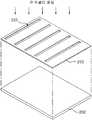
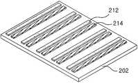
도 3은 본 발명의 바람직한 일 실시예에 따른 유기 전계 발광 소자를 도시한 단면도이고, 도 4는 도 3의 편광판을 도시한 정면도이다.3 is a cross-sectional view illustrating an organic EL device according to an exemplary embodiment of the present invention, and FIG. 4 is a front view illustrating the polarizer of FIG. 3.
도 3을 참조하면, 본 발명의 유기 전계 발광 소자(200)는 기판(202), 애노드 전극층(204), 유기물층(206), 캐소드 전극층(208) 및 편광판(210)을 포함한다.Referring to FIG. 3, the organic
애노드 전극층(204)은 예를 들어, 증착 공정에 의해 기판(202) 위에 형성된다.The
유기물층(206)은 예를 들어, 증착 공정에 의해 애노드 전극층(204) 위에 형성되며, 정공주입층(Hole Injection Layer, HIL), 정공수송층(Hole Transporting Layer, HTL), 발광층(Emitting Layer, EML), 전자수송층(Electron Transporting Layer, ETL) 및 전자주입층(Electron Injection Layer, EIL)을 포함한다.The
캐소드 전극층(208)은 금속, 예를 들어 알루미늄(aluminum, Al)으로 이루어지며, 유기물층(206) 위에 예를 들어, 증착 공정에 의해 형성된다.The
이하, 상기 유기 전계 발광 소자(200)의 발광 동작을 상술하겠다.Hereinafter, the light emission operation of the
애노드 전극층(204)에 소정의 양의 전압이 인가된 경우, 애노드 전극층(204)은 정공들을 상기 정공주입층에 제공한다. 캐소드 전극층(208)에 소정의 음의 전압 이 인가된 경우, 캐소드 전극층(208)은 전자들을 상기 전자주입층에 제공한다.When a predetermined amount of voltage is applied to the
이어서, 상기 정공주입층은 상기 애노드 전극층(204)으로부터 제공된 정공들을 상기 정공수송층으로 원활하게 주입하며, 상기 전자주입층은 상기 캐소드 전극층(208)으로부터 제공된 전자들을 상기 전자수송층으로 원활하게 주입한다.Subsequently, the hole injection layer smoothly injects holes provided from the
계속하여, 상기 정공수송층은 상기 정공주입층으로부터 주입된 정공들을 상기 발광층으로 수송하고, 상기 전자수송층은 상기 전자주입층으로부터 주입된 전자들을 상기 발광층으로 수송한다.Subsequently, the hole transport layer transports holes injected from the hole injection layer to the light emitting layer, and the electron transport layer transports electrons injected from the electron injection layer to the light emitting layer.
이어서, 상기 발광층으로 수송된 정공들 및 전자들이 재결합하여 특정 파장을 가지는 빛을 발생시킨다.Subsequently, holes and electrons transported to the emission layer recombine to generate light having a specific wavelength.
계속하여, 상기 발광층으로부터 발생된 빛은 기판(202) 및 편광판(210)을 투과하여 외부로 발산된다.Subsequently, the light generated from the light emitting layer is transmitted through the
편광판(210)은 도 3에 도시된 바와 같이, 애노드 전극층(204)이 형성되는 기판(202)의 상면과 상반되는 기판(202)의 표면, 즉 저면에 형성되어, 상기 발광층으로부터 발생된 빛을 소정의 투과율을 가지고 통과시킨다.As illustrated in FIG. 3, the polarizing
그러나, 편광판(210)이 다른 위치에 형성될 수 있음은 물론이다. 예를 들어, 편광판(210)은 기판(202)과 애노드 전극층(204) 사이에 형성될 수 있다.However, of course, the polarizing
바람직하게는, 편광판(210)은 원형 편광판이다.Preferably, the polarizing
또한, 편광판(210)은 상기 발광층에 의해 발광된 빛을 주어진 투과율로 투과시키고, 또한 캐소드 전극층(208)으로부터 반사되는 반사광을 차단하여 상기 유기 전계 발광 소자(200)에 표시되는 이미지의 콘트라스트(contrast)를 향상시킨다.In addition, the polarizing
또한, 편광판(210)은 특정한 색을 갖는 물질로 이루어진 종래의 편광판과 달리 레드, 그린 및 블루 빛을 갖는 물질들로 이루어진다.In addition, the polarizing
도 4를 참조하면, 편광판(210)은 기판(202)의 하부에 레드, 그린 및 블루 빛을 갖는 물질들(212, 214 및 216)이 각각 일정한 라인을 이루며 반복적으로 위치한다.Referring to FIG. 4, in the
레드, 그린 및 블루 빛을 갖는 물질들(212, 214 및 216)은 각각 유기 전계 발광 소자(200)의 레드 빛을 발광하는 픽셀(이하, 레드 픽셀), 그린 빛을 발광하는 픽셀(이하, 그린 픽셀) 및 블루 빛을 발광하는 픽셀(이하, 블루 픽셀)과 대응되는 위치에 형성된다.The
이와 같이, 기판(202)의 하면에 직접 상기 물질들(212, 214 및 216)을 도포하여 편광판(210)을 형성하므로 종래의 편광판에 해당하는 두께만큼 유기 전계 발광 소자(200)의 두께가 얇아진다. 즉, 편광판(210)이 한 층으로 이루어지면서 두께가 얇아지는 효과가 발생하는 것이다.As such, since the
이에 따라, 유기 전계 발광 소자(200)의 휘도가 향상되어 전력소모가 감소되는 것이다.Accordingly, the brightness of the
한편, 기판의 하부 레드, 그린 및 블루 빛을 갖는 물질들을 도포하여 형성된 각 라인들 사이에는, 블랙 매트릭스(Black Matrix)가 형성될 수 있다. 상기 블랙 매트릭스를 먼저 형성하고, 레드, 그린 및 블루 빛을 갖는 물질들을 도포할 경우, 각 라인들에 도포된 물질들이 섞이는 것을 방지할 수 있다.Meanwhile, a black matrix may be formed between the lines formed by applying the materials having the lower red, green, and blue light of the substrate. When the black matrix is first formed and materials having red, green, and blue light are applied, the materials applied to the respective lines may be prevented from mixing.
또한, 상기 블랙 매트릭스를 형성함에 따라, 빛의 산란 현상으로 인하여 각 라인들에 도포된 물질들의 색이 섞여 보일 수 있는 것을 방지하여 컨트라스트를 향상시킬 수 있다.In addition, as the black matrix is formed, contrast may be improved by preventing the colors of materials applied to the lines from being mixed due to light scattering.
또한, 상기 라인들이 형성된 영역을 제외한 기판 하부의 전 영역에 상기 블랙 매트릭스를 형성할 수도 있다. 상기 블랙 매트릭스를 형성하는 방법에는 일정한 제한이 없음은 물론이다.In addition, the black matrix may be formed in the entire area of the lower part of the substrate except for the area in which the lines are formed. Of course, there is no limit to the method of forming the black matrix.
유기 전계 발광 소자(200)는 일반적으로 상기 레드 픽셀, 그린 픽셀 및 블루 픽셀의 휘도 특성이 각각 다르다. 즉, 동일한 휘도를 구현하기 위하여 상기 레드 픽셀, 그린 픽셀 및 블루 픽셀에 인가하여야 하는 전류의 값이 모두 다르다.In general, the
한편 편광판(210)의 레드 빛을 갖는 물질(212)은 상기 레드 픽셀의 발광특성을 향상시키고, 그린 빛을 갖는 물질(214)은 상기 그린 픽셀의 발광특성을 향상시키며, 블루 빛을 갖는 물질(216)은 상기 블루 픽셀의 발광특성을 향상시킨다.Meanwhile, the
종래의 편광판은 특정한 색을 갖는 물질로 이루어지므로, 상기 특정한 색에 대응하는 픽셀의 발광특성은 향상되나, 나머지 픽셀들의 발광특성은 오히려 저하되어 나머지 픽셀들의 휘도 특성을 향상시키기 위해 더 많은 전류를 인가했어야 했다.Since the conventional polarizer is made of a material having a specific color, the light emission characteristics of the pixel corresponding to the specific color are improved, but the light emission characteristics of the remaining pixels are lowered, so that more current is applied to improve the luminance characteristics of the remaining pixels. I should have done it.
그러나, 본 발명의 편광판(210)은 상기 레드, 그린 및 블루 픽셀에 대응하는 물질들(212, 214 및 216)로 편광판(210)을 구성하므로 상기 레드, 그린 및 블루 픽셀들에 종래의 기술에 비하여 더 적은 전력이 인가되는 경우에도, 동일한 휘도로 유기 전계 발광 소자(200)를 발광시킬 수 있다. 즉, 상기 레드, 그린 및 블루 픽셀들의 전력 소비가 감소된다.However, since the
이하, 본 발명의 편광판(210)의 제조방법에 대하여 구체적으로 상술하겠다.Hereinafter, the manufacturing method of the
도 5a 내지 5f는 도 3의 편광판의 제조과정을 도시한 사시도들이다.5A through 5F are perspective views illustrating a manufacturing process of the polarizing plate of FIG. 3.
먼저, 도 5a에 도시된 바와 같이 기판(202)의 일면에 마스크(220)를 위치시킨다.First, as shown in FIG. 5A, the
기판(202)의 상면에 애노드 전극층(204), 유기물층(206) 및 캐소드 전극층(208)이 순차적으로 형성되어 있고, 셀 캡(미도시)까지 부착이 완료된 상태에서 편광판(210)을 형성한다. 도 5a에 도시된 기판(202)은 하면이 위로 올라오도록 기판(202)을 뒤집어 놓은 상태이다. 편광판(210)을 기판(202)의 하면에 형성하기 위해서이다.The
한편 마스크(220)에는 상기 레드 픽셀에 대응되는 위치에 각각 개구(222)가 형성되어 있다.The
이와 같이 기판(202)의 상부에 마스크(220)를 위치시킨 후, 마스크(220) 위에 레드 빛을 갖는 물질(212)을 도포한다. 레드 빛을 갖는 물질(212)을 도포하는 방법에는 일정한 제한이 없다.As such, after the
다음으로, 상기 레드 빛을 갖는 물질(212)의 도포가 완료되면 기판(202)의 상부에 위치한 마스크(220)를 제거한다.Next, when the application of the
마스크(220)를 제거하면 도 5b에 도시된 바와 같이, 기판(202)의 하면에 상기 레드 픽셀과 대응되는 위치에만 레드 빛을 갖는 물질(212)이 도포된 상태가 된다.When the
계속하여, 도 5c에 도시된 바와 같이 레드 빛을 갖는 물질(212)이 도포된 기 판(202)의 일면에 마스크(220)를 위치시킨다.Subsequently, as shown in FIG. 5C, the
한편 마스크(220)는 상기 그린 픽셀에 대응되는 위치에 각 개구(222)가 위치하도록 소정 거리 이동되어 위치한다.Meanwhile, the
이와 같이 기판(202)의 상부에 마스크(220)를 위치시킨 후, 마스크(220) 위에 그린 빛을 갖는 물질(214)을 도포한다. 그린 빛을 갖는 물질(214)을 도포하는 방법에는 일정한 제한이 없다.As such, after the
다음으로, 상기 그린 빛을 갖는 물질(214)의 도포가 완료되면 기판(202)의 상부에 위치한 마스크(220)를 제거한다.Next, when the application of the
마스크(220)를 제거하면 도 5d에 도시된 바와 같이, 각 기판(202)의 하면에 상기 레드 및 그린 픽셀과 대응되는 위치에 레드 및 그린 빛을 갖는 물질(212 및 214)이 도포된 상태가 된다.When the
계속하여, 도 5e에 도시된 바와 같이 레드 및 그린 빛을 갖는 물질(212 및 214)이 도포된 기판(202)의 일면에 마스크(220)를 위치시킨다.Subsequently, as shown in FIG. 5E, the
한편 마스크(220)는 상기 블루 픽셀에 대응되는 위치에 각 개구(222)가 위치하도록 소정 거리 이동되어 위치한다.Meanwhile, the
이와 같이 기판(202)의 상부에 마스크(220)를 위치시킨 후, 마스크(220) 위에 블루 빛을 갖는 물질(216)을 도포한다. 블루 빛을 갖는 물질(216)을 도포하는 방법에는 일정한 제한이 없다.As such, after the
다음으로, 상기 블루 빛을 갖는 물질(216)의 도포가 완료되면 기판(202)의 상부에 위치한 마스크(220)를 제거한다.Next, when the application of the blue
마스크(220)를 제거하면 도 5f에 도시된 바와 같이, 각 기판(202)의 하면에 상기 레드, 그린 및 블루 픽셀과 대응되는 위치에 레드, 그린 및 블루 빛을 갖는 물질((212, 214 및 216)이 도포된 상태가 된다.When the
즉, 도포가 완료된 유기 전계 발광 소자(200)는 기판(202)의 하면에 레드, 그린 및 블루 빛을 갖는 물질(212, 214 및 216)로 이루어진 편광판(210)이 형성된다.That is, in the
이와 같은 방법으로 편광판(210)을 형성하는 공정은 마스크(220)를 사용하므로 기판(202)의 하면에 상기 물질들(212, 214 및 216)을 정확하게 도포할 수 있다.Since the
한편, 본 발명의 다른 실시예에 따른 유기 전계 발광 소자에서 상기 편광판은, 유기 전계 발광 소자의 각 픽셀들에 대응하는 영역에 각각 대응하는 유색 물질들을 도포하여 도트(dot) 형태로 편광판을 형성할 수도 있다.On the other hand, in the organic electroluminescent device according to another embodiment of the present invention, the polarizing plate, to form a polarizing plate in the form of a dot (dot) by applying a color material corresponding to each area corresponding to each pixel of the organic electroluminescent device. It may be.
도트 형태로 편광판을 형성할 경우, 편광판을 형성하기 위해 도포되는 각 물질들의 양이 라인 형태로 형성하는 것보다 감소되므로, 편광판의 제조비용이 감소될 수 있다.When the polarizing plate is formed in a dot form, since the amount of each material applied to form the polarizing plate is reduced than that in the form of a line, the manufacturing cost of the polarizing plate may be reduced.
또한, 유색 물질이 도트 형태로 도포된 영역을 제외한 기판(202) 하부의 영역에는 블랙 매트릭스를 형성할 수 있음은 물론이다.In addition, a black matrix may be formed in a region under the
한편, 본 발명의 다른 실시예에 따른 유기 전계 발광 소자는 레드 픽셀, 그린 픽셀, 블루 픽셀 및 화이트 픽셀로 이루어질 수 있다. 이 경우, 상기 편광판은 상기 레드, 그린, 블루 및 화이트 픽셀들에 대응하는 물질들로 편광판을 구성할 수 있으며, 상기 편광판의 구성 및 제조방법은 위의 실시예에서 설명된 바와 동일하므 로, 이하 설명을 생략한다.On the other hand, the organic electroluminescent device according to another embodiment of the present invention may be composed of red pixels, green pixels, blue pixels and white pixels. In this case, the polarizing plate may constitute a polarizing plate with materials corresponding to the red, green, blue, and white pixels, and the configuration and manufacturing method of the polarizing plate are the same as described in the above embodiments, Omit the description.
또한, 본 발명의 다른 실시예에 따른 유기 전계 발광 소자는 레드, 그린 및 블루 픽셀 중 선택된 두 가지의 픽셀만으로 구성할 수 있다. 이 경우, 상기 편광판은 상기 선택된 픽셀들에 대응하는 물질들로 편광판을 구성할 수 있으며, 상기 편광판의 구성 및 제조방법은 위의 실시예에서 설명한 바와 동일하므로, 이하 설명을 생략한다.In addition, the organic EL device according to another embodiment of the present invention may be composed of only two selected pixels of the red, green, and blue pixels. In this case, the polarizing plate may configure the polarizing plate with materials corresponding to the selected pixels, and the configuration and manufacturing method of the polarizing plate are the same as described in the above embodiments, and thus the description thereof is omitted.
상기한 본 발명의 바람직한 실시예는 예시의 목적을 위해 개시된 것이고, 본 발명에 대한 통상의 지식을 가지는 당업자라면 본 발명의 사상과 범위 안에서 다양한 수정, 변경, 부가가 가능할 것이며, 이러한 수정, 변경 및 부가는 하기의 특허청구범위에 속하는 것으로 보아야 할 것이다.Preferred embodiments of the present invention described above are disclosed for purposes of illustration, and those skilled in the art having various ordinary knowledge of the present invention may make various modifications, changes, and additions within the spirit and scope of the present invention. Additions should be considered to be within the scope of the following claims.
이상에서 설명한 바와 같이, 본 발명에 따른 유기 전계 발광 소자 및 이에 사용되는 편광판의 제조방법은 기판 하부에 직접 편광판을 형성하여 소자의 두께가 얇아지고 휘도를 향상시킬 수 있는 장점이 있다.As described above, the organic electroluminescent device and the manufacturing method of the polarizing plate used therein according to the present invention has the advantage that the thickness of the device can be thinned and the brightness is improved by forming a polarizing plate directly under the substrate.
또한, 본 발명에 따른 유기 전계 발광 소자 및 이에 사용되는 편광판의 제조방법은 유기 전계 발광 소자의 발광시 필요한 전체 전류를 감소시켜 소비전력을 최소화할 수 있는 장점이 있다.In addition, the method of manufacturing an organic EL device and a polarizing plate used therein has an advantage of minimizing power consumption by reducing the total current required for emission of the organic EL device.
또한 본 발명에 따른 유기 전계 발광 소자 및 이에 사용되는 편광판의 제조방법은 R, G 및 B픽셀의 휘도 특성에 따라 특정 색을 띄는 물질들로 형성된 편광판 을 사용하여 유기 전계 발광 소자의 발광시 필요한 전류를 감소시키고 휘도 특성을 증가시킬 수 있는 장점이 있다.In addition, the organic electroluminescent device and a method of manufacturing a polarizing plate used therein according to the present invention using a polarizing plate formed of a material having a specific color according to the luminance characteristics of the R, G and B pixels using the current required for light emission of the organic electroluminescent device There is an advantage that can reduce and increase the brightness characteristic.
Claims (14)
Translated fromKoreanPriority Applications (1)
| Application Number | Priority Date | Filing Date | Title |
|---|---|---|---|
| KR1020060030260AKR100734058B1 (en) | 2006-04-03 | 2006-04-03 | Organic EL device and method of manufacturing polarizing plate used therein |
Applications Claiming Priority (1)
| Application Number | Priority Date | Filing Date | Title |
|---|---|---|---|
| KR1020060030260AKR100734058B1 (en) | 2006-04-03 | 2006-04-03 | Organic EL device and method of manufacturing polarizing plate used therein |
Publications (1)
| Publication Number | Publication Date |
|---|---|
| KR100734058B1true KR100734058B1 (en) | 2007-07-02 |
Family
ID=38502817
Family Applications (1)
| Application Number | Title | Priority Date | Filing Date |
|---|---|---|---|
| KR1020060030260AActiveKR100734058B1 (en) | 2006-04-03 | 2006-04-03 | Organic EL device and method of manufacturing polarizing plate used therein |
Country Status (1)
| Country | Link |
|---|---|
| KR (1) | KR100734058B1 (en) |
Citations (3)
| Publication number | Priority date | Publication date | Assignee | Title |
|---|---|---|---|---|
| KR20030096029A (en)* | 2002-06-12 | 2003-12-24 | 이스트맨 코닥 캄파니 | Oled display having color filters for improving contrast |
| KR20040088346A (en)* | 2003-04-01 | 2004-10-16 | 세이코 엡슨 가부시키가이샤 | Display apparatus, electronic device, and method of manufacturing the display apparatus |
| KR20050093778A (en)* | 2002-12-16 | 2005-09-23 | 이스트맨 코닥 캄파니 | A color oled display with improved power efficiency |
- 2006
- 2006-04-03KRKR1020060030260Apatent/KR100734058B1/enactiveActive
Patent Citations (3)
| Publication number | Priority date | Publication date | Assignee | Title |
|---|---|---|---|---|
| KR20030096029A (en)* | 2002-06-12 | 2003-12-24 | 이스트맨 코닥 캄파니 | Oled display having color filters for improving contrast |
| KR20050093778A (en)* | 2002-12-16 | 2005-09-23 | 이스트맨 코닥 캄파니 | A color oled display with improved power efficiency |
| KR20040088346A (en)* | 2003-04-01 | 2004-10-16 | 세이코 엡슨 가부시키가이샤 | Display apparatus, electronic device, and method of manufacturing the display apparatus |
Similar Documents
| Publication | Publication Date | Title |
|---|---|---|
| US11362148B2 (en) | Quantum dot display panel and manufacturing method thereof | |
| TWI580031B (en) | Color conversion layer, organic electroluminescence display panel, and liquid crystal display panel | |
| CN108172600B (en) | Color filter substrate for WOLED display and WOLED display | |
| CN104716164A (en) | Array substrate and manufacturing method thereof and organic light-emitting display device | |
| US20070222354A1 (en) | Carbon nanotube field emitting display | |
| WO2018232806A1 (en) | OLED display panel, preparation method thereof, and display device | |
| TWI283549B (en) | Organic electroluminescent display device with improved color saturation and method of fabricating the same | |
| KR20070106240A (en) | Organic EL device and method of manufacturing same | |
| US11024676B2 (en) | Organic light-emitting diode display panel and manufacturing method thereof, and display device | |
| WO2017028497A1 (en) | Display backboard, manufacturing method thereof, and display apparatus | |
| WO2020001061A1 (en) | Display substrate and manufacturing method therefor, and display device | |
| CN107425043A (en) | Organic light emitting display and control method, display device | |
| CN110335953B (en) | Organic electroluminescent device and display panel | |
| WO2019196336A1 (en) | Oled panel | |
| CN104966787A (en) | Light emitting diode, display substrate, manufacturing method thereof and display device | |
| CN108565352A (en) | Organic LED display panel and its manufacturing method, display device | |
| GB2566606A (en) | Electroluminescent display device | |
| JP2021516841A (en) | Organic light emitting display panel and its manufacturing method, display device | |
| US20210167331A1 (en) | Full color display module and manufacturing method of same | |
| US20200411789A1 (en) | Organic electroluminescent device and display panel | |
| CN101000948B (en) | Pixel structure and organic light emitting device including the pixel structure | |
| US20170125486A1 (en) | Pixel unit and method for fabricating the same, display device | |
| CN108400153B (en) | OLED substrate, preparation method thereof and display device | |
| US20190206948A1 (en) | Array substrate and method for manufacturing the same, display device | |
| CN107564944B (en) | Organic light emitting display panel and display device |
Legal Events
| Date | Code | Title | Description |
|---|---|---|---|
| A201 | Request for examination | ||
| PA0109 | Patent application | Patent event code:PA01091R01D Comment text:Patent Application Patent event date:20060403 | |
| PA0201 | Request for examination | ||
| E701 | Decision to grant or registration of patent right | ||
| PE0701 | Decision of registration | Patent event code:PE07011S01D Comment text:Decision to Grant Registration Patent event date:20070423 | |
| GRNT | Written decision to grant | ||
| PR0701 | Registration of establishment | Comment text:Registration of Establishment Patent event date:20070625 Patent event code:PR07011E01D | |
| PR1002 | Payment of registration fee | Payment date:20070626 End annual number:3 Start annual number:1 | |
| PG1601 | Publication of registration | ||
| PR1001 | Payment of annual fee | Payment date:20100318 Start annual number:4 End annual number:4 | |
| PR1001 | Payment of annual fee | Payment date:20110329 Start annual number:5 End annual number:5 | |
| FPAY | Annual fee payment | Payment date:20120330 Year of fee payment:6 | |
| PR1001 | Payment of annual fee | Payment date:20120330 Start annual number:6 End annual number:6 | |
| FPAY | Annual fee payment | Payment date:20130329 Year of fee payment:7 | |
| PR1001 | Payment of annual fee | Payment date:20130329 Start annual number:7 End annual number:7 | |
| FPAY | Annual fee payment | Payment date:20150528 Year of fee payment:9 | |
| PR1001 | Payment of annual fee | Payment date:20150528 Start annual number:9 End annual number:9 | |
| FPAY | Annual fee payment | Payment date:20160530 Year of fee payment:10 | |
| PR1001 | Payment of annual fee | Payment date:20160530 Start annual number:10 End annual number:10 | |
| FPAY | Annual fee payment | Payment date:20180515 Year of fee payment:12 | |
| PR1001 | Payment of annual fee | Payment date:20180515 Start annual number:12 End annual number:12 | |
| FPAY | Annual fee payment | Payment date:20190515 Year of fee payment:13 | |
| PR1001 | Payment of annual fee | Payment date:20190515 Start annual number:13 End annual number:13 | |
| PR1001 | Payment of annual fee | Payment date:20200513 Start annual number:14 End annual number:14 | |
| PR1001 | Payment of annual fee | Payment date:20210511 Start annual number:15 End annual number:15 | |
| PR1001 | Payment of annual fee | Payment date:20220516 Start annual number:16 End annual number:16 | |
| PR1001 | Payment of annual fee | Payment date:20230515 Start annual number:17 End annual number:17 | |
| PR1001 | Payment of annual fee | Payment date:20240516 Start annual number:18 End annual number:18 |