KR100733253B1 - High density printed circuit board and manufacturing method thereof - Google Patents
High density printed circuit board and manufacturing method thereofDownload PDFInfo
- Publication number
- KR100733253B1 KR100733253B1KR1020050110805AKR20050110805AKR100733253B1KR 100733253 B1KR100733253 B1KR 100733253B1KR 1020050110805 AKR1020050110805 AKR 1020050110805AKR 20050110805 AKR20050110805 AKR 20050110805AKR 100733253 B1KR100733253 B1KR 100733253B1
- Authority
- KR
- South Korea
- Prior art keywords
- plating
- circuit board
- printed circuit
- forming
- layer
- Prior art date
- Legal status (The legal status is an assumption and is not a legal conclusion. Google has not performed a legal analysis and makes no representation as to the accuracy of the status listed.)
- Expired - Fee Related
Links
Images


Classifications
- H—ELECTRICITY
- H05—ELECTRIC TECHNIQUES NOT OTHERWISE PROVIDED FOR
- H05K—PRINTED CIRCUITS; CASINGS OR CONSTRUCTIONAL DETAILS OF ELECTRIC APPARATUS; MANUFACTURE OF ASSEMBLAGES OF ELECTRICAL COMPONENTS
- H05K3/00—Apparatus or processes for manufacturing printed circuits
- H05K3/10—Apparatus or processes for manufacturing printed circuits in which conductive material is applied to the insulating support in such a manner as to form the desired conductive pattern
- H05K3/20—Apparatus or processes for manufacturing printed circuits in which conductive material is applied to the insulating support in such a manner as to form the desired conductive pattern by affixing prefabricated conductor pattern
- H05K3/205—Apparatus or processes for manufacturing printed circuits in which conductive material is applied to the insulating support in such a manner as to form the desired conductive pattern by affixing prefabricated conductor pattern using a pattern electroplated or electroformed on a metallic carrier
- H—ELECTRICITY
- H05—ELECTRIC TECHNIQUES NOT OTHERWISE PROVIDED FOR
- H05K—PRINTED CIRCUITS; CASINGS OR CONSTRUCTIONAL DETAILS OF ELECTRIC APPARATUS; MANUFACTURE OF ASSEMBLAGES OF ELECTRICAL COMPONENTS
- H05K1/00—Printed circuits
- H05K1/02—Details
- H—ELECTRICITY
- H05—ELECTRIC TECHNIQUES NOT OTHERWISE PROVIDED FOR
- H05K—PRINTED CIRCUITS; CASINGS OR CONSTRUCTIONAL DETAILS OF ELECTRIC APPARATUS; MANUFACTURE OF ASSEMBLAGES OF ELECTRICAL COMPONENTS
- H05K2201/00—Indexing scheme relating to printed circuits covered by H05K1/00
- H05K2201/03—Conductive materials
- H05K2201/0332—Structure of the conductor
- H05K2201/0364—Conductor shape
- H05K2201/0376—Flush conductors, i.e. flush with the surface of the printed circuit
- H—ELECTRICITY
- H05—ELECTRIC TECHNIQUES NOT OTHERWISE PROVIDED FOR
- H05K—PRINTED CIRCUITS; CASINGS OR CONSTRUCTIONAL DETAILS OF ELECTRIC APPARATUS; MANUFACTURE OF ASSEMBLAGES OF ELECTRICAL COMPONENTS
- H05K2203/00—Indexing scheme relating to apparatus or processes for manufacturing printed circuits covered by H05K3/00
- H05K2203/01—Tools for processing; Objects used during processing
- H05K2203/0147—Carriers and holders
- H05K2203/0156—Temporary polymeric carrier or foil, e.g. for processing or transferring
- H—ELECTRICITY
- H05—ELECTRIC TECHNIQUES NOT OTHERWISE PROVIDED FOR
- H05K—PRINTED CIRCUITS; CASINGS OR CONSTRUCTIONAL DETAILS OF ELECTRIC APPARATUS; MANUFACTURE OF ASSEMBLAGES OF ELECTRICAL COMPONENTS
- H05K2203/00—Indexing scheme relating to apparatus or processes for manufacturing printed circuits covered by H05K3/00
- H05K2203/03—Metal processing
- H05K2203/0353—Making conductive layer thin, e.g. by etching
- H—ELECTRICITY
- H05—ELECTRIC TECHNIQUES NOT OTHERWISE PROVIDED FOR
- H05K—PRINTED CIRCUITS; CASINGS OR CONSTRUCTIONAL DETAILS OF ELECTRIC APPARATUS; MANUFACTURE OF ASSEMBLAGES OF ELECTRICAL COMPONENTS
- H05K2203/00—Indexing scheme relating to apparatus or processes for manufacturing printed circuits covered by H05K3/00
- H05K2203/03—Metal processing
- H05K2203/0376—Etching temporary metallic carrier substrate
- H—ELECTRICITY
- H05—ELECTRIC TECHNIQUES NOT OTHERWISE PROVIDED FOR
- H05K—PRINTED CIRCUITS; CASINGS OR CONSTRUCTIONAL DETAILS OF ELECTRIC APPARATUS; MANUFACTURE OF ASSEMBLAGES OF ELECTRICAL COMPONENTS
- H05K3/00—Apparatus or processes for manufacturing printed circuits
- H05K3/40—Forming printed elements for providing electric connections to or between printed circuits
- H05K3/42—Plated through-holes or plated via connections
- H05K3/421—Blind plated via connections
- H—ELECTRICITY
- H05—ELECTRIC TECHNIQUES NOT OTHERWISE PROVIDED FOR
- H05K—PRINTED CIRCUITS; CASINGS OR CONSTRUCTIONAL DETAILS OF ELECTRIC APPARATUS; MANUFACTURE OF ASSEMBLAGES OF ELECTRICAL COMPONENTS
- H05K3/00—Apparatus or processes for manufacturing printed circuits
- H05K3/40—Forming printed elements for providing electric connections to or between printed circuits
- H05K3/42—Plated through-holes or plated via connections
- H05K3/425—Plated through-holes or plated via connections characterised by the sequence of steps for plating the through-holes or via connections in relation to the conductive pattern
- H05K3/428—Plated through-holes or plated via connections characterised by the sequence of steps for plating the through-holes or via connections in relation to the conductive pattern initial plating of through-holes in substrates having a metal pattern
- Y—GENERAL TAGGING OF NEW TECHNOLOGICAL DEVELOPMENTS; GENERAL TAGGING OF CROSS-SECTIONAL TECHNOLOGIES SPANNING OVER SEVERAL SECTIONS OF THE IPC; TECHNICAL SUBJECTS COVERED BY FORMER USPC CROSS-REFERENCE ART COLLECTIONS [XRACs] AND DIGESTS
- Y10—TECHNICAL SUBJECTS COVERED BY FORMER USPC
- Y10T—TECHNICAL SUBJECTS COVERED BY FORMER US CLASSIFICATION
- Y10T29/00—Metal working
- Y10T29/49—Method of mechanical manufacture
- Y10T29/49002—Electrical device making
- Y10T29/49117—Conductor or circuit manufacturing
- Y10T29/49124—On flat or curved insulated base, e.g., printed circuit, etc.
- Y10T29/49126—Assembling bases
- Y—GENERAL TAGGING OF NEW TECHNOLOGICAL DEVELOPMENTS; GENERAL TAGGING OF CROSS-SECTIONAL TECHNOLOGIES SPANNING OVER SEVERAL SECTIONS OF THE IPC; TECHNICAL SUBJECTS COVERED BY FORMER USPC CROSS-REFERENCE ART COLLECTIONS [XRACs] AND DIGESTS
- Y10—TECHNICAL SUBJECTS COVERED BY FORMER USPC
- Y10T—TECHNICAL SUBJECTS COVERED BY FORMER US CLASSIFICATION
- Y10T29/00—Metal working
- Y10T29/49—Method of mechanical manufacture
- Y10T29/49002—Electrical device making
- Y10T29/49117—Conductor or circuit manufacturing
- Y10T29/49124—On flat or curved insulated base, e.g., printed circuit, etc.
- Y10T29/4913—Assembling to base an electrical component, e.g., capacitor, etc.
- Y10T29/49144—Assembling to base an electrical component, e.g., capacitor, etc. by metal fusion
- Y—GENERAL TAGGING OF NEW TECHNOLOGICAL DEVELOPMENTS; GENERAL TAGGING OF CROSS-SECTIONAL TECHNOLOGIES SPANNING OVER SEVERAL SECTIONS OF THE IPC; TECHNICAL SUBJECTS COVERED BY FORMER USPC CROSS-REFERENCE ART COLLECTIONS [XRACs] AND DIGESTS
- Y10—TECHNICAL SUBJECTS COVERED BY FORMER USPC
- Y10T—TECHNICAL SUBJECTS COVERED BY FORMER US CLASSIFICATION
- Y10T29/00—Metal working
- Y10T29/49—Method of mechanical manufacture
- Y10T29/49002—Electrical device making
- Y10T29/49117—Conductor or circuit manufacturing
- Y10T29/49124—On flat or curved insulated base, e.g., printed circuit, etc.
- Y10T29/49155—Manufacturing circuit on or in base
- Y10T29/49165—Manufacturing circuit on or in base by forming conductive walled aperture in base
Landscapes
- Engineering & Computer Science (AREA)
- Microelectronics & Electronic Packaging (AREA)
- Manufacturing & Machinery (AREA)
- Manufacturing Of Printed Wiring (AREA)
- Production Of Multi-Layered Print Wiring Board (AREA)
Abstract
Translated fromKoreanDescription
Translated fromKorean도1a 내지 도1d는 종래의 세미 애디티브 공법에 따른 인쇄회로기판 제조방법을 나타낸다.1A to 1D illustrate a method of manufacturing a printed circuit board according to a conventional semi-additive process.
도 2는 본 발명의 일실시예에 따른 고밀도 인쇄회로기판의 단면도이다.2 is a cross-sectional view of a high density printed circuit board according to an embodiment of the present invention.
도3a 내지 도3m은 본 발명의 일 실시예에 따른 양면 고밀도 인쇄회로기판의 제조 방법을 나타낸다.3A to 3M illustrate a method of manufacturing a double-sided high density printed circuit board according to an embodiment of the present invention.
도 4a 내지 도 4h는 본 발명이 일실시예에 따른 고밀도 기판의 제조방법에서 레이저 드릴을 사용하여 비아를 형성하는 과정을 나타내는 공정도이다.4A to 4H are process diagrams illustrating a process of forming vias using a laser drill in the method of manufacturing a high density substrate according to an embodiment of the present invention.
*도면의 주요 부분에 대한 설명** Description of the main parts of the drawings *
31, 31a, 31b, 41a, 41b : 케리어31, 31a, 31b, 41a, 41b: carrier
32, 32a, 32b, 42a, 42b : 동호일32, 32a, 32b, 42a, 42b: copper foil
33a, 33b, 43a, 43b : 에칭 레지스트33a, 33b, 43a, 43b: etching resist
34a, 34b, 44a, 44b : 회로층34a, 34b, 44a, 44b: circuit layer
35, 45 : 접착제35, 45: adhesive
36, 46 : 비아홀 37, 47 : 시드층36, 46: via
38, 48 : 도금 레지스트 39, 49 : 동도금층38, 48: plating resist 39, 49: copper plating layer
40, 50 : 솔더 레지스트40, 50: solder resist
본 발명은 인쇄회로기판 및 그 제조방법에 관한 것이다.The present invention relates to a printed circuit board and a method of manufacturing the same.
보다 구체적으로, 본 발명은 원재료로서 종래의 동박적층판(CCL)을 사용하지않음으로써, 박형의 인쇄회로기판을 제조할 수 있고, 종래의 인쇄회로기판 제조 방법에서 발생하던 문제점들을 해결할 수 있는 고밀도 인쇄회로기판 및 그 제조방법에 관한 것이다.More specifically, the present invention does not use a conventional copper clad laminate (CCL) as a raw material, it is possible to manufacture a thin printed circuit board, high-density printing that can solve the problems caused in the conventional printed circuit board manufacturing method A circuit board and a method of manufacturing the same.
전자산업의 발달에 따라 전자 부품의 고기능화, 소형화 요구가 발생가고 있으며, 특히 휴대단말기의 두께를 줄이기 위하여 탑재되는 부품의 두께를 감소해야 하는 요구가 증가하고 있는 상태이다.As the electronic industry develops, there is a demand for high functionalization and miniaturization of electronic components. In particular, there is an increasing demand for reducing the thickness of components mounted in order to reduce the thickness of portable terminals.
이러한 상태이기 때문에 휴대폰의 부품 중에서 PKG의 높이도 낮추어야 하는 것도 중요한 문제중의 하나가 되었다.In this situation, it is also important to lower the height of the PKG among mobile phone parts.
이동통신 부문이 다양한 서비스가 늘어남에 따라서 휴대폰에 탑재되는 부품 또한 늘어나게 되었다. 하지만 휴대폰의 면적을 감소 시키는 것이 최종사용자의 중 요한 요구사항 중의 하나이기 때문에 결국에는 하나의 중간 매개체(Interposer)위에 여러개의 칩(Chip)을 실장시키는 추세로 전향되고 있는 상태이다.As the mobile telecommunications sector has expanded its range of services, the number of components installed in mobile phones has increased. However, reducing the area of a mobile phone is one of the important requirements of end users, so it is eventually turned to the trend of mounting multiple chips on a single interposer.
특히 IC의 중간 매개체(interposer)로 사용되는 기판인 CSP가 휴대폰에 채용되는 수가 많아지기 시작하여 현재는 거의 모든 PKG가 CSP기판을 사용하고 있으며 대부분의 IC 스택이 이루어지고 있는 분야가 CSP기판이 되고 있다.In particular, CSP, a substrate used as an interposer of ICs, has begun to be adopted in mobile phones. Currently, almost all PKGs use CSP boards, and most IC stacks are CSP boards. have.
하지만 IC 스택을 하나라도 더 하기 위해서는 전체 PKG의 높이가 정해져 있기 때문에 높이를 맞추면서 IC를 실장하기 위해서 2가지 방향으로 접근을 하고 있다.However, in order to add one more IC stack, the height of the entire PKG is determined, so the approach is made in two directions to fit the height and mount the IC.
이 2가지 방향은 IC 자체의 두께를 감소시키는 방향과 중간 매개체(Interposer)의 두께를 줄이는 방향이다.The two directions are to reduce the thickness of the IC itself and to reduce the thickness of the interposer.
IC의 두께는 현재는 50㎛~75㎛까지는 가능하며 실장업체에서도 상당한 수준까지의 기술력을 확보하고 있다. 하지만 그 이하의 두께에 대해서는 현재 다양한 연구를 하고 있는 상태이며 현재 기준으로는 한계치까지 도달해 있다고 보고 있다.The thickness of the IC is now available from 50µm to 75µm, and manufacturers have secured a considerable level of technology. However, there are various studies on the thickness below that, and the current standard is reaching the limit.
중간 매개체(Interposer)의 두께 또한 상당히 얇은 상태까지 접근해 있는 상태이며 현재 기술의 한계치라고 보고 있으며 이를 더 얇게 하기 위한 노력으로는 중간 매개체(Interposer)의 구성성분들에 대한 하한값으로 접근하여 두께를 줄이는 방향으로 접근하고 있는 상황이다.The thickness of the interposer is also approaching to a considerably thin state, which is considered to be the limit of the current technology. In order to make it thinner, the thickness of the interposer is approached to the lower limit of the components of the interposer. The situation is approaching.
한편, 종래의 인쇄회로기판 제작공정 중에 회로형성을 위한 방법으로는 텐팅(Tenting)공법(에칭공법)과 애디티브(Additive)공법으로 나누어 진다.Meanwhile, a method for forming a circuit during a conventional printed circuit board manufacturing process is divided into a tenting method (etching method) and an additive method.
텐팅 공법은 동박적층판에 일정한 두께로 형성되어 있는 동박 위에 에칭 레 지스트 패턴을 형성하고, 기판을 에칭액에 담금으로써 회로가 아닌 부분을 식각하여 회로패턴을 형성하는 방법이다.The tenting method is a method of forming a circuit pattern by forming an etching resist pattern on a copper foil formed of a constant thickness on a copper foil laminated plate and etching a portion other than a circuit by immersing the substrate in an etching solution.
최근에 널리 사용되는 애디티브공법은 동박적층판에 도금 레지스트 패턴을 형성하고, 회로가 될 부분만 도금에 의해 형성한 다음 도금 레지스트를 제거하여 회로 패턴을 구현하는 방법이다.The additive method widely used in recent years is a method of forming a circuit resist pattern on a copper clad laminate, forming only a portion to be a circuit by plating, and then removing the plating resist.
텐팅공법은 제조비용이 낮은 대신 미세 회로패턴(fine pattern)을 형성하는데 그 한계점을 가지고 있으며, 그 한계점을 해결하기 위한 방법으로 등장한 방법이 애디티브공법이다.The tenting method has a limitation in forming a fine circuit pattern at a low manufacturing cost, and the additive method has emerged as a method for solving the limitation.
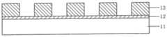
도1a 내지 도1d는 종래의 세미 애디티브 공법에 따른 인쇄회로기판 제조방법을 나타낸다.1A to 1D illustrate a method of manufacturing a printed circuit board according to a conventional semi-additive process.
도1a에서, 동박(12)과 보강기재(11)로 이루어진 동박적층판(CCL)의 동박(12) 표면에 도금 레지스트(13)를 도포하고 현상하여, 도금 레지스트 패턴을 형성한다.In FIG. 1A, a
통상적으로 사용되는 동박적층판의 동박(12)의 두께는 0.5㎛~3㎛ 정도이다. 도금 레지스트(13)로는 통상적으로 감광성의 드라이 필름이 사용된다.The thickness of the
도1b에서, 전해 도금을 통해 도금층(14)을 형성한다. 도금시 동박(12)은 시드 레이어(seed layer) 역할을 하게 된다. 그러나, 이때 도금에 의해 형성되는 도금층(14)의 두께는 도금시에 발생하는 편차로 인해 모든 면에 일정한 두께를 가질 수 없다.In Fig. 1B, the
도1c에서, 도금이 완료된 후 남아있는 도금 레지스트(13)를 박리해 준다.In Fig. 1C, the plating resist 13 remaining after the plating is completed is peeled off.
이 때, 도금 레지스트(13)를 박리할 때는 기판을 박리액에 담궈서 제거하게 되는데, 이때 도금 레지스트(13)가 완전히 제거되지 않고 도금층(14)의 측벽에 잔존물이 남는 문제점이 있다.In this case, when the plating resist 13 is peeled off, the substrate is immersed in a stripping solution to remove the plating resist. In this case, the plating resist 13 may not be completely removed, and a residue may remain on the sidewall of the
그리고 나서, 도1d에서, 동박(12) 중 회로 패턴이 되지 않는 부분을 소프트 에칭으로 제거하여 원하는 회로 패턴만을 남기면, 회로 패턴이 형성된다.Then, in FIG. 1D, if the portion of the
그러나 위와 같은 애디티브공법을사용한다 하더라도 여전히 원하는 두께를 얻을 수가 없다.However, even with the additive method described above, the desired thickness is still not obtained.
본 발명은 원재료로써 종래의 동박적층판을 사용하지 않는 인쇄회로기판 제조방법을 제공하는 것을 목적으로 한다.An object of the present invention is to provide a printed circuit board manufacturing method that does not use a conventional copper clad laminate as a raw material.
본 발명은 보다 박형의 인쇄회로기판을 제조할 수 있는 인쇄회로기판 제조방법을 제공하는 것을 목적으로 한다.An object of the present invention is to provide a printed circuit board manufacturing method that can produce a thinner printed circuit board.
본 발명에 따른 고밀도 인쇄회로기판은, 일정한 두께를 가지고 있는 제1 절연층; 및 상기 제1 절연층의 양측에 각각 뭍혀 있는 한쌍의 제1 회로층을 포함한다.A high density printed circuit board according to the present invention includes a first insulating layer having a predetermined thickness; And a pair of first circuit layers respectively laid on both sides of the first insulating layer.
또한, 본 발명에 따른 고밀도 인쇄회로기판의 제조방법은, 동호일이 일측에 형성되어 있는 한쌍의 케리어를 준비하는 제 1 단계; 상기 각각의 케리어의 동호일 위에 회로패턴을 가진 도금 레지스트를 형성한 후에 도금층을 형성하는 제 2 단계; 상기 도금 레지스트를 제거한 후에 상기 한쌍의 케리어의 사이에 접착제를 넣고 도금층이 서로 마주보록 하여 가접하는 제 3 단계; 상기 양측의 케리어를 제거한 후에 비아홀을 가공하고 시드층을 형성한 후에 비아홀의 부분만이 오픈되도록 도금 레지스트를 형성하는 제 4 단계; 및 도금 후에 도금 레지스트를 박리하며 에칭 공정을 통하여 시드층을 제거하는 제 5 단계를 포함하여 이루어진 것을 특징으로 한다.In addition, a method for manufacturing a high density printed circuit board according to the present invention includes a first step of preparing a pair of carriers having copper foils formed on one side; A second step of forming a plating layer after forming a plating resist having a circuit pattern on the copper foil of each carrier; A third step of removing the plating resist and inserting an adhesive between the pair of carriers and welding the plating layers to face each other; A fourth step of forming a plating resist such that only portions of the via holes are opened after processing the via holes after removing the carriers on both sides and forming a seed layer; And a fifth step of peeling the plating resist after plating and removing the seed layer through an etching process.
이하, 도면을 참조하여 본 발명을 보다 상세히 설명한다.Hereinafter, the present invention will be described in more detail with reference to the drawings.
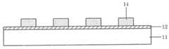
도 2는 본 발명의 일실시예에 따른 인쇄회로기판의 단면도이다.2 is a cross-sectional view of a printed circuit board according to an embodiment of the present invention.
도면을 참조하면, 본 발명의 일실시예에 따른 인쇄회로기판은 에폭시 수지층(21)에 회로패턴(22)이 파뭍혀 있음을 알 수 있다. 이에 따라 회로패턴(22)의 두께가 15~25㎛로서 기존기술과 비교하여 전체두께에서 약 30~50㎛까지 감소시킬 수가 있다. 또한 솔더 레지스트(24)의 두께 또한 도포전의 표면이 평탄하기 때문에 실장에 문제가 되지 않을 두께까지만 도포하는 것이 가능하기 때문에 두게 감소에 한 부문을 차지할 수 있다.Referring to the drawings, the printed circuit board according to an embodiment of the present invention can be seen that the
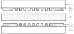
도3a 내지 도3g는 본 발명의 일 실시예에 따른 고밀도 인쇄회로기판의 제조 방법을 나타낸다. 도3a 내지 도3g를 참조하여 본 발명의 일 실시예에 따른 고밀도 인쇄회로기판의 제조 방법을 설명한다.3A to 3G illustrate a method of manufacturing a high density printed circuit board according to an embodiment of the present invention. A method of manufacturing a high density printed circuit board according to an embodiment of the present invention will be described with reference to FIGS. 3A to 3G.
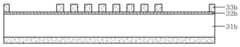
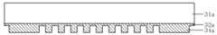
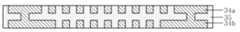
우선, 도3a에 도시된 바와 같은 얇은 동호일(32)이 케리어(31)에 붙어 있는 두개의 구조물로 공정을 시작한다.First, the process starts with two structures in which a
이때 사용되는 자재는 인쇄회로기판에 범용적으로 사용되는 재료를 적용한 다. 여기에서, 동호일(32)의 두께는 바람직하게 3㎛가 적절하다. 그리고, 케리어(31)의 두께는 15~100㎛가 적절하며, 그 재료는 동이나, 알루미늄등의 금속 메탈과 에폭시 등도 가능하다.In this case, the material used is a material commonly used for printed circuit boards. Here, the thickness of the
또한, 얇은 동호일(32)과 케리어(31)은 무기물 또는 유기물로 접합되어 있으며 고온고압의 공정 후에 쉽게 제거할 수 있다.In addition, the
이후에, 도 3b 및 도 3c에 도시된 바와 같이, 두개의 동호일(32)이 케리어(31)에 부착된 구조물의 각각의 양측에 에칭 레지스트(33a 또는 33b)를 적층하고 일면에 노광 현상 공정을 이용하여 에칭 레지스트(33a 또는 33b)에 회로패턴을 형성한다.Thereafter, as shown in FIGS. 3B and 3C, two copper foils 32 are laminated with etching resists 33a or 33b on each side of the structure attached to the
이러한 에칭 레지스트(33a, 33b)를 형성하는 방법은 사진법과 스크린 인쇄법으로 나눌수 있다. 그리고, 사진법은 드라이필름을 에칭 레지스트를 사용하는 D/F법과 액체 상태의 감광재를 사용하는 액상감광재법으로 구분된다.The method of forming the etching resists 33a and 33b can be divided into a photo method and a screen printing method. In addition, the photographing method is classified into a D / F method using an etching resist as a dry film and a liquid photosensitive material method using a liquid photosensitive material.
그리고, 도 3d 및 도 3e에 도시된 바와 같이, 동호일(32a, 32b)를 도금인입선으로 하여 전해 동도금을 수행하여 에칭 레지스트(33a, 또는 33b)에 동도금층 패턴(34a, 34b)을 형성한 후에 에칭 레지스트(33a, 33b)를 제거한다. 에칭 레지스트(33a, 33b)에 대한 동도금은 전해 동도금이 사용되며, 전해 동도금은 두꺼운 도금피막을 형성하기 쉽고, 막의 물성도 무전해 동도금에 비하여 우수하다.3D and 3E, the copper plating layers
다음에, 도 3f에 도시된 바와 같이 접착제(35)를 사이에 두고 동도금층 회로패턴(34a, 34b)가 형성된 2개의 기재를 고온, 고압의 공정을 거쳐 부착시킨다.Next, as shown in FIG. 3F, the two substrates on which the copper plating
이때, 동도금층 회로패턴(34a, 34b)의 표면에는 접착제(35)와의 접착력을 증 가시키기 위한 표면처리를 진행하며, 표면처리는 흑화처리 또는 브라운 흑화 처리 등이 바람직하다.At this time, the surface of the copper plating layer circuit pattern (34a, 34b) is subjected to a surface treatment for increasing the adhesive force with the adhesive 35, the surface treatment is preferably blackening treatment or brown blackening treatment.
접착제(35)로는 다층 인쇄회로기판 제조시에 층간 절연용으로서 열을 가할 때 적절한 접착력을 갖는 프리프렉을 사용하는 것이 바람직하다.As the adhesive 35, it is preferable to use a prepreg having an appropriate adhesive force when applying heat for interlayer insulation in the manufacture of a multilayer printed circuit board.
프리프렉은 유리섬유 소재에 접착제를 함침시킨 재질로서, 회로패턴이 형성된 회로층(34a, 34b)들 사이에 삽입되어 회로층들 사이의 절연역할을 함과 동시에 층들 사이의 접착층의 역할도 하게 된다.Prepreg is a material impregnated with glass fiber material and is inserted between the circuit layers 34a and 34b on which circuit patterns are formed, and serves as an insulating layer between the circuit layers, and also serves as an adhesive layer between the layers. .
접착제(35)를 도3f와 같이 배치한 후에 상하면에서 가열 가압하면 도3g와 같이 접착제(35)의 양면이 회로패턴(34a, 34b)으로 밀려들어가면서 회로패턴(34a, 34b)이 접착제(35)를 사이에 두고 부착된다.When the adhesive 35 is disposed as shown in FIG. 3F and heated and pressed from the upper and lower surfaces, both sides of the adhesive 35 are pushed into the
이후에, 도 3h에서 볼 수 있는 바와 같이 케리어(31a, 31b)를 제거해주는데 이때 손으로 제거가능하다.Thereafter, as shown in FIG. 3H, the
다음으로, 도 3i에 도시된 바와 같이 드릴 공정을 통하여 1층과 2층의 신호 연결을 위한 비아홀(36)을 형성한다.Next, as illustrated in FIG. 3I, a via
이 때의 드릴링 공정은 회로층(34a, 34b)와 접착제(35)를 드릴링하여야 하기 때문에 CNC 드릴을 이용한 기계적 드릴링이 바람직하다.Since the drilling process at this time must drill the circuit layers 34a and 34b and the adhesive 35, mechanical drilling using a CNC drill is preferable.
이후에, 도3j에서, 기판 전체를 무전해 동도금하여 약 1.0㎛~3.0㎛ 두께로 시드층(37)을 형성한다.Thereafter, in FIG. 3J, the entire substrate is electroless copper plated to form a
홀 내벽에 대한 동도금은 무전해 동도금과 전해 동도금의 순서로 진행된다. 이는 드릴링된 홀의 내벽이 절연체인 에폭시로 되어 있어 전기분해에 의한 전해 동 도금을 실시할 수 없기 때문이다. 따라서 무전해 동도금을 먼저 실시하고 이어서 전해 동도금을 실시하여 홀 내벽을 완전하게 동으로 도금한다.Copper plating on the inner wall of the hall proceeds in the order of electroless copper plating and electrolytic copper plating. This is because the inner wall of the drilled hole is made of epoxy, which is an insulator, so that electrolytic copper plating cannot be performed by electrolysis. Therefore, electroless copper plating is performed first, followed by electrolytic copper plating to completely plate the inner wall of the hole with copper.
무전해 도금은 수지, 세라믹, 유리 등과 같은 부도체의 표면에 도전성을 부여하기 위한 유일한 도금방법이다.Electroless plating is the only plating method for imparting conductivity to the surface of non-conductors such as resins, ceramics, glass, and the like.
무전해 동도금을 행하여 홀의 내벽에 도전성을 부여하였으므로 이제 전기분해를 이용한 전해 동도금이 가능하다. 이때, 비아부분만을 동도금하기 위해 도금 레지스트(38)을 비아부분을 제외한 부분에 형성한다. 즉, 도금 레지스트(38)을 도포한 후에 노광, 현상 공정을 통하여 비아부분만 오픈한다.Since electroless copper plating was performed to impart conductivity to the inner wall of the hole, electrolytic copper plating using electrolysis is now possible. At this time, in order to copper plate only the via portion, a plating resist 38 is formed on the portion except the via portion. That is, only the via portion is opened through the exposure and development processes after the plating resist 38 is applied.
이후, 전해동도금을 하여 비아부분만 도금을 하여 동도금층(39)를 형성하며, 이때 전해 동도금은 두꺼운 도금피막을 형성하기 쉽고, 막의 물성도 무전해 동도금에 비하여 우수하다.Subsequently, only the via part is plated by electrolytic copper plating to form a copper plating layer 39. In this case, the electrolytic copper plating is easy to form a thick plating film, and the properties of the film are also superior to electroless copper plating.
동도금층(39)이 비아홀(36)의 내벽을 도금하면서 비아홀(36)의 내부를 충진하게 된다.The copper plating layer 39 fills the inside of the via
다음에, 도3k에 도시된 바와 같이, 동도금층(39)을 형성한 후에 도금 레지스트(38)를 제거하여 시드층(37)이 드러나도록 한다.Next, as shown in FIG. 3K, after forming the copper plating layer 39, the plating resist 38 is removed so that the
그리고, 도 3l에 도시된 바와 같이 에칭 공정을 통하여 표면의 시드층(37)과 동호일(32)를 제거한다. 이때, 에칭 공정을 진행하여 접착제(35)가 드러날 때까지 에칭을 진행한다.As shown in FIG. 3L, the
즉, 도금후에 표면에칭을 통하여 시드층(37)과 동호일(32a,32b)의 표면을 에칭하여 접착제(35)의 패턴이 외부에 노출되도록 한다. 이와 같은 공정을 통해, 이 후에 4층 인쇄회로기판을 형성할 때 1층 및 2층 회로패턴이 상하면에 형성되어 있는 중심층이 형성된다.That is, after plating, the surface of the
물론, 도 3m에 도시된 바와 같이 솔더 레지스트(40)을 도포하고, 노광 현상을 통하여 표면처리(금도금 또는 OSP 처리 등)가 될 부분을 형성한 후에 표면처리를 진행하여 중간 매개체(interposer) 제작을 완료한다.Of course, as shown in FIG. 3m, the solder resist 40 is applied, and after forming a portion to be a surface treatment (gold plating or OSP treatment) through an exposure phenomenon, the surface treatment is performed to produce an intermediate interposer. To complete.
도 4a 내지 도 4h는 본 발명이 일실시예에 따른 고밀도 기판의 제조방법에서 레이저 드릴을 사용하여 비아를 형성하는 과정을 나타내는 공정도로서, 도 3d의 단계 이후부터 도시하면서 설명하며 도 3d 이전의 단계는 동일하다..4A to 4H are process diagrams illustrating a process of forming a via using a laser drill in the method of manufacturing a high density substrate according to an embodiment of the present invention. Is the same.
먼저, 도 4a를 참조하면, 두개의 회로층(44a, 44b)중에서 상부 회로층(44a)의 비아가 형성될 부분은 애널링 링(40) 형상을 만든다.First, referring to FIG. 4A, a portion of the two
그리고, 접착제(45)를 사이에 두고 상부 회로층(44a)의 비아가 형성될 부분에 애널링 링(40)이 형성된 동도금층 회로패턴(44a, 44b)가 형성된 2개의 기재를 고온, 고압의 공정을 거쳐 부착시킨다.The two substrates on which the copper plating
이때, 동도금층 회로패턴(44a, 44b)의 표면에는 접착제(45)와의 접착력을 증가시키기 위한 표면처리를 진행하며, 표면처리는 흑화처리 또는 브라운 흑화 처리 등이 바람직하다.At this time, the surface of the copper plating layer circuit pattern (44a, 44b) is subjected to a surface treatment for increasing the adhesive force with the adhesive 45, the surface treatment is preferably blackening treatment or brown blackening treatment.
접착제(45)로는 다층 인쇄회로기판 제조시에 층간 절연용으로서 열을 가할 때 적절한 접착력을 갖는 프리프렉을 사용하는 것이 바람직하다.As the adhesive 45, it is preferable to use a prepreg having an appropriate adhesive force when applying heat for interlayer insulation in the manufacture of a multilayer printed circuit board.
접착제(45)를 도4a와 같이 배치한 후에 상하면에서 가열 가압하면 접착제(45)의 양면이 회로패턴(44a, 44b)으로 밀려들어가면서 회로패턴(44a, 44b)이 접착 제(45)를 사이에 두고 부착된다.After arranging the adhesive 45 as shown in FIG. 4A and heating and pressing it from the upper and lower surfaces, both surfaces of the adhesive 45 are pushed into the
이후에, 도 4b에서 볼 수 있는 바와 같이 케리어(41a, 41b)를 제거해주는데 이때 손으로 제거가능하다.Thereafter, as shown in FIG. 4B, the
다음에, 도 4c에 도시된 바와 같이 케리어(41a, 41b)를 제거한 후에 시드층(42a, 42b)을 에칭공정을 통하여 제거해준다.Next, as shown in FIG. 4C, the carrier layers 41a and 41b are removed, and then the seed layers 42a and 42b are removed through an etching process.
다음으로, 도 4d에 도시된 바와 같이 레이저 드릴 공정을 통하여 1층과 2층의 신호 연결을 위한 비아홀(46)을 형성한다. 이때, 레이저 드릴을 사용하는 것은 하부 동도금층(44b)에 영향을 주지 않기 위해서이다. 그리고, 이미 상부 회로층(44a)에 애널링 링(40)이 형성되어 비아(46)가 형성될 부분에 동도금층(44a)가 제거되어 있음으로 동도금층(44a)를 제거할 공정이 필요하지 않다.Next, as shown in FIG. 4D, a via
이후에, 도 4e에 도시된 바와 같이 비아(46)이 형성된 기판 전체를 무전해 동도금하여 약 1.0㎛~3.0㎛ 두께로 시드층(47)을 형성한다.Thereafter, as shown in FIG. 4E, the entire substrate on which the
홀 내벽에 대한 동도금은 무전해 동도금과 전해 동도금의 순서로 진행된다. 이는 드릴링된 홀의 내벽이 절연체인 에폭시로 되어 있어 전기분해에 의한 전해 동도금을 실시할 수 없기 때문이다. 따라서 무전해 동도금을 먼저 실시하고 이어서 전해 동도금을 실시하여 홀 내벽을 완전하게 동으로 도금한다.Copper plating on the inner wall of the hall proceeds in the order of electroless copper plating and electrolytic copper plating. This is because the inner wall of the drilled hole is made of epoxy, which is an insulator, so that electrolytic copper plating cannot be performed by electrolysis. Therefore, electroless copper plating is performed first, followed by electrolytic copper plating to completely plate the inner wall of the hole with copper.
이때, 비아부분만을 동도금하기 위해 도금 레지스트(48)을 비아부분을 제외한 부분에 형성한다. 즉, 도금 레지스트(48)을 도포한 후에 노광, 현상 공정을 통하여 비아부분만 오픈한다.At this time, in order to copper plate only the via portion, a plating resist 48 is formed on the portion except the via portion. That is, only the via portion is opened through the exposure and development processes after the plating resist 48 is applied.
이후, 도 4f에 도시된 바와 같이 전해동도금을 하여 비아부분만 도금을 하여 동도금층(49)를 형성하며, 이때 전해 동도금은 두꺼운 도금피막을 형성하기 쉽고, 막의 물성도 무전해 동도금에 비하여 우수하다.Thereafter, as shown in FIG. 4F, only the via part is plated to form a
동도금층(49)이 비아홀(46)의 내벽을 도금하면서 비아홀(46)의 내부를 충진하게 된다.The
다음에, 도4g에 도시된 바와 같이, 동도금층(49)을 형성한 후에 도금 레지스트(48)를 제거하여 시드층(47)이 드러나도록 한다.Next, as shown in Fig. 4G, after forming the
그리고, 에칭 공정을 통하여 표면의 시드층(47)과 동호일(42)를 제거한다. 이때, 에칭 공정을 진행하여 접착제(45)가 드러날 때까지 에칭을 진행한다.Then, the
즉, 도금후에 표면에칭을 통하여 시드층(47)과 동호일(42a,42b)의 표면을 에칭하여 접착제(45)의 패턴이 외부에 노출되도록 한다. 이와 같은 공정을 통해, 이후에 4층 인쇄회로기판을 형성할 때 1층 및 2층 회로패턴이 상하면에 형성되어 있는 중심층이 형성된다.That is, after plating, the surface of the
물론, 도 4h에 도시된 바와 같이 솔더 레지스트(50)을 도포하고, 노광 현상을 통하여 표면처리(금도금 또는 OSP 처리 등)가 될 부분을 형성한 후에 표면처리를 진행하여 중간 매개체(interposer) 제작을 완료한다.Of course, as shown in FIG. 4H, the solder resist 50 is applied, and after forming a portion to be a surface treatment (gold plating or OSP treatment) through an exposure phenomenon, the surface treatment is performed to produce an intermediate interposer. To complete.
상기와 같은 본 발명에 따르면, 중간 매개체의 전체 두께에서 60um~110um 정도의 두께를 감소시킬 수 있는 효과가 있다.According to the present invention as described above, there is an effect that can reduce the thickness of about 60um ~ 110um in the total thickness of the intermediate medium.
또한, 본 발명에 따르면, 시드층을 사용하여 회로를 형성하기 때문에 미세 패턴이 되는데 이때에 회로의 밀착력이 증가하며, 이후에 공정 진행시에 밀착력 부족에 의한 불량발생이 없으며, 단선불량도 없다.In addition, according to the present invention, since a circuit is formed using the seed layer, a fine pattern is formed. At this time, the adhesion of the circuit increases, and thereafter, no defect occurs due to the lack of adhesion during the process, and there is no disconnection defect.
또한, 본 발명에 따르면, 시드층을 제거해주기 때문에 제거된 부분이 평탄도의 기준이 되어 패턴의 평탄도가 기존공정보다 좋다.In addition, according to the present invention, since the seed layer is removed, the removed portion serves as a criterion of the flatness, and the flatness of the pattern is better than that of the existing process.
이상 본 발명을 실시예를 참조하여 설명하였으나, 이상의 설명한 실시예들은 하나의 예시로서, 본 발명의 범위는 이하의 특허청구범위에 의해 정해지고, 당업자들은 본 발명의 범위에 속하는 범위 내에서 위 실시예 들에 다양한 변형을 가할 수 있음을 이해할 것이며, 이들은 모두 본 발명의 범위에 포함된다.Although the present invention has been described above with reference to the embodiments, the above-described embodiments are exemplified as an example, and the scope of the present invention is defined by the following claims, and those skilled in the art can implement the above within the scope of the present invention. It will be understood that various modifications may be made to the examples, all of which are included in the scope of the present invention.
Claims (10)
Translated fromKoreanPriority Applications (6)
| Application Number | Priority Date | Filing Date | Title |
|---|---|---|---|
| KR1020050110805AKR100733253B1 (en) | 2005-11-18 | 2005-11-18 | High density printed circuit board and manufacturing method thereof |
| DE102006051762ADE102006051762B4 (en) | 2005-11-18 | 2006-11-02 | High-density printed circuit board and method for its production |
| JP2006305080AJP2007142403A (en) | 2005-11-18 | 2006-11-10 | Printed board and manufacturing method of same |
| US11/599,435US20070114203A1 (en) | 2005-11-18 | 2006-11-15 | High density printed circuit board and method of manufacturing the same |
| CNA2006101452054ACN1968565A (en) | 2005-11-18 | 2006-11-17 | High density printed circuit board and method of manufacturing the same |
| US12/314,783US8256112B2 (en) | 2005-11-18 | 2008-12-16 | Method of manufacturing high density printed circuit board |
Applications Claiming Priority (1)
| Application Number | Priority Date | Filing Date | Title |
|---|---|---|---|
| KR1020050110805AKR100733253B1 (en) | 2005-11-18 | 2005-11-18 | High density printed circuit board and manufacturing method thereof |
Publications (2)
| Publication Number | Publication Date |
|---|---|
| KR20070052965A KR20070052965A (en) | 2007-05-23 |
| KR100733253B1true KR100733253B1 (en) | 2007-06-27 |
Family
ID=38047787
Family Applications (1)
| Application Number | Title | Priority Date | Filing Date |
|---|---|---|---|
| KR1020050110805AExpired - Fee RelatedKR100733253B1 (en) | 2005-11-18 | 2005-11-18 | High density printed circuit board and manufacturing method thereof |
Country Status (5)
| Country | Link |
|---|---|
| US (2) | US20070114203A1 (en) |
| JP (1) | JP2007142403A (en) |
| KR (1) | KR100733253B1 (en) |
| CN (1) | CN1968565A (en) |
| DE (1) | DE102006051762B4 (en) |
Cited By (2)
| Publication number | Priority date | Publication date | Assignee | Title |
|---|---|---|---|---|
| KR101006603B1 (en) | 2009-01-09 | 2011-01-07 | 삼성전기주식회사 | Printed circuit board and manufacturing method thereof |
| WO2019107819A1 (en)* | 2017-11-29 | 2019-06-06 | (주)잉크테크 | Method for manufacturing printed circuit board |
Families Citing this family (28)
| Publication number | Priority date | Publication date | Assignee | Title |
|---|---|---|---|---|
| US6930256B1 (en) | 2002-05-01 | 2005-08-16 | Amkor Technology, Inc. | Integrated circuit substrate having laser-embedded conductive patterns and method therefor |
| US7548430B1 (en) | 2002-05-01 | 2009-06-16 | Amkor Technology, Inc. | Buildup dielectric and metallization process and semiconductor package |
| US9691635B1 (en) | 2002-05-01 | 2017-06-27 | Amkor Technology, Inc. | Buildup dielectric layer having metallization pattern semiconductor package fabrication method |
| US7670962B2 (en)* | 2002-05-01 | 2010-03-02 | Amkor Technology, Inc. | Substrate having stiffener fabrication method |
| US11081370B2 (en) | 2004-03-23 | 2021-08-03 | Amkor Technology Singapore Holding Pte. Ltd. | Methods of manufacturing an encapsulated semiconductor device |
| US10811277B2 (en) | 2004-03-23 | 2020-10-20 | Amkor Technology, Inc. | Encapsulated semiconductor package |
| US8826531B1 (en) | 2005-04-05 | 2014-09-09 | Amkor Technology, Inc. | Method for making an integrated circuit substrate having laminated laser-embedded circuit layers |
| US7589398B1 (en) | 2006-10-04 | 2009-09-15 | Amkor Technology, Inc. | Embedded metal features structure |
| CN101022189A (en)* | 2006-12-30 | 2007-08-22 | 番禺得意精密电子工业有限公司 | Electric connector |
| US7752752B1 (en) | 2007-01-09 | 2010-07-13 | Amkor Technology, Inc. | Method of fabricating an embedded circuit pattern |
| US7874065B2 (en)* | 2007-10-31 | 2011-01-25 | Nguyen Vinh T | Process for making a multilayer circuit board |
| KR100890447B1 (en)* | 2007-12-27 | 2009-03-26 | 주식회사 코리아써키트 | Embedded printed circuit board manufacturing method |
| JP5138459B2 (en)* | 2008-05-15 | 2013-02-06 | 新光電気工業株式会社 | Wiring board manufacturing method |
| TWI430722B (en) | 2008-09-05 | 2014-03-11 | Unimicron Technology Corp | Circuit structure of circuit board and process thereof |
| CN102265714B (en)* | 2008-12-22 | 2014-05-14 | 富士通株式会社 | Electronic component and method for manufacturing same |
| US8872329B1 (en) | 2009-01-09 | 2014-10-28 | Amkor Technology, Inc. | Extended landing pad substrate package structure and method |
| TWI384925B (en)* | 2009-03-17 | 2013-02-01 | Advanced Semiconductor Eng | Structure of embedded-trace substrate and method of manufacturing the same |
| TWI393508B (en)* | 2009-12-17 | 2013-04-11 | Unimicron Technology Corp | Circuit board and process for fabricating the same |
| KR101140982B1 (en)* | 2010-09-07 | 2012-05-03 | 삼성전기주식회사 | Single layer printed circuit board and manufacturing method thereof |
| CN103140050B (en)* | 2011-12-05 | 2015-07-15 | 深南电路有限公司 | Machining method of burying capacitance circuit board |
| US8502391B2 (en) | 2011-12-08 | 2013-08-06 | Stats Chippac, Ltd. | Semiconductor device and method of making single layer substrate with asymmetrical fibers and reduced warpage |
| KR20130141927A (en)* | 2012-06-18 | 2013-12-27 | 삼성전기주식회사 | Printed circuit board and method of manufacturing for printed circuit board |
| US9876992B2 (en)* | 2014-04-30 | 2018-01-23 | Panasonic Intellectual Property Management Co., Ltd. | Imaging apparatus and distance measuring apparatus using the same |
| KR102497595B1 (en) | 2016-01-05 | 2023-02-08 | 삼성전자주식회사 | Package substrate, methods for fabricating the same and package device including the package substrate |
| CN107949173B (en)* | 2017-11-22 | 2019-10-08 | 广州兴森快捷电路科技有限公司 | The boring method of wiring board |
| CN110600458A (en)* | 2018-06-12 | 2019-12-20 | 深圳市环基实业有限公司 | LED lamp and manufacturing method thereof |
| CN110863224B (en)* | 2019-11-22 | 2022-09-30 | 中国船舶重工集团公司第十二研究所 | Non-ferrous metal part micro-arc oxidation protective agent and local protection method |
| CN111629527B (en)* | 2020-06-12 | 2023-07-04 | 东莞市龙谊电子科技有限公司 | Manufacturing method of flexible circuit board and flexible circuit board thereof |
Citations (1)
| Publication number | Priority date | Publication date | Assignee | Title |
|---|---|---|---|---|
| KR20050049452A (en)* | 1999-08-25 | 2005-05-25 | 히다치 가세고교 가부시끼가이샤 | Adhesive agent, method for connecting wiring terminals and wiring structure |
Family Cites Families (18)
| Publication number | Priority date | Publication date | Assignee | Title |
|---|---|---|---|---|
| US3161945A (en)* | 1958-05-21 | 1964-12-22 | Rogers Corp | Method of making a printed circuit |
| US4354895A (en)* | 1981-11-27 | 1982-10-19 | International Business Machines Corporation | Method for making laminated multilayer circuit boards |
| CA1283591C (en)* | 1985-08-26 | 1991-04-30 | Theron L. Ellis | Method for making a flush surface laminate for a multilayer circuit board |
| JP2739726B2 (en)* | 1990-09-27 | 1998-04-15 | インターナシヨナル・ビジネス・マシーンズ・コーポレーシヨン | Multilayer printed circuit board |
| IL111497A (en)* | 1993-12-08 | 2001-01-28 | Rohco Inc Mcgean | Silane compositions useful as adhesives |
| JP3149352B2 (en)* | 1996-02-29 | 2001-03-26 | インターナショナル・ビジネス・マシーンズ・コーポレ−ション | Method of forming conductor layer of substrate |
| EP1250033B1 (en)* | 1996-12-26 | 2004-09-08 | Matsushita Electric Industrial Co., Ltd. | Printed circuit board and electronic component |
| JPH11121897A (en)* | 1997-10-14 | 1999-04-30 | Fujitsu Ltd | Method of manufacturing printed wiring board mounting a plurality of circuit elements on board and structure of printed wiring board |
| DE19910482A1 (en)* | 1999-03-10 | 2000-05-04 | Stp Elektronische Systeme Gmbh | Wiring level production on a support, especially for multilayer circuit board production, involves leaving an exposed and developed photosensitive resin layer as insulation between conductive regions |
| US6198166B1 (en)* | 1999-07-01 | 2001-03-06 | Intersil Corporation | Power semiconductor mounting package containing ball grid array |
| US6711813B1 (en)* | 1999-11-05 | 2004-03-30 | Interuniversitair Microelektronica Centrum | Method for fabricating a thin film build-up structure on a sequentially laminated printed circuit board base |
| JP3585796B2 (en)* | 1999-12-17 | 2004-11-04 | 新光電気工業株式会社 | Multilayer wiring board manufacturing method and semiconductor device |
| US6522018B1 (en)* | 2000-05-16 | 2003-02-18 | Micron Technology, Inc. | Ball grid array chip packages having improved testing and stacking characteristics |
| JP3729092B2 (en)* | 2001-06-19 | 2005-12-21 | ソニー株式会社 | Conductive bonding material, multilayer printed wiring board, and method for manufacturing multilayer printed wiring board |
| KR100671541B1 (en)* | 2001-06-21 | 2007-01-18 | (주)글로벌써키트 | Manufacturing method of impregnated printed circuit board |
| JP2003163458A (en)* | 2001-11-29 | 2003-06-06 | Fujitsu Ltd | Multilayer wiring board and manufacturing method thereof |
| US20030197514A1 (en)* | 2002-04-22 | 2003-10-23 | Howard Hsu | System and method for testing a printed circuit board by employing a ceramic substrate with micro-probes formed on the ceramic substrate |
| US20060043603A1 (en)* | 2004-08-31 | 2006-03-02 | Lsi Logic Corporation | Low temperature PB-free processing for semiconductor devices |
- 2005
- 2005-11-18KRKR1020050110805Apatent/KR100733253B1/ennot_activeExpired - Fee Related
- 2006
- 2006-11-02DEDE102006051762Apatent/DE102006051762B4/ennot_activeExpired - Fee Related
- 2006-11-10JPJP2006305080Apatent/JP2007142403A/enactivePending
- 2006-11-15USUS11/599,435patent/US20070114203A1/ennot_activeAbandoned
- 2006-11-17CNCNA2006101452054Apatent/CN1968565A/enactivePending
- 2008
- 2008-12-16USUS12/314,783patent/US8256112B2/ennot_activeExpired - Fee Related
Patent Citations (1)
| Publication number | Priority date | Publication date | Assignee | Title |
|---|---|---|---|---|
| KR20050049452A (en)* | 1999-08-25 | 2005-05-25 | 히다치 가세고교 가부시끼가이샤 | Adhesive agent, method for connecting wiring terminals and wiring structure |
Cited By (2)
| Publication number | Priority date | Publication date | Assignee | Title |
|---|---|---|---|---|
| KR101006603B1 (en) | 2009-01-09 | 2011-01-07 | 삼성전기주식회사 | Printed circuit board and manufacturing method thereof |
| WO2019107819A1 (en)* | 2017-11-29 | 2019-06-06 | (주)잉크테크 | Method for manufacturing printed circuit board |
Also Published As
| Publication number | Publication date |
|---|---|
| DE102006051762A1 (en) | 2007-06-06 |
| US20070114203A1 (en) | 2007-05-24 |
| US8256112B2 (en) | 2012-09-04 |
| CN1968565A (en) | 2007-05-23 |
| US20090101510A1 (en) | 2009-04-23 |
| KR20070052965A (en) | 2007-05-23 |
| JP2007142403A (en) | 2007-06-07 |
| DE102006051762B4 (en) | 2013-03-07 |
Similar Documents
| Publication | Publication Date | Title |
|---|---|---|
| KR100733253B1 (en) | High density printed circuit board and manufacturing method thereof | |
| KR100867148B1 (en) | Printed Circuit Board and Manufacturing Method | |
| JP5101542B2 (en) | Chip built-in printed circuit board and manufacturing method thereof | |
| KR101015704B1 (en) | Chip embedded printed circuit board and its manufacturing method | |
| US8236690B2 (en) | Method for fabricating semiconductor package substrate having different thicknesses between wire bonding pad and ball pad | |
| US20060180346A1 (en) | High aspect ratio plated through holes in a printed circuit board | |
| KR100619348B1 (en) | Manufacturing Method of Package Substrate Using Electroless Nickel Plating | |
| KR100965341B1 (en) | Manufacturing method of printed circuit board | |
| CN106879188B (en) | A kind of production method and circuit board of built-in component type circuit board | |
| KR20040075595A (en) | Method for manufacturing double side a flexible printed circuit board | |
| KR100861620B1 (en) | Manufacturing method of printed circuit board | |
| KR20010009975A (en) | Method of producing a multi-layer printed-circuit board | |
| KR100752017B1 (en) | Manufacturing method of printed circuit board | |
| KR100783462B1 (en) | Electronic element embedded printed circuit board and its manufacturing method | |
| KR100704920B1 (en) | Printed circuit board and manufacturing method using bump board | |
| KR100771320B1 (en) | Chip embedded printed circuit board and its manufacturing method | |
| KR20060042723A (en) | Manufacturing method of flexible multilayer printed circuit board | |
| KR100894180B1 (en) | Printed Circuit Board Manufacturing Method | |
| KR101081153B1 (en) | Method for fabricating printed-circuit-board including embedded fine pattern | |
| KR100658437B1 (en) | Printed circuit board and manufacturing method using bump board | |
| KR20150094154A (en) | Embedded board and method of manufacturing the same | |
| KR101436827B1 (en) | Printed circuit board and manufacturing method thereof | |
| KR101085576B1 (en) | Method for manufacturing printed circuit board using metal and printed circuit board manufactured using same | |
| JP4736251B2 (en) | Film carrier and manufacturing method thereof | |
| KR100566912B1 (en) | Method of manufacturing flexible printed circuit board with partial copper plating |
Legal Events
| Date | Code | Title | Description |
|---|---|---|---|
| A201 | Request for examination | ||
| PA0109 | Patent application | St.27 status event code:A-0-1-A10-A12-nap-PA0109 | |
| PA0201 | Request for examination | St.27 status event code:A-1-2-D10-D11-exm-PA0201 | |
| E902 | Notification of reason for refusal | ||
| PE0902 | Notice of grounds for rejection | St.27 status event code:A-1-2-D10-D21-exm-PE0902 | |
| P11-X000 | Amendment of application requested | St.27 status event code:A-2-2-P10-P11-nap-X000 | |
| P13-X000 | Application amended | St.27 status event code:A-2-2-P10-P13-nap-X000 | |
| E90F | Notification of reason for final refusal | ||
| PE0902 | Notice of grounds for rejection | St.27 status event code:A-1-2-D10-D21-exm-PE0902 | |
| R18-X000 | Changes to party contact information recorded | St.27 status event code:A-3-3-R10-R18-oth-X000 | |
| PG1501 | Laying open of application | St.27 status event code:A-1-1-Q10-Q12-nap-PG1501 | |
| E701 | Decision to grant or registration of patent right | ||
| PE0701 | Decision of registration | St.27 status event code:A-1-2-D10-D22-exm-PE0701 | |
| GRNT | Written decision to grant | ||
| PR0701 | Registration of establishment | St.27 status event code:A-2-4-F10-F11-exm-PR0701 | |
| PR1002 | Payment of registration fee | St.27 status event code:A-2-2-U10-U11-oth-PR1002 Fee payment year number:1 | |
| PG1601 | Publication of registration | St.27 status event code:A-4-4-Q10-Q13-nap-PG1601 | |
| PR1001 | Payment of annual fee | St.27 status event code:A-4-4-U10-U11-oth-PR1001 Fee payment year number:4 | |
| PR1001 | Payment of annual fee | St.27 status event code:A-4-4-U10-U11-oth-PR1001 Fee payment year number:5 | |
| PR1001 | Payment of annual fee | St.27 status event code:A-4-4-U10-U11-oth-PR1001 Fee payment year number:6 | |
| FPAY | Annual fee payment | Payment date:20130403 Year of fee payment:7 | |
| PR1001 | Payment of annual fee | St.27 status event code:A-4-4-U10-U11-oth-PR1001 Fee payment year number:7 | |
| FPAY | Annual fee payment | Payment date:20140325 Year of fee payment:8 | |
| PR1001 | Payment of annual fee | St.27 status event code:A-4-4-U10-U11-oth-PR1001 Fee payment year number:8 | |
| R18-X000 | Changes to party contact information recorded | St.27 status event code:A-5-5-R10-R18-oth-X000 | |
| PR1001 | Payment of annual fee | St.27 status event code:A-4-4-U10-U11-oth-PR1001 Fee payment year number:9 | |
| PR1001 | Payment of annual fee | St.27 status event code:A-4-4-U10-U11-oth-PR1001 Fee payment year number:10 | |
| LAPS | Lapse due to unpaid annual fee | ||
| PC1903 | Unpaid annual fee | St.27 status event code:A-4-4-U10-U13-oth-PC1903 Not in force date:20170622 Payment event data comment text:Termination Category : DEFAULT_OF_REGISTRATION_FEE | |
| PC1903 | Unpaid annual fee | St.27 status event code:N-4-6-H10-H13-oth-PC1903 Ip right cessation event data comment text:Termination Category : DEFAULT_OF_REGISTRATION_FEE Not in force date:20170622 | |
| R18-X000 | Changes to party contact information recorded | St.27 status event code:A-5-5-R10-R18-oth-X000 |