KR100732849B1 - Organic light emitting display - Google Patents
Organic light emitting displayDownload PDFInfo
- Publication number
- KR100732849B1 KR100732849B1KR1020050127223AKR20050127223AKR100732849B1KR 100732849 B1KR100732849 B1KR 100732849B1KR 1020050127223 AKR1020050127223 AKR 1020050127223AKR 20050127223 AKR20050127223 AKR 20050127223AKR 100732849 B1KR100732849 B1KR 100732849B1
- Authority
- KR
- South Korea
- Prior art keywords
- transparent
- light emitting
- organic light
- layer
- electrode
- Prior art date
- Legal status (The legal status is an assumption and is not a legal conclusion. Google has not performed a legal analysis and makes no representation as to the accuracy of the status listed.)
- Active
Links
- 230000000903blocking effectEffects0.000claimsabstractdescription25
- 239000000758substrateSubstances0.000claimsabstractdescription17
- 239000010409thin filmSubstances0.000claimsabstractdescription16
- 239000010408filmSubstances0.000claimsabstractdescription14
- 239000004065semiconductorSubstances0.000claimsdescription12
- 239000000463materialSubstances0.000claimsdescription8
- 239000004983Polymer Dispersed Liquid CrystalSubstances0.000claimsdescription5
- 229910002704AlGaNInorganic materials0.000claimsdescription2
- 229910007717ZnSnOInorganic materials0.000claimsdescription2
- 229910003460diamondInorganic materials0.000claimsdescription2
- 239000010432diamondSubstances0.000claimsdescription2
- AMGQUBHHOARCQH-UHFFFAOYSA-Nindium;oxotinChemical compound[In].[Sn]=OAMGQUBHHOARCQH-UHFFFAOYSA-N0.000claimsdescription2
- 150000004767nitridesChemical class0.000claimsdescription2
- YVTHLONGBIQYBO-UHFFFAOYSA-Nzinc indium(3+) oxygen(2-)Chemical compound[O--].[Zn++].[In+3]YVTHLONGBIQYBO-UHFFFAOYSA-N0.000claimsdescription2
- TYHJXGDMRRJCRY-UHFFFAOYSA-Nzinc indium(3+) oxygen(2-) tin(4+)Chemical compound[O-2].[Zn+2].[Sn+4].[In+3]TYHJXGDMRRJCRY-UHFFFAOYSA-N0.000claimsdescription2
- 239000010410layerSubstances0.000description66
- 239000011229interlayerSubstances0.000description7
- 239000004973liquid crystal related substanceSubstances0.000description5
- 239000012780transparent materialSubstances0.000description3
- 230000005540biological transmissionEffects0.000description1
- 239000011521glassSubstances0.000description1
- 230000001788irregularEffects0.000description1
- 238000004519manufacturing processMethods0.000description1
- 238000012986modificationMethods0.000description1
- 230000004048modificationEffects0.000description1
- 230000003287optical effectEffects0.000description1
- 208000017983photosensitivity diseaseDiseases0.000description1
- 231100000434photosensitizationToxicity0.000description1
- 239000004033plasticSubstances0.000description1
- 229910052594sapphireInorganic materials0.000description1
- 239000010980sapphireSubstances0.000description1
Images

Classifications
- H—ELECTRICITY
- H05—ELECTRIC TECHNIQUES NOT OTHERWISE PROVIDED FOR
- H05B—ELECTRIC HEATING; ELECTRIC LIGHT SOURCES NOT OTHERWISE PROVIDED FOR; CIRCUIT ARRANGEMENTS FOR ELECTRIC LIGHT SOURCES, IN GENERAL
- H05B33/00—Electroluminescent light sources
- H05B33/12—Light sources with substantially two-dimensional radiating surfaces
- H05B33/22—Light sources with substantially two-dimensional radiating surfaces characterised by the chemical or physical composition or the arrangement of auxiliary dielectric or reflective layers
- H—ELECTRICITY
- H10—SEMICONDUCTOR DEVICES; ELECTRIC SOLID-STATE DEVICES NOT OTHERWISE PROVIDED FOR
- H10K—ORGANIC ELECTRIC SOLID-STATE DEVICES
- H10K59/00—Integrated devices, or assemblies of multiple devices, comprising at least one organic light-emitting element covered by group H10K50/00
- H10K59/50—OLEDs integrated with light modulating elements, e.g. with electrochromic elements, photochromic elements or liquid crystal elements
- H—ELECTRICITY
- H10—SEMICONDUCTOR DEVICES; ELECTRIC SOLID-STATE DEVICES NOT OTHERWISE PROVIDED FOR
- H10K—ORGANIC ELECTRIC SOLID-STATE DEVICES
- H10K59/00—Integrated devices, or assemblies of multiple devices, comprising at least one organic light-emitting element covered by group H10K50/00
- H10K59/10—OLED displays
- H10K59/12—Active-matrix OLED [AMOLED] displays
- H10K59/128—Active-matrix OLED [AMOLED] displays comprising two independent displays, e.g. for emitting information from two major sides of the display
- G—PHYSICS
- G02—OPTICS
- G02F—OPTICAL DEVICES OR ARRANGEMENTS FOR THE CONTROL OF LIGHT BY MODIFICATION OF THE OPTICAL PROPERTIES OF THE MEDIA OF THE ELEMENTS INVOLVED THEREIN; NON-LINEAR OPTICS; FREQUENCY-CHANGING OF LIGHT; OPTICAL LOGIC ELEMENTS; OPTICAL ANALOGUE/DIGITAL CONVERTERS
- G02F2201/00—Constructional arrangements not provided for in groups G02F1/00 - G02F7/00
- G02F2201/44—Arrangements combining different electro-active layers, e.g. electrochromic, liquid crystal or electroluminescent layers
- H—ELECTRICITY
- H10—SEMICONDUCTOR DEVICES; ELECTRIC SOLID-STATE DEVICES NOT OTHERWISE PROVIDED FOR
- H10K—ORGANIC ELECTRIC SOLID-STATE DEVICES
- H10K2102/00—Constructional details relating to the organic devices covered by this subclass
- H10K2102/301—Details of OLEDs
- H10K2102/302—Details of OLEDs of OLED structures
- H10K2102/3023—Direction of light emission
- H10K2102/3031—Two-side emission, e.g. transparent OLEDs [TOLED]
- H—ELECTRICITY
- H10—SEMICONDUCTOR DEVICES; ELECTRIC SOLID-STATE DEVICES NOT OTHERWISE PROVIDED FOR
- H10K—ORGANIC ELECTRIC SOLID-STATE DEVICES
- H10K59/00—Integrated devices, or assemblies of multiple devices, comprising at least one organic light-emitting element covered by group H10K50/00
- H10K59/10—OLED displays
- H10K59/12—Active-matrix OLED [AMOLED] displays
- H10K59/126—Shielding, e.g. light-blocking means over the TFTs
Landscapes
- Engineering & Computer Science (AREA)
- Microelectronics & Electronic Packaging (AREA)
- Electroluminescent Light Sources (AREA)
- Devices For Indicating Variable Information By Combining Individual Elements (AREA)
- Control Of Indicators Other Than Cathode Ray Tubes (AREA)
- Liquid Crystal (AREA)
- Thin Film Transistor (AREA)
Abstract
Translated fromKoreanDescription
Translated fromKorean도 1은 종래 유기 발광 표시장치를 나타낸 도이다.1 illustrates a conventional organic light emitting display device.
도 2는 본 발명에 따른 유기 발광 표시장치의 일례를 나타낸 도이다.2 illustrates an example of an organic light emitting diode display according to the present invention.
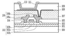
*** 도면의 주요 부호에 대한 설명 ****** Description of the main symbols in the drawings ***
200: 표시부301: 제 1 투명 전극200: display unit 301: first transparent electrode
302: 광차단막 303: 제 2 투명 전극302: light blocking film 303: second transparent electrode
본 발명은 유기 발광 표시장치에 관한 것으로 더욱 상세하게는, 투명 양면 발광 다이오드와 빛을 차단하는 광차단막을 구비하여 사용자가 원하는 시점에서 화상을 자유롭게 표시하기 위한 유기 발광 표시장치에 관한 것이다.The present invention relates to an organic light emitting display device, and more particularly, to an organic light emitting display device having a transparent double-sided light emitting diode and a light blocking film for blocking light, so as to freely display an image at a user's desired time.
최근, 고도의 정보화 시대가 도래됨에 따라, 퍼스널 컴퓨터, 카 네비게이션 시스템(Car Navigation System), 휴대 정보 단말기, 정보 통신기기 혹은 이들 복합 제품의 수요가 증대하고 있다. 상술한 제품들은 좋은 시인성, 넓은 시야각, 고속 응답등의 특성이 요구되며, 이에 적합한 차세대 디스플레이로는 유기 발광 표시장치가 주목받고 있다.In recent years, with the advent of a high information age, the demand for personal computers, car navigation systems, portable information terminals, information and communication devices, or combination products thereof is increasing. The above products are required to have good visibility, wide viewing angle, high-speed response, and the like, and an organic light emitting display device is attracting attention as a next-generation display suitable for this.
일반적으로 박막 트랜지스터(Thin Film Transistor)는 유기 발광 표시장치(OLED:Organic Light Emitting Display Device) 또는 액정 표시장치(LCD:Liquid Crystal Display Device)등의 표시장치에서 각각의 화소(pixel)를 동작시키는 스위칭 소자로서 광범위하게 사용되고 있다. 이에 따라, 박막 트랜지스터의 제조에 많은 관심이 기울여지고 있으며, 더 효율적인 박막 트랜지스터를 이용한 유기 박막 트랜지스터를 이용한 유기 발광 표시장치들이 고안되고 있다.In general, a thin film transistor is a switching that operates each pixel in a display device such as an organic light emitting display device (OLED) or a liquid crystal display device (LCD). It is widely used as an element. Accordingly, much attention has been paid to manufacturing thin film transistors, and organic light emitting display devices using organic thin film transistors using more efficient thin film transistors have been devised.
도 1은 종래 유기 발광 표시장치의 일례를 나타낸 도이다.1 illustrates an example of a conventional organic light emitting display device.
도 1을 참조하여 설명하면, 종래 유기 발광 표시장치는 기판(100)상에 버퍼층(101), 반도체층(102), 게이트 절연층(103), 게이트 전극(104), 층간 절연층(105), 소스 및 드레인 전극(106a, 106b) 및 평탄화층(107) 등이 형성된다.Referring to FIG. 1, a conventional organic light emitting display device includes a
기판(100) 상에는 먼저, 버퍼층(101)이 형성되며, 버퍼층(101)의 일 영역상에는 액티브층(102a) 및 오믹 콘택층(102b)을 포함하는 반도체층(102)이 형성된다.First, the
반도체층(102)을 포함하여 버퍼층(101) 상에는 게이트 절연층(103)이 형성되고, 게이트 절연층(103)의 일 영역 상에는 액티브층(102a)의 폭에 대응하는 크기의 게이트 전극(104)이 형성된다.A
게이트 전극(104)을 포함하여 게이트 절연층(103) 상에는 층간 절연층(105) 이 형성되며, 층간 절연층(105)의 소정의 영역 상에는 소스 및 드레인 전극(106a,106b)이 형성된다.The
소스 및 드레인 전극(106a,106b)은 오믹 콘택층(102b)의 노출된 일 영역과 각각 접속되도록 형성되며, 소스 및 드레인 전극(106a,106b)을 포함하여 층간 절연층(105)상에는 평탄화층(107)이 형성된다.The source and
평탄화층(107)의 일 영역 상에는 제 1 전극(108)이 형성되며, 이때 제 1 전극(108)은 소스 및 드레인 전극(106a,106b)중 어느 하나의 노출된 일 영역과 접속되도록 한다.The
제 1 전극층(108)을 포함하여 평탄화층(107) 상에는 제 1 전극층(108)의 적어도 일 영역을 노출하는 개구부(미도시)가 구비된 화소 정의막(109)이 형성된다.On the
화소 정의막(109)의 개구부 상에는 발광층(110)이 형성되며, 발광층(110)을 포함하여 화소 정의막(109)상에는 제 2 전극층(111)이 형성된다.The
상기와 같은 종래 유기 발광 표시장치는 사용자가 원하는 시점, 또는 주변의 밝기에 따라 유기 발광 표시장치의 투명 또는 불투명 상태를 조절할 수 없기 때문에, 유기 발광 표시장치의 전면 발광이나 양면 발광을 선택할 수 없는 문제점이 있었다.As the conventional organic light emitting diode display as described above cannot control the transparent or opaque state of the organic light emitting diode display according to a desired time point or the brightness of the surroundings, it is not possible to select top emission or double-sided light emission of the organic light emitting diode display. There was this.
따라서, 상술한 종래의 문제점을 해결하기 위한 본 발명의 목적은 유기 발광 다이오드 및 투명 박막 트랜지스터를 포함하는 표시부와, 광차단막을 구비하여 사 용자가 원하는 시점 또는 주변의 밝기에 따라 선택적 화상 표현이 가능한 유기 발광 표시장치를 제공하는 것이다.Accordingly, an object of the present invention for solving the above-mentioned conventional problems is to include a display unit including an organic light emitting diode and a transparent thin film transistor, and a light blocking film to enable selective image expression according to a user's desired viewpoint or ambient brightness. An organic light emitting display device is provided.
상기 기술적 과제를 달성하기 위한 본 발명의 일측면은 제 1 투명 기판상의 소정의 영역에 형성된 유기 발광 다이오드와 상기 유기 발광 다이오드를 구동하기 위한 적어도 하나의 투명 박막 트랜지스터를 포함하는 표시부, 상기 제 1 투명 기판을 기준으로 상기 표시부와 대향하는 측면에 형성되는 광차단막, 상기 광차단막을 사이에 두고 상부 및 하부에 각각 형성되는 제 1 투명 전극과 제 2 투명 전극 및 상기 제 2 투명 전극을 사이에 두고 상기 광차단막의 대향하는 면에 형성되는 제 2 투명 기판을 포함하는 유기 발광 표시장치를 제공하는 것이다.One aspect of the present invention for achieving the above technical problem is a display unit including an organic light emitting diode formed in a predetermined region on a first transparent substrate and at least one transparent thin film transistor for driving the organic light emitting diode, the first transparent The light blocking layer formed on a side of the substrate facing the display unit with respect to the substrate, and the first transparent electrode, the second transparent electrode, and the second transparent electrode formed on the upper and lower portions with the light blocking layer interposed therebetween. An organic light emitting display device including a second transparent substrate formed on an opposite surface of a light blocking film is provided.
이하, 본 발명의 바람직한 실시예를 첨부한 도면을 참조하여 설명하면 다음과 같다.Hereinafter, with reference to the accompanying drawings, preferred embodiments of the present invention will be described.
도 2는 본 발명에 따른 유기 발광 표시장치의 일례를 나타낸 도이다.2 illustrates an example of an organic light emitting diode display according to the present invention.
도 2를 참조하여 설명하면, 본 발명에 따른 유기 발광 표시장치는 표시부(200)와 광차단막(302)등을 포함한다.Referring to FIG. 2, the organic light emitting diode display according to the present invention includes a
표시부(200)는 제 1 투명 기판(201)상의 소정의 영역에 형성된 유기 발광 다이오드와 상기 유기 발광 다이오드를 구동하기 위한 적어도 하나의 투명 박막 트랜지스터를 포함한다.The
제 1 투명 기판(201)상에는 버퍼층(202)이 형성되며, 버퍼층(202)의 일 영역상에는 투명 액티브층(203a) 및 오믹 콘택층(203b)으로 이루어진 투명 반도체층(203)이 형성된다.A
게이트 절연층(204)은 투명 반도체층(203)을 포함하여 버퍼층(202)상에 형성되며, 게이트 절연층(204)의 일 영역 상에는 투명 액티브층(203a)의 폭에 대응하는 크기의 투명 게이트 전극(205)이 형성된다.The
층간 절연층(206)은 투명 게이트 전극(205)을 포함하여 게이트 절연층(204) 상에 형성되며, 층간 절연층(206)의 소정의 영역 상에는 투명 소스 및 드레인 전극(207a,207b)이 형성된다.The
투명 소스 및 드레인 전극(207a,207b)은 오믹 콘택층(203b)의 노출된 일 영역과 접속되도록 형성되며, 평탄화층(208)은 투명 소스 및 드레인 전극(207a, 207b)을 포함하여 층간 절연층(206) 상에 형성된다. 이때, 투명 게이트 전극(205) 및 투명 소스,드레인 전극(207a,207b)은 ITO(indium tin oxide), IZO(indium zinc oxide), ITZO(indium tin zinc oxide) 중 어느 하나로 이루어질 수 있다.The transparent source and
제 1 전극층(209)은 평탄화층(208)의 일 영역 상에 형성되며, 이때 제 1 전극층(209)은 투명 소스 및 드레인 전극(207a,207b)의 노출된 일 영역과 접속되도록 형한다.The first electrode layer 209 is formed on one region of the
화소 정의막(210)은 제 1 전극층(209)을 포함하여 평탄화층(208) 상에, 제 1 전극층(209)의 적어도 일 영역을 노출하는 개구부(미도시)를 구비하여 형성된다.The pixel defining layer 210 is formed on the
발광층(211)은 화소 정의막(210)의 개구부 상에 형성되며, 제 2 전극층(212) 은 발광층(211) 및 화소 정의막(210) 상에 형성된다.The
상술한 표시부(200)에서 제 1 투명 기판(201)은 투명성을 가지는 유리, 플라스틱 또는 사파이어 등으로 형성할 수 있으며, 투명 박막 트랜지스터(207)에 포함되는 투명 반도체층(203), 투명 게이트 전극(205), 투명 소스 및 드레인 전극(207a,207b)은 투명한 재료로 형성된다. 이때, 투명 반도체층(203)은 밴드갭이 적어도 3.0eV인 광대역 반도체 물질 중 투명한 물질로 형성된다. 바람직하게는 Zno, ZnSnO, CdSnO, GaSnO, GaSnO, TlSnO, InGaZnO, CuAIO, SrCuO, LaCuOS의 산화물 계열, GaN, InGaN, AlGaN, InGaAIN의 질화물 계열, 또는, 탄화물 계열의 SiC 및 다이아몬드 등에서 선택된 적어도 하나의 물질로 이루어질 수 있다.In the
광차단막(302)은 제 1 투명 기판(201)을 기준으로 표시부(200)와 대향하는 측면에 형성되며, 외부로부터의 빛을 차단하거나 또는 투과시켜 유기 발광 표시장치가 전면 발광 또는 양면 발광을 선택적으로 실시할 수 있도록 한다.The
제 1 투명 전극(301)과 제 2 투명 전극(303)은 광차단막(302)을 사이에 두고 상부 및 하부에 각각 형성되며, 광차단막(302)은 제 1 투명 전극(301)과 제 2 투명 전극(303)에 인가되는 전압에 따라 빛을 차단하거나 투과시킬 수 있다. 한편, 광차단막(302)은 블랙(black)을 구현할 수 있고, 제 1 투명 전극(301)과 제 2 투명 전극(303)에 의해 스위치(switch) 구동이 가능한 물질로 이루어진다. 상술한 조건을 만족하는 물질로는 PDLC(Polymer Dispersed Liquid Crystal), EPD(Electrophoretic Display), ECD(Electrochromic Display) 등이 있다.The first
일례로, 광차단막(302)이 PDLC(이하 액정)로 이루어지는 경우, 광차단막 (302)은 제 1 투명 전극(301)과 제 2 투명 전극(303)에 인가되는 전압에 따라 액정의 배열이 달라진다. 즉, 광차단막(302)을 이루는 액정 분자는 전압이 인가되지 않으면, 불규칙한 방향으로 배열되고, 매체와의 굴절률이 다른 계면(界面)에서 산란을 일으킨다. 한편, 액정 분자에 전압을 인가하면, 규칙적인 방향으로 가지런하게 배열된다. 따라서, 제 1 투명 전극(301)과 제 2 투명 전극(303)에 전압을 선택적으로 인가함으로써, 빛을 차단하거나 투과시킬 수 있는 것이다. 그러므로, 제 1 투명 전극(301)과 제 2 투명 전극(303)에 전압을 인가하는 소정의 수단을 더욱 구비하여 사용자가 원하는 시점이나 주변광에 따라 화상을 자유롭게 표시할 수 있도록 한다. 이때, 소정의 전압을 인가하는 수단은 수동, 또는 감광에 의해 자동으로 제어될 수 있다.For example, when the
제 2 투명 전극(303)을 사이에 두고 광차단막(302)의 대향하는 면에는 제 2 투명 기판(304)이 형성된다.The second
한편, 본 발명에 따른 유기 발광 표시장치에 광센서 또는 음성 센서를 더욱 설치하여 빛이나 음성에 따라 자유롭게 화상을 표현할 수 있다.Meanwhile, an optical sensor or a voice sensor may be further installed in the organic light emitting diode display according to the present invention to express an image freely according to light or voice.
상술한 본 발명에 따른 실시예에서는 박막 트랜지스터와 개구부가 겹쳐지는 구조를 일례로 설명하였으나 박막 트랜지스터와 개구부가 겹쳐지지 않는 구조에서도 적용 가능하다. 또한, 본 발명에 따른 유기 발광 표시장치를 구성하는 각각의 구성 요소들은 모두 투명 물질로 이루어지며, 상술한 본 발명의 실시예는 전면 발광 또는 양면 발광 구조에서 모두 적용 가능하다.In the above-described embodiment of the present invention, the structure in which the thin film transistor and the opening overlap with each other has been described as an example, but the present invention may also be applied to the structure in which the thin film transistor and the opening do not overlap. In addition, each of the components constituting the organic light emitting display according to the present invention are all made of a transparent material, the above-described embodiments of the present invention can be applied to both the top emission or double-sided light emitting structure.
본 발명의 기술 사상은 상기 바람직한 실시예에 따라 구체적으로 기술되었으 나, 상기한 실시예는 그 설명을 위한 것이며 그 제한을 위한 것이 아님을 주의하여야 한다. 또한, 본 발명의 기술 분야의 통상의 전문가라면 본 발명의 기술 사상의 범위 내에서 다양한 변형 예가 가능함을 이해할 수 있을 것이다.Although the technical spirit of the present invention has been described in detail according to the above preferred embodiment, it should be noted that the above-described embodiment is for the purpose of description and not of limitation. In addition, it will be understood by those skilled in the art that various modifications are possible within the scope of the technical idea of the present invention.
상술한 바와 같이 본 발명에 의하면, 유기 발광 다이오드 및 투명 박막 트랜지스터를 구비한 표시부와 광차단막을 구비하여 빛의 투과와 차단을 선택적으로 조절할 수 있는 유기 발광 표시장치를 이용하여 평상시에는 투명한 상태를 유지하고, 사용자가 원하는 시점에서는 화상을 자유롭게 표시할 수 있다.As described above, according to the present invention, the display unit having the organic light emitting diode and the transparent thin film transistor and the organic light blocking layer are provided to maintain a transparent state in a normal state by selectively controlling the transmission and blocking of light. The image can be displayed freely at the time desired by the user.
Claims (9)
Translated fromKoreanPriority Applications (5)
| Application Number | Priority Date | Filing Date | Title |
|---|---|---|---|
| KR1020050127223AKR100732849B1 (en) | 2005-12-21 | 2005-12-21 | Organic light emitting display |
| JP2006293175AJP2007171932A (en) | 2005-12-21 | 2006-10-27 | Organic light emitting display |
| US11/604,285US7719185B2 (en) | 2005-12-21 | 2006-11-27 | Flat panel display and driving method using the same |
| CNA2006101685463ACN1988169A (en) | 2005-12-21 | 2006-12-14 | Plate display device and driving method therefor |
| EP06126776AEP1801881A1 (en) | 2005-12-21 | 2006-12-21 | Organic light emitting display device capable of displaying an image in one or in two surfaces |
Applications Claiming Priority (1)
| Application Number | Priority Date | Filing Date | Title |
|---|---|---|---|
| KR1020050127223AKR100732849B1 (en) | 2005-12-21 | 2005-12-21 | Organic light emitting display |
Publications (1)
| Publication Number | Publication Date |
|---|---|
| KR100732849B1true KR100732849B1 (en) | 2007-06-27 |
Family
ID=37866267
Family Applications (1)
| Application Number | Title | Priority Date | Filing Date |
|---|---|---|---|
| KR1020050127223AActiveKR100732849B1 (en) | 2005-12-21 | 2005-12-21 | Organic light emitting display |
Country Status (5)
| Country | Link |
|---|---|
| US (1) | US7719185B2 (en) |
| EP (1) | EP1801881A1 (en) |
| JP (1) | JP2007171932A (en) |
| KR (1) | KR100732849B1 (en) |
| CN (1) | CN1988169A (en) |
Cited By (5)
| Publication number | Priority date | Publication date | Assignee | Title |
|---|---|---|---|---|
| US8058645B2 (en) | 2008-04-03 | 2011-11-15 | Samsung Mobile Display Co., Ltd. | Thin film transistor, display device, including the same, and associated methods |
| US9099665B2 (en) | 2011-12-16 | 2015-08-04 | Samsung Display Co., Ltd. | Organic electro-luminescence display device |
| KR20160083247A (en)* | 2014-12-30 | 2016-07-12 | 엘지디스플레이 주식회사 | Transparent display apparatus and a method for controling the same |
| KR20170049705A (en)* | 2015-10-27 | 2017-05-11 | 삼성디스플레이 주식회사 | Organic light emitting diode display |
| US11785827B2 (en) | 2016-11-10 | 2023-10-10 | Semiconductor Energy Laboratory Co., Ltd. | Display device and driving method of display device |
Families Citing this family (123)
| Publication number | Priority date | Publication date | Assignee | Title |
|---|---|---|---|---|
| US7915085B2 (en)* | 2003-09-18 | 2011-03-29 | Cree, Inc. | Molded chip fabrication method |
| KR100719706B1 (en)* | 2005-09-13 | 2007-05-17 | 삼성에스디아이 주식회사 | Flat panel display and organic light emitting display |
| US20070069995A1 (en)* | 2005-09-28 | 2007-03-29 | Shin Hyun S | Flat panel display and a method of driving the same |
| US9024349B2 (en)* | 2007-01-22 | 2015-05-05 | Cree, Inc. | Wafer level phosphor coating method and devices fabricated utilizing method |
| US9159888B2 (en)* | 2007-01-22 | 2015-10-13 | Cree, Inc. | Wafer level phosphor coating method and devices fabricated utilizing method |
| US8803781B2 (en)* | 2007-05-18 | 2014-08-12 | Semiconductor Energy Laboratory Co., Ltd. | Semiconductor device and display device |
| JP5272342B2 (en)* | 2007-07-13 | 2013-08-28 | 凸版印刷株式会社 | Thin film transistor substrate manufacturing method and image display device |
| JP5017584B2 (en)* | 2007-08-02 | 2012-09-05 | 株式会社ジャパンディスプレイイースト | Organic EL display device |
| US9041285B2 (en) | 2007-12-14 | 2015-05-26 | Cree, Inc. | Phosphor distribution in LED lamps using centrifugal force |
| US8878219B2 (en) | 2008-01-11 | 2014-11-04 | Cree, Inc. | Flip-chip phosphor coating method and devices fabricated utilizing method |
| KR101425131B1 (en)* | 2008-01-15 | 2014-07-31 | 삼성디스플레이 주식회사 | Display substrate and display device comprising the same |
| TW200933559A (en)* | 2008-01-29 | 2009-08-01 | Immersion Digital Llc | Displaying apparatus |
| KR101910451B1 (en) | 2008-07-10 | 2018-10-22 | 가부시키가이샤 한도오따이 에네루기 켄큐쇼 | Light-emitting device and electronic device using the same |
| KR101416718B1 (en) | 2008-07-17 | 2014-07-09 | 삼성디스플레이 주식회사 | Organic electroluminescent display device |
| JP4909323B2 (en)* | 2008-07-25 | 2012-04-04 | 住友化学株式会社 | Active matrix substrate, display panel, display device, and method of manufacturing active matrix substrate |
| JP4917582B2 (en)* | 2008-07-25 | 2012-04-18 | 住友化学株式会社 | Active matrix substrate, display panel, display device, and method of manufacturing active matrix substrate |
| TWI501319B (en)* | 2008-12-26 | 2015-09-21 | Semiconductor Energy Lab | Semiconductor device and manufacturing method thereof |
| US20100224878A1 (en) | 2009-03-05 | 2010-09-09 | Semiconductor Energy Laboratory Co., Ltd. | Semiconductor device |
| US8686984B2 (en)* | 2009-03-27 | 2014-04-01 | Kkoninklijke Philips N.V. | Device for placement in front of a display device |
| EP2244317A1 (en)* | 2009-04-23 | 2010-10-27 | Nederlandse Organisatie voor toegepast -natuurwetenschappelijk onderzoek TNO | Optoelectric device and method for manufacturing the same |
| WO2011007677A1 (en) | 2009-07-17 | 2011-01-20 | Semiconductor Energy Laboratory Co., Ltd. | Semiconductor device and method for manufacturing the same |
| KR101739154B1 (en) | 2009-07-17 | 2017-05-23 | 가부시키가이샤 한도오따이 에네루기 켄큐쇼 | Semiconductor device and manufacturing method thereof |
| WO2011010545A1 (en) | 2009-07-18 | 2011-01-27 | Semiconductor Energy Laboratory Co., Ltd. | Semiconductor device and method for manufacturing the same |
| CN102751295B (en) | 2009-07-18 | 2015-07-15 | 株式会社半导体能源研究所 | Semiconductor device and method for manufacturing semiconductor device |
| WO2011010541A1 (en) | 2009-07-18 | 2011-01-27 | Semiconductor Energy Laboratory Co., Ltd. | Semiconductor device and method for manufacturing the same |
| CN105070749B (en) | 2009-07-18 | 2019-08-09 | 株式会社半导体能源研究所 | Semiconductor device and method of manufacturing semiconductor device |
| WO2011010542A1 (en) | 2009-07-23 | 2011-01-27 | Semiconductor Energy Laboratory Co., Ltd. | Semiconductor device and method for manufacturing the same |
| TWI700810B (en)* | 2009-08-07 | 2020-08-01 | 日商半導體能源研究所股份有限公司 | Semiconductor device and method for manufacturing the same |
| JP5663231B2 (en) | 2009-08-07 | 2015-02-04 | 株式会社半導体エネルギー研究所 | Light emitting device |
| TWI596741B (en) | 2009-08-07 | 2017-08-21 | 半導體能源研究所股份有限公司 | Semiconductor device and method of manufacturing same |
| TWI604594B (en) | 2009-08-07 | 2017-11-01 | 半導體能源研究所股份有限公司 | Semiconductor device and telephone, watch, and display device including the same |
| TWI634642B (en) | 2009-08-07 | 2018-09-01 | 半導體能源研究所股份有限公司 | Semiconductor device and method of manufacturing same |
| EP2284891B1 (en) | 2009-08-07 | 2019-07-24 | Semiconductor Energy Laboratory Co, Ltd. | Semiconductor device and manufacturing method thereof |
| US8115883B2 (en) | 2009-08-27 | 2012-02-14 | Semiconductor Energy Laboratory Co., Ltd. | Display device and method for manufacturing the same |
| WO2011027664A1 (en) | 2009-09-04 | 2011-03-10 | Semiconductor Energy Laboratory Co., Ltd. | Liquid crystal display device and method for manufacturing the same |
| WO2011027676A1 (en) | 2009-09-04 | 2011-03-10 | Semiconductor Energy Laboratory Co., Ltd. | Semiconductor device and manufacturing method thereof |
| CN102498570B (en) | 2009-09-04 | 2016-02-10 | 株式会社半导体能源研究所 | Light emitting device and manufacturing method thereof |
| CN104681447A (en) | 2009-09-04 | 2015-06-03 | 株式会社半导体能源研究所 | Manufacturing Method Of Semiconductor Device |
| WO2011027702A1 (en) | 2009-09-04 | 2011-03-10 | Semiconductor Energy Laboratory Co., Ltd. | Light-emitting device and method for manufacturing the same |
| WO2011027656A1 (en) | 2009-09-04 | 2011-03-10 | Semiconductor Energy Laboratory Co., Ltd. | Transistor and display device |
| KR101746198B1 (en) | 2009-09-04 | 2017-06-12 | 가부시키가이샤 한도오따이 에네루기 켄큐쇼 | Display device and electronic device |
| WO2011027701A1 (en) | 2009-09-04 | 2011-03-10 | Semiconductor Energy Laboratory Co., Ltd. | Light-emitting device and method for manufacturing the same |
| KR20120068772A (en) | 2009-09-16 | 2012-06-27 | 가부시키가이샤 한도오따이 에네루기 켄큐쇼 | Light-emitting device and manufacturing method thereof |
| KR20190045396A (en)* | 2009-09-16 | 2019-05-02 | 가부시키가이샤 한도오따이 에네루기 켄큐쇼 | Transistor |
| WO2011037050A1 (en) | 2009-09-24 | 2011-03-31 | Semiconductor Energy Laboratory Co., Ltd. | Semiconductor device and manufacturing method thereof |
| KR20220127372A (en) | 2009-09-24 | 2022-09-19 | 가부시키가이샤 한도오따이 에네루기 켄큐쇼 | Oxide semiconductor film and semiconductor device |
| KR101779349B1 (en) | 2009-10-14 | 2017-09-18 | 가부시키가이샤 한도오따이 에네루기 켄큐쇼 | Semiconductor device and manufacturing method thereof |
| KR102148664B1 (en) | 2009-11-06 | 2020-08-28 | 가부시키가이샤 한도오따이 에네루기 켄큐쇼 | Semiconductor device and manufacturing method thereof |
| WO2011070901A1 (en) | 2009-12-11 | 2011-06-16 | Semiconductor Energy Laboratory Co., Ltd. | Semiconductor device and manufacturing method thereof |
| WO2011074590A1 (en)* | 2009-12-17 | 2011-06-23 | Semiconductor Energy Laboratory Co., Ltd. | Semiconductor device, measurement apparatus, and measurement method of relative permittivity |
| US9142804B2 (en)* | 2010-02-09 | 2015-09-22 | Samsung Display Co., Ltd. | Organic light-emitting device including barrier layer and method of manufacturing the same |
| KR102434906B1 (en) | 2010-04-23 | 2022-08-23 | 가부시키가이샤 한도오따이 에네루기 켄큐쇼 | Method for manufacturing semiconductor device |
| US9087801B2 (en)* | 2010-04-29 | 2015-07-21 | Apple Inc. | Power efficient organic light emitting diode display |
| US8536671B2 (en)* | 2010-06-07 | 2013-09-17 | Tsang-Yu Liu | Chip package |
| TWI547746B (en)* | 2010-07-13 | 2016-09-01 | 元太科技工業股份有限公司 | Display device |
| US10546846B2 (en)* | 2010-07-23 | 2020-01-28 | Cree, Inc. | Light transmission control for masking appearance of solid state light sources |
| US8228590B2 (en) | 2010-08-09 | 2012-07-24 | Gentex Corporation | Electro-optic system configured to reduce a perceived color change |
| US8964278B2 (en) | 2010-08-09 | 2015-02-24 | Gentex Corporation | Electro-optic system configured to reduce a perceived color change |
| KR101717232B1 (en)* | 2010-08-19 | 2017-03-17 | 삼성디스플레이 주식회사 | Organic light emitting diode display |
| US8279510B2 (en) | 2010-12-02 | 2012-10-02 | Delphi Technologies, Inc. | Dual view display |
| CN103500712B (en) | 2010-12-03 | 2016-05-25 | 株式会社半导体能源研究所 | Semiconductor device |
| US8953120B2 (en)* | 2011-01-07 | 2015-02-10 | Semiconductor Energy Laboratory Co., Ltd. | Display device |
| US9166126B2 (en) | 2011-01-31 | 2015-10-20 | Cree, Inc. | Conformally coated light emitting devices and methods for providing the same |
| JP2013003480A (en)* | 2011-06-21 | 2013-01-07 | Sony Corp | Display and electronic apparatus |
| CN102289127B (en) | 2011-08-26 | 2016-02-24 | 友达光电(苏州)有限公司 | Display device and manufacture method thereof |
| EP2748867B1 (en) | 2011-08-26 | 2019-03-13 | The Regents of The University of California | Nanostructured transparent conducting oxide electrochromic device |
| US9589997B2 (en)* | 2011-09-27 | 2017-03-07 | Toppan Printing Co., Ltd. | Thin film transistor and image displaying apparatus |
| KR102504604B1 (en) | 2011-09-29 | 2023-02-27 | 가부시키가이샤 한도오따이 에네루기 켄큐쇼 | Semiconductor device |
| WO2013054933A1 (en) | 2011-10-14 | 2013-04-18 | Semiconductor Energy Laboratory Co., Ltd. | Semiconductor device |
| KR20130040706A (en) | 2011-10-14 | 2013-04-24 | 가부시키가이샤 한도오따이 에네루기 켄큐쇼 | Semiconductor device and method of manufacturing semiconductor device |
| JP5933879B2 (en)* | 2011-11-18 | 2016-06-15 | 株式会社半導体エネルギー研究所 | Light emitting device |
| KR101908501B1 (en)* | 2011-12-07 | 2018-10-17 | 엘지디스플레이 주식회사 | Integrated Touch Screen With Organic Emitting Display Device and Method for Manufacturing the Same |
| JP5956149B2 (en)* | 2011-12-16 | 2016-07-27 | 三星ディスプレイ株式會社Samsung Display Co.,Ltd. | Organic EL display device |
| JP5081324B2 (en)* | 2012-01-25 | 2012-11-28 | 住友化学株式会社 | Active matrix substrate, display panel, display device, and transistor element |
| KR20130088686A (en)* | 2012-01-31 | 2013-08-08 | 삼성전자주식회사 | Display apparatus, display panel and method thereof |
| WO2013134661A1 (en)* | 2012-03-09 | 2013-09-12 | Air Products And Chemicals, Inc. | Barrier materials for display devices |
| CN102751307A (en)* | 2012-06-29 | 2012-10-24 | 昆山工研院新型平板显示技术中心有限公司 | Display capable of carrying out transparent and nontransparent conversion |
| TWI471949B (en) | 2012-11-16 | 2015-02-01 | Innocom Tech Shenzhen Co Ltd | Thin film transistor substrate and display |
| CN103824862B (en)* | 2012-11-16 | 2016-12-07 | 群康科技(深圳)有限公司 | Thin film transistor base plate and display |
| CN102967979B (en)* | 2012-11-29 | 2015-05-27 | 昆山工研院新型平板显示技术中心有限公司 | Active matrix display device |
| KR101993335B1 (en) | 2013-02-12 | 2019-06-27 | 삼성디스플레이 주식회사 | Organic light emitting display device |
| CN103217832B (en)* | 2013-04-24 | 2015-06-17 | 京东方科技集团股份有限公司 | Color filter, manufacturing method and displaying device of color filter |
| KR101944035B1 (en)* | 2013-04-25 | 2019-01-30 | 엘지디스플레이 주식회사 | Transparent display device |
| CN103246106B (en)* | 2013-04-28 | 2015-08-12 | 京东方科技集团股份有限公司 | A kind of display device, colored filter and preparation method thereof |
| KR102074431B1 (en)* | 2013-07-19 | 2020-03-03 | 삼성디스플레이 주식회사 | Thin film transistor substrate and the method therefor, organic light emitting display comprising the same |
| CN103412452A (en)* | 2013-07-31 | 2013-11-27 | 京东方科技集团股份有限公司 | Transparent displaying device |
| CN103337510B (en)* | 2013-08-08 | 2016-03-16 | 南京中电熊猫液晶显示科技有限公司 | A kind of display with switchable mirror surface and manufacture method thereof |
| KR101376227B1 (en)* | 2013-09-17 | 2014-03-25 | 실리콘 디스플레이 (주) | Optical fingerprint sensor |
| US9575359B2 (en) | 2013-09-24 | 2017-02-21 | Gentex Corporation | Emissive display system |
| EP3032525B1 (en)* | 2013-09-25 | 2023-07-26 | Sony Group Corporation | Display device and electronic equipment |
| KR101407936B1 (en)* | 2013-09-27 | 2014-06-17 | 실리콘 디스플레이 (주) | Optical thin film transistor type fingerprint sensor |
| KR102120056B1 (en)* | 2013-11-12 | 2020-06-08 | 엘지디스플레이 주식회사 | Transparent Organic Light Emitting Display Device |
| KR20150105706A (en) | 2014-03-10 | 2015-09-18 | 삼성전자주식회사 | Display device |
| US9547202B2 (en) | 2014-12-19 | 2017-01-17 | Industrial Technology Research Institute | Transparent display panel |
| US9547213B2 (en) | 2014-12-19 | 2017-01-17 | Industrial Technology Research Institute | Display device |
| CN105789241B (en)* | 2014-12-22 | 2018-10-02 | 昆山国显光电有限公司 | A kind of organic light-emitting display device and preparation method thereof of changeable dispaly state |
| CN104867946B (en)* | 2015-05-14 | 2017-11-03 | 深圳市华星光电技术有限公司 | ESL type TFT substrate structures and preparation method thereof |
| WO2017064587A1 (en)* | 2015-10-12 | 2017-04-20 | Semiconductor Energy Laboratory Co., Ltd. | Display panel, input/output device, data processor, and method for manufacturing display panel |
| US10303031B2 (en)* | 2015-11-18 | 2019-05-28 | Gentex Corporation | Electro-optic gas barrier |
| KR102526534B1 (en) | 2015-12-31 | 2023-04-26 | 엘지디스플레이 주식회사 | Transparent display device |
| CN105789256A (en)* | 2016-03-18 | 2016-07-20 | 京东方科技集团股份有限公司 | OLED (organic light-emitting diode) two-sided display substrate, manufacturing method, and display |
| CN106206674B (en)* | 2016-09-20 | 2019-06-28 | 昆山工研院新型平板显示技术中心有限公司 | Frame-free displaying device and preparation method thereof |
| KR102623379B1 (en)* | 2016-09-22 | 2024-01-11 | 삼성디스플레이 주식회사 | Display panel and display apparatus having the same |
| JP6771355B2 (en)* | 2016-10-14 | 2020-10-21 | 株式会社Joled | Display device |
| JP2017102462A (en)* | 2016-12-22 | 2017-06-08 | 株式会社半導体エネルギー研究所 | Light-emitting device |
| KR102599536B1 (en)* | 2017-01-26 | 2023-11-08 | 삼성전자 주식회사 | Electronic device having a biometric sensor |
| US10520782B2 (en) | 2017-02-02 | 2019-12-31 | James David Busch | Display devices, systems and methods capable of single-sided, dual-sided, and transparent mixed reality applications |
| US10943959B1 (en)* | 2018-02-14 | 2021-03-09 | Apple Inc. | Display device with a light modulating layer |
| KR102856765B1 (en)* | 2018-03-30 | 2025-09-08 | 가부시키가이샤 한도오따이 에네루기 켄큐쇼 | display device |
| CN108336122A (en)* | 2018-03-30 | 2018-07-27 | 深圳力合光电传感股份有限公司 | A kind of display module, display system and display system production method |
| JP6754800B2 (en)* | 2018-05-16 | 2020-09-16 | 株式会社Joled | Display device |
| CN108598137A (en)* | 2018-06-25 | 2018-09-28 | 上海天马有机发光显示技术有限公司 | A kind of organic light emitting display panel and preparation method thereof, organic light-emitting display device |
| CN109887981B (en)* | 2019-03-20 | 2021-02-23 | 业成科技(成都)有限公司 | Organic light emitting diode display panel and method for manufacturing the same |
| KR20220006541A (en) | 2019-05-10 | 2022-01-17 | 가부시키가이샤 한도오따이 에네루기 켄큐쇼 | Display devices and electronic devices |
| CN110335806A (en)* | 2019-06-17 | 2019-10-15 | 武汉华星光电技术有限公司 | Preparation method of conductive channel material and thin film transistor |
| US10996499B2 (en)* | 2019-08-09 | 2021-05-04 | Keith Rosenblum | Variably reflective display systems and methods |
| US11758791B2 (en)* | 2019-10-28 | 2023-09-12 | Sage Electrochromics, Inc. | Non-light-emitting variable transmission device and a light-emitting device assembly and a method of using the same |
| CN110808273B (en)* | 2019-11-14 | 2022-12-13 | 京东方科技集团股份有限公司 | Display panel and display device |
| CN112002732B (en)* | 2020-08-05 | 2023-04-18 | 深圳市华星光电半导体显示技术有限公司 | Organic light emitting diode display device and method of manufacturing the same |
| CN112083609A (en) | 2020-09-24 | 2020-12-15 | 武汉华星光电技术有限公司 | display panel |
| CN113725270B (en)* | 2021-08-27 | 2025-01-10 | 京东方科技集团股份有限公司 | Display substrate and preparation method thereof, and display device |
| CN114220837B (en)* | 2021-12-13 | 2023-08-01 | 深圳市华星光电半导体显示技术有限公司 | Double-sided display panel, preparation method of double-sided display panel and electronic equipment |
| CN114582234B (en)* | 2022-03-04 | 2023-10-03 | 武汉天马微电子有限公司 | Display panel and driving method thereof, display module, display device |
Citations (1)
| Publication number | Priority date | Publication date | Assignee | Title |
|---|---|---|---|---|
| KR20050112920A (en)* | 2004-05-28 | 2005-12-01 | 삼성에스디아이 주식회사 | Double sided organic electro-luminescent display and information terminal having a shutter |
Family Cites Families (14)
| Publication number | Priority date | Publication date | Assignee | Title |
|---|---|---|---|---|
| US6140987A (en)* | 1996-09-18 | 2000-10-31 | Intellinet, Inc. | User interface for home automation system |
| US6122079A (en)* | 1997-02-28 | 2000-09-19 | Polaroid Corporation | Chromatically-adjusted holographically illuminated image-providing display element |
| JP3276930B2 (en) | 1998-11-17 | 2002-04-22 | 科学技術振興事業団 | Transistor and semiconductor device |
| JP3423232B2 (en)* | 1998-11-30 | 2003-07-07 | 三洋電機株式会社 | Active EL display |
| JP2003029293A (en) | 2001-07-13 | 2003-01-29 | Minolta Co Ltd | Layered display device and manufacturing method therefor |
| GB0129068D0 (en) | 2001-12-05 | 2002-01-23 | Koninl Philips Electronics Nv | Display device |
| DE10205405A1 (en) | 2002-02-09 | 2003-08-21 | Thomas Emde | window element |
| JP2004014982A (en) | 2002-06-11 | 2004-01-15 | Konica Minolta Holdings Inc | Semiconductor circuit and image display device |
| KR100666523B1 (en) | 2002-06-20 | 2007-01-11 | 샤프 가부시키가이샤 | Display device |
| JP2004199033A (en) | 2002-12-06 | 2004-07-15 | Semiconductor Energy Lab Co Ltd | Display device and its driving method, and electronic equipment |
| US7250930B2 (en)* | 2003-02-07 | 2007-07-31 | Hewlett-Packard Development Company, L.P. | Transparent active-matrix display |
| JP4496713B2 (en) | 2003-03-31 | 2010-07-07 | セイコーエプソン株式会社 | Display device, electronic device, and display method |
| JP2005070074A (en) | 2003-08-21 | 2005-03-17 | Pioneer Electronic Corp | Display device and electronic apparatus including the display device |
| EP1734501A4 (en)* | 2004-03-12 | 2009-01-21 | Fujifilm Corp | Display and method for driving same |
- 2005
- 2005-12-21KRKR1020050127223Apatent/KR100732849B1/enactiveActive
- 2006
- 2006-10-27JPJP2006293175Apatent/JP2007171932A/enactivePending
- 2006-11-27USUS11/604,285patent/US7719185B2/enactiveActive
- 2006-12-14CNCNA2006101685463Apatent/CN1988169A/enactivePending
- 2006-12-21EPEP06126776Apatent/EP1801881A1/ennot_activeWithdrawn
Patent Citations (1)
| Publication number | Priority date | Publication date | Assignee | Title |
|---|---|---|---|---|
| KR20050112920A (en)* | 2004-05-28 | 2005-12-01 | 삼성에스디아이 주식회사 | Double sided organic electro-luminescent display and information terminal having a shutter |
Non-Patent Citations (1)
| Title |
|---|
| 1020050112920 |
Cited By (8)
| Publication number | Priority date | Publication date | Assignee | Title |
|---|---|---|---|---|
| US8058645B2 (en) | 2008-04-03 | 2011-11-15 | Samsung Mobile Display Co., Ltd. | Thin film transistor, display device, including the same, and associated methods |
| US8546164B2 (en) | 2008-04-03 | 2013-10-01 | Samsung Display Co., Ltd. | Method of manufacturing display device including thin film transistor |
| US9099665B2 (en) | 2011-12-16 | 2015-08-04 | Samsung Display Co., Ltd. | Organic electro-luminescence display device |
| KR20160083247A (en)* | 2014-12-30 | 2016-07-12 | 엘지디스플레이 주식회사 | Transparent display apparatus and a method for controling the same |
| KR102385097B1 (en) | 2014-12-30 | 2022-04-11 | 엘지디스플레이 주식회사 | Transparent display apparatus and a method for controling the same |
| KR20170049705A (en)* | 2015-10-27 | 2017-05-11 | 삼성디스플레이 주식회사 | Organic light emitting diode display |
| KR102631445B1 (en)* | 2015-10-27 | 2024-01-31 | 삼성디스플레이 주식회사 | Organic light emitting diode display |
| US11785827B2 (en) | 2016-11-10 | 2023-10-10 | Semiconductor Energy Laboratory Co., Ltd. | Display device and driving method of display device |
Also Published As
| Publication number | Publication date |
|---|---|
| JP2007171932A (en) | 2007-07-05 |
| US20070138941A1 (en) | 2007-06-21 |
| US7719185B2 (en) | 2010-05-18 |
| EP1801881A1 (en) | 2007-06-27 |
| CN1988169A (en) | 2007-06-27 |
Similar Documents
| Publication | Publication Date | Title |
|---|---|---|
| KR100732849B1 (en) | Organic light emitting display | |
| KR102643613B1 (en) | Display device, display module, and electronic device | |
| KR100719706B1 (en) | Flat panel display and organic light emitting display | |
| EP1770672A1 (en) | Flat panel display and a method of driving the same | |
| US10153460B2 (en) | Display device | |
| US10591783B2 (en) | Display device, display module, electronic device, and manufacturing method of display device | |
| CN109937443A (en) | Display device and driving method of display device | |
| JP6794503B2 (en) | Liquid crystal display device | |
| KR101524726B1 (en) | Led display device | |
| TW201017871A (en) | Display device | |
| TW201028975A (en) | Display device | |
| KR102512925B1 (en) | Display devices, display modules, and electronic devices | |
| JP2017037301A (en) | Display panel and manufacturing method thereof | |
| JP2012124463A (en) | Thin film transistor array panel | |
| KR102365490B1 (en) | Input/output panel, input/output device, and semiconductor device | |
| KR101800888B1 (en) | Thin Film Transistor Substrate Including Oxide Semiconductor | |
| US10401697B2 (en) | Display panel | |
| WO2014054563A1 (en) | Semiconductor device and display device | |
| KR100645717B1 (en) | Organic light emitting display | |
| KR100646949B1 (en) | Flat Panel Display and Driving Method | |
| WO2020058798A1 (en) | Display apparatus and electronic device | |
| US20240065079A1 (en) | Display device and method of manufacturing the same | |
| KR20150097828A (en) | Liquid crystal display panel and liquid crystal display device having the same |
Legal Events
| Date | Code | Title | Description |
|---|---|---|---|
| A201 | Request for examination | ||
| PA0109 | Patent application | Patent event code:PA01091R01D Comment text:Patent Application Patent event date:20051221 | |
| PA0201 | Request for examination | ||
| E902 | Notification of reason for refusal | ||
| PE0902 | Notice of grounds for rejection | Comment text:Notification of reason for refusal Patent event date:20070123 Patent event code:PE09021S01D | |
| E701 | Decision to grant or registration of patent right | ||
| PE0701 | Decision of registration | Patent event code:PE07011S01D Comment text:Decision to Grant Registration Patent event date:20070614 | |
| GRNT | Written decision to grant | ||
| PR0701 | Registration of establishment | Comment text:Registration of Establishment Patent event date:20070620 Patent event code:PR07011E01D | |
| PR1002 | Payment of registration fee | Payment date:20070620 End annual number:3 Start annual number:1 | |
| PG1601 | Publication of registration | ||
| G170 | Re-publication after modification of scope of protection [patent] | ||
| PG1701 | Publication of correction | ||
| PR1001 | Payment of annual fee | Payment date:20100527 Start annual number:4 End annual number:4 | |
| PR1001 | Payment of annual fee | Payment date:20110527 Start annual number:5 End annual number:5 | |
| PR1001 | Payment of annual fee | Payment date:20120604 Start annual number:6 End annual number:6 | |
| FPAY | Annual fee payment | Payment date:20130530 Year of fee payment:7 | |
| PR1001 | Payment of annual fee | Payment date:20130530 Start annual number:7 End annual number:7 | |
| FPAY | Annual fee payment | Payment date:20140530 Year of fee payment:8 | |
| PR1001 | Payment of annual fee | Payment date:20140530 Start annual number:8 End annual number:8 | |
| FPAY | Annual fee payment | Payment date:20150601 Year of fee payment:9 | |
| PR1001 | Payment of annual fee | Payment date:20150601 Start annual number:9 End annual number:9 | |
| FPAY | Annual fee payment | Payment date:20160530 Year of fee payment:10 | |
| PR1001 | Payment of annual fee | Payment date:20160530 Start annual number:10 End annual number:10 | |
| FPAY | Annual fee payment | Payment date:20170601 Year of fee payment:11 | |
| PR1001 | Payment of annual fee | Payment date:20170601 Start annual number:11 End annual number:11 | |
| FPAY | Annual fee payment | Payment date:20190529 Year of fee payment:13 | |
| PR1001 | Payment of annual fee | Payment date:20190529 Start annual number:13 End annual number:13 | |
| PR1001 | Payment of annual fee | Payment date:20200527 Start annual number:14 End annual number:14 | |
| PR1001 | Payment of annual fee | Payment date:20210601 Start annual number:15 End annual number:15 | |
| PR1001 | Payment of annual fee | Payment date:20220523 Start annual number:16 End annual number:16 | |
| PR1001 | Payment of annual fee | Payment date:20230601 Start annual number:17 End annual number:17 | |
| PR1001 | Payment of annual fee | Payment date:20240523 Start annual number:18 End annual number:18 |