KR100732774B1 - Dual gate formation method of semiconductor device - Google Patents
Dual gate formation method of semiconductor deviceDownload PDFInfo
- Publication number
- KR100732774B1 KR100732774B1KR1020060059915AKR20060059915AKR100732774B1KR 100732774 B1KR100732774 B1KR 100732774B1KR 1020060059915 AKR1020060059915 AKR 1020060059915AKR 20060059915 AKR20060059915 AKR 20060059915AKR 100732774 B1KR100732774 B1KR 100732774B1
- Authority
- KR
- South Korea
- Prior art keywords
- region
- film
- ion implantation
- gate
- gate conductive
- Prior art date
- Legal status (The legal status is an assumption and is not a legal conclusion. Google has not performed a legal analysis and makes no representation as to the accuracy of the status listed.)
- Expired - Fee Related
Links
Images


Classifications
- H—ELECTRICITY
- H01—ELECTRIC ELEMENTS
- H01L—SEMICONDUCTOR DEVICES NOT COVERED BY CLASS H10
- H01L21/00—Processes or apparatus adapted for the manufacture or treatment of semiconductor or solid state devices or of parts thereof
- H01L21/02—Manufacture or treatment of semiconductor devices or of parts thereof
- H01L21/04—Manufacture or treatment of semiconductor devices or of parts thereof the devices having potential barriers, e.g. a PN junction, depletion layer or carrier concentration layer
- H01L21/18—Manufacture or treatment of semiconductor devices or of parts thereof the devices having potential barriers, e.g. a PN junction, depletion layer or carrier concentration layer the devices having semiconductor bodies comprising elements of Group IV of the Periodic Table or AIIIBV compounds with or without impurities, e.g. doping materials
- H01L21/28—Manufacture of electrodes on semiconductor bodies using processes or apparatus not provided for in groups H01L21/20 - H01L21/268
- H01L21/28008—Making conductor-insulator-semiconductor electrodes
- H01L21/28017—Making conductor-insulator-semiconductor electrodes the insulator being formed after the semiconductor body, the semiconductor being silicon
- H01L21/28026—Making conductor-insulator-semiconductor electrodes the insulator being formed after the semiconductor body, the semiconductor being silicon characterised by the conductor
- H01L21/28035—Making conductor-insulator-semiconductor electrodes the insulator being formed after the semiconductor body, the semiconductor being silicon characterised by the conductor the final conductor layer next to the insulator being silicon, e.g. polysilicon, with or without impurities
- H—ELECTRICITY
- H01—ELECTRIC ELEMENTS
- H01L—SEMICONDUCTOR DEVICES NOT COVERED BY CLASS H10
- H01L21/00—Processes or apparatus adapted for the manufacture or treatment of semiconductor or solid state devices or of parts thereof
- H01L21/02—Manufacture or treatment of semiconductor devices or of parts thereof
- H01L21/04—Manufacture or treatment of semiconductor devices or of parts thereof the devices having potential barriers, e.g. a PN junction, depletion layer or carrier concentration layer
- H01L21/18—Manufacture or treatment of semiconductor devices or of parts thereof the devices having potential barriers, e.g. a PN junction, depletion layer or carrier concentration layer the devices having semiconductor bodies comprising elements of Group IV of the Periodic Table or AIIIBV compounds with or without impurities, e.g. doping materials
- H01L21/26—Bombardment with radiation
- H01L21/263—Bombardment with radiation with high-energy radiation
- H01L21/265—Bombardment with radiation with high-energy radiation producing ion implantation
- H01L21/26506—Bombardment with radiation with high-energy radiation producing ion implantation in group IV semiconductors
- H—ELECTRICITY
- H01—ELECTRIC ELEMENTS
- H01L—SEMICONDUCTOR DEVICES NOT COVERED BY CLASS H10
- H01L21/00—Processes or apparatus adapted for the manufacture or treatment of semiconductor or solid state devices or of parts thereof
- H01L21/02—Manufacture or treatment of semiconductor devices or of parts thereof
- H01L21/04—Manufacture or treatment of semiconductor devices or of parts thereof the devices having potential barriers, e.g. a PN junction, depletion layer or carrier concentration layer
- H01L21/18—Manufacture or treatment of semiconductor devices or of parts thereof the devices having potential barriers, e.g. a PN junction, depletion layer or carrier concentration layer the devices having semiconductor bodies comprising elements of Group IV of the Periodic Table or AIIIBV compounds with or without impurities, e.g. doping materials
- H01L21/30—Treatment of semiconductor bodies using processes or apparatus not provided for in groups H01L21/20 - H01L21/26
- H01L21/324—Thermal treatment for modifying the properties of semiconductor bodies, e.g. annealing, sintering
- H—ELECTRICITY
- H10—SEMICONDUCTOR DEVICES; ELECTRIC SOLID-STATE DEVICES NOT OTHERWISE PROVIDED FOR
- H10D—INORGANIC ELECTRIC SEMICONDUCTOR DEVICES
- H10D84/00—Integrated devices formed in or on semiconductor substrates that comprise only semiconducting layers, e.g. on Si wafers or on GaAs-on-Si wafers
- H10D84/01—Manufacture or treatment
- H10D84/0123—Integrating together multiple components covered by H10D12/00 or H10D30/00, e.g. integrating multiple IGBTs
- H10D84/0126—Integrating together multiple components covered by H10D12/00 or H10D30/00, e.g. integrating multiple IGBTs the components including insulated gates, e.g. IGFETs
- H10D84/0165—Integrating together multiple components covered by H10D12/00 or H10D30/00, e.g. integrating multiple IGBTs the components including insulated gates, e.g. IGFETs the components including complementary IGFETs, e.g. CMOS devices
- H10D84/0172—Manufacturing their gate conductors
- H—ELECTRICITY
- H10—SEMICONDUCTOR DEVICES; ELECTRIC SOLID-STATE DEVICES NOT OTHERWISE PROVIDED FOR
- H10D—INORGANIC ELECTRIC SEMICONDUCTOR DEVICES
- H10D84/00—Integrated devices formed in or on semiconductor substrates that comprise only semiconducting layers, e.g. on Si wafers or on GaAs-on-Si wafers
- H10D84/01—Manufacture or treatment
- H10D84/02—Manufacture or treatment characterised by using material-based technologies
- H10D84/03—Manufacture or treatment characterised by using material-based technologies using Group IV technology, e.g. silicon technology or silicon-carbide [SiC] technology
- H10D84/038—Manufacture or treatment characterised by using material-based technologies using Group IV technology, e.g. silicon technology or silicon-carbide [SiC] technology using silicon technology, e.g. SiGe
Landscapes
- Engineering & Computer Science (AREA)
- Physics & Mathematics (AREA)
- Microelectronics & Electronic Packaging (AREA)
- Condensed Matter Physics & Semiconductors (AREA)
- General Physics & Mathematics (AREA)
- Manufacturing & Machinery (AREA)
- Computer Hardware Design (AREA)
- Power Engineering (AREA)
- High Energy & Nuclear Physics (AREA)
- Toxicology (AREA)
- Health & Medical Sciences (AREA)
- Metal-Oxide And Bipolar Metal-Oxide Semiconductor Integrated Circuits (AREA)
- Insulated Gate Type Field-Effect Transistor (AREA)
Abstract
Description
Translated fromKorean도 1 내지 도 5는 본 발명에 따른 반도체소자의 듀얼게이트 형성방법을 설명하기 위하여 나타내 보인 단면도들이다.1 to 5 are cross-sectional views illustrating a method of forming a dual gate of a semiconductor device according to the present invention.
본 발명은 반도체소자의 제조방법에 관한 것으로서, 특히 반도체소자의 듀얼게이트 형성방법에 관한 것이다.The present invention relates to a method for manufacturing a semiconductor device, and more particularly, to a method for forming a dual gate of a semiconductor device.
디램(DRAM)과 같은 반도체소자는 셀영역과 주변회로영역을 갖는데, 특히 주변회로영역은 상보형 모스(CMOS; Complementary Metal Oxide Semiconductor)로 구성된다. 일반적인 상보형 모스에 있어서, p형의 모스트랜지스터는 매몰된 채널구조(buried channel structure)를 갖는다. 매몰된 채널구조로 인하여, 소자의 집적도가 증가함에 따라 채널길이가 감소되고, 그에 따라 높은 전계인가로 누설전류특성이 열화된다. 따라서 최근에는 표면 채널구조의 p형의 모스트랜지스터를 구현하기 위해 듀얼게이트 구조를 채용하고 있다. 듀얼게이트 구조는, p형의 모스트랜지 스터가 형성되는 영역에는 보론(B)을 주입한 p+형 게이트가 배치되고, n형의 모스트랜지스터가 형성되는 영역에는 포스포러스(P)를 주입한 n+형 게이트가 배치되는 구조를 의미한다.A semiconductor device, such as a DRAM, has a cell region and a peripheral circuit region. In particular, the peripheral circuit region includes a complementary metal oxide semiconductor (CMOS). In a common complementary Morse, the p-type morph transistor has a buried channel structure. Due to the buried channel structure, the channel length decreases as the degree of integration of the device increases, and accordingly, leakage current characteristics deteriorate due to application of a high electric field. Therefore, in recent years, dual gate structures have been adopted to implement p-type morph transistors having surface channel structures. In the dual gate structure, a p+ type gate injecting boron (B) is disposed in a region where a p type morph transistor is formed, and a phosphor (P) is injected in a region where an n type morph transistor is formed.+ Means a structure in which a gate is disposed.
이와 같은 듀얼게이트를 형성하는 일반적인 방법을 설명하면, 먼저 반도체기판 위에 게이트절연막을 형성하고, 그 위에 게이트도전막으로서 폴리실리콘막을 형성한다. 그리고 p형 모스트랜지스터영역을 노출시키는 제1 포토레지스트막패턴을 이용한 이온주입공정을 수행하여, p형 모스트랜지스터영역의 폴리실리콘막 내에 p형 불순물이온을 주입한다. 다음에 n형 모스트랜지스터영역을 노출시키는 제2 포토레지스트막패턴을 이용한 이온주입공정을 수행하여, n형 모스트랜지스터영역의 폴리실리콘막 내에 n형 불순물이온을 주입한다. 상기 p형 불순물이온주입과 n형 불순물이온주입은 그 순서를 바꾸어서 수행해도 무방하다. 다음에 주입된 불순물이온의 활성화를 위한 어닐링을 수행하여 p형 폴리실리콘막 및 n형 폴리실리콘막을 형성한다. 이후 저항감소를 위해 텅스텐실리사이드막과 같은 금속실리사이드막이나 금속막을 증착하고, 통상의 게이트패터닝을 수행한다.A general method of forming such a dual gate will be described. First, a gate insulating film is formed on a semiconductor substrate, and a polysilicon film is formed thereon as a gate conductive film. Then, an ion implantation process using the first photoresist film pattern exposing the p-type MOS transistor region is performed to implant the p-type impurity ions into the polysilicon layer of the p-type MOS transistor region. Next, an ion implantation process using a second photoresist film pattern exposing the n-type MOS transistor region is performed to implant n-type impurity ions into the polysilicon film of the n-type MOS transistor region. The p-type impurity ion implantation and the n-type impurity ion implantation may be performed in reverse order. Next, annealing is performed to activate the implanted impurity ions to form a p-type polysilicon film and an n-type polysilicon film. Thereafter, a metal silicide film or a metal film such as a tungsten silicide film is deposited to reduce resistance, and gate patterning is performed.
이와 같은 듀얼게이트 형성방법에 있어서, 주입된 불순물이온의 활성화를 위한 어닐링시, p형 모스트랜지스터영역의 폴리실리콘막 내에 주입되어 있는 p형 불순물이온이 n형 모스트랜지스터영역의 폴리실리콘막으로 확산될 수 있으며, 마찬가지로 n형 모스트랜지스터영역의 폴리실리콘막 내에 주입되어 있는 n형 불순물이온이 p형 모스트랜지스터영역의 폴리실리콘막으로 확산될 수 있다. 이와 같은 상호 확산(inter diffusion)현상이 발생하게 되면, p형 모스트랜지스터영역과 n형 모스트랜지스터영역의 경계 부분에 디플리션(depletion)이 발생하여 트랜지스터의 특성을 저하시킬 수 있다.In the dual gate formation method as described above, during annealing for activating the implanted impurity ions, the p-type impurity ions implanted in the polysilicon film of the p-type MOS transistor region are diffused into the polysilicon film of the n-type MOS transistor region. Similarly, n-type impurity ions implanted into the polysilicon film of the n-type MOS transistor region may be diffused into the polysilicon film of the p-type MOS transistor region. When such interdiffusion occurs, depletion may occur at the boundary between the p-type and n-type transistors, thereby degrading the characteristics of the transistor.
본 발명이 이루고자 하는 기술적 과제는, p형 불순물이온와 n형 불순물이온의 상호확산을 방지하여 트랜지스터 특성저하를 억제할 수 있도록 하는 반도체소자의 듀얼게이트 형성방법을 제공하는 것이다.SUMMARY OF THE INVENTION The present invention has been made in an effort to provide a method for forming a dual gate of a semiconductor device capable of suppressing transistor deterioration by preventing mutual diffusion of p-type impurity ions and n-type impurity ions.
상기 기술적 과제를 달성하기 위하여, 본 발명에 따른 반도체소자의 듀얼게이트 형성방법은, 제1 영역 및 제2 영역과, 경계영역인 제3 영역을 갖는 반도체기판 위에 게이트절연막을 형성하는 단계; 상기 게이트절연막 위에 게이트도전막을 형성하는 단계; 상기 제1 영역 및 제2 영역의 게이트도전막 내에 각각 제1 도전형의 불순물이온 및 제2 도전형의 불순물이온을 주입하는 단계; 상기 제3 영역의 게이트도전막 내에 이온주입을 수행하여 확산 차단막으로 바꾸는 단계; 및 상기 제1 영역 및 제2 영역에 주입된 불순물이온의 활성화를 위한 어닐링을 수행하는 단계를 포함한다.In order to achieve the above technical problem, a method of forming a dual gate of a semiconductor device according to the present invention comprises: forming a gate insulating film on a semiconductor substrate having a first region and a second region and a third region as a boundary region; Forming a gate conductive film on the gate insulating film; Implanting impurity ions of a first conductivity type and impurity ions of a second conductivity type into the gate conductive films of the first region and the second region, respectively; Performing ion implantation into the gate conductive film of the third region to change into a diffusion barrier film; And performing annealing for activating impurity ions implanted into the first and second regions.
상기 제1 영역은 p형 모스트랜지스터가 배치되는 영역이고, 상기 제2 영역은 n형 모스트랜지스터가 배치되는 영역인 것이 바람직하다. 이 경우, 상기 제1 도전형의 불순물이온은 보론이고, 상기 제2 도전형의 불순물이온은 포스포러스일 수 있다.Preferably, the first region is a region in which a p-type MOS transistor is disposed, and the second region is a region in which an n-type MOS transistor is disposed. In this case, the impurity ions of the first conductivity type may be boron, and the impurity ions of the second conductivity type may be phosphorus.
상기 게이트도전막은 폴리실리콘막일 수 있다. 이 경우 상기 폴리실리콘막은 불순물이 도핑되지 않은 폴리실리콘막이거나 불순물이 도핑된 폴리실리콘막일 수 있다.The gate conductive layer may be a polysilicon layer. In this case, the polysilicon film may be a polysilicon film not doped with impurities or a polysilicon film doped with impurities.
상기 제3 영역의 게이트도전막 내에 이온주입을 수행하여 확산 차단막으로 바꾸는 단계는, 상기 제3 영역의 게이트도전막을 노출시키는 마스크막패턴을 형성하는 단계와, 상기 마스크막패턴을 이온주입 장벽층으로 한 이온주입을 수행하는 단계와, 그리고 상기 마스크막패턴을 제거하는 단계를 포함할 수 있다.In the performing of the ion implantation into the gate conductive layer in the third region, the step of forming the diffusion barrier layer may include forming a mask layer pattern exposing the gate conductive layer in the third region, and converting the mask layer pattern into an ion implantation barrier layer. Performing ion implantation, and removing the mask layer pattern.
상기 이온주입을 수행하는 단계는, 산소이온을 주입하여 수행할 수 있다.The ion implantation may be performed by injecting oxygen ions.
상기 산소이온의 주입은 임플란터를 이용하거나, 플라즈마 도핑 방법을 이용하여 수행할 수 있다.The implantation of oxygen ions may be performed using an implanter or a plasma doping method.
상기 산소이온의 주입은 O2 가스를 소스가스로 하여 500KeV 내지 40KeV의 주입에너지와 1×10¹³/㎠ 내지 1×10¹⁷/㎠의 도즈로 수행할 수 있다.The injection of oxygen ions may be performed using an injection energy of 500 KeV to 40 KeV and a dose of 1 × 10¹³ / cm 2 to 1 × 10¹⁷ / cm2 using O2 gas as the source gas.
상기 이온주입을 수행하는 단계는, 산소이온 및 질소이온을 함께 주입하여 수행할 수도 있다.The ion implantation may be performed by injecting oxygen ions and nitrogen ions together.
이하 첨부 도면을 참조하여 본 발명의 바람직한 실시예를 상세히 설명하기로 한다. 그러나, 본 발명의 실시예들은 여러 가지 다른 형태로 변형될 수 있으며, 본 발명의 범위가 아래에서 상술하는 실시예들로 인해 한정되어지는 것으로 해석되어져서는 안된다.Hereinafter, exemplary embodiments of the present invention will be described in detail with reference to the accompanying drawings. However, embodiments of the present invention may be modified in many different forms, and the scope of the present invention should not be construed as being limited by the embodiments described below.
도 1 내지 도 5는 본 발명에 따른 반도체소자의 듀얼게이트 형성방법을 설명 하기 위하여 나타내 보인 단면도들이다.1 to 5 are cross-sectional views illustrating a method of forming a dual gate of a semiconductor device according to the present invention.
먼저 도 1을 참조하면, 실리콘기판과 같은 반도체기판(400) 위에 게이트절연막(410) 및 게이트도전막(420)을 순차적으로 형성한다. 반도체기판(400)은 제1 영역(100), 제2 영역(200) 및 제3 영역(300)을 갖는다. 제1 영역(100)은 p형 모스트랜지스터가 배치되는 영역이다. 제2 영역(200)은 n형 모스트랜지스터가 배치되는 영역이다. 그리고 제3 영역(300)은 제1 영역(100)과 제2 영역(200) 사이의 경계영역이다. 게이트절연막(410)은 산화막으로 형성할 수 있다. 게이트도전막(420)은 폴리실리콘막으로 형성할 수 있다. 이 경우 폴리실리콘막은 불순물, 예컨대 포스포러스(P)나 보론(B)이 도핑된 폴리실리콘막이거나, 또는 불순물이 도핑되지 않은 폴리실리콘막일 수 있다.First, referring to FIG. 1, a
다음에 도 2를 참조하면, 게이트도전막(420) 위에 제1 마스크막패턴(431)을 형성한다. 제1 마스크막패턴(431)은 포토레지스트막으로 형성할 수 있다. 상기 제1 마스크막패턴(431)은 제1 영역(100)의 게이트도전막(420) 표면을 노출시키는 개구부(opening)를 갖는다. 다음에 이 제1 마스크막패턴(431)을 이온주입 장벽층으로 한 이온주입으로 p형 불순물이온, 예컨대 보론(B)을 주입시킨다. p형 불순물이온주입 후에는 제1 마스크막패턴(431)을 제거한다.Next, referring to FIG. 2, a first
다음에 도 3을 참조하면, 다시 게이트도전막(420) 위에 제2 마스크막패턴(432)을 형성한다. 제2 마스크막패턴(432)도 포토레지스트막으로 형성할 수 있다. 상기 제2 마스크막패턴(432)은 제2 영역(200)의 게이트도전막(420) 표면을 노출시키는 개구부를 갖는다. 다음에 이 제2 마스크막패턴(432)을 이온주입 장벽층으 로 한 이온주입으로 n형 불순물이온, 예컨대 포스포러스(P)를 주입시킨다. n형 불순물이온주입 후에는 제2 마스크막패턴(432)을 제거한다. 본 실시예에서는 p형 불순물이온을 먼저 주입하고, 이후 n형 불순물이온을 주입하는 것으로 설명하였지만, n형 불순물이온을 먼저 주입하고 p형 불순물이온을 나중에 주입해도 무방하다.Next, referring to FIG. 3, a second
다음에 도 4를 참조하면, p형 불순물이온 및 n형 불순물이온이 각각 제1 영역(100) 및 제2 영역(200)에 주입된 게이트도전막(420) 위에 제3 마스크막패턴(433)을 형성한다. 제3 마스크막패턴(433) 또한 포토레지스트막으로 형성할 수 있다. 제3 마스크막패턴(433)은 제3 영역(300) 표면을 노출시키는 개구부를 갖는다. 다음에 제3 마스크막패턴(433)을 이온주입 장벽층으로 한 이온주입으로 제3 영역(300)의 게이트도전막(420)을 확산 차단막(423)으로 바꾼다. 주입되는 이온으로는 산소(oxygen)이며, 경우에 따라서는 산소와 질소(nitrogen)를 함께 주입시킬 수도 있다. 산소만을 주입하는 경우 확산 차단막(423)은 Si-O 구조가 되며, 산소와 질소를 함께 주입하는 경우 확산 차단막(423)은 Si-O-N 구조가 된다.Next, referring to FIG. 4, a third
상기 확산 차단막(423) 형성을 위한 이온주입은 대략 500KeV 내지 40KeV의 주입에너지와 대략 1×10¹³/㎠ 내지 1×10¹⁷/㎠의 도즈(dose)로 수행한다. 산소를 주입하는 경우 소스가스로는 O2 가스를 사용한다. 그리도 주입방법으로는 통상의 이온주입 장비인 임플란터를 이용한 방법이나, 또는 플라즈마를 이용하여 주입하는 플라즈마 도핑(plasma doping) 방법을 사용한다. 확산 차단막(423)을 형성한 후에는 제3 마스크막패턴(433)을 제거한다.Ion implantation for forming the
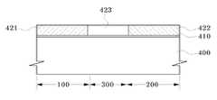
다음에 도 5를 참조하면, 주입된 p형 불순물이온 및 n형 불순물이온의 활성화를 위한 어닐링을 수행한다. 이 어닐링에 의해 제1 영역(100) 및 제2 영역(200)에는 각각 p형으로 도핑된 제1 게이트도전막(421) 및 n형으로 도핑된 제2 게이트도전막(422)이 형성된다. 어닐링에 의해 불순물이온이 활성화되는 과정에서, 제1 영역(100)과 제2 영역(200) 사이의 제3 영역(300)에는 확산 차단막(423)이 존재하므로, 제1 영역(100) 내의 p형 불순물이온과 제2 영역(200) 내의 n형 불순물이온의 상호 확산은 발생되지 않는다.Next, referring to FIG. 5, annealing is performed to activate the implanted p-type impurity ions and n-type impurity ions. By the annealing, the first gate
지금까지 설명한 바와 같이, 본 발명에 따른 반도체소자의 듀얼게이트 형성방법에 따르면, 불순물이온의 활성화를 위한 어닐링 이전에 p형 트랜지스터영역과 n형 트랜지스터영역 사이의 경계영역에 확산 차단막을 형성함으로써, 어닐링시 p형 불순물이온과 n형 불순물이온의 상호 확산을 억제할 수 있다는 이점이 제공된다.As described so far, according to the method for forming a dual gate of a semiconductor device according to the present invention, by annealing by forming a diffusion blocking film in the boundary region between the p-type transistor region and the n-type transistor region before annealing for activation of impurity ions The advantage of suppressing interdiffusion of p-type impurity ions and n-type impurity ions is provided.
이상 본 발명을 바람직한 실시예를 들어 상세하게 설명하였으나, 본 발명은 상기 실시예에 한정되지 않으며, 본 발명의 기술적 사상 내에서 당 분야에서 통상의 지식을 가진 자에 의하여 여러 가지 변형이 가능함은 당연하다.Although the present invention has been described in detail with reference to preferred embodiments, the present invention is not limited to the above embodiments, and various modifications may be made by those skilled in the art within the technical spirit of the present invention. Do.
Claims (10)
Translated fromKoreanPriority Applications (1)
| Application Number | Priority Date | Filing Date | Title |
|---|---|---|---|
| KR1020060059915AKR100732774B1 (en) | 2006-06-29 | 2006-06-29 | Dual gate formation method of semiconductor device |
Applications Claiming Priority (1)
| Application Number | Priority Date | Filing Date | Title |
|---|---|---|---|
| KR1020060059915AKR100732774B1 (en) | 2006-06-29 | 2006-06-29 | Dual gate formation method of semiconductor device |
Publications (1)
| Publication Number | Publication Date |
|---|---|
| KR100732774B1true KR100732774B1 (en) | 2007-06-27 |
Family
ID=38373548
Family Applications (1)
| Application Number | Title | Priority Date | Filing Date |
|---|---|---|---|
| KR1020060059915AExpired - Fee RelatedKR100732774B1 (en) | 2006-06-29 | 2006-06-29 | Dual gate formation method of semiconductor device |
Country Status (1)
| Country | Link |
|---|---|
| KR (1) | KR100732774B1 (en) |
Cited By (1)
| Publication number | Priority date | Publication date | Assignee | Title |
|---|---|---|---|---|
| KR101517384B1 (en) | 2007-10-15 | 2015-05-06 | 삼성전자 주식회사 | Semiconductor gate structure fabrication method |
Citations (1)
| Publication number | Priority date | Publication date | Assignee | Title |
|---|---|---|---|---|
| KR20010065915A (en)* | 1999-12-30 | 2001-07-11 | 박종섭 | A method for forming dual-implanted polysilicon gate of semiconductor device |
- 2006
- 2006-06-29KRKR1020060059915Apatent/KR100732774B1/ennot_activeExpired - Fee Related
Patent Citations (1)
| Publication number | Priority date | Publication date | Assignee | Title |
|---|---|---|---|---|
| KR20010065915A (en)* | 1999-12-30 | 2001-07-11 | 박종섭 | A method for forming dual-implanted polysilicon gate of semiconductor device |
Cited By (1)
| Publication number | Priority date | Publication date | Assignee | Title |
|---|---|---|---|---|
| KR101517384B1 (en) | 2007-10-15 | 2015-05-06 | 삼성전자 주식회사 | Semiconductor gate structure fabrication method |
Similar Documents
| Publication | Publication Date | Title |
|---|---|---|
| KR100391959B1 (en) | Semiconductor apparatus and method of manufacture | |
| KR100324931B1 (en) | Method of Fabricating a Twin Well CMOS Device | |
| KR20060013110A (en) | Manufacturing method of semiconductor device | |
| KR100732774B1 (en) | Dual gate formation method of semiconductor device | |
| KR20010016838A (en) | Method of forming impurity doped region of MOS transistor | |
| KR100508867B1 (en) | Method for fabricating the p-channel MOS transistor and CMOS transistor | |
| KR20030063095A (en) | Semiconductor devices and their fabrication methods | |
| US20080286920A1 (en) | Method for manufacturing semiconductor device | |
| US20050054182A1 (en) | Method for suppressing boron penetration by implantation in P+ MOSFETS | |
| KR100668748B1 (en) | Method of manufacturing semiconductor device using gate-through ion implantation | |
| KR100685879B1 (en) | Semiconductor device and manufacturing method | |
| KR100521439B1 (en) | Method for fabricating the p-channel MOS transistor | |
| US7186631B2 (en) | Method for manufacturing a semiconductor device | |
| KR100632043B1 (en) | Manufacturing method of MOS transistor of semiconductor device | |
| KR20010065915A (en) | A method for forming dual-implanted polysilicon gate of semiconductor device | |
| KR19990085480A (en) | Manufacturing Method of Double Voltage Morse Transistors | |
| KR100271801B1 (en) | Manufacturing Method of Semiconductor Device | |
| KR100529656B1 (en) | Method for fabricating the MOS transistor | |
| KR20010045183A (en) | Method for manufacturing dual gate electrodes of CMOS device | |
| KR100448591B1 (en) | Method of manufacturing a transistor in a semiconductor | |
| KR20010065907A (en) | A method for forming dual-implanted polysilicon gate of semiconductor device | |
| CN100428443C (en) | Method for reducing wafer charge damage | |
| KR100546939B1 (en) | Method for manufacturing high voltage transistor of flash memory device | |
| KR100636912B1 (en) | Dual gate formation method of semiconductor device | |
| KR100745930B1 (en) | Manufacturing Method of Semiconductor Device |
Legal Events
| Date | Code | Title | Description |
|---|---|---|---|
| A201 | Request for examination | ||
| PA0109 | Patent application | St.27 status event code:A-0-1-A10-A12-nap-PA0109 | |
| PA0201 | Request for examination | St.27 status event code:A-1-2-D10-D11-exm-PA0201 | |
| E701 | Decision to grant or registration of patent right | ||
| PE0701 | Decision of registration | St.27 status event code:A-1-2-D10-D22-exm-PE0701 | |
| GRNT | Written decision to grant | ||
| PR0701 | Registration of establishment | St.27 status event code:A-2-4-F10-F11-exm-PR0701 | |
| PR1002 | Payment of registration fee | St.27 status event code:A-2-2-U10-U11-oth-PR1002 Fee payment year number:1 | |
| PG1601 | Publication of registration | St.27 status event code:A-4-4-Q10-Q13-nap-PG1601 | |
| PR1001 | Payment of annual fee | St.27 status event code:A-4-4-U10-U11-oth-PR1001 Fee payment year number:4 | |
| FPAY | Annual fee payment | Payment date:20110526 Year of fee payment:5 | |
| PR1001 | Payment of annual fee | St.27 status event code:A-4-4-U10-U11-oth-PR1001 Fee payment year number:5 | |
| PN2301 | Change of applicant | St.27 status event code:A-5-5-R10-R13-asn-PN2301 St.27 status event code:A-5-5-R10-R11-asn-PN2301 | |
| LAPS | Lapse due to unpaid annual fee | ||
| PC1903 | Unpaid annual fee | St.27 status event code:A-4-4-U10-U13-oth-PC1903 Not in force date:20120621 Payment event data comment text:Termination Category : DEFAULT_OF_REGISTRATION_FEE | |
| PN2301 | Change of applicant | St.27 status event code:A-5-5-R10-R13-asn-PN2301 St.27 status event code:A-5-5-R10-R11-asn-PN2301 | |
| PC1903 | Unpaid annual fee | St.27 status event code:N-4-6-H10-H13-oth-PC1903 Ip right cessation event data comment text:Termination Category : DEFAULT_OF_REGISTRATION_FEE Not in force date:20120621 | |
| PN2301 | Change of applicant | St.27 status event code:A-5-5-R10-R13-asn-PN2301 St.27 status event code:A-5-5-R10-R11-asn-PN2301 | |
| P22-X000 | Classification modified | St.27 status event code:A-4-4-P10-P22-nap-X000 | |
| P22-X000 | Classification modified | St.27 status event code:A-4-4-P10-P22-nap-X000 |