KR100729358B1 - Flash memory device with multi-buffer program scheme - Google Patents
Flash memory device with multi-buffer program schemeDownload PDFInfo
- Publication number
- KR100729358B1 KR100729358B1KR1020050079453AKR20050079453AKR100729358B1KR 100729358 B1KR100729358 B1KR 100729358B1KR 1020050079453 AKR1020050079453 AKR 1020050079453AKR 20050079453 AKR20050079453 AKR 20050079453AKR 100729358 B1KR100729358 B1KR 100729358B1
- Authority
- KR
- South Korea
- Prior art keywords
- buffer
- data
- address
- program
- input
- Prior art date
- Legal status (The legal status is an assumption and is not a legal conclusion. Google has not performed a legal analysis and makes no representation as to the accuracy of the status listed.)
- Expired - Fee Related
Links
Images


Classifications
- G—PHYSICS
- G11—INFORMATION STORAGE
- G11C—STATIC STORES
- G11C16/00—Erasable programmable read-only memories
- G11C16/02—Erasable programmable read-only memories electrically programmable
- G11C16/06—Auxiliary circuits, e.g. for writing into memory
- G11C16/10—Programming or data input circuits
- G—PHYSICS
- G11—INFORMATION STORAGE
- G11C—STATIC STORES
- G11C16/00—Erasable programmable read-only memories
- G11C16/02—Erasable programmable read-only memories electrically programmable
- G11C16/06—Auxiliary circuits, e.g. for writing into memory
- G—PHYSICS
- G11—INFORMATION STORAGE
- G11C—STATIC STORES
- G11C2216/00—Indexing scheme relating to G11C16/00 and subgroups, for features not directly covered by these groups
- G11C2216/12—Reading and writing aspects of erasable programmable read-only memories
- G11C2216/14—Circuits or methods to write a page or sector of information simultaneously into a nonvolatile memory, typically a complete row or word line in flash memory
- G—PHYSICS
- G11—INFORMATION STORAGE
- G11C—STATIC STORES
- G11C2216/00—Indexing scheme relating to G11C16/00 and subgroups, for features not directly covered by these groups
- G11C2216/12—Reading and writing aspects of erasable programmable read-only memories
- G11C2216/22—Nonvolatile memory in which reading can be carried out from one memory bank or array whilst a word or sector in another bank or array is being erased or programmed simultaneously
Landscapes
- Read Only Memory (AREA)
Abstract
Translated fromKorean
Description
Translated fromKorean도 1은 일반적인 멀티 버퍼 프로그램 동작을 설명하는 타이밍도;1 is a timing diagram illustrating a general multi buffer program operation;
도 2는 본 발명의 제 1 실시예에 따른 플래시 메모리 장치를 보여주는 블록도;2 is a block diagram showing a flash memory device according to a first embodiment of the present invention;
도 3a는 본 발명의 제 1 실시예에 따른 플래시 메모리 장치의 어드레스 입력회로의 일 실시예를 보여주는 블록도;3A is a block diagram showing an embodiment of an address input circuit of a flash memory device according to a first embodiment of the present invention;
도 3b는 본 발명의 제 1 실시예에 따른 플래시 메모리 장치의 어드레스 입력회로의 다른 실시예를 보여주는 블록도;3B is a block diagram showing another embodiment of the address input circuit of the flash memory device according to the first embodiment of the present invention;
도 4는 본 발명의 제 2 실시예에 따른 플래시 메모리 장치를 보여주는 블록도;4 is a block diagram showing a flash memory device according to a second embodiment of the present invention;
도 5a는 본 발명의 제 2 실시예에 따른 플래시 메모리 장치의 어드레스 입력회로의 일 실시예를 보여주는 블록도;5A is a block diagram showing an embodiment of an address input circuit of a flash memory device according to a second embodiment of the present invention;
도 5b는 본 발명의 제 2 실시예에 따른 플래시 메모리 장치의 어드레스 입력회로의 다른 실시예를 보여주는 블록도;Fig. 5B is a block diagram showing another embodiment of the address input circuit of the flash memory device according to the second embodiment of the present invention;
도 6은 본 발명에 따른 플래시 메모리 장치의 멀티 버퍼 로드 동작을 설명하는 타이밍도이다.6 is a timing diagram illustrating a multi-buffer load operation of a flash memory device according to the present invention.
*도면의 주요부분에 대한 부호의 설명** Explanation of symbols for main parts of drawings *
10 : 어드레스 입력 회로11 : 초기 어드레스 래치10: address input circuit 11: initial address latch
12 : 입력 어드레스 래치13 : 비교기12: input address latch 13: comparator
14 : 카운터15 : 지연회로14
16 : 래치20 : 멀티 버퍼16: latch 20: multi-buffer
30 : 제어 로직40 : 출력 버퍼 제어 회로30: control logic 40: output buffer control circuit
50 : 셀 어레이60 : 기입 회로50
70 : 리드 회로80 : 리드 데이터 버퍼70: read circuit 80: read data buffer
90 : 출력 버퍼100 : 상태 데이터 버퍼90: output buffer 100: status data buffer
본 발명은 반도체 메모리 장치에 관한 것으로, 더욱 상세하게는 멀티 버퍼 프로그램 스킴을 갖는 플래시 메모리 장치에 관한 것이다.The present invention relates to a semiconductor memory device, and more particularly to a flash memory device having a multi-buffer program scheme.
일반적으로 플래시 메모리 장치(flash memory device)는 전기적으로 프로그램 및 소거 동작이 가능한 불휘발성 반도체 메모리 장치로, 모바일 기기의 대용량 저장장치나 코드 메모리(Coded Memory) 등의 적용에서도 많은 호응을 얻고 있다. 플래시 메모리 장치는 낸드형(NAND type)과 노어형(NOR type) 플래시 메모리 장치로 분류될 수 있다. 노어형 플래시 메모리 장치의 셀 어레이는 하나의 비트 라인에 복수 개의 메모리 셀들이 병렬로 배열되는 구조를 갖는다. 반면에 낸드형 플래시 메모리 장치의 셀 어레이는 하나의 비트 라인에 복수 개의 메모리 셀들이 직렬로 배열되는 구조를 갖는다. 낸드형 플래시 메모리와 비교할 때, 노어형 플래시 메모리 장치는 프로그램 및 읽기 동작에 있어서 월등하게 빠른 속도 특성을 가지고 있다. 노어형 플래시 메모리 장치는 프로그램 속도를 더욱 향상시키기 위해서 멀티 버퍼 프로그램 방식을 지원한다. 특히 멀티 버퍼 프로그램 방식에 따르면, 대용량의 프로그램 데이터가 멀티 버퍼에 먼저 로드되고, 멀티 버퍼에 로드된 대용량 데이터가 그 다음에 셀 어레이에 프로그램된다.In general, a flash memory device is a nonvolatile semiconductor memory device that can be electrically programmed and erased, and has been widely used in applications such as mass storage devices and coded memories of mobile devices. Flash memory devices may be classified into NAND type and NOR type flash memory devices. A cell array of a NOR flash memory device has a structure in which a plurality of memory cells are arranged in parallel on one bit line. In contrast, a cell array of a NAND flash memory device has a structure in which a plurality of memory cells are arranged in one bit line in series. Compared to NAND flash memory, NOR flash memory devices have a superior speed characteristic for program and read operations. NOR flash memory devices support multi-buffer programming to further improve program speed. In particular, according to the multi-buffer program method, a large amount of program data is loaded into a multi-buffer first, and a large amount of data loaded into the multi-buffer is then programmed into a cell array.
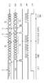
도 1은 일반적인 플래시 메모리 장치의 멀티 버퍼 프로그램 방식을 설명하기 위한 타이밍도이다. 도 1을 참조하면, 노어형 플래시 메모리 장치의 멀티 버퍼 프로그램 방식은 칩 인에이블 신호(nCE)가 로우 레벨로 활성화되고 쓰기 인에이블 신호(nWE)가 토글(Toggle)됨에 따라 프로그램 시작 명령어(CMD1)가 플래시 메모리 장치에 입력된다. 일반적으로 프로그램 시작 명령어(CMD1)는 쓰기 인에이블 신호(nWE)의 천이에 동기되어 어드레스(A0~A1)와 데이터(DO~D1)를 통해서 입력된다. 이후 프로그램 어드레스(PA)와 프로그램 데이터(PD)가 쓰기 인에이블 신호(nWE)의 천이에 동기되어 입력된다. 셀 어레이에 프로그램될 데이터는 멀티 버퍼의 용량만큼 입력된다. 예를 들면, 만일 멀티 버퍼가 128W(W:워드 단위를 나타냄)의 크기를 갖고, 입출력 비트 구조가 x16이라면, 멀티 버퍼로 128W의 프로그램 데이터를 로드하기 위해서는 쓰기 인에이블 신호(nWE)가 128번 토글되어야 한다. 도 1에 도시된 바와 같이 빗금 친 프로그램 어드레스(PA)와 프로그램 데이터(PD)가 쓰기 인에이블 신호(nWE)의 128번 토글에 의해 멀티 버퍼로 로드될 것이다.1 is a timing diagram illustrating a multi-buffer program method of a general flash memory device. Referring to FIG. 1, in the multi-buffer program method of a NOR flash memory device, a program start command CMD1 is generated as the chip enable signal nCE is activated at a low level and the write enable signal nWE is toggled. Is input to the flash memory device. In general, the program start command CMD1 is input through the addresses A0 to A1 and the data DO to D1 in synchronization with the transition of the write enable signal nWE. Thereafter, the program address PA and the program data PD are input in synchronization with the transition of the write enable signal nWE. Data to be programmed into the cell array is input by the capacity of the multi-buffer. For example, if the multi-buffer has a size of 128W (W: word unit) and the input / output bit structure is x16, the write enable signal nWE is 128 to load 128W of program data into the multi-buffer. Should be toggled As shown in FIG. 1, the hatched program address PA and the program data PD may be loaded into the multi-buffer by the toggle 128 of the write enable signal nWE.
종래의 멀티 버퍼 프로그램 방식에 따르면, 도 1에 도시된 바와 같이, 멀티버퍼로 프로그램 데이터가 로드되는 구간(tL) 동안 셀 어레이에 저장된 데이터가 외부로 출력될 수 있다. 이는 쓰기 인에이블 신호(nWE)의 토글이 중지된 상태에서 출력 인에이블 신호(nOE)를 로우로 천이함으로 가능하다. 출력 인에이블 신호(nOE)의 천이에 동기되어 입력된 어드레스(RA1)에 따라 셀 어레이로부터 독출된 데이터(RD1)가 외부로 출력된다. 마찬가지로, 쓰기 인에이블 신호(nWE)의 토글이 중지된 상태에서 출력 인에이블 신호(nOE)가 로우로 천이할 때 입력된 어드레스(RA2)에 따라 셀 어레이로부터 독출된 데이터(RD2)가 외부로 출력된다.According to the conventional multi-buffer program method, as illustrated in FIG. 1, data stored in a cell array may be output to the outside during a period tL in which program data is loaded into the multi-buffer. This is possible by shifting the output enable signal nOE low while the toggle of the write enable signal nWE is stopped. The data RD1 read from the cell array is output to the outside according to the address RA1 input in synchronization with the transition of the output enable signal nOE. Similarly, when the output enable signal nOE transitions low while the toggle of the write enable signal nWE is stopped, the data RD2 read from the cell array is output to the outside according to the input address RA2. do.
어드레스 (RA1, RA2)가 현재 멀티 버퍼에 로드된 데이터의 프로그램될 셀 어레이를 가리키는 어드레스인 경우, 프로그램 데이터의 로드 구간(tL) 동안 출력되는 데이터(RD1, RD2)(도면에 ①, ②로 표시됨)는 프로그램을 위해 이미 소거된 셀들의 데이터이다. 만일 프로그램 대상이 아닌 다른 뱅크 어드레스나 블록 어드레스를 입력하게 되면 그에 해당하는 저장된 데이터가 출력될 것이다.When the addresses RA1 and RA2 are addresses indicating the cell array to be programmed of the data currently loaded into the multi-buffer, the data RD1 and RD2 outputted during the load period tL of the program data are indicated by ① and ② in the drawing. Is the data of cells already erased for the program. If you enter a bank address or block address other than the program target, the corresponding stored data will be output.
일단 프로그램 데이터가 모두 멀티 버퍼에 로드되면, 프로그램 확정 명령(Program confirm command : CMD2)이 쓰기 인에이블 신호(nWE)의 천이에 동기되어 입력된다. 이후, 도 1에 도시된 바와 같이, 출력 인에이블 신호(nOE)의 천이에 동기되어 어드레스(RA3)가 입력되면, 플래시 메모리 장치는 프로그램 비지 상태를 나타내는 상태 데이터(SD)(도면에 ③로 표기됨)가 출력된다. 앞서 설명된 바와 같이 종래 기술에 따른 멀티 버퍼 프로그램 방식에 따르면, 프로그램 데이터가 로드되는 동안 셀 어레이에 저장된 데이터를 출력하는 것이 가능하다.Once all of the program data is loaded into the multi-buffer, a program confirm command (CMD2) is input in synchronization with the transition of the write enable signal nWE. Subsequently, as shown in FIG. 1, when the address RA3 is input in synchronization with the transition of the output enable signal nOE, the flash memory device denotes state data SD (3 in the drawing) indicating a program busy state. Is displayed. As described above, according to the conventional multi-buffer program method, it is possible to output data stored in the cell array while program data is loaded.
따라서, 본 발명은 프로그램 데이터의 로드 구간 동안 셀 데이터 이외의 플래시 메모리 장치의 내부 상태 정보를 외부로 출력할 수 있는 기술을 제공하는 데 있다.Accordingly, an aspect of the present invention is to provide a technique for outputting internal state information of a flash memory device other than cell data to an external device during a load period of program data.
본 발명의 목적은 프로그램 데이터의 로드 구간 동안 내부 상태 정보 및 셀 데이터 정보를 출력하는 플래시 메모리 장치 및 그 방법을 제공하는 데 있다.An object of the present invention is to provide a flash memory device and a method for outputting internal state information and cell data information during a load period of program data.
본 발명의 목적은 프로그램 데이터의 로드 구간 동안 멀티 버퍼의 로드 상태 정보를 출력하는 플래시 메모리 장치 및 그 방법을 제공하는 데 있다.An object of the present invention is to provide a flash memory device and a method for outputting load state information of a multi-buffer during a load period of program data.
상술한 제반 목적을 달성하기 위한 일 실시예에 따른 본 발명의 메모리 장치는 프로그램될 복수의 데이터가 로드되는 제 1 버퍼; 상기 제 1 버퍼의 로드 상태 정보를 실시간으로 저장하는 제 2 버퍼; 상기 제 1 버퍼로의 데이터 로드 중에 제어신호에 응답하여 상기 로드 상태 정보가 출력되도록 상기 제 2 버퍼의 출력을 활성화하는 버퍼 제어회로를 포함한다.In accordance with an aspect of the present invention, there is provided a memory device including a first buffer into which a plurality of data to be programmed is loaded; A second buffer configured to store load state information of the first buffer in real time; And a buffer control circuit for activating the output of the second buffer such that the load state information is output in response to a control signal during data loading into the first buffer.
바람직한 실시예에 있어서, 상기 제 1 버퍼는 상기 복수의 데이터 이외에 상기 복수의 데이터와 대응하는 어드레스를 입력받는다.In a preferred embodiment, the first buffer receives an address corresponding to the plurality of data in addition to the plurality of data.
바람직한 실시예에 있어서, 상기 로드 상태 정보는 상기 제 1 버퍼에 로드되는 데이터와 데이터의 카운터 값, 프로그램 시작 명령의 유무, 로드의 종료 여부를 포함하는 정보이다.In a preferred embodiment, the load state information is information including data loaded into the first buffer and a counter value of data, whether a program start command exists, and whether or not the load is finished.
바람직한 실시예에 있어서, 상기 메모리 장치는 노어 플래시 메모리인 것을 특징으로 한다.In a preferred embodiment, the memory device is a NOR flash memory.
상술한 제반 목적을 달성하기 위한 본 발명의 다른 특징에 따르면, 프로그램될 복수의 데이터가 로드되는 제 1 버퍼; 상기 복수의 데이터와 대응하는 외부 어드레스를 상기 제 1 버퍼의 어드레스로 공급하는 어드레스 입력 회로; 상기 제 1 버퍼의 로드 상태 정보를 저장하는 제 2 버퍼; 프로그램 시작 명령에 응답하여 상기 제 1 버퍼로 상기 복수의 데이터를 로드하고, 상기 제 1 버퍼로의 데이터 로드 중에 외부 제어신호와 상기 외부 어드레스에 응답하여 상기 로드 상태 정보를 출력하도록 상기 제 2 버퍼의 출력을 활성화하는 제어회로를 포함한다.According to another aspect of the present invention for achieving the above object, a first buffer is loaded with a plurality of data to be programmed; An address input circuit for supplying an external address corresponding to the plurality of data to an address of the first buffer; A second buffer for storing load state information of the first buffer; Load the plurality of data into the first buffer in response to a program start command, and output the load state information in response to an external control signal and the external address during data loading into the first buffer; And a control circuit that activates the output.
바람직한 실시예에 있어서, 상기 복수의 데이터는 데이터의 입출력 단위의 복수 배 크기이다.In a preferred embodiment, the plurality of data is a plurality of times the input and output unit of the data.
바람직한 실시예에 있어서, 상기 어드레스 입력 회로는 입력되는 상기 외부 어드레스로부터 상기 제 1 버퍼의 어드레스를 생성하는 어드레스 생성기와; 실시간 입력되는 상기 외부 어드레스와 최초로 입력된 외부 어드레스를 비교하여 비교 신호로 출력하는 비교기를 포함한다.In an exemplary embodiment, the address input circuit includes an address generator for generating an address of the first buffer from the external address to be input; And a comparator for comparing the external address input in real time with the external address input first and outputting the comparison signal.
바람직한 실시예에 있어서, 상기 어드레스 입력 회로는 상기 제 1 버퍼로 로드되는 데이터의 수를 카운트하는 카운터를 더 포함한다.In a preferred embodiment, the address input circuit further comprises a counter for counting the number of data loaded into the first buffer.
바람직한 실시예에 있어서, 상기 비교기는 입력되는 상기 외부 어드레스를 래치하는 제 1 래치와; 입력되는 상기 외부 어드레스 중 최초 어드레스를 래치하는 제 2 래치와; 상기 제 1 래치와 상기 제 2 래치에 래치된 어드레스를 비교하여 비교 신호로 출력하는 비교 회로를 포함한다.In a preferred embodiment, the comparator comprises: a first latch for latching the external address input; A second latch for latching an initial address of the external addresses to be input; And a comparison circuit that compares the address latched in the first latch and the second latch and outputs a comparison signal.
바람직한 실시예에 있어서, 상기 비교기는 입력되는 상기 외부 어드레스를 래치하는 제 1 래치와; 상기 외부 어드레스가 한 클록 지연된 어드레스를 래치하는 제 2 래치와; 상기 제 1 래치와 상기 제 2 래치에 래치된 어드레스를 비교하여 비교 신호로 출력하는 비교 회로를 포함한다.In a preferred embodiment, the comparator comprises: a first latch for latching the external address input; A second latch for latching an address of which the external address is delayed by one clock; And a comparison circuit that compares the address latched in the first latch and the second latch and outputs a comparison signal.
바람직한 실시예에 있어서, 상기 비교 회로는 비교되는 두 어드레스가 동일한 버퍼링 단위 어드레스인지 혹은 버퍼링 중인 어드레스와 관계없는 어드레스인지를 검출한다.In a preferred embodiment, the comparison circuit detects whether two addresses being compared are the same buffering unit address or an address independent of the address being buffered.
바람직한 실시예에 있어서, 상기 상태 정보는 상기 어드레스 카운터로부터 출력되는 카운트 값과 상기 프로그램 시작 명령의 입력 여부와 버퍼 로드가 종료되고 셀 어레이로의 프로그램 중임을 나타내는 프로그램 비지 신호를 포함한다.In a preferred embodiment, the state information includes a count value output from the address counter, a program busy signal indicating whether the program start command is input, and a buffer load is finished and programming to the cell array.
바람직한 실시예에 있어서, 상기 상태 정보는 상기 제 1 버퍼에 로드된 복수의 데이터 중 상기 외부 어드레스에 대응하는 데이터와, 상기 프로그램 시작 명령의 입력 여부와, 버퍼 로드가 종료되고 셀 어레이로의 프로그램 중임을 나타내는 프로그램 비지 신호를 포함한다.In a preferred embodiment, the state information includes data corresponding to the external address among a plurality of data loaded in the first buffer, whether or not the program start command is input, buffer loading is completed, and programming into the cell array. It includes a program busy signal indicating.
바람직한 실시예에 있어서, 상기 메모리 장치는 노어 플래시 메모리이다.In a preferred embodiment, the memory device is a NOR flash memory.
바람직한 실시예에 있어서, 상기 외부 제어신호는 쓰기 인에이블 신호(nWE)와 출력 인에이블 신호(nOE)를 포함한다.In an exemplary embodiment, the external control signal includes a write enable signal nWE and an output enable signal nOE.
바람직한 실시예에 있어서, 상기 상태 정보를 출력하기 위해서는 쓰기 인에이블 신호(nWE)를 하이로 유지하고, 출력 인에이블 신호(nOE)를 로우로 천이하는 것을 특징으로 한다.In an exemplary embodiment, the write enable signal nWE is kept high and the output enable signal nOE is transitioned low to output the state information.
바람직한 실시예에 있어서, 상기 메모리 장치는 입력되는 외부 어드레스가 상기 제 1 버퍼에 로드된 데이터들과 대응하는 어드레스이면 상기 로드 상태 정보를, 그렇지 않은 경우에는 상기 외부 어드레스에 대응하는 셀 어레이의 데이터가 출력된다.In example embodiments, the memory device may read the load state information if the external address input corresponds to data loaded in the first buffer, and if not, the data of the cell array corresponding to the external address. Is output.
상술한 제반 목적을 달성하기 위한 본 발명의 또 다른 특징에 따른 메모리 장치는, 버퍼 어드레스에 응답하여 일련의 프로그램 데이터들을 입력받는 멀티 버퍼와; 외부 어드레스의 입력에 응답하여 상기 버퍼 어드레스로 공급하며, 현재 입력되는 외부 어드레스가 기준 어드레스와 일치하는지의 여부를 나타내는 비교 신호를 발생하는 어드레스 입력회로와; 상기 멀티 버퍼에 로드되는 데이터를 포함하는 로드 상태 정보를 저장하는 상태 데이터 버퍼와; 상기 로드 상태 정보가 외부로 출력되도록 상기 비교 신호에 응답하여 출력 버퍼를 제어하는 버퍼 제어 회로를 포함한다.According to still another aspect of the present invention, there is provided a memory device including: a multi buffer configured to receive a series of program data in response to a buffer address; An address input circuit for supplying to the buffer address in response to an input of an external address, and generating a comparison signal indicating whether or not the currently input external address matches the reference address; A state data buffer for storing load state information including data loaded into the multi-buffer; And a buffer control circuit for controlling an output buffer in response to the comparison signal so that the load state information is output to the outside.
바람직한 실시예에 있어서, 상기 기준 어드레스는 상기 멀티 버퍼에 최초로 로드되는 데이터의 외부 어드레스이다.In a preferred embodiment, the reference address is an external address of data initially loaded into the multi-buffer.
바람직한 실시예에 있어서, 상기 기준 어드레스는 상기 현재 입력되는 외부 어드레스의 바로 이전에 입력된 외부 어드레스이다.In a preferred embodiment, the reference address is an external address input immediately before the currently input external address.
바람직한 실시예에 있어서, 상기 로드 상태 정보는 상기 멀티 버퍼에 로드 완료된 상기 일련의 프로그램 데이터가 셀 어레이로의 프로그램이 수행되는지의 여부를 나타내는 프로그램 비지(Program Busy) 상태 데이터를 포함한다.In a preferred embodiment, the load state information includes program busy state data indicating whether the series of program data loaded into the multi-buffer program is executed in a cell array.
바람직한 실시예에 있어서, 상기 로드 상태 정보는 상기 멀티 버퍼에 로드되 는 프로그램 데이터의 카운트 수를 포함한다.In a preferred embodiment, the load state information includes a count number of program data loaded into the multi buffer.
바람직한 실시예에 있어서, 상기 버퍼 제어 회로는 셀 데이터가 외부로 출력되도록 상기 비교 신호에 응답하여 상기 메모리 장치의 독출 회로를 제어한다.In a preferred embodiment, the buffer control circuit controls the read circuit of the memory device in response to the comparison signal so that cell data is output to the outside.
상기 제반 목적을 달성하기 위한 본 발명의 메모리 장치의 프로그램 방법은, 프로그램될 복수의 데이터를 버퍼에 로드하는 메모리 장치에 있어서, 상기 복수의 데이터를 상기 버퍼로 로드하는 중에 데이터 로드를 일시 중지하고, 상기 버퍼에 로드된 데이터와 상기 버퍼에 로드된 데이터의 카운트 수를 포함하는 로드 상태정보를 출력 받는 것을 특징으로 한다.In the memory device of the present invention to achieve the above object, a memory device for loading a plurality of data to be programmed into a buffer, the data load is suspended while loading the plurality of data into the buffer, And load status information including the data loaded in the buffer and the count number of the data loaded in the buffer.
바람직한 실시예에 있어서, 상기 로드 상태 정보는 입력된 명령어에 대한 정보도 포함한다.In a preferred embodiment, the load state information also includes information on the input command.
상술한 제반 목적을 달성하기 위한 본 발명의 또 다른 특징에 따르면, 복수의 프로그램 데이터를 멀티 버퍼에 로드하여 셀 어레이로 기입하는 프로그램 방식의 메모리 장치에 있어서, 프로그램 시작 명령을 입력하는 단계와; 상기 프로그램 시작 명령에 응답하여 상기 복수의 프로그램 데이터와 각 데이터에 대응하는 어드레스가 멀티 버퍼로 로드되는 단계와; 로드가 종료되고, 로드된 상기 복수의 프로그램 데이터를 상기 셀 어레이에 기입되도록 프로그램 확정(Program Confirm) 명령을 입력하는 단계와; 로드된 상기 복수의 데이터가 셀 어레이로 프로그램되는 단계를 포함하되, 상기 프로그램 시작 명령이 입력된 이후부터의 상기 멀티 버퍼의 로드 상태 정보를 외부 제어신호와 어드레스를 통해 확인할 수 있다.According to still another aspect of the present invention for achieving the above object, a program type memory device for loading a plurality of program data in a multi-buffer to write to a cell array, comprising: inputting a program start command; Loading the plurality of program data and an address corresponding to each data into a multi-buffer in response to the program start command; Terminating a load and inputting a program confirm command to write the plurality of loaded program data into the cell array; And loading the plurality of loaded data into a cell array, wherein load state information of the multi-buffer since the program start command is input can be confirmed through an external control signal and an address.
바람직한 실시예에 있어서, 상기 로드 상태 정보는 상기 복수의 프로그램 데 이터 중 상기 멀티 버퍼에 로드된 데이터의 카운트 수와 입력된 명령어에 대한 정보를 포함한다.In a preferred embodiment, the load state information includes information about a count number of data loaded in the multi-buffer of the plurality of program data and an input command.
바람직한 실시예에 있어서, 상기 로드 상태 정보는 상기 복수의 프로그램 데이터 중 상기 멀티 버퍼에 로드된 데이터와 입력된 명령어에 대한 정보를 포함한다.In a preferred embodiment, the load state information includes information about the data loaded in the multi-buffer and the input command of the plurality of program data.
바람직한 실시예에 있어서, 상기 프로그램 방법은 상기 어드레스가 상기 멀티 버퍼에 로드된 데이터들과 대응하는 어드레스이면 상기 로드 상태 정보를, 그렇지 않은 경우에는 상기 어드레스에 대응하는 셀 어레이의 데이터가 출력된다.In a preferred embodiment, the program method outputs the load state information if the address corresponds to data loaded in the multi-buffer; otherwise, data of a cell array corresponding to the address is output.
바람직한 실시예에 있어서, 상기 로드 상태 정보는 프로그램 확정(Program Confirm)명령의 입력 이후에는 프로그램 비지(Program Busy)임을 나타내는 정보이다.In a preferred embodiment, the load state information is information indicating that the program is busy after input of a program confirm command.
바람직한 실시예에 있어서, 상기 메모리 장치는 노어 플래시 메모리이다.In a preferred embodiment, the memory device is a NOR flash memory.
바람직한 실시예에 있어서, 상기 외부 제어 신호는 쓰기 인에이블 신호(nWE)와 출력 인에이블 신호(nOE)를 포함하며, 상기 로드 상태 정보를 확인하기 위해서는 쓰기 인에이블 신호(nWE)를 하이, 출력 인에이블 신호(nOE)를 로우로 토글하는 것을 특징으로 한다.In an exemplary embodiment, the external control signal includes a write enable signal nWE and an output enable signal nOE, and the write enable signal nWE is set high and output to verify the load state information. Toggle the enable signal nOE low.
이상의 구성과 방법을 포함하는 본 발명은 프로그램될 데이터의 버퍼로의 로드중에 어드레스와 제어신호의 조작을 통해서 현재 로드되는 상태정보를 외부에서 확인할 수 있는 장치와 방법을 제공한다.The present invention including the above configuration and method provides an apparatus and method for externally checking the state information currently loaded through manipulation of an address and a control signal during loading of a data to be programmed into a buffer.
이하, 본 발명이 속하는 기술분야에서 통상의 지식을 가진 자가 본 발명의 기술적 사상을 용이하게 실시할 수 있을 정도로 상세히 설명하기 위하여, 본 발명의 가장 바람직한 실시예를 첨부된 도면을 참조하여 설명하기로 한다.DETAILED DESCRIPTION Hereinafter, exemplary embodiments of the present invention will be described with reference to the accompanying drawings so that those skilled in the art may easily implement the technical idea of the present invention. do.
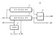
도 2는 본 발명의 제 1 실시예에 따른 메모리 장치를 보여주는 블록도이다.2 is a block diagram illustrating a memory device according to a first embodiment of the present invention.
도 2를 참조하면, 어드레스 입력회로(10)는 외부에서 입력되는 어드레스(ADD)를 셀 어레이(50)와 멀티 버퍼(20)로 데이터를 로드하기 위한 버퍼 어드레스(B_ADD)로 공급한다. 멀티 버퍼(20)로 공급되는 버퍼 어드레스(B_ADD)는 외부로부터 입력되는 어드레스(ADD)로부터 멀티 버퍼(20)의 어드레스에 해당하는 하위 어드레스 비트에 해당하는 값만을 취할 수 있다. 또한, 어드레스 입력회로(10)는 현재 입력된 어드레스와 바로 이전에 입력된 어드레스 혹은 프로그램 시작 명령어(CMD1)의 입력 이후 최초 어드레스를 비교하여 어드레스 비교신호(A_COMP)를 생성한다. 어드레스 입력회로(10)는 또한 버퍼에 로드된 데이터의 수를 의미하는 버퍼 로드 수(B_L_Count)를 상태 데이터 버퍼(100)로 전송한다. 어드레스 입력회로(10)의 구체적인 동작 및 구성은 후술하게 되는 도 3a 및 도 3b에서 설명하게 될 것이다.Referring to FIG. 2, the
멀티 버퍼(20)는 셀 어레이(50)로 프로그램될 데이터가 일시 저장되는 버퍼 메모리이다. 본 발명에서 개시되는 멀티 버퍼(20)는 단지 하나의 입출력 단위(I/O)의 데이터 용량을 가진 버퍼가 아니라 버퍼링 단위가 입출력 단위(I/O)의 복수 배에 해당되는 데이터 용량을 갖는 복수의 버퍼들을 의미한다. 외부로부터 입력되는 프로그램 데이터(PD)가 로드되는 멀티 버퍼(20)에서의 어드레스는 상술한 어드레스 입력회로(10)에 의해서 공급되는 버퍼 어드레스(B_ADD)이다. 멀티 버퍼(20)에 로드되는 데이터의 용량이 128W(예를 들면 I/O 단위가 1 워드인 경우)라면 128개의 버 퍼 어드레스(B_ADD)가 필요할 것이다. 멀티 버퍼(20)로의 모든 데이터 로드가 완료되면, 로드된 데이터는 셀 어레이에 프로그램되기 위해 후술하게 될 기입 회로(60)로 전송될 것이다.The
제어 로직(30)은 외부 제어신호(nCE, nWE, nOE)와 명령어(CMD)에 반응하여 버퍼 로드 스타트 신호(B_L_Start)와 프로그램 비지 신호(P_Busy)를 출력한다. 제어 로직(30)에서 출력되는 버퍼 로드 스타트 및 프로그램 비지 신호(B_L_Start, P_Busy)는 멀티 버퍼(20)의 상태를 나타낸다. 특히 버퍼 로드 스타트 및 프로그램 비지 신호(B_L_Start, P_Busy)는 멀티 버퍼(20)로의 데이터 로드 상태를 의미하는 신호들이다. 각 제어신호에 대한 제어 로직(30)의 동작이 상술한 동작에 국한되지 않음은 이 분야에서 통상의 지식을 습득한 자에게 잘 알려져 있다.The
출력 버퍼 제어회로(40)는 입력되는 출력 인에이블 신호(nOE), 상태 데이터로서 버퍼 로드 스타트 및 프로그램 비지 신호(B_L_Start P_Busy), 그리고 어드레스 비교신호(A_COMP)를 입력받고, 출력 버퍼 제어신호들(RDO_EN, SDO_EN)을 발생한다. 출력 버퍼 제어회로(40)는 입력 신호들에 응답하여 동작하며, 셀 어레이(50)로부터 독출한 리드 데이터(R_Data)를 출력할 것인지 혹은 상태 데이터(S_Data)를 출력할 것인지를 결정한다. 출력 버퍼 제어신호(RDO_EN)는 셀 어레이(50)로부터 독출된 데이터를 출력하도록 출력 버퍼(90) 및 리드 데이터 버퍼(80)를 활성화하고, 출력 버퍼 제어신호(SDO_EN)는 상태 데이터(S_Data)를 출력하도록 상태 데이터 버퍼(100)와 출력 버퍼(90)를 활성화한다. 아래 표 1은 출력 버퍼 제어회로(40)의 제어동작을 설명하기 위한 진리표이다.The output
표 1에서 'H'는 'HIGH', 'L'은 'LOW', 'X'는 'DON'T CARE'를 의미한다. 그리고 출력 인에이블 신호(nOE)가 'L'이 되는 시점에서는 쓰기 인에이블 신호(nWE)는 'H'가 되는 상호 관계를 고려하여 쓰기 인에이블 신호(nWE)에 대한 논리치는 생략하였다.여기서 'L'은 논리 'LOW'를 'H'는 논리 'HIGH'를 의미한다.In Table 1, 'H' means 'HIGH', 'L' means 'LOW', and 'X' means 'DON'T CARE'. When the output enable signal nOE becomes 'L', the logic value of the write enable signal nWE is omitted in consideration of the mutual relationship in which the write enable signal nWE becomes 'H'. L 'means logic' LOW 'and' H 'means logic' HIGH '.
표 1을 참조하면, 어드레스 비교신호(A_COMP)가 'H'이고 출력 인에이블 신호(nOE)가 토글할 때, 출력 버퍼 제어회로(40)는 상태 데이터가 출력되도록 출력 버퍼(90)와 상태 데이터 버퍼(100)를 활성화한다. 즉, 어드레스 비교신호(A_COMP)가 'H'이고 출력 인에이블 신호(nOE)가 토글할 때, 출력 버퍼 제어회로(40)는 출력 버퍼 제어 신호(SDO_EN)을 하이(H)로 활성화시킨다. 그러나 입력되는 어드레스가 상태 데이터의 출력과 무관한 어드레스라면(예를 들면, 어드레스 비교신호(A_COMP)가 'L'이고 출력 인에이블 신호(nOE)가 토글할 때), 출력 버퍼 제어회로(40)는 리드 데이터가 출력 되도록 상술한 출력 버퍼(90)와 리드 데이터 버퍼(80)를 제어한다. 즉, 어드레스 비교신호(A_COMP)가 'L'이고 출력 인에이블 신호(nOE)가 토글할 때, 출력 버퍼 제어회로(40)는 출력 버퍼 제어 신호(RDO_EN)을 하이로 활성화시킨다. 출력 버퍼 제어회로(40)는 프로그램 비지 신호(P_Busy)가 하이로 활성화될 때 출력 버퍼 제어신호(SDO_EN)를 하이로 활성화시킨다. 이때 상태 데이터 버퍼(100)에 저장된 값(예를 들면, 프로그램 비지 신호(P_Busy)의 상태를 나타내는 데이터)이 출력 버퍼(90)를 통해 외부로 출력된다.Referring to Table 1, when the address comparison signal A_COMP is 'H' and the output enable signal nOE is toggled, the output
셀 어레이(50)는 멀티 버퍼(20)로의 데이터 로드가 완료되면, 로드된 데이터가 프로그램되는 셀들과 어드레스(F_ADD)가 행과 열 어드레스로 각각 디코딩되는 디코더를 포함한다. 어드레스(F_ADD)에 대응하는 셀 어레이(50)의 저장 데이터는 리드 회로(70)에 의해서 감지되고 독출될 것이다.The
기입 회로(60)는 멀티 버퍼(20)에 로드된 데이터를 셀 어레이(50)에 순차적으로 프로그램하는 회로이다. 일반적으로 노어(NOR) 플래시 메모리의 경우, 기입 회로(60)는 멀티 버퍼(20)의 로드 데이터를 입력받아 셀 어레이에 입력된 데이터를 프로그램한다. 기입 회로(60)에 대한 제반 구성과 동작은 이 분야에서 통상의 지식을 습득한 자들에게는 자명하기 때문에 구체적 설명은 생략하기로 한다.The
리드 회로(70)는 출력 인에이블 신호(nOE)의 활성화에 동기 되어 입력된 어드레스(ADD)의 셀 어레이 데이터를 독출하는 회로이다. 일반적으로 리드 회로(70)는 감지증폭기와 버퍼를 포함하며 셀의 문턱전압의 상태를 감지하는 방식으로 셀에 저장된 데이터를 독출한다.The
리드 데이터 버퍼(80)는 상술한 리드 회로(70)로부터 출력되는 독출된 데이터가 저장되는 버퍼회로이다. 리드 데이터 버퍼(80)는 출력 버퍼 제어회로(40)에 의해서 제어된다. 리드 데이터 버퍼(80)는 출력 버퍼 제어회로(40)로부터 출력 버퍼 제어신호(RDO_EN)를 입력받으면, 리드 회로(70)로부터 독출된 데이터를 전달받아 저장한다.The read
상태 데이터 버퍼(100)는 프로그램 데이터(PD)가 멀티 버퍼(20)로 로드와 관련된 정보인 상태 데이터가 실시간으로 저장되는 버퍼이다. 상태 데이터는 프로그램 데이터(PD)가 멀티 버퍼(20)에 로드되도록 프로그램 시작(Program Start)명령이 입력되었는지를 알려주는 버퍼 로드 스타트 신호(B_L_Start)를 포함한다. 또한 상태 데이터는 버퍼(20)로의 모든 데이터 로드가 완료되고 로드된 데이터가 셀 어레이에 프로그램되고 있음을 지시하는 프로그램 비지 신호(P_Busy)를 포함한다. 상태 데이터 버퍼(100)에 저장된 데이터는 출력 버퍼 제어회로(40)의 제어에 따라 출력 버퍼(90)를 통해서 외부로 출력된다. 본 발명에서 개시된 상태 데이터는 멀티 버퍼(20)로의 데이터 로드 상태에 대한 정보에만 한정되지는 않으며, 그 이외의 메모리 장치 내부의 상태 정보를 포함할 수 있다.The
출력 버퍼(90)는 리드 데이터 버퍼(80)와 상태 데이터 버퍼(100)로부터 출력되는 데이터를 상술한 출력 버퍼 제어회로(40)의 제어에 따라 선택적으로 입력받아 출력하는 버퍼이다. 출력 버퍼(90)의 선택적인 입력과 출력은 상술한 출력 버퍼 제어회로(40)의 제어신호(RDO_EN, SDO_EN)에 의거하여 제어된다. 출력 버퍼 제어 신호(RDO_EN)가 활성화되면, 리드 데이터 버퍼(80)는 셀 데이터를 입력받아 저장하고, 리드 데이터 버퍼(80)에 저장된 데이터는 출력 버퍼(90)를 통해 외부로 출력된다. 반면에 출력 버퍼 제어신호(SDO_EN)가 활성화되면, 상태 데이터 버퍼(100)에 실시간으로 래치되는 상태 데이터(S_Data)가 출력 버퍼(90)를 통해서 외부로 출력된다.The
이상의 설명으로부터 알 수 있듯이, 본 발명의 제 1 실시예에 따른 메모리 장치는, 프로그램될 멀티 버퍼(20)로의 로드중에도 출력 인에이블 신호(nOE)의 제어를 통해서 버퍼 로드 상태나, 버퍼 로드의 종료 여부, 그리고 로드된 데이터의 셀로의 프로그램 여부를 나타내는 상태정보를 확인할 수 있다. 또한, 어드레스와 출력 인에이블 신호(nOE)의 제어를 통하여 셀 어레이(50)에 프로그램된 데이터를 확인할 수 있다.As can be seen from the above description, in the memory device according to the first embodiment of the present invention, the buffer load state or the end of the buffer load is controlled through the control of the output enable signal nOE even during the load to the multi-buffer 20 to be programmed. Status information indicating whether or not and whether the loaded data is programmed into a cell can be checked. In addition, the data programmed into the
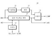
도 3a는 상술한 도 2의 어드레스 입력회로(10)의 일 실시예를 나타내는 블록도이다. 도 3a를 참조하면, 본 발명의 어드레스 입력회로(10)는 프로그램 시작 명령 후 최초 입력되는 어드레스(ADD)를 저장하는 초기 어드레스 래치(11), 입력되는 어드레스(ADD)가 순차적으로 실시간 래치되는 입력 어드레스 래치(12), 실시간 입력되는 현재 어드레스와 초기 어드레스를 비교하고 그 결과를 출력하는 비교기(13), 그리고 버퍼로의 데이터 로드 수를 카운트하여 상태 데이터(B_L_Count)로 공급하기 위한 카운터(14)를 포함한다. 이러한 구성의 어드레스 입력회로(10)는 외부 어드레스(ADD)를 쓰기 인에이블 신호(nWE)에 동기하여 입력받아 상태 데이터(B_L_Count)와 어드레스(B_ADD, F_ADD), 어드레스 비교신호(A_COMP)를 공급할 수 있다.FIG. 3A is a block diagram illustrating an embodiment of the
초기 어드레스 래치(11)는 프로그램 시작(Program Start) 명령의 입력 이후 최초로 입력되는 어드레스를 저장하는 래치 회로이다. 초기 어드레스는 하나의 버퍼링 단위(예를 들면 128워드 크기의 프로그램 데이터)의 데이터 중 최초로 멀티 버퍼(20)에 로드되는 데이터와 대응하는 어드레스이다. 초기 어드레스는 매 프로그램 시작(Program Start) 명령어가 입력될 때마다 상술한 초기 어드레스 래치(11)에 래치되고, 멀티 버퍼(20)에 로드된 데이터가 셀 어레이(50)로 프로그램될 때까지 유지된다. 도면에서 래치를 제어하는 신호의 표기는 생략되어 있으나, 초기 어드레스 래치(11)는 프로그램 시작(Program Start)명령에 동기되어 최초로 입력되는 어드레스가 래치되도록 설정될 수 있다.The
입력 어드레스 래치(12)는 현재 입력되는 어드레스가 일시 저장되는 래치 회로이다. 쓰기 인에이블 신호(nWE)가 토글될 때마다 실시간 입력되는 어드레스(ADD)가 입력 어드레스 래치(12)에 저장된다.The
비교기(13)는 입력 어드레스들을 비교하여 어드레스 비교신호(A_COMP)를 생성한다. 그리고 어드레스 비교신호(A_COMP)는 상태 데이터(S_Data)가 출력될 것인지 혹은 리드 데이터(R_Data)가 출력할 것인지의 여부가 결정되도록 출력 버퍼 제어회로(40)로 전달된다. 비교기(13)는 초기 어드레스와 실시간으로 입력되는 현재 어드레스를 비교하여 동일한 버퍼링 단위의 어드레스인지, 또는 초기 어드레스와 다른 메모리 뱅크나 섹터들을 지정하는 것인지를 검출하는 회로이다. 만일 초기 어드레스 래치(12)에 저장된 초기 어드레스와 입력 어드레스 래치(13)에 일시 저장된 현재의 실시간 입력 어드레스가 동일한 버퍼링 단위 어드레스라면 어드레스 비교신호(A_COMP)는 'HIGH'가 된다. 반면에, 로드되는 데이터들의 어드레스와 다른 버퍼링 단위 어드레스가 입력되면 'LOW'로 천이 되도록 설정된다. 이러한 비교기(13)의 동작을 위해서는 초기 어드레스와 현재 입력 어드레스 간의 비교연산이 이루어지는 비트 수의 설정에 의해 구현가능하다. 만일 128워드가 멀티 버퍼(20)의 버퍼링 단위라면, 전체 어드레스 비트 중 버퍼 어드레스(B_ADD)에 해당하는 하위 7비트는 비교 연산에서 제외하고, 뱅크나 섹터, 블록들을 지시하는 상위 어드레스만을 비교하여 현재 입력되는 어드레스가 최초 어드레스와 동일한 버퍼링 단위인지를 검출할 수 있다. 표 2의 예를 통해 설명하면, 아래 표 2는 일반적인 노어 플래시 메모리의 어드레스 구성을 본 발명의 실시예를 설명하기 위해 간략히 구분하였다.The
표 2의 구분에 의하면, 상위 어드레스는 셀 어레이(50)의 뱅크, 블록, 섹터 등의 어드레스를 지시하는 비트들이라 가정하고, 하위 어드레스는 그 이하의 어드레스에 해당한다. 하위 어드레스는 또한 본 발명의 멀티 버퍼(20)가 128워드 크기인 경우 멀티 버퍼(20)에 로드되는 버퍼 어드레스(B_ADD)로 사용될 수 있다. 7비트 크기의 어드레스로 멀티 버퍼(20)내의 각각의 버퍼가 모두 지정될 수 있다. 이러한 어드레스 구조에 의거하여 본 발명의 비교기(13)를 설명하면, 본 발명의 비교기(13)는 초기 어드레스 래치(11)와 입력 어드레스 래치(12)로부터 상위 어드레스를 입력받아 비교하게 된다. 상위 어드레스가 다른 비트 값을 갖는 경우 어드레스 비교신호(A_COMP)는 로우(LOW)로 출력되고, 동일한 상위 어드레스라면 하이(HIGH)로 출력된다. 현재 입력되는 어드레스가 동일한 버퍼링 단위 어드레스인지의 여부를 검출하기 위한 비교기(13)의 설정 방법은 상술한 방법에만 국한되지 않음은 이 분야에서 통상의 지식을 습득한 자들에게는 자명하다.According to the division of Table 2, it is assumed that the upper address is bits indicating the address of the bank, block, sector, etc. of the
카운터(14)는 입력되는 멀티 버퍼(20)로 로드되는 데이터의 수를 카운트하여 상태정보로 제공한다. 특히 본 발명의 카운터(14)는 쓰기 인에이블 신호(nWE)에 동기되어 입력되는 데이터의 수(B_L_Count)를 카운트하여 상태 데이터 버퍼(100)로 전송된다.The counter 14 counts the number of data loaded into the multi-buffer 20 to be input and provides the status information. In particular, the
이상의 설명으로 알 수 있듯이, 어드레스 입력회로(10)는 초기 어드레스와 현재 입력되는 어드레스를 비교하여 출력 버퍼 제어회로(40)가 상태 데이터(S_Data)를 출력할 것인지 혹은 리드 데이터(R_Data)를 출력할 것인지 판단하는 근거가 되는 어드레스 비교신호(A_COMP)를 생성한다. 또한, 어드레스 입력회로(10)는 현재 멀티 버퍼(20)에 로드되는 데이터의 수를 나타내는 로드 카운트 수(B_L_Count)를 상태 데이터 버퍼(100)로 제공한다.As can be seen from the above description, the
도 3b는 상술한 본 발명의 제 1 실시예에 포함된 어드레스 입력회로(10)의 다른 실시예를 설명하는 블록도이다. 여기서, 앞서 도시된 도 3a에서와 동일한 참조부호는 동일한 기능을 하는 동일한 부재를 가리킨다. 도 3b에 도시된 어드레스 입력회로(10)는 초기 어드레스 래치(11)가 지연 회로(15)와 래치(16)로 대체되었다는 점을 제외하면 도 3a에 도시된 것과 실질적으로 동일하다.3B is a block diagram for explaining another embodiment of the
지연회로(15)는 입력되는 어드레스를 하나의 클록만큼 지연하는 회로이다. 동기식 모드에서는 외부에서 입력되는 클록에 의해 입력 어드레스가 지연되고, 비동기식 모드에서는 쓰기 인에이블 신호(nWE)의 토글(Toggle) 동작에 동기하여 입력 어드레스가 지연될 것이다. 본 발명의 멀티 버퍼(20)로의 데이터 로드 단위가 워드 단위라 가정하면, 현재 입력되는 어드레스 이전의 어드레스가 래치(12)에 저장되도록 지연회로(15)가 설정될 것이다. 래치(16)는 상술한 지연회로(15)에 의해 지연된 어드레스가 일시 저장되는 래치 회로이다.The
이상의 구성은 통한 어드레스 입력회로(10)는 현재 입력되는 어드레스와 바로 이전에 입력되는 어드레스를 비교하여 출력 버퍼 제어회로(40)가 상태 데이터(S_Data)를 출력할 것인지 혹은 리드 데이터(R_Data)를 출력할 것인지 판단하는 근거가 되는 어드레스 비교신호(A_COMP)를 생성한다. 또한, 어드레스 입력회로(10)는 멀티 버퍼(20)로 프로그램 데이터를 로드하기 위한 버퍼 어드레스(B_ADD)와 현재 멀티 버퍼(20)에 로드되는 데이터의 수를 나타내는 로드 카운트 수(B_L_Count)를 생성하여 상태정보로 제공할 수 있다.According to the above configuration, the
도 4는 본 발명의 제 2 실시예를 보여주는 블록도이다. 여기서, 앞서 도시된 도 2에서와 동일한 참조부호는 동일한 기능을 하는 동일한 부재를 가리킨다. 도 2에 도시된 어드레스 입력회로(10)로부터 로드 데이터 수(B_L_Count)가 생성되지 안는 점과 멀티 버퍼(20)의 로드 데이터(B_L_Data)가 상태 데이터로 출력된다는 점을 제외하면 도 2에 도시된 것과 실질적으로 동일하다.4 is a block diagram showing a second embodiment of the present invention. Here, the same reference numerals as in FIG. 2 shown above indicate the same members having the same function. 2, except that the load data number B_L_Count is not generated from the
어드레스 입력회로(10)는 어드레스 비교신호(A_COMP)와 어드레스(F_ADD, B_ADD)를 각 구성요소로 공급한다. 그러나 버퍼에 로드된 데이터의 수를 카운트하기 위한 수단은 구비하고 있지 않은 어드레스 입력회로(10)이다. 또는 카운터를 포함하되 그 출력을 상태 데이터로 공급하지 않도록 설정될 수 있다.The
제 2 실시예에서 개시되는 멀티 버퍼(20)는 쓰기 인에이블 신호(nWE)의 토글시에는 프로그램될 데이터(PD)가 버퍼 어드레스(B_ADD)가 지정하는 각 버퍼들로 로드된다. 그러나 쓰기 인에이블 신호(nWE)가 하이로 비활성화된 이후에 입력되는 버퍼 어드레스(B_ADD)에 대해서는, 해당하는 어드레스에 로드된 데이터(B_L_Data)를 상태 데이터 버퍼(100)로 출력하도록 설정된다.In the multi-buffer 20 disclosed in the second embodiment, when the write enable signal nWE is toggled, the data PD to be programmed is loaded into the respective buffers designated by the buffer address B_ADD. However, for the buffer address B_ADD input after the write enable signal nWE is deactivated high, the data B_L_Data loaded at the corresponding address is output to the
도 4에 도시된 본 발명의 제 2 실시예에 따르면 본 발명의 메모리 장치는 프로그램 시작 명령어의 입력 이후 멀티 버퍼(20)로 프로그램 데이터를 로드하는 중에 쓰기 인에이블 신호(nWE)를 하이로 유지하면서 출력 인에이블 신호(nOE)를 토클하게 되면 멀티 버퍼(20)에 로드된 데이터를 외부로 출력할 수 있다.According to the second embodiment of the present invention shown in FIG. 4, the memory device of the present invention maintains the write enable signal nWE high while loading program data into the multi-buffer 20 after input of a program start command. When the output enable signal nOE is toggled, the data loaded in the
도 5a는 상술한 도 4의 어드레스 입력회로(10)의 일 실시예를 나타내는 블록도이다. 여기서, 앞서 도시된 도 3a에서와 동일한 참조부호는 동일한 기능을 하는 동일한 부재를 가리킨다. 도 5a에 도시된 어드레스 입력회로(10)는 멀티 버퍼(20)의 데이터 로드 수(B_L_Count)를 상태 데이터 버퍼(100)로 공급하지 않는다는 점을 제외하면 도 3a의 어드레스 입력회로(10)와 실직적으로 동일하다.FIG. 5A is a block diagram illustrating an embodiment of the
도 5b는 상술한 도 4의 어드레스 입력회로(10)의 다른 실시예를 나타내는 블록도이다. 도 5b에 도시된 어드레스 입력회로(10)는 멀티 버퍼(20)의 데이터 로드 수(B_L_Count)를 카운트하여 상태 데이터 버퍼(100)로 공급하는 카운터(14)를 포함하지 않는다는 점을 제외하면 도 3b의 어드레스 입력회로(10)와 실질적으로 동일하다.FIG. 5B is a block diagram illustrating another embodiment of the
이상의 본 발명의 제 2 실시예는 도 4와 도 5a, 도 5b의 블록도를 통해서 설명되었다. 제 2 실시예에 따른 본 발명은 프로그램 시작 명령(Program Start) 이후 멀티 버퍼(20)로 프로그램될 데이터의 로드 중에 출력 쓰기 인에이블 신호(nWE)의 토글을 중지하고, 출력 인에이블 신호(nOE)를 로우로 활성화하여 멀티 버퍼(20)에 로드된 데이터(B_L_Data)를 외부로 출력하여 확인할 수 있다. 이러한 동작은 멀티 버퍼(20)로의 로드 데이터의 에러 유무를 확인하는데 이용할 수 있어, 메모리 장치의 신뢰성 향상시킬 수 있다.The second embodiment of the present invention has been described with reference to the block diagrams of FIGS. 4, 5A, and 5B. The present invention according to the second embodiment stops the toggle of the output write enable signal nWE during the loading of data to be programmed into the multi-buffer 20 after the program start command, and the output enable signal nOE. By activating low, the data B_L_Data loaded in the multi-buffer 20 can be output to the outside and checked. This operation can be used to confirm the presence or absence of an error of load data to the multi-buffer 20, thereby improving the reliability of the memory device.
도 6은 본 발명에 따른 플래시 메모리 장치의 동작을 설명하기 위한 타이밍도이다. 이하 상술한 도면들에 의거하여 본 발명에 따른 플래시 메모리 장치의 동작이 상세히 설명될 것이다.6 is a timing diagram illustrating an operation of a flash memory device according to the present invention. Hereinafter, the operation of the flash memory device according to the present invention will be described in detail with reference to the above-described drawings.
먼저, 멀티 버퍼(20)로의 데이터 로드를 위해서 프로그램 시작 명령(또는 버퍼 로드 시작 명령)이 칩 인에이블 신호(nCE)가 'LOW'로 활성화된 상태에서 쓰기 인에이블 신호(nWE)의 토글에 동기되어 입력된다(tC). 프로그램 시작 명령어(CMD1)(도면에서는 D0~D1로 표기됨)는 쓰기 인에이블 신호(nWE) 2-사이클 동안 각각 어드레스(A0~A1)와 I/O(데이터 입출력) 핀을 통해서 입력될 것이다. 또한, 상술한 도면에서는 두 클록 동안 프로그램 시작 명령(CMD1)이 입력되는 것으로 나타나 있으나 3 클록이나 그 이상으로도 설정될 수 있음은 이 분야에서 통상의 지식을 습득한 자들에게는 자명하다.First, a program start command (or a buffer load start command) is synchronized with a toggle of the write enable signal nWE while the chip enable signal nCE is activated to 'LOW' for data loading into the multi-buffer 20. Inputted (tC). The program start command CMD1 (indicated by D0 to D1 in the drawing) will be input via the address A0 to A1 and I / O (data input / output) pins for the write enable signal nWE two cycles, respectively. In addition, in the above-described drawings, the program start command CMD1 is input for two clocks, but it may be set to three clocks or more, which is obvious to those skilled in the art.
프로그램 시작 명령어(CMD1)의 입력 이후, 멀티 버퍼(20)로의 로드 명령의 유무를 나타내는 버퍼 로드 스타트 신호(B_L_Start)는 'HIGH'로 천이하게 된다. 이것은 멀티 버퍼(20)로의 데이터 로드가 시작되었음을 의미한다. 또한, 순차적으로 프로그램 어드레스(PA)들과 그에 대응되는 프로그램 데이터(PD)들이 입력될 것이다. 한 번의 쓰기 인에이블 신호(nWE)의 토글 동안 하나의 워드가 입력되는 경우, 128 워드가 로드되는 멀티 버퍼(20)의 경우 128번의 쓰기 인에이블 신호(nWE)의 토글을 통해서 프로그램 데이터(PD)와 프로그램 어드레스(PA)가 입력될 것이다. 멀티 버퍼(20)로의 로드가 완료되고 프로그램 확정(Confirm) 명령(CMD2)이 입력된 이후부터는 멀티 버퍼(20)에 로드된 데이터가 입력된 어드레스에 해당하는 메모리 셀로 프로그램된다. 이상의 동작은 멀티 버퍼(20)로의 로드 동작중에 출력 인에이블 신호(nOE)를 토글하지 않았을 경우에 해당되는 정상적인 동작에 대한 설명이다.After the program start command CMD1 is input, the buffer load start signal B_L_Start indicating whether there is a load command to the
이하에서는 본 발명에 따른 멀티 버퍼(20)로의 로드가 시작된 이후부터 멀티 버퍼(20)로의 로드 상태를 확인하기 위한 동작을 설명하기로 한다. 멀티 버퍼(20)로의 데이터 로드 동작중에 상태 데이터(S_Data)를 확인하기 위해서는 쓰기 인에이블 신호(nWE)를 'HIGH'로 유지하여 데이터의 입력을 중지하고, 출력 인에이블 신호(nOE)를 'LOW'로 토글(Toggle)한다. 이때 입력되는 어드레스(SA0)는 멀티 버퍼(20)로 프로그램 데이터의 로드를 위해 입력되던 프로그램 어드레스(PA) 중의 하나를 입력하게 된다. 도면에서 어드레스(SA0)는 이전에 입력되는 프로그램 어드레스(PA)들 중 최종 입력된 어드레스에 해당한다. 이 경우, 출력 버퍼 제어회로(40)의 출력은 상술한 표 1의 조건을 고려할 때 어드레스 비교신호(A_COMP)가 'HIGH'가 되고, 데이터 로드가 종료되지 않았기 때문에 출력 버퍼 제어신호 (SDO_EN)이 'HIGH'로 천이된다. 출력 버퍼 제어신호(SDO_EN)가 하이로 활성화됨에 따라, 상태 데이터 버퍼(100)에 실시간으로 저장된 상태 데이터는 출력 버퍼(90)를 통해서 외부로 출력된다. 이때, 상태 데이터(SD0)는 도 2에서 도시된 본 발명의 제 1 실시예에 따를 경우, 프로그램 시작 명령어(CMD1)의 입력 여부(B_L_Start), 멀티 버퍼(20)에 로드된 데이터 수(B_L_Count)의 정보를 포함하는 데이터가 될 것이다. 또는 도 4와 같은 제 2 실시예의 경우라면, 상태 데이터(SD0)는 로드된 데이터 수(B_L_Count)가 아닌 어드레스(SA0)에 대응하는 멀티 버퍼(20)로 로드된 버퍼 로드 데이터(B_L_Data)를 포함할 것이다. 두 번째의 출력 인에이블 신호(nOE)의 토글에서도 상술한 동작과 동일한 상태 데이터가 출력될 것이다.Hereinafter, an operation for confirming the load state to the multi-buffer 20 after the load to the multi-buffer 20 according to the present invention starts will be described. To check the status data S_Data during the data load operation to the multi-buffer 20, the write enable signal nWE is maintained at 'HIGH' to stop data input and the output enable signal nOE is set to 'LOW'. Toggle with ' In this case, the input address SA0 is input to one of the program addresses PA input to load the program data into the multi-buffer 20. In the drawing, the address SA0 corresponds to the last input address among the previously input program addresses PA. In this case, since the address comparison signal A_COMP becomes 'HIGH' when the output
반면에, 멀티 버퍼(20)로의 데이터 로드 중에 현재의 버퍼링 단위의 어드레스들과 관련이 없는 다른 메모리 뱅크나 섹터의 저장된 데이터를 확인하고자 할 경우를 설명하기로 한다. 도면에서는 출력 인에이블 신호(nOE)의 세 번째 토글에 해당된다. 이 경우에는 상태 데이터를 확인하는 절차와 방법은 같지만 입력되는 어드레스에 차이가 있다. 이 경우 쓰기 인에이블 신호(nWE)를 'HIGH'로 유지하면서 다른 뱅크나 섹터를 지시하는 상위 비트를 가지는 어드레스(RA1)을 입력하고 출력 인에이블 신호(nOE)를 'LOW'로 토글하면 된다. 이때 예상되는 바와 같이 어드레스의 비교신호(A_COMP)가 'LOW'로 천이되고, 출력 버퍼 제어회로(40)는 출력 버퍼 제어 신호(RDO_EN)를 'HIGH'로 활성화시킨다. 출력 버퍼(90)는 활성화된 제어 신호(RDO_EN)에 응답하여 리드 데이터 버퍼(80)로부터의 독출된 데이터(RD1)를 외부로 출력한다. 상술한 독출 데이터(RD1)는 어드레스(RA1)가 지시하는 셀 어레이로부터 독출한 데이터이다.On the contrary, a case in which the stored data of another memory bank or sector that is not related to the addresses of the current buffering unit during the data loading to the multi-buffer 20 is to be described will be described. In the figure, it corresponds to the third toggle of the output enable signal nOE. In this case, the procedure and method of checking the status data are the same, but there are differences in the input addresses. In this case, while maintaining the write enable signal nWE as 'HIGH', an address RA1 having an upper bit indicating another bank or sector may be input, and the output enable signal nOE may be toggled to 'LOW'. As expected, the comparison signal A_COMP of the address transitions to 'LOW', and the output
더불어, 버퍼(20)로의 모든 데이터 로드가 종료되고, 프로그램 확정(Program Confirm) 명령어(CMD2 : A3와 D3로 입력)의 입력 이후(tP)에는 멀티 버퍼(20)에 로드된 데이터가 셀 어레이로의 프로그램 중임을 나타내는 상태 데이터인 프로그램 비지 신호(P_Busy)가 출력될 수 있다. 예를 들면 도 4의 네 번째 출력 인에이블 신호(nOE)의 토글이 이에 해당된다. 도시한 바와 같이, 프로그램 비지 신호(P_Busy)가 하이가 될 때, 출력 버퍼 제어 회로(40)는 프로그램 비지 신호(P_Busy)에 응답하여 출력 버퍼 제어 신호(SDO_EN)를 하이로 활성화시킨다. 이는 상태 데이터 버퍼(100)에 저장된 데이터 즉, 프로그램 비지 신호(P_Busy)의 상태를 나타내는 데이터가 출력 버퍼(90)를 통해서 출력되게 한다. 이상에서 프로그램 확정(Program Confirm) 명령(CMD2)을 외부에서 입력하는 것으로 설명하였으나, 프로그램 확정(Program Confirm) 명령은 프로그램 데이터의 카운트 수로도 제어가 가능하다. 이는 외부의 명령어 입력 없이 멀티 버퍼(20)에 로드가 완료되면 자동적으로 셀 어레이로 프로그램되도록 설정할 수 있다.In addition, all data loading to the
본 발명에 따른 메모리 장치는 멀티 버퍼(20)로의 데이터 로드중에 로드되는 멀티 버퍼(20)의 제반 상태 데이터를 출력 받을 수 있는 장치와 방법을 제공한다. 이를 통해서 본 발명은 데이터 로드 동작중에 상태 데이터 버퍼(100)를 통해서 실시간으로 출력 받는 상태정보를 기초로 보다 신뢰성 있는 버퍼 로드 동작을 구성할 수 있다.The memory device according to the present invention provides an apparatus and a method capable of outputting various state data of the multi-buffer 20 loaded during data loading into the multi-buffer 20. Through this, the present invention can configure a more reliable buffer load operation based on the state information received in real time through the
한편, 본 발명의 상세한 설명에서는 구체적인 실시예에 관하여 설명하였으나, 본 발명의 범위에서 벗어나지 않는 한도 내에서 여러 가지 변형이 가능함은 물론이다. 그러므로 본 발명의 범위는 상술한 실시예에 국한되어 정해져서는 안되며 후술하는 특허청구범위뿐만 아니라 이 발명의 특허청구범위와 균등한 것들에 의해 정해져야 한다.On the other hand, in the detailed description of the present invention has been described with respect to specific embodiments, various modifications are of course possible without departing from the scope of the invention. Therefore, the scope of the present invention should not be limited to the above-described embodiments, but should be defined by the equivalents of the claims of the present invention as well as the following claims.
상술한 바와 같이 본 발명은 버퍼로의 프로그램 데이터의 로드 중에 데이터 로드 상태를 확인할 수 있는 장치와 방법을 제공하여 프로그램 동작의 신뢰성을 개선할 수 있다.As described above, the present invention can improve the reliability of program operation by providing an apparatus and a method capable of checking a data load state while loading program data into a buffer.
Claims (32)
Translated fromKoreanPriority Applications (3)
| Application Number | Priority Date | Filing Date | Title |
|---|---|---|---|
| KR1020050079453AKR100729358B1 (en) | 2005-08-29 | 2005-08-29 | Flash memory device with multi-buffer program scheme |
| DE102006041968ADE102006041968B4 (en) | 2005-08-29 | 2006-08-28 | Memory element and method for programming a memory element |
| US11/510,762US20070050537A1 (en) | 2005-08-29 | 2006-08-28 | Flash memory device including a multi buffer program scheme |
Applications Claiming Priority (1)
| Application Number | Priority Date | Filing Date | Title |
|---|---|---|---|
| KR1020050079453AKR100729358B1 (en) | 2005-08-29 | 2005-08-29 | Flash memory device with multi-buffer program scheme |
Publications (2)
| Publication Number | Publication Date |
|---|---|
| KR20070027073A KR20070027073A (en) | 2007-03-09 |
| KR100729358B1true KR100729358B1 (en) | 2007-06-15 |
Family
ID=37805690
Family Applications (1)
| Application Number | Title | Priority Date | Filing Date |
|---|---|---|---|
| KR1020050079453AExpired - Fee RelatedKR100729358B1 (en) | 2005-08-29 | 2005-08-29 | Flash memory device with multi-buffer program scheme |
Country Status (3)
| Country | Link |
|---|---|
| US (1) | US20070050537A1 (en) |
| KR (1) | KR100729358B1 (en) |
| DE (1) | DE102006041968B4 (en) |
Cited By (1)
| Publication number | Priority date | Publication date | Assignee | Title |
|---|---|---|---|---|
| KR101401806B1 (en) | 2013-01-30 | 2014-05-29 | 한양대학교 산학협력단 | Apparatus and method for control multi-channel non-volatile memory using shared buffer |
Families Citing this family (1)
| Publication number | Priority date | Publication date | Assignee | Title |
|---|---|---|---|---|
| JP2008152464A (en)* | 2006-12-15 | 2008-07-03 | Toshiba Corp | Storage device |
Citations (4)
| Publication number | Priority date | Publication date | Assignee | Title |
|---|---|---|---|---|
| KR970068162A (en)* | 1996-03-08 | 1997-10-13 | 김주용 | A data output buffer selector of a semiconductor memory device |
| JP2004085317A (en)* | 2002-08-26 | 2004-03-18 | Sumitomo Rubber Ind Ltd | Friction characteristic measuring apparatus |
| KR20040085317A (en)* | 2003-03-31 | 2004-10-08 | 삼성전자주식회사 | Apparatus and method for buffering data |
| JP2005149575A (en) | 2003-11-12 | 2005-06-09 | Ricoh Co Ltd | Semiconductor memory device |
Family Cites Families (6)
| Publication number | Priority date | Publication date | Assignee | Title |
|---|---|---|---|---|
| EP0404013B1 (en)* | 1989-06-19 | 1995-12-13 | Nec Corporation | Semiconductor memory device with an improved write control circuit |
| US5519847A (en)* | 1993-06-30 | 1996-05-21 | Intel Corporation | Method of pipelining sequential writes in a flash memory |
| JP2001052495A (en)* | 1999-06-03 | 2001-02-23 | Toshiba Corp | Semiconductor memory |
| US6721546B1 (en)* | 2001-02-27 | 2004-04-13 | Point Six Wireless, Llc | Wireless communication system including a unique data transmission device |
| KR100504696B1 (en)* | 2003-02-26 | 2005-08-03 | 삼성전자주식회사 | Nand-type flash memory device having array of status cells for storing block erase/program information |
| KR100849296B1 (en)* | 2003-06-13 | 2008-07-29 | 삼성전자주식회사 | Apparatus and method for initiating an auxiliary control unit in a system having a main controller and an auxiliary control unit |
- 2005
- 2005-08-29KRKR1020050079453Apatent/KR100729358B1/ennot_activeExpired - Fee Related
- 2006
- 2006-08-28DEDE102006041968Apatent/DE102006041968B4/ennot_activeExpired - Fee Related
- 2006-08-28USUS11/510,762patent/US20070050537A1/ennot_activeAbandoned
Patent Citations (4)
| Publication number | Priority date | Publication date | Assignee | Title |
|---|---|---|---|---|
| KR970068162A (en)* | 1996-03-08 | 1997-10-13 | 김주용 | A data output buffer selector of a semiconductor memory device |
| JP2004085317A (en)* | 2002-08-26 | 2004-03-18 | Sumitomo Rubber Ind Ltd | Friction characteristic measuring apparatus |
| KR20040085317A (en)* | 2003-03-31 | 2004-10-08 | 삼성전자주식회사 | Apparatus and method for buffering data |
| JP2005149575A (en) | 2003-11-12 | 2005-06-09 | Ricoh Co Ltd | Semiconductor memory device |
Non-Patent Citations (1)
| Title |
|---|
| 공개 특허 제2004-85317호 |
Cited By (1)
| Publication number | Priority date | Publication date | Assignee | Title |
|---|---|---|---|---|
| KR101401806B1 (en) | 2013-01-30 | 2014-05-29 | 한양대학교 산학협력단 | Apparatus and method for control multi-channel non-volatile memory using shared buffer |
Also Published As
| Publication number | Publication date |
|---|---|
| KR20070027073A (en) | 2007-03-09 |
| DE102006041968B4 (en) | 2010-08-05 |
| DE102006041968A1 (en) | 2007-05-10 |
| US20070050537A1 (en) | 2007-03-01 |
Similar Documents
| Publication | Publication Date | Title |
|---|---|---|
| US11600323B2 (en) | Non-volatile memory device with concurrent bank operations | |
| US7599222B2 (en) | Semiconductor memory device using pipelined-buffer programming and related method | |
| EP2306461A2 (en) | Memory with output control | |
| US7873753B2 (en) | Memory subsystem capable of accessing a plurality of memory bank identifications and method thereof | |
| JP5101123B2 (en) | Burst read circuit and burst data output method for semiconductor memory device | |
| US8687423B2 (en) | Nonvolatile memory device and method of operating the same | |
| KR100729358B1 (en) | Flash memory device with multi-buffer program scheme | |
| US20230253036A1 (en) | Non-volatile memory device with concurrent bank operations | |
| US8897048B2 (en) | Semiconductor memory device and programming method thereof | |
| JP2021152779A (en) | Semiconductor memory device | |
| JP2004206850A (en) | Semiconductor storage device | |
| KR100560800B1 (en) | Nonvolatile Memory Device and Its Program Speed Improvement Method | |
| US7477569B2 (en) | Semiconductor memory device capable of performing page mode operation | |
| KR20100009476A (en) | Circuit of inputting a data and non volatile memory device having the same |
Legal Events
| Date | Code | Title | Description |
|---|---|---|---|
| A201 | Request for examination | ||
| PA0109 | Patent application | St.27 status event code:A-0-1-A10-A12-nap-PA0109 | |
| PA0201 | Request for examination | St.27 status event code:A-1-2-D10-D11-exm-PA0201 | |
| D13-X000 | Search requested | St.27 status event code:A-1-2-D10-D13-srh-X000 | |
| D14-X000 | Search report completed | St.27 status event code:A-1-2-D10-D14-srh-X000 | |
| E902 | Notification of reason for refusal | ||
| PE0902 | Notice of grounds for rejection | St.27 status event code:A-1-2-D10-D21-exm-PE0902 | |
| T11-X000 | Administrative time limit extension requested | St.27 status event code:U-3-3-T10-T11-oth-X000 | |
| P11-X000 | Amendment of application requested | St.27 status event code:A-2-2-P10-P11-nap-X000 | |
| P13-X000 | Application amended | St.27 status event code:A-2-2-P10-P13-nap-X000 | |
| PG1501 | Laying open of application | St.27 status event code:A-1-1-Q10-Q12-nap-PG1501 | |
| E701 | Decision to grant or registration of patent right | ||
| PE0701 | Decision of registration | St.27 status event code:A-1-2-D10-D22-exm-PE0701 | |
| GRNT | Written decision to grant | ||
| PR0701 | Registration of establishment | St.27 status event code:A-2-4-F10-F11-exm-PR0701 | |
| PR1002 | Payment of registration fee | St.27 status event code:A-2-2-U10-U11-oth-PR1002 Fee payment year number:1 | |
| PG1601 | Publication of registration | St.27 status event code:A-4-4-Q10-Q13-nap-PG1601 | |
| LAPS | Lapse due to unpaid annual fee | ||
| PC1903 | Unpaid annual fee | St.27 status event code:A-4-4-U10-U13-oth-PC1903 Not in force date:20100612 Payment event data comment text:Termination Category : DEFAULT_OF_REGISTRATION_FEE | |
| PC1903 | Unpaid annual fee | St.27 status event code:N-4-6-H10-H13-oth-PC1903 Ip right cessation event data comment text:Termination Category : DEFAULT_OF_REGISTRATION_FEE Not in force date:20100612 | |
| R18-X000 | Changes to party contact information recorded | St.27 status event code:A-5-5-R10-R18-oth-X000 |