KR100729256B1 - Photoresist composition, method for forming a photoresist pattern and method for forming a protection layer of a semiconductor device using the photoresist composition - Google Patents
Photoresist composition, method for forming a photoresist pattern and method for forming a protection layer of a semiconductor device using the photoresist compositionDownload PDFInfo
- Publication number
- KR100729256B1 KR100729256B1KR1020050130524AKR20050130524AKR100729256B1KR 100729256 B1KR100729256 B1KR 100729256B1KR 1020050130524 AKR1020050130524 AKR 1020050130524AKR 20050130524 AKR20050130524 AKR 20050130524AKR 100729256 B1KR100729256 B1KR 100729256B1
- Authority
- KR
- South Korea
- Prior art keywords
- compound
- photoresist
- photoresist composition
- formula
- protective film
- Prior art date
- Legal status (The legal status is an assumption and is not a legal conclusion. Google has not performed a legal analysis and makes no representation as to the accuracy of the status listed.)
- Expired - Fee Related
Links
Images


Classifications
- G—PHYSICS
- G03—PHOTOGRAPHY; CINEMATOGRAPHY; ANALOGOUS TECHNIQUES USING WAVES OTHER THAN OPTICAL WAVES; ELECTROGRAPHY; HOLOGRAPHY
- G03F—PHOTOMECHANICAL PRODUCTION OF TEXTURED OR PATTERNED SURFACES, e.g. FOR PRINTING, FOR PROCESSING OF SEMICONDUCTOR DEVICES; MATERIALS THEREFOR; ORIGINALS THEREFOR; APPARATUS SPECIALLY ADAPTED THEREFOR
- G03F7/00—Photomechanical, e.g. photolithographic, production of textured or patterned surfaces, e.g. printing surfaces; Materials therefor, e.g. comprising photoresists; Apparatus specially adapted therefor
- G03F7/004—Photosensitive materials
- G03F7/022—Quinonediazides
- G03F7/023—Macromolecular quinonediazides; Macromolecular additives, e.g. binders
- G03F7/0233—Macromolecular quinonediazides; Macromolecular additives, e.g. binders characterised by the polymeric binders or the macromolecular additives other than the macromolecular quinonediazides
Landscapes
- Physics & Mathematics (AREA)
- Spectroscopy & Molecular Physics (AREA)
- General Physics & Mathematics (AREA)
- Materials For Photolithography (AREA)
Abstract
Translated fromKoreanDescription
Translated fromKorean도 1 내지 도 3은 본 발명의 일 실시예에 따른 포토레지스트 패턴의 형성방법을 설명하기 위한 단면도들이다.1 to 3 are cross-sectional views illustrating a method of forming a photoresist pattern according to an embodiment of the present invention.
도 4 내지 도 6은 본 발명의 일 실시예에 따른 반도체 소자의 보호막 형성방법을 설명하기 위한 단면도들이다.4 to 6 are cross-sectional views illustrating a method of forming a protective film of a semiconductor device according to an embodiment of the present invention.
도 7 내지 도 11은 본 발명의 일 실시예에 따른 반도체 소자의 보호막 형성방법을 설명하기 위한 단면도들이다.7 to 11 are cross-sectional views illustrating a method of forming a protective film of a semiconductor device according to an embodiment of the present invention.
도 12 및 도 13은 실시예 및 비교에에 따라 제조된 포토레지스트 조성물을 사용하여 형성된 포토레지스트 막을 현상한 후의 결과를 나타내는 전자현미경 사진들이다.12 and 13 are electron micrographs showing the results after the development of the photoresist film formed using the photoresist composition prepared according to Examples and Comparative.
* 도면의 주요부분에 대한 부호의 설명 *Explanation of symbols on the main parts of the drawings
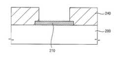
100: 대상물200, 300: 기판100:
110, 120: 포토레지스트막130: 마스크110 and 120: photoresist film 130: mask
140: 포토레지스트 패턴210: 패드140: photoresist pattern 210: pad
220, 230: 예비 보호막240: 보호막220, 230: preliminary protective film 240: protective film
310: 본딩 패드320: 제1 보호막310: bonding pad 320: first protective film
330, 340: 제2 보호막350: 제2 보호막 패턴330 and 340: second protective film 350: second protective film pattern
360: 제1 보호막 패턴360: first protective film pattern
본 발명은 포토레지스트 조성물, 이를 이용한 포토레지스트 패턴의 형성방법 및 보호막의 형성 방법에 관한 것이다. 보다 상세하게는 반도체 소자 완성 후, 보호막 형성 단계에서 사용할 수 있는 포토레지스트 조성물, 이를 이용한 포토레지스트 패턴의 형성방법 및 반도체 소자의 보호막 형성 방법에 관한 것이다.The present invention relates to a photoresist composition, a method of forming a photoresist pattern and a method of forming a protective film using the same. More particularly, the present invention relates to a photoresist composition which can be used in a protective film forming step after completion of a semiconductor device, a method of forming a photoresist pattern using the same, and a method of forming a protective film of a semiconductor device.
근래에 컴퓨터와 같은 정보 매체의 급속한 보급에 따라 반도체 메모리 소자도 비약적으로 발전하고 있다. 그 기능 면에 있어서 반도체 메모리 소자는 고속으로 동작하는 동시에 대용량의 저장능력을 가질 것이 요구된다. 이러한 요구에 부응하여 반도체 제조 기술은 소자의 집적도, 신뢰성 및 응답속도 등을 향상시키는 방향으로 발전되어 왔다.In recent years, with the rapid spread of information media such as computers, semiconductor memory devices are also rapidly developing. In terms of its function, the semiconductor memory device is required to operate at a high speed and to have a large storage capacity. In response to these demands, semiconductor manufacturing techniques have been developed to improve device integration, reliability, and response speed.
반도체 메모리 장치는 크게 휘발성과 비휘발성 메모리 장치로 분류된다. 휘발성 메모리 장치에 속하는 에스램(static random access memory; SRAM)이나 디램(dynamic random access memory; DRAM)은 파워(power)가 오프(off)되면 데이터가 지워지는 특성이 있다. 반면, 비휘발성 메모리 장치에 속하는 롬(read only memory; ROM), 이피롬(erasable and programmable ROM; EPROM), 또는 이이피롬(electrically erasable and programmable ROM; EEPROM) 등은 일단 한번 입력된 데이터는 파워가 오프되더라도 계속 유지된다.Semiconductor memory devices are classified into volatile and nonvolatile memory devices. Static random access memory (SRAM) or dynamic random access memory (DRAM) belonging to a volatile memory device is characterized in that data is erased when power is turned off. On the other hand, read only memory (ROM), erasable and programmable ROM (EPROM), or electrically erasable and programmable ROM (EEPROM), which belongs to a nonvolatile memory device, once powered, has no power. It stays on even when it is off.
특히, DRAM이나 비휘발성 메모리 장치는 내장된 캐패시터에 데이터를 일시적 또는 영구적으로 저장하는 메모리 장치로서, 캐패시터의 용량에 따라 데이터의 저장유지능력이 결정된다.In particular, a DRAM or a nonvolatile memory device is a memory device that temporarily or permanently stores data in an embedded capacitor, and the storage capacity of the data is determined according to the capacity of the capacitor.
한편, 반도체 메모리 장치가 고집적화됨에 따라 캐패시터의 면적이 점차 감소되고 있으며, 이에 따라, 캐패시터의 용량 또한 감소되고 있는 실정이다. 이와 같이 충분한 용량을 확보하지 못한 상태에서 상기 메모리 셀이 방사선 등과 같은 외부의 영향을 받게 되면 캐패시터에 저장된 데이터는 쉽게 변화되어 리드에러를 빈번히 유발하게 된다. 또한 패키지(package)과정 등에서 발생되는 물리적인 충격이 반도체 메모리 장치에 전달되는 경우에도 동작의 결함이 발생되거나 캐패시턴스가 변화되어 장치의 신뢰성은 저하된다. 따라서, 상술한 바와 같은 리드 에러나 동작상의 결함을 최소화하기 위하여 반도체 칩을 완성한 후, 와이어를 이용하여 상기 반도체 칩과 리드프레임을 결합시키고, 이를 몰딩보호막으로 패키징하는 방법이 사용되어 왔다. 상기 몰딩보호막으로서는 외부의 물리적인 힘이나 충격을 적절히 완충하는 에폭시(epoxy)수지가 통상적으로 사용되어 왔지만, 이는 방사선, α입자 등의 침투에 취약한 단점이 있다.Meanwhile, as the semiconductor memory device is highly integrated, the area of the capacitor is gradually reduced, and accordingly, the capacity of the capacitor is also reduced. When the memory cell is not influenced by external conditions such as radiation, the data stored in the capacitor is easily changed and frequently causes a read error. In addition, even when a physical shock generated in a package process or the like is transmitted to the semiconductor memory device, an operation defect occurs or a capacitance is changed, thereby reducing the reliability of the device. Therefore, in order to minimize the above-described lead error or operational defects, a method of combining a semiconductor chip and a lead frame using wires and packaging the semiconductor chip with a molding protective film has been used. As the molding protective film, an epoxy resin that adequately buffers external physical forces or impacts has been commonly used, but it has a disadvantage in that it is vulnerable to penetration of radiation, α particles, and the like.
따라서 최근에는 상기 몰딩보호막 하부에 일정 두께 이상의 보호막 등을 형 성하는 것이 통상적이다. 일반적으로, 반도체 소자가 형성된 기판 상에는 PSG(phosphor silicate glass)로 이루어진 패시베이션층이 형성되어 소자를 화학약품에 의한 부식 등으로부터 보호하는 역할을 수행한다. 그러나, 플라스틱 칩 캐리어(chip carrier)와 같은 패키지로 밀봉되는 반도체 소자를 보호하기 위하여, PSG나 이와 유사한 물질로 이루어진 패시베이션층만을 기판 상에 적층할 경우에는 다음과 같은 몇가지 문제가 발생한다.Therefore, in recent years, it is common to form a protective film having a predetermined thickness or more under the molding protective film. In general, a passivation layer made of PSG (phosphor silicate glass) is formed on the substrate on which the semiconductor device is formed to serve to protect the device from corrosion by chemicals. However, in order to protect a semiconductor device that is sealed in a package such as a plastic chip carrier, some problems occur when only a passivation layer made of PSG or a similar material is stacked on a substrate.
먼저, 알루미늄과 같은 금속은 부식에 대해 상당히 민감하다. 즉, 알루미늄으로 이루어진 패드(pad)나 그 연장부분이 화학약품과 접촉하면 심하게 부식되기 때문에 상술한 패시베이션층만으로는 알루미늄과 같은 금속 본딩 패드(bonding pad)를 효과적으로 보호하지 못할 수 있다. 또한, 패시베이션층에 미세한 균열이 발생할 경우, 외부로부터 침투한 수분 등이 패시베이션층의 구성성분과 결합하여 인산과 같은 부식성 화합물을 형성한다. 이러한 부식성 화합물은 패시베이션층 하부의 금속 라인(metal line), 특히 알루미늄 라인에 손상을 입히는 문제점이 있다.First, metals such as aluminum are quite sensitive to corrosion. That is, since the pad made of aluminum or its extension portion is severely corroded when it comes into contact with chemicals, the above passivation layer alone may not effectively protect a metal bonding pad such as aluminum. In addition, when a fine crack occurs in the passivation layer, moisture or the like penetrated from the outside is combined with the components of the passivation layer to form a corrosive compound such as phosphoric acid. Such corrosive compounds have a problem of damaging metal lines, particularly aluminum lines, under the passivation layer.
이러한 문제점을 해결하기 위하여, 미합중국 특허 제4,733,289호(issued to Kazuhiro Tsurumaru) 및 제4,827,326호(issued to Leoard F.Altman et al.)에는 본딩 패드가 형성된 기판 상에 폴리이미드(polyimide)나 금속을 사용하여 부가적인 패시베이션층 또는 버퍼층(buffer layer)을 형성하는 방법이 개시되어 있다.To solve this problem, US Pat. Nos. 4,733,289 (issued to Kazuhiro Tsurumaru) and 4,827,326 (issued to Leoard F. Altman et al.) Use polyimide or metal on a substrate on which a bonding pad is formed. To form an additional passivation layer or buffer layer.
그러나, 상기 방법에 있어서, 비감광성 폴리이미드를 패시베이션층 또는 버퍼층으로 사용하기 때문에, 폴리이미드층을 패터닝하기위하여 폴리이미드층 상부에 포토레지스트층을 도포한 다음, 사진식각(photolithography)공정을 수행하여 상기 포토레지스트층과 그 하부의 폴리이미드층을 패터닝하는 부가적인 공정이 요구된다.However, in the above method, since the non-photosensitive polyimide is used as a passivation layer or a buffer layer, a photoresist layer is applied on the polyimide layer to pattern the polyimide layer, and then a photolithography process is performed. An additional process is required to pattern the photoresist layer and the polyimide layer below it.
이에 따라, 감광성 폴리이미드 수지를 사용하여 별도의 포토레지스트를 도포하지 않고 폴리이미드 버퍼층 자체에 사진식각공정을 수행하여 패터닝하는 방법이 미합중국 특허 제5,194,928호(issued to J.E.Cronin et al.) 및 제5,599,655호(issued to David D.Ngo)에 개시되어 있다.Accordingly, a method of patterning by performing a photolithography process on the polyimide buffer layer itself without applying a separate photoresist using a photosensitive polyimide resin is disclosed in US Pat. Nos. 5,194,928 and 5,599,655. Issued to David D. Ngo.
상기 감광성 폴리이미드 수지는 기존에 사용되어온 폴리이미드 수지 보다 상대적으로 작은 분자량을 갖는다. 따라서, 상술한 바와 같이 폴리이미드 대신 감광성 폴리이미드 조성물을 사용하여 보호막을 형성하는 경우, 상기 보호막을 현상하는 과정에서 현상액에 의한 상기 감광성 폴리이미드의 손실이 발생하게 되며, 이후 식각 공정에 있어서도 감광성 폴리이미드의 손실이 추가적으로 발생하게 된다. 따라서, 상술한 공정들을 거쳐서 완성된 보호막은 두께가 너무 얇아서 보호막으로서의 역할을 제대로 수행하지 못할 수 있다.The photosensitive polyimide resin has a relatively lower molecular weight than the polyimide resin used in the prior art. Therefore, as described above, when the protective film is formed using the photosensitive polyimide composition instead of the polyimide, loss of the photosensitive polyimide by the developer occurs in the process of developing the protective film, and then the photosensitive polyimide is also used in the etching process. Additional loss of mead occurs. Therefore, the protective film completed through the above-described processes may not be able to properly function as a protective film because the thickness is too thin.
이를 해결하기 위하여, 초기에 감광성 폴리이미드막을 충분히 두껍게 형성하는 방법이 제시되고 있다. 그러나, 이는 상당히 많은 양의 감광성 폴리이미드가 요구되며, 노광 에너지도 상대적으로 커지게 되므로 경제적으로 바람직하지 않다. 따라서, 보호막의 손실을 최소화할 수 있는 반도체 소자 보호막 형성용 조성물의 개발이 요구되고 있다.In order to solve this problem, the method of forming the photosensitive polyimide film thick enough initially is proposed. However, this requires a considerable amount of photosensitive polyimide and is economically undesirable as the exposure energy also becomes relatively large. Therefore, the development of a composition for forming a semiconductor device protective film that can minimize the loss of the protective film is required.
따라서 본 발명의 목적은 현상 과정에서 보호막의 손실을 최소화할 수 있는 포토레지스트 조성물을 제공하는 것이다.Accordingly, an object of the present invention is to provide a photoresist composition which can minimize the loss of the protective film during the development process.
본 발명의 다른 목적은 상술한 포토레지스트 조성물을 이용한 포토레지스트 패턴의 형성 방법을 제공하는 것이다.Another object of the present invention is to provide a method of forming a photoresist pattern using the photoresist composition described above.
본 발명의 또 다른 목적은 상술한 포토레지스트 조성물을 이용한 반도체 소자의 보호막 형성 방법을 제공하는 것이다.Another object of the present invention is to provide a method for forming a protective film of a semiconductor device using the photoresist composition described above.
상술한 본 발명의 목적을 달성하기 위하여, 본 발명의 일 실시예에 따른 포토레지스트 조성물은 수소 결합 화합물(hydrogen-bonding compound) 및 열경화성 수지를 포함한다. 이 경우, 수소 결합 화합물은 산소(O)를 포함하는 화합물, 질소(N)를 포함하는 화합물, 불소(F)를 포함하는 화합물 등을 포함할 수 있으며, 상기 질소를 포함하는 화합물은 아민계 화합물, 아미드계 화합물, 니트릴계 화합물 등을 포함할 수 있다. 상기 아민계 화합물은 싸이클로헥실아민, 벤질아민, 아닐린, 디이소프로필페닐아민 등을 포함할 수 있다. 또한, 상기 열경화성 수지는 하기 구조식 1로 표시되는 폴리이미드 수지, 하기 구조식 2로 표시되는 폴리벤조옥사졸수지, 하기 구조식 3으로 표시되는 레졸 등을 포함할 수 있다. 본 발명의 포토레지스트 조성물은, 상기 조성물 총 중량에 대하여, 수소 결합 화합물 0.0001 내지 2 중량%를 포함할 수 있다.In order to achieve the above object of the present invention, the photoresist composition according to an embodiment of the present invention includes a hydrogen-bonding compound and a thermosetting resin. In this case, the hydrogen bonding compound may include a compound containing oxygen (O), a compound containing nitrogen (N), a compound containing fluorine (F), and the like, and the compound containing nitrogen is an amine compound , Amide compounds, nitrile compounds, and the like. The amine compound may include cyclohexylamine, benzylamine, aniline, diisopropylphenylamine, and the like. In addition, the thermosetting resin may include a polyimide resin represented by Structural Formula 1, a polybenzoxazole resin represented by Structural Formula 2, a resol represented by Structural Formula 3, and the like. The photoresist composition of the present invention may include 0.0001 to 2% by weight of the hydrogen bonding compound, based on the total weight of the composition.
[구조식 1][Formula 1]

[구조식 2][Formula 2]

상기 구조식 2에서, X는 2,2-비스(3,4-디카르복시페닐)헥사플로로프로판 디안하이드라이드(2,2-bis(3,4-dicarboxyphenyl)hexafluoropropane dianhydride), 비페닐테트라카르복실 디안하아드라이드(biphenyltetracarboxylic dianhydride) 또는 3,3', 4,4'-벤조페논테트라카르복실 디안하이드라이드(3,3', 4,4'-benzophenone tetracarboxylic dianhydride)이고, Y는 p-페닐 디아민(p-phenyl diamine), 4,4'-옥시디아닐린(4,4'-oxydianiline) 또는 2,2'-비스(트리플로로메틸)-4,4'-디아미노비페닐(2,2'-bis(trifluoromethyl)-4,4'-diaminobiphenyl)이다.In Formula 2, X is 2,2-bis (3,4-dicarboxyphenyl) hexafluoropropane dianhydride (2,2-bis (3,4-dicarboxyphenyl) hexafluoropropane dianhydride), biphenyltetracarboxyl Dianhydride (biphenyltetracarboxylic dianhydride) or 3,3 ', 4,4'-benzophenonetetracarboxylic dianhydride (3,3', 4,4'-benzophenone tetracarboxylic dianhydride), and Y is p-phenyl diamine ( p-phenyl diamine, 4,4'-oxydianiline or 2,2'-bis (trifluoromethyl) -4,4'-diaminobiphenyl (2,2 ' -bis (trifluoromethyl) -4,4'-diaminobiphenyl).
[구조식 3][Formula 3]

상술한 본 발명의 목적을 달성하기 위한 본 발명의 다른 실시예에 따른 포토레지스트 조성물은 수소 결합 화합물, 열경화성 수지 및 유기 용액을 포함한다. 이 경우, 상기 유기 용액은 프로필렌글리콜메틸에테르아세테이트, 에틸 락테이트, γ-부티로 락톤 등과 같은 유기 용매 및 디아조 나프타 퀴논 등과 같은 광활성 화합물을 포함할 수 있다. 상기 유기 용액은 유기 용매, 광활성 화합물 및 실란 커플링제와 같은 첨가제를 포함할 수도 있다. 또한, 상기 유기 용액은 유기 용매, 광활성 화합물, 및 디비닐벤젠, 프탈릭 안하이드라이드, 테트라하이드로프탈릭, 나딕 메틸 등과 같은 가교제를 포함할 수도 있다.The photoresist composition according to another embodiment of the present invention for achieving the above object of the present invention comprises a hydrogen bonding compound, a thermosetting resin and an organic solution. In this case, the organic solution may include an organic solvent such as propylene glycol methyl ether acetate, ethyl lactate, γ-butyrolactone, and the like, and a photoactive compound such as diazo naphtha quinone. The organic solution may comprise additives such as organic solvents, photoactive compounds and silane coupling agents. In addition, the organic solution may include an organic solvent, a photoactive compound, and a crosslinking agent such as divinylbenzene, phthalic anhydride, tetrahydrophthalic, nadic methyl, and the like.
상술한 본 발명의 다른 목적을 달성하기 위한 본 발명의 바람직한 실시예에 따른 포토레지스트 패턴의 형성 방법에 있어서, 대상물 상에 수소 결합 화합물 및 열경화성 수지를 포함하는 포토레지스트 조성물을 도포하여 포토레지스트막을 형성한다. 상기 포토레지스트막의 일부를 제거하여 포토레지스트 패턴을 형성한다. 상기 포토레지스트막의 일부를 제거하는 단계는 상기 포토레지스트막을 G-라인 레이, I-라인 레이 등과 같은 광을 사용하여 선택적으로 노광한 후, 상기 노광된 포토레지스트막을 TMAH 등과 같은 현상액을 사용하여 현상함으로써 수행할 수 있다. 본 발명의 바람직한 실시예에 있어서, 상기 포토레지스트막을 경화하는 공정을 더 수 행할 수도 있다.In the method of forming a photoresist pattern according to a preferred embodiment of the present invention for achieving another object of the present invention described above, by forming a photoresist film by applying a photoresist composition comprising a hydrogen bonding compound and a thermosetting resin on the object do. A portion of the photoresist film is removed to form a photoresist pattern. Removing a portion of the photoresist film may be performed by selectively exposing the photoresist film using light such as a G-line ray, an I-line ray, and then developing the exposed photoresist film using a developer such as TMAH. Can be done. In a preferred embodiment of the present invention, the step of curing the photoresist film may be further performed.
상술한 본 발명의 또 다른 목적을 달성하기 위한 본 발명의 일 실시예에 따른 반도체 소자의 보호막 형성 방법에 있어서, 패드가 형성된 기판 상에 수소 결합 화합물 및 열경화성 수지를 포함하는 포토레지스트 조성물을 도포하여 예비 보호막을 형성한다. 이어서, 상기 예비 보호막을 선택적으로 노광한 후, 상기 노광된 예비 보호막을 현상하여 상기 패드를 노출시키는 보호막을 형성한다. 상기 예비 보호막을 형성하기 전에, 상기 패드가 형성된 기판 상에 산화물 또는 질화물 등을 포함하는 추가 보호막을 형성하는 단계를 더 수행할 수도 있다.In the method of forming a protective film for a semiconductor device according to an embodiment of the present invention for achieving another object of the present invention described above, by applying a photoresist composition comprising a hydrogen bonding compound and a thermosetting resin on a substrate on which a pad is formed A preliminary protective film is formed. Subsequently, after selectively exposing the preliminary protective film, the exposed preliminary protective film is developed to form a protective film for exposing the pad. Before forming the preliminary passivation layer, an additional passivation layer including an oxide or nitride may be further formed on the pad-formed substrate.
상술한 본 발명의 또 다른 목적을 달성하기 위한 본 발명의 다른 실시예에 따른 반도체 소자의 보호막 형성 방법에 있어서, 본딩 패드가 형성된 반도체 기판 상에 제1 보호막을 형성한다. 이어서, 수소 결합 화합물 및 열경화성 수지를 포함하는 포토레지스트 조성물을 도포하여 상기 제1 보호막 상에 제2 보호막을 형성한다. 상기 제2 보호막을 선택적으로 노광한 후, 상기 노광된 제2 보호막을 현상하여 상기 제1 보호막의 소정 부위를 노출시키는 제2 보호막 패턴을 형성한다. 이어서, 상기 제2 보호막 패턴을 마스크로 사용하여 상기 제1 보호막의 소정부위를 제거하여 상기 본딩 패드를 노출시키는 제1 보호막 패턴을 형성한다.In the method for forming a protective film for a semiconductor device according to another embodiment of the present invention for achieving the above object of the present invention, a first protective film is formed on a semiconductor substrate on which a bonding pad is formed. Subsequently, a photoresist composition containing a hydrogen bonding compound and a thermosetting resin is applied to form a second protective film on the first protective film. After selectively exposing the second passivation layer, the exposed second passivation layer is developed to form a second passivation layer pattern exposing a predetermined portion of the first passivation layer. Subsequently, the first protective layer pattern exposing the bonding pad is formed by removing a predetermined portion of the first protective layer using the second protective layer pattern as a mask.
본 발명의 포토레지스트 조성물을 사용하여 반도체 장치의 보호막을 형성한다. 이에 따라, 상기 포토레지스트 조성물에 포함된 수소 결합 화합물이 열경화성 수지에 포함된 수소와 결합하여 열경화성 수지 분자간의 상호 결합력이 증가된다. 이에 따라, 현상과정에서 발생할 수 있는 보호막의 손실을 최소화할 수 있으며, 상 대적으로 낮은 비용으로 완성된 반도체 소자를 효과적으로 패시베이션할 수 있는 보호막을 형성할 수 있다. 결과적으로, 반도체 장치의 불량을 방지함과 동시에 반도체 제조 공정의 생산성을 향상시킬 수 있게 된다.The protective film of a semiconductor device is formed using the photoresist composition of this invention. Accordingly, the hydrogen bonding compound included in the photoresist composition is combined with the hydrogen contained in the thermosetting resin to increase the mutual bonding force between the thermosetting resin molecules. Accordingly, it is possible to minimize the loss of the protective film that can occur during the development process, it is possible to form a protective film that can effectively passivate the completed semiconductor device at a relatively low cost. As a result, the defect of a semiconductor device can be prevented and the productivity of a semiconductor manufacturing process can be improved.
이하, 첨부한 도면을 참조하여, 본 발명의 바람직한 실시예들에 따른 포토레지스트 조성물, 이를 이용한 포토레지스트 패턴의 형성 방법 및 반도체 소자의 보호막 형성 방법을 상세히 설명한다.Hereinafter, a photoresist composition, a method of forming a photoresist pattern using the same, and a method of forming a protective film of a semiconductor device will be described in detail with reference to the accompanying drawings.
제1 포토레지스트 조성물First photoresist composition
본 발명에 따른 제1 포토레지스트 조성물은 수소 결합 화합물(hydrogen-binding compound) 및 열경화성 수지를 포함한다. The first photoresist composition according to the present invention comprises a hydrogen-binding compound and a thermosetting resin.
본 발명의 제1 포토레지스트 조성물에 포함된 수소 결합 화합물은 상기 열경화성 수지 분자 사이의 상호 결합력을 증가시키는 역할을 한다. 열경화성 수지를 포함하는 통상적인 포토레지스트 조성물을 사용하여 형성된 포토레지스트막은 현상 공정 등을 수행하는 동안 현상액에 일부 용해됨에 따라 포토레지스트막의 손실을 야기한다. 그러나 상기 수소 결합 화합물은 열경화성 수지에 포함된 수소와 수소 결합을 형성함으로써 상기 열경화성 수지 분자 사이의 인력을 증가시킨다. 또한, 상기 제1 포토레지스트 조성물을 사용하여 포토레지스트막을 형성한 후, 상기 포토레지스트막을 소프트 베이킹 하면, 상기 수소 결합 화합물은 상기 포토레지스트막의 표면 부위로 이동하게 된다. 즉, 상기 포토레지스트막의 표면에 상대적으로 많은 수소 결합 화합물이 존재하게 되므로, 상기 포토레지스트막 표면 부위의 수소 결합 화합물 및 열경화성 수지 분자 사이의 인력이 보다 강해지게 된다. 실제적으로 현상 과정에서 현상액과 접촉하는 부분은 상기 포토레지스트 막의 표면 부위이므로, 상기 현상 과정에서 발생할 수 있는 포토레지스트막의 손실을 감소시킬 수 있다. 즉, 상기 열경화성 수지의 현상액 등에 대한 용해도가 감소되어, 현상 과정 등에서 발생할 수 있는 포토레지스트막의 손실을 최소화 할 수 있다.The hydrogen bonding compound included in the first photoresist composition of the present invention serves to increase the mutual bonding force between the thermosetting resin molecules. A photoresist film formed using a conventional photoresist composition including a thermosetting resin is partially dissolved in the developer during the development process or the like, causing loss of the photoresist film. However, the hydrogen bond compound increases the attraction force between the thermosetting resin molecules by forming a hydrogen bond with hydrogen contained in the thermosetting resin. In addition, after the photoresist film is formed using the first photoresist composition, the photoresist film may be soft baked to move the hydrogen bonding compound to a surface portion of the photoresist film. That is, since a relatively large number of hydrogen bonding compounds are present on the surface of the photoresist film, the attraction force between the hydrogen bonding compounds and the thermosetting resin molecules on the surface portion of the photoresist film becomes stronger. In fact, since the portion of the photoresist film that is in contact with the developer in the developing process is a surface portion of the photoresist film, it is possible to reduce the loss of the photoresist film that may occur in the developing process. That is, the solubility of the thermosetting resin in the developer and the like is reduced, thereby minimizing the loss of the photoresist film that may occur in the developing process.
상기 수소 결합 화합물은 상기 열경화성 수지에 포함된 수소와 수소 결합을 형성할 수 있는 물질을 포함한다. 본 발명에 따른 제1 포토레지스트 조성물에서 사용할 수 있는 수소 결합 화합물의 예로는 산소(O)를 포함하는 화합물(oxygen containing compound), 질소(N)를 포함하는 화합물(nitrogen containing compound), 불소(F)를 포함하는 화합물(fluorine containing compound) 등을 들 수 있으며 바람직하게는 질소를 포함하는 화합물을 사용한다. 이들은 단독 또는 혼합하여 사용할 수 있다. 이 경우, 상기 산소를 포함하는 화합물에 포함된 산소, 상기 질소를 포함하는 화합물에 포함된 질소, 상기 불소를 포함하는 화합물에 포함된 질소 등은 적어도 하나 이상의 비공유 전자쌍을 가지며, 상기 비공유 전자쌍이 상기 열경화성 수지에 포함된 수소와 수소 결합함으로써 상기 열경화성 수지 분자 사이의 인력을 증가시킨다.The hydrogen bonding compound includes a material capable of forming a hydrogen bond with hydrogen contained in the thermosetting resin. Examples of hydrogen bonding compounds that can be used in the first photoresist composition according to the present invention include oxygen-containing compounds, nitrogen-containing compounds and fluorine. (Fluorine containing compound) and the like, and preferably a compound containing nitrogen. These can be used individually or in mixture. In this case, oxygen included in the compound including oxygen, nitrogen included in the compound including nitrogen, nitrogen included in the compound including fluorine, and the like have at least one or more unshared electron pairs, Hydrogen bonds with hydrogen contained in the thermosetting resin increase the attractive force between the thermosetting resin molecules.
상기 수소 결합 화합물로 사용할 수 있는 상기 질소를 포함하는 화합물의 예로는 아민계 화합물(amine compound), 아미드계 화합물(amide compound), 니트릴계 화합물(nitrile compound) 등을 들 수 있으며, 바람직하게는 아민계 화합물을 사용한다. 이들은 단독 또는 혼합하여 사용할 수 있다.Examples of the compound containing nitrogen that can be used as the hydrogen bonding compound include an amine compound, an amide compound, a nitrile compound, and the like. System compounds are used. These can be used individually or in mixture.
본 발명에 따른 제1 포토레지스트 조성물에서 사용할 수 있는 아민계 화합물의 예로는 싸이클로헥실아민(cyclohexyl amine), 벤질아민(benzylamine), 아닐린(aniline), p-톨루딘(p-toluidine), p-클로로아닐린(p-chloroaniline), p-니트로아닐린(p-nitroaniline), N-메틸아닐린(N-methyl aniline), 디페닐아민(diphenylaniline), 트리프로필아민(tripropylamine), N,N-디메틸아닐린(N,N-dimethylaniline), 디이소프로필페닐아민(diisopropyl phenylamine) 등을 들 수 있다. 이들은 단독 또는 혼합하여 사용할 수 있다.Examples of the amine compound that can be used in the first photoresist composition according to the present invention include cyclohexyl amine, benzylamine, aniline, p-toluidine, p- Chloroaniline (p-chloroaniline), p-nitroaniline (p-nitroaniline), N-methyl aniline (N-methyl aniline), diphenylaniline, tripropylamine, N, N-dimethylaniline ( N, N-dimethylaniline), diisopropyl phenylamine, etc. are mentioned. These can be used individually or in mixture.
본 발명에 따른 제1 포토레지스트 조성물은 열경화성 수지를 포함한다. 상기 열경화성 수지는 분자 내에 일반적으로 3개 이상의 반응기를 가진다. 상기 열경화성 수지는 열을 가하면 가교 형성이 진행되면서 입체적인 그물모양 구조를 형성한다. 이에 따라, 상기 경화된 수지는 큰 응력을 가해도 변형되지 않고, 용제에도 녹지 않게 된다.The first photoresist composition according to the present invention comprises a thermosetting resin. The thermosetting resin generally has three or more reactors in the molecule. The thermosetting resin forms a three-dimensional network structure while crosslinking is formed when heat is applied. As a result, the cured resin is not deformed even when a large stress is applied and does not melt in the solvent.
본 발명의 제1 포토레지스트 조성물에서 사용할 수 있는 열경화성 수지의 예로는 하기 구조식 1로 표시되는 폴리이미드 수지, 하기 구조식 2로 표시되는 폴리벤조옥사졸 수지, 하기 구조식 3으로 표시되는 레졸 등을 들 수 있으며, 바람직하게는 폴리이미드 수지를 사용한다.Examples of the thermosetting resin that can be used in the first photoresist composition of the present invention include polyimide resins represented by the following structural formula 1, polybenzoxazole resins represented by the following structural formula 2, resols represented by the following structural formula 3, and the like. And preferably polyimide resin.
[구조식 1][Formula 1]

[구조식 2][Formula 2]

상기 구조식 2에서, X는 2,2-비스(3,4-디카르복시페닐)헥사플로로프로판 디안하이드라이드(2,2-bis(3,4-dicarboxyphenyl)hexafluoropropane dianhydride), 비페닐테트라카르복실 디안하아드라이드(biphenyltetracarboxylic dianhydride) 또는 3,3', 4,4'-벤조페논테트라카르복실 디안하이드라이드(3,3', 4,4'-benzophenone tetracarboxylic dianhydride)이고, Y는 p-페닐 디아민(p-phenyl diamine), 4,4'-옥시디아닐린(4,4'-oxydianiline) 또는 2,2'-비스(트리플로로메틸)-4,4'-디아미노비페닐(2,2'-bis(trifluoromethyl)-4,4'-diaminobiphenyl)이다.In Formula 2, X is 2,2-bis (3,4-dicarboxyphenyl) hexafluoropropane dianhydride (2,2-bis (3,4-dicarboxyphenyl) hexafluoropropane dianhydride), biphenyltetracarboxyl Dianhydride (biphenyltetracarboxylic dianhydride) or 3,3 ', 4,4'-benzophenonetetracarboxylic dianhydride (3,3', 4,4'-benzophenone tetracarboxylic dianhydride), and Y is p-phenyl diamine ( p-phenyl diamine, 4,4'-oxydianiline or 2,2'-bis (trifluoromethyl) -4,4'-diaminobiphenyl (2,2 ' -bis (trifluoromethyl) -4,4'-diaminobiphenyl).
[구조식 3][Formula 3]

상기 열경화성 수지의 평균 분자량이 5000 미만인 경우, 충분한 두께를 갖는 포토레지스트막을 형성하기가 어려워진다. 또한, 상기 열경화성 수지의 평균 분자량이 25000을 초과하면, 상기 제1 포토레지스트 조성물의 점도가 지나치게 증가하여 균일한 두께를 갖는 포토레지스트막을 형성하기가 어려워지므로 바람직하지 않다. 따라서, 본 발명에 따른 제1 포토레지스트 조성물에 있어서, 상기 열경화성 수지의 평균 분자량은 5000 내지 25000인 것이 바람직하며, 보다 바람직하게는 10000 내지 20000의 평균 분자량을 갖는다.When the average molecular weight of the thermosetting resin is less than 5000, it becomes difficult to form a photoresist film having a sufficient thickness. In addition, when the average molecular weight of the thermosetting resin exceeds 25000, the viscosity of the first photoresist composition is excessively increased, making it difficult to form a photoresist film having a uniform thickness, which is not preferable. Therefore, in the 1st photoresist composition which concerns on this invention, it is preferable that the average molecular weight of the said thermosetting resin is 5000-25000, More preferably, it has an average molecular weight of 10000-20000.
상기 수소 결합 화합물의 함량이 2중량%를 초과하는 경우, 포토레지스트 조성물의 해상도가 저하되어, 원하는 패턴을 정확하게 형성하기가 어려워진다. 또한, 상기 제1 포토레지스트 조성물이 0.0001중량% 미만의 수소 결합 화합물을 포함하는 경우, 상기 열경화성 수지 분자 사이의 인력 증가 효과가 충분하지 않기 때문에, 현상 공정에서 상기 제1 포토레지스트 조성물을 사용하여 형성된 포토레지스트막의 손실이 발생하게 되어 바람직하지 않다. 따라서, 본 발명에 따른 제1 포토레지스트 조성물은 상기 수소 결합 화합물 0.0001 내지 2 중량%를 포함하는 것이 바람직하며, 보다 바람직하게는 0.001 내지 0.5 중량%를 포함한다.When the content of the hydrogen bond compound exceeds 2% by weight, the resolution of the photoresist composition is lowered, making it difficult to accurately form a desired pattern. In addition, when the first photoresist composition contains less than 0.0001% by weight of a hydrogen bonding compound, the attraction force effect between the thermosetting resin molecules is not sufficient, so that the first photoresist composition is formed using the first photoresist composition in a developing process. Loss of the photoresist film occurs, which is undesirable. Therefore, the first photoresist composition according to the present invention preferably contains 0.0001 to 2% by weight of the hydrogen bond compound, more preferably 0.001 to 0.5% by weight.
제2 포토레지스트 조성물Second photoresist composition
본 발명에 따른 제2 포토레지스트 조성물은 수소 결합 화합물, 열경화성 수지 및 유기용액을 포함한다. 상기 열경화성 수지 및 수소 결합 화합물은 상술하였으므로 구체적인 설명은 생략한다.The second photoresist composition according to the present invention comprises a hydrogen bonding compound, a thermosetting resin and an organic solution. Since the thermosetting resin and the hydrogen bonding compound have been described above, a detailed description thereof will be omitted.
상기 열경화성 수지의 함량이 20중량% 미만인 경우, 원하는 패턴을 정확하게 형성하기 어려울 뿐만 아니라, 충분한 두께의 포토레지스트막을 형성할 수 없게 된다. 또한, 상기 열경화성 수지의 함량이 60중량%를 초과하면 균일한 두께를 갖는 포토레지스트막을 형성하기가 어려워지므로 바람직하지 않다. 따라서 본 발명에 따른 제2 포토레지스트 조성물은, 약 0.0001 내지 약 2중량%의 수소 결합 화합물, 약 20 내지 약 60중량%의 열경화성 수지 및 여분의 유기 용매를 포함하는 것이 바람직하다.When the content of the thermosetting resin is less than 20% by weight, it is difficult not only to accurately form a desired pattern, but also to form a photoresist film having a sufficient thickness. In addition, when the content of the thermosetting resin exceeds 60% by weight, it is not preferable because it becomes difficult to form a photoresist film having a uniform thickness. The second photoresist composition according to the invention therefore preferably comprises from about 0.0001 to about 2% by weight of a hydrogen bond compound, from about 20 to about 60% by weight of a thermosetting resin and an extra organic solvent.
본 발명의 바람직한 실시예에 따르면, 상기 유기 용액은 광활성 화합물(photoactive compound; PAC) 및 유기 용매를 포함할 수 있다. 상기 광활성 화합물은 반도체 소자의 노광 공정에 사용되는 광에 반응성을 갖는 화합물이다. 예를 들면, 상기 광활성 화합물은 G-라인 레이(G-line ray), I-라인 레이(I-line ray) 등에 대하여 반응성을 갖는 디아조 나프타 퀴논(diazo naphta quinone; DNQ) 계열의 화합물일 수 있다. 상기 디아조 나프타 퀴논 계열의 화합물은 하기 화학식 1 또는 하기 화학식 2로 나타낼 수 있다.According to a preferred embodiment of the present invention, the organic solution may include a photoactive compound (PAC) and an organic solvent. The said photoactive compound is a compound which has reactivity with the light used for the exposure process of a semiconductor element. For example, the photoactive compound may be a diazo naphta quinone (DNQ) -based compound having reactivity with G-line ray, I-line ray, or the like. have. The diazo naphtha quinone-based compound may be represented by the following Chemical Formula 1 or the following Chemical Formula 2.
[화학식 1][Formula 1]

[화학식 2][Formula 2]

상기 화학식 1 및 화학식 2에 있어서, R은 방향족 구조(ballast group)를 나타내며, 광 흡수도 및 용해도를 고려하여 여러 구조의 방향족을 사용할 수 있다.In Chemical Formulas 1 and 2, R represents an aromatic structure (ballast group), it is possible to use aromatics of various structures in consideration of light absorption and solubility.
상기 DNQ 계열의 화합물 등과 같은 광활성 화합물은 상기 열경화성 수지에 포함된 수산기(hydroxyl group; -OH group)들과 연결된다. 그러나 이러한 결합들은 G-라인 레이, I-라인 레이 등과 같은 광의 조사에 의하여 깨진다. 따라서, 상기 광활성 화합물을 포함하는 제2 포토레지스트 조성물을 사용하여 포토레지스트 막을 형성한 경우, 현상액을 사용하여 노광된 부위의 포토레지스트막을 선택적으로 제거하는 것이 가능하다.Photoactive compounds such as the DNQ-based compound and the like are connected to hydroxyl groups (-OH groups) included in the thermosetting resin. However, these bonds are broken by irradiation of light such as G-line ray, I-line ray, and the like. Therefore, when the photoresist film is formed using the second photoresist composition containing the photoactive compound, it is possible to selectively remove the photoresist film of the exposed portion using the developer.
상기 광활성 화합물의 함량이 3중량% 미만인 경우, 현상 속도가 현저하게 저하되어 바람직하지 않다. 또한, 상기 유기 용액이 10중량% 초과의 광활성 화합물을 포함하는 경우, 광에 대한 흡수도가 높아져 바닥에 있는 부분까지 충분히 노광되지 않아 현상했을 때 깨끗한 패턴을 얻을 수 없어 바람직하지 않다. 따라서 본 발명에 따른 제2 포토레지스트 조성물에 있어서, 상기 유기 용액은 약 3 내지 약 10 중량%의 광활성 화합물을 포함하는 것이 바람직하다.When the content of the photoactive compound is less than 3% by weight, the developing speed is significantly lowered, which is not preferable. In addition, when the organic solution contains more than 10% by weight of the photoactive compound, it is not preferable because the absorbance to light is high and a clean pattern cannot be obtained when developed because it is not sufficiently exposed to the bottom part. Therefore, in the second photoresist composition according to the present invention, the organic solution preferably contains about 3 to about 10% by weight of the photoactive compound.
본 발명에 따른 제2 포토레지스트 조성물은 유기 용매를 포함한다. 상기 제2 포토레지스트 조성물에서 사용할 수 있는 유기 용매의 예로는 에틸렌글리콜모노메틸에테르(ethyleneglycolmonomethylether), 에틸렌글리콜모노에틸에테르(ethyleneglycolmonoethylether), 메틸셀로솔브아세테이트(methylcellosolveacetate), 에틸셀로솔브아세테이트(ethylcellosolveacetate), 디에틸렌글리콜모노메틸에테르(diethyleneglycolmonomethylether), 디에틸렌글리콜모노에틸에테르(diethyleneglycolmonoethylether), 프로필렌글리콜메틸에테르(propyleneglycolmethylether), 프로필렌글리콜메틸에테르아세테이트(propyleneglycolmethyletheracetate), 프로필렌글리콜프로필에테르아세테이트(propyleneglycolpropyletheracetate), 디에틸렌글리콜디메틸에테르(diethyleneglycoldimethylether), 에틸 락테이트(ethyl lactate), 톨루엔(toluene), 자이렌(xylene), 메틸에틸케톤(methylethylketone), 사이클로헥사논(cyclohexanone), 2-헵타논(2-heptanone), 3-헵타논(3-heptanone), 4-헵타논(4-heptanone), γ-부티로 락톤(γ-butyro lactone), N-메틸-2-피롤리돈(N-methyl-2-pyrrolidone) 등을 들 수 있으며, 보다 바람직하게는 프로필렌글리콜메틸에테르아세테이트, γ-부티로 락톤, 에틸 락테이트, 프로필렌글리콜메틸에테르를 사용한다. 이들은 단독 또는 혼합하여 사용할 수 있다.The second photoresist composition according to the invention comprises an organic solvent. Examples of the organic solvent that can be used in the second photoresist composition include ethylene glycol monomethyl ether, ethylene glycol monoethyl ether, ethyleneglycolmonoethylether, methylcellosolveacetate, ethylcellosolveacetate , Diethylene glycol monomethyl ether (diethyleneglycolmonomethylether), diethylene glycol monoethyl ether (diethyleneglycolmonoethylether), propylene glycol methyl ether (propyleneglycolmethylether), propyleneglycolmethyletheracetate, propyleneglycolmethyl ether acetate Dimethyl ether (diethyleneglycoldimethylether), ethyl lactate, toluene, xylene, methylethylketone, cyclohexanone, 2-heptanone ne), 3-heptanone, 4-heptanone, 4-heptanone, γ-butyro lactone, N-methyl-2-pyrrolidone (N-methyl-2 -pyrrolidone) and the like, and more preferably propylene glycol methyl ether acetate, γ-butyrolactone, ethyl lactate, and propylene glycol methyl ether are used. These can be used individually or in mixture.
본 발명의 바람직한 실시예에 따르면, 상기 유기 용액은 유기 용매, 광활성 화합물, 및 첨가제를 포함할 수도 있다. 상기 유기 용매 및 광활성 화합물에 대해서는 상술하였으므로 구체적인 설명은 생략한다. 상기 첨가제는 상기 포토레지스트가 도포될 대상물과의 접착력을 증가시키는 역할을 하며, 실란 커플링제(silane coupling agent) 등을 사용할 수 있다.According to a preferred embodiment of the present invention, the organic solution may include an organic solvent, a photoactive compound, and an additive. Since the organic solvent and the photoactive compound have been described above, a detailed description thereof will be omitted. The additive serves to increase adhesion to the object to which the photoresist is to be applied, and a silane coupling agent may be used.
본 발명의 바람직한 실시예에 따른 제2 포토레지스트 조성물에 있어서, 첨가제로 사용할 수 있는 실란 커플링제의 예로는 아미노프로필트리에톡시실란(aminopropyltriethoxysilane), 디에틸렌트리아미노프로필트리메톡시실란(diethylenetriaminopropyltrimethoxysilane), 싸이클로헥실아미노프로필트리메톡시실란(cyclohexylaminopropyltrimethoxysilane), 헥산디아미노메틸트리에톡시실란(hexanediaminomethyltriethoxysilane), 아닐리노메틸트리메톡시실란(anilinomethyltrimethoxysilane), 디에틸아미노메틸트리에톡시실란(diethylaminomethyltriethoxysilane), bis(트리에톡시시릴프로필)테트라설파이드(bis(triethoxysilylpropyl)tetrasulfide), 메르캅토프로필트리메톡시실란(mercaptopropyltrimethoxysilane), 3-티오시안토프로필트리에톡시실란(3-thiocyantopropyltriethoxysilane), 글리시독시프로필트리메톡시실란(glycidoxypropyltrimethoxysilane), 메타아크릴록시프로필트리메톡시실란(methacryloxypropyltrimethoxysilane), 클로로프로필트리메톡시실란(chloropropyltrimethoxysilane), 비닐트리메톡시실란(vinyltrimethoxysilane) 등 을 들 수 있다. 이들은 단독 또는 혼합하여 사용할 수 있다.In the second photoresist composition according to a preferred embodiment of the present invention, examples of the silane coupling agent that can be used as an additive include aminopropyltriethoxysilane, diethylenetriaminopropyltrimethoxysilane, Cyclohexylaminopropyltrimethoxysilane, hexanediaminomethyltriethoxysilane, anilinomethyltrimethoxysilane, diethylaminomethyltriethoxysilane, bis (tri Ethoxysilylpropyl) tetrasulfide (bis (triethoxysilylpropyl) tetrasulfide), mercaptopropyltrimethoxysilane, 3-thiocyantopropyltriethoxysilane, glycidoxypropyltrimethoxysilane (glycidoxypropyltrimethoxysil ane), methacryloxypropyltrimethoxysilane, chloropropyltrimethoxysilane, vinyltrimethoxysilane and the like. These can be used individually or in mixture.
본 발명의 바람직한 실시예에 따른 제2 포토레지스트 조성물에 있어서, 상기 유기 용액은 상기 광활성 화합물 약 3 내지 약 10중량%, 상기 첨가제 약 0.001 내지 약 5중량% 및 여분의 유기 용매를 포함하는 것이 바람직하다. 상기 첨가제의 함량이 0.001중량% 미만인 경우, 상기 첨가제를 포함하는 포토레지스트 막의 하부 막에 대한 접착력이 충분하지 않아 바람직하지 않기 때문이다. 또한, 상기 유기 용액이 5중량% 초과의 첨가제를 포함하는 경우, 후속의 현상 공정에서 상기 포토레지스트 막의 제거가 용이하지 않으며, 나아가 경제적인 측면에서도 바람직하지 않다.In a second photoresist composition according to a preferred embodiment of the present invention, the organic solution preferably contains about 3 to about 10 wt% of the photoactive compound, about 0.001 to about 5 wt% of the additive and an extra organic solvent. Do. If the content of the additive is less than 0.001% by weight, it is not preferable because the adhesive force to the lower film of the photoresist film including the additive is not sufficient. In addition, when the organic solution contains more than 5% by weight of additives, it is not easy to remove the photoresist film in a subsequent development process, and furthermore, it is not preferable in terms of economy.
본 발명의 바람직한 실시예에 따르면, 상기 유기 용액은 유기 용매, 광활성 화합물 및 가교제를 포함할 수도 있다. 상기 유기 용매 및 광활성 화합물에 대해서는 상술하였으므로 구체적인 설명은 생략한다.According to a preferred embodiment of the present invention, the organic solution may include an organic solvent, a photoactive compound and a crosslinking agent. Since the organic solvent and the photoactive compound have been described above, a detailed description thereof will be omitted.
상기 가교제는 상기 열경화성 수지 분자들 간의 가교반응(cross-linking reaction)을 촉진시키는 역할을 한다. 본 발명의 바람직한 실시예에 따른 제2 포토레지스트 조성물에서 사용할 수 있는 가교제의 예로는 디비닐벤젠(divinylbenzene) , 프탈릭 안하이드라이드(phthalic anhydride), 테트라하이드로프탈릭 안하이드라이드(tetrahydrophthalic anhydride), 나딕 메틸 안하이드라이드(nadic methyl anhydride), 클로로엔딕 안하이드라이드(chloroendic anhydride), 페놀-포름알데하이드(phenol-formaldehyde), 헥사메틸렌테타민(hexamethylene tetamine) 등을 들 수 있다. 이들은 단독 또는 혼합하여 사용할 수 있다.The crosslinking agent serves to promote a cross-linking reaction between the thermosetting resin molecules. Examples of the crosslinking agent that can be used in the second photoresist composition according to the preferred embodiment of the present invention include divinylbenzene, phthalic anhydride, tetrahydrophthalic anhydride, Nadic methyl anhydride, chloroendic anhydride, phenol-formaldehyde, hexamethylene tetamine, etc. are mentioned. These can be used individually or in mixture.
상기 가교제의 함량이 0.001중량% 미만인 경우, 상기 열경화성 수지 분자간 의 가교 반응이 충분히 일어나지 않아 바람직하지 않다. 또한, 10중량%를 초과의 가교제는 경제적으로 불필요하다. 따라서 본 발명의 바람직한 실시예에 따른 제2 포토레지스트 조성물에 있어서, 상기 유기용액은 상기 광활성 화합물 약 3 내지 약 10중량%, 상기 가교제 약 0.001 내지 약 10중량% 및 여분의 유기 용매를 포함하는 것이 바람직하다.When the content of the crosslinking agent is less than 0.001% by weight, the crosslinking reaction between the thermosetting resin molecules does not sufficiently occur, which is not preferable. In addition, more than 10% by weight of crosslinking agent is economically unnecessary. Therefore, in the second photoresist composition according to a preferred embodiment of the present invention, the organic solution comprises about 3 to about 10% by weight of the photoactive compound, about 0.001 to about 10% by weight of the crosslinking agent and an extra organic solvent. desirable.
본 발명의 바람직한 실시예에 따르면, 상기 유기 용액은 유기 용매, 광활성 화합물, 첨가제 및 가교제를 포함할 수도 있다. 이 경우, 상기 유기 용액은 상기 광활성 화합물 약 3 내지 약 10중량%, 상기 첨가제 약 0.001 내지 약 5중량%, 상기 가교제 약 0.001 내지 약 10중량% 및 여분의 유기 용매를 포함하는 것이 바람직하다. 상기 유기 용매, 상기 광활성 화합물, 상기 첨가제 및 상기 가교제에 대해서는 상술하였으므로 더 이상의 구체적인 설명은 생략한다.According to a preferred embodiment of the present invention, the organic solution may include an organic solvent, a photoactive compound, an additive, and a crosslinking agent. In this case, the organic solution preferably contains about 3% to about 10% by weight of the photoactive compound, about 0.001% to about 5% by weight of the additive, about 0.001% to about 10% by weight of the crosslinking agent and an extra organic solvent. Since the organic solvent, the photoactive compound, the additive, and the crosslinking agent have been described above, a detailed description thereof will be omitted.
포토레지스트 패턴의 형성 방법Formation method of photoresist pattern
이하, 본 발명에 따른 제1 또는 제2 포토레지스트 조성물을 사용한 포토레지스트 패턴의 형성 방법을 구체적으로 설명한다.Hereinafter, a method of forming a photoresist pattern using the first or second photoresist composition according to the present invention will be described in detail.
도 1 내지 도 3은 본 발명의 일 실시예에 따른 포토레지스트 패턴의 형성방법을 설명하기 위한 단면도들이다.1 to 3 are cross-sectional views illustrating a method of forming a photoresist pattern according to an embodiment of the present invention.
도 1을 참조하면, 반도체 기판 등과 같은 대상물(100) 상에 수소 결합 화합물 및 열경화성 수지를 포함하는 제1 포토레지스트 조성물을 도포하여 포토레지스트 막(110)을 형성한다. 상기 포토레지스트 막(110)은 스핀-코팅(spin-coating) 방 법에 의하여 형성할 수 있다. 구체적으로, 상기 대상물(100)을 지지하는 회전척을 고속으로 회전시키고, 상기 대상물(100)이 회전하는 동안 상기 제1 포토레지스트 조성물을 상기 대상물(100) 상에 균일하게 도포하여 상기 포토레지스트 막(110)을 형성할 수 있다.Referring to FIG. 1, a
본 발명에 따른 포토레지스트 패턴 형성 방법에서 사용할 수 있는 수소 결합 화합물의 예로는 산소(O)를 포함하는 화합물(oxygen containing compound), 질소(N)를 포함하는 화합물(nitrogen containing compound), 불소(F)를 포함하는 화합물(fluorine containing compound) 등을 들 수 있으며, 바람직하게는 질소를 포함하는 화합물을 사용하고, 보다 바람직하게는 아민계 화합물을 사용한다. 이들은 단독 또는 혼합하여 사용할 수 있다. 또한, 상기 제1 포토레지스트 조성물은 약 0.0001 내지 약 2 중량%의 수소결합 화합물을 포함하는 것이 바람직하고, 상기 열경화성 수지의 평균 분자량은 약 5000 내지 약 25000인 것이 바람직하다.Examples of hydrogen bonding compounds that can be used in the method of forming a photoresist pattern according to the present invention include oxygen (O) -containing compounds, nitrogen-containing compounds, and fluorine F. (Fluorine containing compound), etc., Preferably, the compound containing nitrogen is used, More preferably, an amine compound is used. These can be used individually or in mixture. In addition, the first photoresist composition preferably contains about 0.0001 to about 2% by weight of a hydrogen bonding compound, and the average molecular weight of the thermosetting resin is preferably about 5000 to about 25000.
본 발명의 바람직한 실시예에 따른 포토레지스트 패턴 형성방법에 있어서, 상기 제1 포토레지스트 조성물 대신에 수소 결합 화합물, 열경화성 수지 및 유기용액을 포함하는 제2 포토레지스트 조성물을 사용할 수 있다. 이 경우, 상기 유기 용액은 유기 용매 및 광활성 화합물의 혼합용액이거나, 유기 용매, 광활성 화합물 및 첨가제의 혼합용액일 수 있다. 또한, 상기 유기 용액은 유기 용매, 광활성 화합물 및 가교제의 혼합용액이거나, 유기용매, 광활성 화합물, 첨가제 및 가교제의 혼합용액일 수도 있다. 상기 제1 및 제2 포토레지스트 조성물은 상술한 바와 같고, 더 이상의 구체적인 설명은 생략한다.In the method of forming a photoresist pattern according to a preferred embodiment of the present invention, a second photoresist composition including a hydrogen bonding compound, a thermosetting resin, and an organic solution may be used instead of the first photoresist composition. In this case, the organic solution may be a mixed solution of an organic solvent and a photoactive compound or a mixed solution of an organic solvent, a photoactive compound and an additive. The organic solution may be a mixed solution of an organic solvent, a photoactive compound and a crosslinking agent, or a mixed solution of an organic solvent, a photoactive compound, an additive, and a crosslinking agent. The first and second photoresist compositions are as described above, and further detailed description thereof will be omitted.
상기 포토레지스트 막(110)을 형성한 후, 상기 포토레지스트막(110)을 소프트 베이킹(soft baking)하는 단계를 선택적으로 수행할 수도 있다. 상기 소프트 베이킹 공정은 후속의 경화(curing) 공정보다 낮은 온도에서 실시하는 것이 바람직하다. 예를 들어, 상기 소프트 베이킹 공정은 약 50℃ 내지 약 150℃의 온도 하에서 수행할 수 있다. 상기 포토레지스트막(110)을 소프트 베이킹함에 따라 상기 포토레지스트 막(110)에 포함된 유기 용매가 증발되며, 상기 대상물(100)과 상기 포토레지스트 막(110)의 접착성이 증가된다.After forming the
이어서, 상기 포토레지스트막(110)의 일부를 제거한다. 이하, 상기 포토레지스트막(110)을 제거하는 단계를 구체적으로 설명한다.Subsequently, a part of the
도 2를 참조하면, 마스크(130)를 사용하여 상기 포토레지스트막(110)을 선택적으로 노광한다. 구체적으로, 노광 장치의 마스크 스테이지 상에 소정의 패턴이 형성된 마스크(130)를 위치시키고, 상기 포토레지스트 막(110)이 형성된 대상물(100) 상에 상기 마스크(130)를 정렬시키는 얼라인 공정을 수행한다. 이어서, 상기 마스크(130)에 광을 일정시간 조사함으로써 상기 대상물(100) 상에 형성된 포토레지스트 막(120)의 소정 부위가 상기 마스크(130)를 투과한 광과 선택적으로 반응하게 된다.2, the
상기 노광공정에서 사용할 수 있는 광의 예로는 G-라인 레이(G-line ray), I-라인 레이(I-line ray), 크립톤 플로라이드 레이저(laser of KrF), 아르곤 플로라이드 레이저(laser of ArF), 전자빔(e-beam), 엑스레이(X-ray) 등을 들 수 있으며, 바람직하게는 I-라인 레이, G-라인 레이를 사용한다. 이에 따라, 상기 광이 조 사된 부위의 포토레지스트 막(120)은 상기 광이 조사되지 않은 부위의 포토레지스트막(110)과 다른 용해도를 갖게 된다.Examples of light that can be used in the exposure process include G-line ray, I-line ray, Krypton fluoride laser, laser argon fluoride laser ), An electron beam (e-beam), X-rays (X-rays), and the like, and preferably I-line rays and G-line rays are used. Accordingly, the
도 3을 참조하면, 상기 노광된 포토레지스트 막(110)을 현상한다. 즉, 현상액을 이용하여 상기 포토레지스트 막(110)의 소정부위(120)를 제거함으로써 포토레지스트 패턴(140)을 형성한다. 구체적으로, 수산화테트라메틸암모늄(tetra-methyl ammonium hydroxide; TMAH) 등의 현상액을 사용하여, 상기 광이 조사된 부분의 포토레지스트 막(120)을 제거하여 포토레지스트 패턴(140)을 형성한다.Referring to FIG. 3, the exposed
이어서, 상기 포토레지스트 패턴(140)을 경화(curing)하는 단계를 더 수행할 수도 있다. 상기 경화 공정을 수행함에 따라, 상기 포토레지스트 패턴(140)에 포함된 열경화성 수지들이 가교 결합될 수 있다. 상기 경화 공정은 약 150 내지 약 350℃의 온도에서 수행하는 것이 바람직하다.Subsequently, the step of curing the
상기 경화 반응이 진행됨 따라, 물(H2O)이 생성되며, 상기 물은 가교된 수지막의 외부로 증발된다. 따라서, 상기 경화 공정 수행 후의 열경화성 수지는 경화 공정 수행 전과 다른 구조를 갖게 된다. 예를 들어, 경화 후의 폴리이미드 수지는 구조식 4로 표현할 수 있으며, 경화 후의 폴리벤조옥사졸은 구조식 5로 나타낼 수 있고, 경화 후의 레졸은 구조식 6으로 표시할 수 있다.As the curing reaction proceeds, water (H2 O) is generated, and the water is evaporated to the outside of the crosslinked resin film. Therefore, the thermosetting resin after the curing process has a different structure than before the curing process. For example, the polyimide resin after curing may be represented by Structural Formula 4, the polybenzoxazole after curing may be represented by Structural Formula 5, and the resol after curing may be represented by Structural Formula 6.
[구조식 4][Structure 4]

[구조식 5][Structure 5]

상기 구조식 5에서, X는 2,2-비스(3,4-디카르복시페닐)헥사플로로프로판 디안하이드라이드(2,2-bis(3,4-dicarboxyphenyl)hexafluoropropane dianhydride), 비페닐테트라카르복실 디안하아드라이드(biphenyltetracarboxylic dianhydride) 또는 3,3', 4,4'-벤조페논테트라카르복실 디안하이드라이드(3,3', 4,4'-benzophenone tetracarboxylic dianhydride)이고, Y는 p-페닐 디아민(p-phenyl diamine), 4,4'-옥시디아닐린(4,4'-oxydianiline) 또는 2,2'-비스(트리플로로메틸)-4,4'-디아미노비페닐(2,2'-bis(trifluoromethyl)-4,4'-diaminobiphenyl)이다.In Formula 5, X is 2,2-bis (3,4-dicarboxyphenyl) hexafluoropropane dianhydride (2,2-bis (3,4-dicarboxyphenyl) hexafluoropropane dianhydride), biphenyltetracarboxyl Dianhydride (biphenyltetracarboxylic dianhydride) or 3,3 ', 4,4'-benzophenonetetracarboxylic dianhydride (3,3', 4,4'-benzophenone tetracarboxylic dianhydride), and Y is p-phenyl diamine ( p-phenyl diamine, 4,4'-oxydianiline or 2,2'-bis (trifluoromethyl) -4,4'-diaminobiphenyl (2,2 ' -bis (trifluoromethyl) -4,4'-diaminobiphenyl).
[구조식 6][Structure 6]

이어서, 세정 등의 통상적인 공정을 거쳐 포토레지스트 패턴(140)을 완성할 수 있다.Subsequently, the
반도체 소자의 보호막 형성방법Method of forming protective film for semiconductor device
이하, 본 발명에 따른 제1 또는 제2 포토레지스트 조성물을 사용한 반도체 소자의 보호막 형성 방법을 구체적으로 설명한다.Hereinafter, a method of forming a protective film for a semiconductor device using the first or second photoresist composition according to the present invention will be described in detail.
도 4 내지 도 6은 본 발명의 일 실시예에 따른 반도체 소자의 보호막 형성 방법을 설명하기 위한 단면도들이다.4 to 6 are cross-sectional views illustrating a method of forming a protective film of a semiconductor device according to an embodiment of the present invention.
도 4를 참조하면, 패드(210)가 형성된 기판(200) 상에 수소 결합 화합물 및 열경화성 수지를 포함하는 제1 포토레지스트 조성물을 도포하여 예비 보호막(220)을 형성한다. 상기 패드는 알루미늄, 구리 등과 같은 금속을 포함할 수 있다.Referring to FIG. 4, a
본 발명의 바람직한 실시예에 따르면, 상기 예비 보호막(220)을 형성하기 이전에, 상기 기판(200) 상에 추가 보호막(도시되지 않음)을 형성한 후, 상기 추가 보호막 상에 상기 예비 보호막(220)을 형성할 수도 있다. 상기 추가 보호막은 실리콘 산화물 등과 같은 산화물 또는 실리콘 질화물 등과 같은 질화물을 사용하여 형성할 수 있다.According to a preferred embodiment of the present invention, before forming the
본 발명의 바람직한 실시예에 따르면, 상기 추가 보호막을 형성한 후, 상기 추가 보호막의 일부를 제거하여 상기 패드(210)를 노출시킬 수 있다. 이어서, 상기 추가 보호막 상에 상기 예비 보호막(220)을 형성한다. 이 경우, 상기 추가 보호막은 상기 패드(210)를 노출시키는 개구부(도시되지 않음)를 포함한다.According to a preferred embodiment of the present invention, after forming the additional protective film, a portion of the additional protective film may be removed to expose the
본 발명에 따른 반도체 소자의 보호막 형성 방법에서 사용할 수 있는 수소 결합 화합물의 예로는 산소(O)를 포함하는 화합물(oxygen containing compound), 질소(N)를 포함하는 화합물(nitrogen containing compound), 불소(F)를 포함하는 화합물(fluorine containing compound) 등을 들 수 있으며, 바람직하게는 질소를 포함하는 화합물을 사용하고, 보다 바람직하게는 아민계 화합물을 사용한다. 이들은 단독 또는 혼합하여 사용할 수 있다. 또한, 상기 제1 포토레지스트 조성물은 약 0.0001 내지 약 2 중량%의 수소결합 화합물을 포함하는 것이 바람직하고, 상기 열경화성 수지의 평균 분자량은 약 5000 내지 약 25000인 것이 바람직하다.Examples of the hydrogen bonding compound that can be used in the method for forming a protective film of a semiconductor device according to the present invention include oxygen (O) containing compound, nitrogen containing N, fluorine (nitrogen containing compound) And a compound containing F). Preferably, a compound containing nitrogen is used, and more preferably an amine compound is used. These can be used individually or in mixture. In addition, the first photoresist composition preferably contains about 0.0001 to about 2% by weight of a hydrogen bonding compound, and the average molecular weight of the thermosetting resin is preferably about 5000 to about 25000.
본 발명의 바람직한 실시예에 따른 반도체 소자의 보호막 형성방법에 있어서, 상기 제1 포토레지스트 조성물 대신에 수소 결합 화합물, 열경화성 수지 및 유기용액을 포함하는 제2 포토레지스트 조성물을 사용할 수 있다. 이 경우, 상기 유기 용액은 유기 용매 및 광활성 화합물의 혼합용액이거나, 유기 용매, 광활성 화합물 및 첨가제의 혼합용액일 수 있다. 또한, 상기 유기 용액은 유기 용매, 광활성 화합물 및 가교제의 혼합용액이거나, 유기 용매, 광활성 화합물, 첨가제 및 가교제의 혼합용액일 수도 있다. 상기 제1 및 제2 포토레지스트 조성물은 상술한 바와 같고, 더 이상의 구체적인 설명은 생략한다.In the method of forming a protective film for a semiconductor device according to a preferred embodiment of the present invention, a second photoresist composition including a hydrogen bonding compound, a thermosetting resin, and an organic solution may be used instead of the first photoresist composition. In this case, the organic solution may be a mixed solution of an organic solvent and a photoactive compound or a mixed solution of an organic solvent, a photoactive compound and an additive. The organic solution may be a mixed solution of an organic solvent, a photoactive compound and a crosslinking agent, or a mixed solution of an organic solvent, a photoactive compound, an additive, and a crosslinking agent. The first and second photoresist compositions are as described above, and further detailed description thereof will be omitted.
도 5를 참조하면, 상기 예비보호막(220)을 선택적으로 노광한다. 상기 노광공정에서 사용할 수 있는 광의 예로는 I-라인 레이, G-라인 레이 등을 들 수 있다. 이에 따라, 광이 조사된 부위의 예비 보호막(230)은 광이 조사되지 않은 부위의 포토레지스트막(220)과 다른 용해도를 갖게 된다.Referring to FIG. 5, the
도 6을 참조하면, 상기 노광된 예비 보호막(220)을 현상하여 상기 패드(210)를 노출시키는 보호막(240)을 형성한다. 즉, 현상액을 이용하여 상기 노광된 예비 보호막의 소정부위(230)를 제거함으로써 보호막(240)을 형성한다. 구체적으로, 수산화테트라메틸암모늄(tetra-methyl ammonium hydroxide; TMAH) 등의 현상액을 사용하여, 상기 광이 조사된 부분의 예비 보호막(230)을 제거하여 보호막(240)을 형성한다.Referring to FIG. 6, the exposed
본 발명의 바람직한 실시예에 따르면, 상기 보호막(240)을 경화(curing)하는 단계를 더 수행할 수도 있다. 상기 경화 공정은 약 150 내지 약 350℃의 온도에서 수행하는 것이 바람직하다.According to a preferred embodiment of the present invention, the step of curing the
본 발명의 바람직한 실시예에 따르면, 상기 보호막(240)을 마스크로 사용하여 상기 추가 보호막의 일부를 제거하여 상기 패드(210)를 노출시키는 단계를 더 수행할 수도 있다.According to a preferred embodiment of the present invention, the step of exposing the
도 7 내지 도 11은 본 발명의 다른 실시예에 따른 반도체 소자의 보호막 형성 방법을 설명하기 위한 단면도들이다.7 to 11 are cross-sectional views illustrating a method of forming a protective film of a semiconductor device according to another embodiment of the present invention.
도 7을 참조하면, 알루미늄, 구리 등과 같은 금속을 포함하는 본딩 패드(310)가 형성된 반도체 기판(300) 상에 제1 보호막(320)을 형성한다. 상기 본딩 패 드(310)는 후속의 공정에서 와이어를 통하여 리드 프레임과 연결될 수 있다. 상기 제1 보호막(320)은 실리콘 산화물 등과 같은 산화물 또는 실리콘 질화물 등과 같은 질화물을 사용하여 형성할 수 있다. 구체적으로, 상기 제1 보호막(320)은 질화물을 플라즈마 화학기상증착(plasma enhanced chemical vapor deposition; PECVD)방법을 사용하여 형성하거나 산화물을 저압 화학기상증착(low pressure chemical vapor deposition; LPCVD)방법을 사용하여 형성할 수 있다.Referring to FIG. 7, a
이어서, 도 8을 참조하면 수소 결합 화합물 및 열경화성 수지를 포함하는 제1 포토레지스트 조성물을 도포하여 상기 제1 보호막(320) 상에 제2 보호막(330)을 형성한다.Subsequently, referring to FIG. 8, a first photoresist composition including a hydrogen bonding compound and a thermosetting resin is coated to form a
본 실시예에 따른 반도체 소자의 보호막 형성 방법에서 사용할 수 있는 수소 결합 화합물의 예로는 산소(O)를 포함하는 화합물(oxygen containing compound), 질소(N)를 포함하는 화합물(nitrogen containing compound), 불소(F)를 포함하는 화합물(fluorine containing compound) 등을 들 수 있으며, 바람직하게는 질소를 포함하는 화합물을 사용하고, 보다 바람직하게는 아민계 화합물을 사용한다. 이들은 단독 또는 혼합하여 사용할 수 있다. 또한, 상기 제1 포토레지스트 조성물은 약 0.0001 내지 약 2 중량%의 수소결합 화합물을 포함하는 것이 바람직하고, 상기 열경화성 수지의 평균 분자량은 약 5000 내지 약 25000인 것이 바람직하다.Examples of the hydrogen bonding compound that can be used in the method for forming a protective film of a semiconductor device according to the present embodiment include oxygen-containing compounds, nitrogen-containing compounds, and fluorine. A compound containing (F), etc. are mentioned, Preferably, the compound containing nitrogen is used, More preferably, an amine compound is used. These can be used individually or in mixture. In addition, the first photoresist composition preferably contains about 0.0001 to about 2% by weight of a hydrogen bonding compound, and the average molecular weight of the thermosetting resin is preferably about 5000 to about 25000.
본 발명의 바람직한 실시예에 따른 반도체 소자의 보호막 형성방법에 있어서, 상기 제1 포토레지스트 조성물 대신에 수소 결합 화합물, 열경화성 수지 및 유기용액을 포함하는 제2 포토레지스트 조성물을 사용할 수 있다. 이 경우, 상기 유 기 용액은 유기 용매 및 광활성 화합물의 혼합용액이거나, 유기 용매, 광활성 화합물 및 첨가제의 혼합용액일 수 있다. 또한, 상기 유기 용액은 유기 용매, 광활성 화합물 및 가교제의 혼합용액이거나, 유기 용매, 광활성 화합물, 첨가제 및 가교제의 혼합용액일 수도 있다. 상기 제1 및 제2 포토레지스트 조성물은 상술한 바와 같고, 더 이상의 구체적인 설명은 생략한다.In the method of forming a protective film for a semiconductor device according to a preferred embodiment of the present invention, a second photoresist composition including a hydrogen bonding compound, a thermosetting resin, and an organic solution may be used instead of the first photoresist composition. In this case, the organic solution may be a mixed solution of an organic solvent and a photoactive compound or a mixed solution of an organic solvent, a photoactive compound and an additive. The organic solution may be a mixed solution of an organic solvent, a photoactive compound and a crosslinking agent, or a mixed solution of an organic solvent, a photoactive compound, an additive, and a crosslinking agent. The first and second photoresist compositions are as described above, and further detailed description thereof will be omitted.
도 9를 참조하면, 상기 제2 보호막(330)을 선택적으로 노광한다. 상기 노광공정에서 사용할 수 있는 광의 예로는 I-라인 레이, G-라인 레이 등을 들 수 있다. 이에 따라, 광이 조사된 부위의 제2 보호막(340)은 광이 조사되지 않은 부위의 제2 보호막(330)과 다른 용해도를 갖게 된다. 본 발명의 바람직한 실시예에 따르면, 후속의 경화 공정 수행 시에, 제2 보호막 패턴(350, 도 10 참조)의 주변부가 약 0.5 내지 약 2㎛ 정도 수축하는 것을 대비하여, 상기 제2 보호막 패턴(350)을 형성하기 위한 레티클(reticle)설계 시에 상기 본딩 패드(310)를 노출시키는 영역의 폭이, 상기 영역의 내부 방향으로 약 0.5 내지 약 2㎛ 정도 작아지도록 사이징한다. 이에 따라, 후속의 경화 공정을 수행하는 동안 상기 제2 보호막 패턴(350)의 주변부가 수축되는 것에 대비할 수 있다.Referring to FIG. 9, the
도 10을 참조하면, 상기 노광된 제2 보호막(330)을 현상하여 상기 제1 보호막(320)의 소정 부위를 노출시키는 제2 보호막 패턴(350)을 형성한다. 즉, 현상액을 이용하여 상기 노광된 제2 보호막의 소정부위(340)를 제거함으로써 제2 보호막 패턴(350)을 형성한다. 구체적으로, 수산화테트라메틸암모늄(tetra-methyl ammonium hydroxide; TMAH) 등의 현상액을 사용하여, 상기 광이 조사된 부분의 제2 보호막(340)을 제거하여 제2 보호막 패턴(350)을 형성한다.Referring to FIG. 10, the exposed
이어서, 상기 제2 보호막 패턴(350) 패턴을 경화하는 공정을 선택적으로 수행할 수 있다. 이 경우, 상기 경화된 제2 보호막 패턴(350)의 두께는 경화 전의 제2 보호막의 두께보다 얇아지는 동시에, 본딩 패드(310)를 노출시키는 영역의 경계선도 영역의 외부 방향으로 약 0.5 내지 약 2㎛ 정도 이동된다.Subsequently, a process of curing the pattern of the second
도 11을 참조하면, 상기 제2 보호막 패턴(350)을 마스크로 사용하여 상기 제1 보호막(320)의 소정 부위를 제거하여 상기 본딩 패드(310)를 노출시키는 제1 보호막 패턴(360)을 형성한다. 구체적으로, 상기 제2 보호막 패턴(350)을 식각 마스크로 사용하여, 상기 제1 보호막(320)을 식각한다. 예를 들어, 상기 제1 보호막(320)은 플라즈마 등을 사용한 건식 식각 방법으로 식각할 수 있다. 상기 본딩 패드(310)를 노출시키는 제1 보호막 패턴(360)이 형성됨에 따라, 반도체 소자의 보호막(350, 360)이 완성된다.Referring to FIG. 11, a first
이하, 본 발명에 따른 포토레지스트 조성물을 실시예 및 비교예를 통하여 더욱 상세하게 설명한다.Hereinafter, the photoresist composition according to the present invention will be described in more detail with reference to Examples and Comparative Examples.
포토레지스트 조성물의 제조Preparation of Photoresist Composition
<실시예 1><Example 1>
폴리이미드 수지 31 중량%, 디아조 나프타 퀴논 7 중량%, 가교제 1 중량%, 디이소프로필 페닐아민 0.2 중량% 및 여분의 유기 용매를 혼합하여 포토레지스트 조성물을 제조하였다. 이 경우, 상기 가교제로는 테트라하이드로프탈릭 안하이드라 이드를 사용하였고, 상기 유기 용매는 감마 부티로 락톤 및 에틸 락테이트를 40:60의 비율로 혼합하여 사용하였다.A photoresist composition was prepared by mixing 31 wt% polyimide resin, 7 wt% diazo naphtha quinone, 1 wt% crosslinker, 0.2 wt% diisopropyl phenylamine, and excess organic solvent. In this case, tetrahydrophthalic anhydride was used as the crosslinking agent, and the organic solvent was mixed with gamma butyrolactone and lactone at 40:60.
<실시예 2 및 3><Examples 2 and 3>
상기 디이소프로필 페닐아민의 함량을 제외하고는 상기 실시예 1과 동일한 방법으로 포토레지스트 조성물을 제조하였다. 각 실시예에 따른 각 성분의 함량은 하기 표 1에 나타낸다.A photoresist composition was prepared in the same manner as in Example 1, except for the content of diisopropyl phenylamine. The content of each component according to each example is shown in Table 1 below.
<실시예 4><Example 4>
폴리이미드 수지 31 중량%, 디아조 나프타 퀴논 7 중량%, 실란 커플링제 3 중량%, 디이소프로필 페닐아민 0.2 중량% 및 여분의 유기 용매를 혼합하여 포토레지스트 조성물을 제조하였다. 이 경우, 상기 실란 커플링제로는 아미노프로필 트리에톡시 실란을 사용하였고, 상기 유기 용매는 감마 부티로 락톤 및 에틸 락테이트를 40:60의 비율로 혼합하여 사용하였다.A photoresist composition was prepared by mixing 31 weight percent polyimide resin, 7 weight percent diazo naphtha quinone, 3 weight percent silane coupling agent, 0.2 weight percent diisopropyl phenylamine and excess organic solvent. In this case, aminopropyl triethoxy silane was used as the silane coupling agent, and the organic solvent was mixed with gamma butyrolactone and ethyl lactate in a ratio of 40:60.
<실시예 5>Example 5
폴리이미드 수지 31 중량%, 디아조 나프타 퀴논 7 중량%, 디이소프로필 페닐아민 0.2 중량% 및 여분의 유기 용매를 혼합하여 포토레지스트 조성물을 제조하였다. 이 경우, 상기 유기 용매는 감마 부티로 락톤 및 에틸 락테이트를 40:60의 비율로 혼합하여 사용하였다.A photoresist composition was prepared by mixing 31 wt% polyimide resin, 7 wt% diazo naphtha quinone, 0.2 wt% diisopropyl phenylamine, and excess organic solvent. In this case, the organic solvent was used by mixing gamma butyrolactone and ethyl lactate in a ratio of 40:60.
<비교예>Comparative Example
폴리이미드 수지 31 중량%, 디아조 나프타 퀴논 7 중량%, 가교제 1 중량% 및 여분의 유기 용매를 혼합하여 포토레지스트 조성물을 제조하였다. 이 경우, 상기 가교제로는 테트라하이드로프탈릭 안하이드라이드를 사용하였고, 상기 유기 용매는 감마 부티로 락톤 및 에틸 락테이트를 40:60의 비율로 혼합하여 사용하였다.A photoresist composition was prepared by mixing 31 wt% polyimide resin, 7 wt% diazo naphtha quinone, 1 wt% crosslinking agent and excess organic solvent. In this case, tetrahydrophthalic anhydride was used as the crosslinking agent, and the organic solvent was mixed with gamma butyrolactone and lactone and ethyl lactate in a ratio of 40:60.
(단위: 중량%)(Unit: weight%)
실험예- 포토레지스트막의 손상 평가Experimental Example- Damage Assessment of Photoresist Film
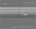
상기 실시예들 및 비교예에서 제조된 포토레지스트 조성물을 사용하여 포토레지스트 막들을 형성하였다. 이어서, 상기 포토레지스트 막들에 대하여 현상 공정을 수행한 후 상기 포토레지스트막의 손상 정도를 평가하였다. 이에 따른 결과를 하기 표 2, 도 12 및 도 13에 나타낸다. 구체적으로, 상기 실시예 1 내지 3 및 비교예에서 제조된 포토레지스트 조성물을 베어 웨이퍼(bare wafer)상에 도포하여 포토레지스트 막들을 형성하였다. 이어서, 상기 포토레지스트 막을 소프트 베이킹 하였다. 이 경우, 상기 비교예에서 제조된 포토레지스트 조성물을 사용하여 총 3개의 포토레지스트 막을 형성하였다. 이 중, 제1 포토레지스트막은 122℃에서 200초 동안 소프트 베이킹 하였으며, 베이킹 후의 두께는 13.47㎛이었다. 또한, 비교예에 따라 형성된 포토레지스트 막 중 제2 포토레지스트막 및 제3 포토레지스트막은 119℃의 온도에서 240초 동안 소프트 베이킹 하였으며, 베이킹 후의 두께는 각각13.42㎛ 및 12.00㎛ 이었다. 상기 실시예 1 내지 실시예 3에서 제조된 포토레지스트 조성물들을 사용하여 형성된 포토레지스트막들은 119℃의 온도에서 240초 동안 소프트 베이킹 하였다. 상기 소프트 베이킹 공정 수행 후 상기 실시예 1 내지 3에서 제조된 포토레지스트 조성물을 사용하여 형성된 포토레지스트 막들의 두께는 모두 12.0㎛이었다. 이어서, 상기 포토레지스트막을 TMAH(2.38 중량%의 수용액)를 사용하여 현상하였다.Photoresist films were formed using the photoresist compositions prepared in the above Examples and Comparative Examples. Subsequently, after the development process was performed on the photoresist films, the degree of damage of the photoresist films was evaluated. The results are shown in Table 2, FIG. 12 and FIG. 13. Specifically, the photoresist compositions prepared in Examples 1 to 3 and Comparative Examples were applied onto a bare wafer to form photoresist films. Subsequently, the photoresist film was soft baked. In this case, a total of three photoresist films were formed using the photoresist composition prepared in Comparative Example. Among them, the first photoresist film was soft baked at 122 ° C. for 200 seconds, and the thickness after baking was 13.47 μm. Further, the second photoresist film and the third photoresist film of the photoresist film formed according to the comparative example were soft baked at a temperature of 119 ° C. for 240 seconds, and the thicknesses after baking were 13.42 μm and 12.00 μm, respectively. The photoresist films formed using the photoresist compositions prepared in Examples 1 to 3 were soft baked at a temperature of 119 ° C. for 240 seconds. After performing the soft baking process, the thicknesses of the photoresist films formed using the photoresist compositions prepared in Examples 1 to 3 were all 12.0 μm. The photoresist film was then developed using TMAH (2.38 wt% aqueous solution).
도 12 및 도 13은 상기 실시예 및 비교예에 따라 제조된 포토레지스트막을 현상한 결과를 나타내는 전자현미경 사진들이다. 구체적으로, 도 12는 상기 실시예 1에 따른 포토레지스트막을 현상한 결과를 나타내는 전자현미경 사진이며, 도 13은 상기 비교예에 따른 제3 포토레지스트막을 현상한 결과를 나타내는 전자현미경 사진이다.12 and 13 are electron micrographs showing the results of developing the photoresist films prepared according to the above Examples and Comparative Examples. Specifically, FIG. 12 is an electron micrograph showing a result of developing the photoresist film according to Example 1, and FIG. 13 is an electron micrograph showing a result of developing the third photoresist film according to the comparative example.
표 2, 도 12 및 도 13을 참조하면, 수소 결합 화합물을 포함하지 않은 포토레지스트 막들에 비하여, 수소 결합 화합물을 포함하는 포토레지스트막의 손상 정도가 현저히 감소된 것을 확인할 수 있다. 구체적으로 비교예에 따른 제1 포토레지스트막의 손실율은 21.75%, 제2 포토레지스트막의 손실율은 21.98%, 제3 포토레지스트막의 손실율은 24.17%로써, 모두 20% 이상의 손실율을 나타낸다. 반면, 실시예 1의 포토레지스트막의 손실율은 15.83%, 실시예 2의 포토레지스트막의 손실율은 12.5%, 실시예 3의 포토레지스트막의 손실율은 11.67%로써 모두 20%를 현저히 밑도는 손실율을 나타내고 있다. 이에 따라, 본 발명에 따른 포토레지스트 조성물에 포함된 수소 결합 화합물이 열경화성 수지 분자 사이의 인력을 증가시킴으로써 현상 공정에서 발생할 수 있는 포토레지스트막의 손상을 최소화할 수 있음을 알 수 있다.Referring to Table 2, FIG. 12 and FIG. 13, it can be seen that the damage of the photoresist film including the hydrogen bonding compound is significantly reduced compared to the photoresist films not including the hydrogen bonding compound. Specifically, the loss rate of the first photoresist film is 21.75%, the loss rate of the second photoresist film is 21.98%, and the loss rate of the third photoresist film is 24.17%, all showing a loss rate of 20% or more. On the other hand, the loss rate of the photoresist film of Example 1 was 15.83%, the loss rate of the photoresist film of Example 2 was 12.5%, and the loss rate of the photoresist film of Example 3 was 11.67%, which is significantly lower than 20%. Accordingly, it can be seen that the hydrogen bonding compound included in the photoresist composition according to the present invention can minimize the damage of the photoresist film that may occur in the developing process by increasing the attractive force between the thermosetting resin molecules.
또한, 실시예 1 내지 3에 있어서, 수소 결합 화합물의 함량이 증가할수록 포토레지스트막의 손상 정도가 줄어드는 것을 확인할 수 있다. 그러나 수소 결합 화합물의 함량이 지나치게 증가하는 경우, 후속의 현상 과정에서 패턴을 정확하게 형성하기가 어려워지므로 약 2중량% 이하의 수소 결합 화합물을 포함하는 것이 바람직하다. 한편, 실시예 4 및 5에서 제조된 포토레지스트 조성물을 이용하여 포토레지스트막을 형성한 경우에도, 실시예 1 내지 3의 경우와 마찬가지로 현상 과정에서 포토레지스트막의 손상이 방지되는 것으로 나타났다.In addition, in Examples 1 to 3, it can be seen that the damage degree of the photoresist film decreases as the content of the hydrogen bonding compound increases. However, when the content of the hydrogen bond compound is excessively increased, it is preferable to include about 2 wt% or less of the hydrogen bond compound because it becomes difficult to accurately form a pattern in the subsequent development process. On the other hand, even when the photoresist film was formed using the photoresist compositions prepared in Examples 4 and 5, it was shown that damage to the photoresist film was prevented during the development process as in the case of Examples 1 to 3.
본 발명의 포토레지스트 조성물을 사용하여 반도체 장치의 보호막을 형성한다. 이에 따라, 상기 포토레지스트 조성물에 포함된 수소 결합 화합물이 열경화성 수지에 포함된 수소와 결합하여 열경화성 수지 분자간의 상호 결합력이 증가된다. 이에 따라, 현상과정에서 발생할 수 있는 보호막의 손실을 최소화할 수 있으며, 상 대적으로 낮은 비용으로 완성된 반도체 소자를 효과적으로 패시베이션할 수 있는 보호막을 형성할 수 있다. 결과적으로, 반도체 장치의 불량을 방지함과 동시에 반도체 제조 공정의 생산성을 향상시킬 수 있게 된다.The protective film of a semiconductor device is formed using the photoresist composition of this invention. Accordingly, the hydrogen bonding compound included in the photoresist composition is combined with the hydrogen contained in the thermosetting resin to increase the mutual bonding force between the thermosetting resin molecules. Accordingly, it is possible to minimize the loss of the protective film that can occur during the development process, it is possible to form a protective film that can effectively passivate the completed semiconductor device at a relatively low cost. As a result, the defect of a semiconductor device can be prevented and the productivity of a semiconductor manufacturing process can be improved.
이상, 본 발명의 바람직한 실시예를 참조하여 설명하였지만 해당 기술 분야의 숙련된 당업자라면 하기의 특허 청구의 범위에 기재된 본 발명의 사상 및 영역으로부터 벗어나지 않는 범위 내에서 본 발명을 다양하게 수정 및 변경시킬 수 있음을 이해할 수 있을 것이다.Although the above has been described with reference to the preferred embodiments of the present invention, those skilled in the art will be able to variously modify and change the present invention without departing from the spirit and scope of the present invention as set forth in the claims below. It will be appreciated.
Claims (44)
Translated fromKorean


Applications Claiming Priority (2)
| Application Number | Priority Date | Filing Date | Title |
|---|---|---|---|
| KR20050003161 | 2005-01-13 | ||
| KR1020050003161 | 2005-01-13 |
Publications (2)
| Publication Number | Publication Date |
|---|---|
| KR20060082787A KR20060082787A (en) | 2006-07-19 |
| KR100729256B1true KR100729256B1 (en) | 2007-06-15 |
Family
ID=36653648
Family Applications (1)
| Application Number | Title | Priority Date | Filing Date |
|---|---|---|---|
| KR1020050130524AExpired - Fee RelatedKR100729256B1 (en) | 2005-01-13 | 2005-12-27 | Photoresist composition, method for forming a photoresist pattern and method for forming a protection layer of a semiconductor device using the photoresist composition |
Country Status (2)
| Country | Link |
|---|---|
| US (1) | US20060154176A1 (en) |
| KR (1) | KR100729256B1 (en) |
Families Citing this family (7)
| Publication number | Priority date | Publication date | Assignee | Title |
|---|---|---|---|---|
| US7620895B2 (en)* | 2004-09-08 | 2009-11-17 | Transcensus, Llc | Systems and methods for teaching a person to interact with a computer program having a graphical user interface |
| US8187788B2 (en)* | 2006-04-28 | 2012-05-29 | Asahi Kasei Kabushiki Kaisha | Photosensitive resin composition and photosensitive film |
| KR101141987B1 (en)* | 2008-08-20 | 2012-05-17 | 엔엘티 테크놀로지 가부시키가이샤 | Chemical liquid for dissolution modification and dissolution modification processesing method |
| KR20110118899A (en)* | 2010-04-26 | 2011-11-02 | 삼성전자주식회사 | Composition for forming protective film and method of forming protective film using same |
| KR102126894B1 (en)* | 2013-03-11 | 2020-06-25 | 주식회사 동진쎄미켐 | Resist protective film composition for lithography process and method for forming pattern of semiconductor device |
| EP3585825A1 (en)* | 2017-02-24 | 2020-01-01 | SI Group, Inc. | Resins having a high methylol to dibenzyl ether ratio and methods of making the same |
| JP2018151527A (en)* | 2017-03-13 | 2018-09-27 | 日立化成デュポンマイクロシステムズ株式会社 | Photosensitive resin composition |
Citations (3)
| Publication number | Priority date | Publication date | Assignee | Title |
|---|---|---|---|---|
| KR20010062829A (en)* | 1999-12-28 | 2001-07-07 | 후루타 다케시 | Epoxy-modified polyimide, photosensitive composition, coverlay film, solder resist, and printed wiring board using the epoxy-modified polyimide |
| KR20040004383A (en)* | 2000-09-29 | 2004-01-13 | 니폰 제온 가부시키가이샤 | Photoresist composition for forming insulation film, insulation film for organic electroluminescence element and method for its formation |
| KR20040012763A (en)* | 2001-04-19 | 2004-02-11 | 제너럴 일렉트릭 캄파니 | Methods for embossing and embossed articles formed thereby |
Family Cites Families (16)
| Publication number | Priority date | Publication date | Assignee | Title |
|---|---|---|---|---|
| JPS56150830A (en)* | 1980-04-25 | 1981-11-21 | Hitachi Ltd | Semiconductor device |
| US4827326A (en)* | 1987-11-02 | 1989-05-02 | Motorola, Inc. | Integrated circuit having polyimide/metal passivation layer and method of manufacture using metal lift-off |
| CA2040994A1 (en)* | 1990-05-08 | 1991-11-09 | David D. Ngo | Photoimageable polyimide coating |
| US5194928A (en)* | 1991-01-14 | 1993-03-16 | International Business Machines Corporation | Passivation of metal in metal/polyimide structure |
| US5177181A (en)* | 1991-06-06 | 1993-01-05 | Occidental Chemical Corporation | Diamines and photosensitive polyimides made therefrom |
| KR0134753B1 (en)* | 1993-02-26 | 1998-04-18 | 사토 후미오 | Polyamic acid composition |
| DE59808434D1 (en)* | 1997-11-28 | 2003-06-26 | Infineon Technologies Ag | Chemically amplified resist for electron beam lithography |
| US6338936B1 (en)* | 1998-02-02 | 2002-01-15 | Taiyo Ink Manufacturing Co., Ltd. | Photosensitive resin composition and method for formation of resist pattern by use thereof |
| TW495646B (en)* | 1999-12-27 | 2002-07-21 | Fuji Photo Film Co Ltd | Positive-working radiation-sensitive composition |
| DE60103529T2 (en)* | 2000-03-29 | 2005-06-02 | Kanagawa University, Yokohama | CURING COMPOSITION THAT IS CURED BY LIGHT AND HEAT, A LIGHT-SENSITIVE DRYER MANUFACTURED FROM THIS PRODUCT, AND METHOD FOR FORMING A PATTERN THEREFOR |
| US6703433B1 (en)* | 2000-05-12 | 2004-03-09 | Dow Corning Corporation | Radiation curable compositions containing alkenyl ether functional polyisobutylenes |
| SG118142A1 (en)* | 2001-07-06 | 2006-01-27 | Toray Industries | Resin composition adhesive film for semiconductor device and laminated film with metallic foil and semiconductor device using the same |
| KR100529577B1 (en)* | 2001-11-22 | 2005-11-17 | 미쓰이 가가쿠 가부시키가이샤 | Photosensitive resin compositions, dry film, and a product using the same |
| US6660624B2 (en)* | 2002-02-14 | 2003-12-09 | Taiwan Semiconductor Manufacturing Co., Ltd. | Method for reducing fluorine induced defects on a bonding pad surface |
| KR100532590B1 (en)* | 2002-11-07 | 2005-12-01 | 삼성전자주식회사 | Soluble Polyimide for photosensitive polyimide and photosensitive polyimide composition comprising the soluble polyimide |
| KR100576357B1 (en)* | 2003-10-21 | 2006-05-03 | 삼성전자주식회사 | Resol-containing resin solution, a thermosetting resin film formed using the same, and a method of forming a thermosetting resin film using the same |
- 2005
- 2005-12-27KRKR1020050130524Apatent/KR100729256B1/ennot_activeExpired - Fee Related
- 2006
- 2006-01-11USUS11/331,305patent/US20060154176A1/ennot_activeAbandoned
Patent Citations (3)
| Publication number | Priority date | Publication date | Assignee | Title |
|---|---|---|---|---|
| KR20010062829A (en)* | 1999-12-28 | 2001-07-07 | 후루타 다케시 | Epoxy-modified polyimide, photosensitive composition, coverlay film, solder resist, and printed wiring board using the epoxy-modified polyimide |
| KR20040004383A (en)* | 2000-09-29 | 2004-01-13 | 니폰 제온 가부시키가이샤 | Photoresist composition for forming insulation film, insulation film for organic electroluminescence element and method for its formation |
| KR20040012763A (en)* | 2001-04-19 | 2004-02-11 | 제너럴 일렉트릭 캄파니 | Methods for embossing and embossed articles formed thereby |
Also Published As
| Publication number | Publication date |
|---|---|
| KR20060082787A (en) | 2006-07-19 |
| US20060154176A1 (en) | 2006-07-13 |
Similar Documents
| Publication | Publication Date | Title |
|---|---|---|
| KR102380068B1 (en) | Resin composition, cured film, semiconductor device, and manufacturing method thereof | |
| TWI658063B (en) | Photosensitive resin composition, production method of patterned hardened film using the same, patterned hardened film and semiconductor device | |
| JP3958011B2 (en) | Positive photosensitive resin composition, method for producing positive photosensitive resin composition, and semiconductor device | |
| US12210285B2 (en) | Resin composition, resin sheet, cured film, method for producing cured film, semiconductor device, and display device | |
| US6436593B1 (en) | Positive photosensitive resin composition, process for producing pattern and electronic parts | |
| KR20110118899A (en) | Composition for forming protective film and method of forming protective film using same | |
| JP6888660B2 (en) | Resin composition containing polyimide precursor, method for manufacturing cured film and electronic components | |
| JP6390165B2 (en) | Polyimide precursor, photosensitive resin composition containing the polyimide precursor, pattern cured film manufacturing method using the same, and semiconductor device | |
| JP2008133423A (en) | Adhesive composition for semiconductor, semiconductor device using the same and method for producing the semiconductor device | |
| JPWO2018043250A1 (en) | Photosensitive resin composition, cured film, organic EL display device, semiconductor electronic component, semiconductor device | |
| WO2013122208A1 (en) | Photosensitive resin composition, method for producing patterned cured film, and electronic component | |
| US20060154176A1 (en) | Photoresist composition, method of forming a photoresist pattern and method of forming a protection layer in a semiconductor device using the photoresist composition | |
| WO2017217293A1 (en) | Photosensitive resin composition | |
| US20080187867A1 (en) | Photosensitive polyimide composition, polyimide film and semiconductor device using the same | |
| JP2014201696A (en) | Polyimide precursor, photosensitive resin composition comprising the polyimide precursor, and method of producing patterned cured film using the same | |
| JP2003084435A (en) | Negative photosensitive resin composition, method for producing pattern and electronic parts | |
| JP2015113429A (en) | Polyimide precursor resin composition | |
| JPWO2005027601A1 (en) | Insulating pattern and method for forming the same | |
| KR20180048679A (en) | Resin composition | |
| TWI417941B (en) | Method of preparing a patterned film with a developing solvent | |
| US7528188B2 (en) | Resin solution and method of forming a protection layer | |
| TW202104371A (en) | Photosensitive polyimide resin composition | |
| JP2011046918A (en) | Resin composition for insulating film or surface-protective film of electronic components, method for producing pattern-cured film and electronic component | |
| JP2004062142A (en) | Positive photosensitive resin composition, method for manufacturing pattern, and electronic parts | |
| JP3651529B2 (en) | Photosensitive resin composition |
Legal Events
| Date | Code | Title | Description |
|---|---|---|---|
| A201 | Request for examination | ||
| PA0109 | Patent application | St.27 status event code:A-0-1-A10-A12-nap-PA0109 | |
| PA0201 | Request for examination | St.27 status event code:A-1-2-D10-D11-exm-PA0201 | |
| PG1501 | Laying open of application | St.27 status event code:A-1-1-Q10-Q12-nap-PG1501 | |
| D13-X000 | Search requested | St.27 status event code:A-1-2-D10-D13-srh-X000 | |
| D14-X000 | Search report completed | St.27 status event code:A-1-2-D10-D14-srh-X000 | |
| E902 | Notification of reason for refusal | ||
| PE0902 | Notice of grounds for rejection | St.27 status event code:A-1-2-D10-D21-exm-PE0902 | |
| E13-X000 | Pre-grant limitation requested | St.27 status event code:A-2-3-E10-E13-lim-X000 | |
| P11-X000 | Amendment of application requested | St.27 status event code:A-2-2-P10-P11-nap-X000 | |
| P13-X000 | Application amended | St.27 status event code:A-2-2-P10-P13-nap-X000 | |
| E701 | Decision to grant or registration of patent right | ||
| PE0701 | Decision of registration | St.27 status event code:A-1-2-D10-D22-exm-PE0701 | |
| GRNT | Written decision to grant | ||
| PR0701 | Registration of establishment | St.27 status event code:A-2-4-F10-F11-exm-PR0701 | |
| PR1002 | Payment of registration fee | St.27 status event code:A-2-2-U10-U11-oth-PR1002 Fee payment year number:1 | |
| PG1601 | Publication of registration | St.27 status event code:A-4-4-Q10-Q13-nap-PG1601 | |
| G170 | Re-publication after modification of scope of protection [patent] | ||
| PG1701 | Publication of correction | St.27 status event code:A-5-5-P10-P19-oth-PG1701 Patent document republication publication date:20080423 Republication note text:Request for Correction Notice (Document Request) Gazette number:1007292560000 Gazette reference publication date:20070615 | |
| PR1001 | Payment of annual fee | St.27 status event code:A-4-4-U10-U11-oth-PR1001 Fee payment year number:4 | |
| PR1001 | Payment of annual fee | St.27 status event code:A-4-4-U10-U11-oth-PR1001 Fee payment year number:5 | |
| PR1001 | Payment of annual fee | St.27 status event code:A-4-4-U10-U11-oth-PR1001 Fee payment year number:6 | |
| R18-X000 | Changes to party contact information recorded | St.27 status event code:A-5-5-R10-R18-oth-X000 | |
| FPAY | Annual fee payment | Payment date:20130531 Year of fee payment:7 | |
| PR1001 | Payment of annual fee | St.27 status event code:A-4-4-U10-U11-oth-PR1001 Fee payment year number:7 | |
| FPAY | Annual fee payment | Payment date:20140530 Year of fee payment:8 | |
| PR1001 | Payment of annual fee | St.27 status event code:A-4-4-U10-U11-oth-PR1001 Fee payment year number:8 | |
| FPAY | Annual fee payment | Payment date:20150601 Year of fee payment:9 | |
| PR1001 | Payment of annual fee | St.27 status event code:A-4-4-U10-U11-oth-PR1001 Fee payment year number:9 | |
| LAPS | Lapse due to unpaid annual fee | ||
| PC1903 | Unpaid annual fee | St.27 status event code:A-4-4-U10-U13-oth-PC1903 Not in force date:20160612 Payment event data comment text:Termination Category : DEFAULT_OF_REGISTRATION_FEE | |
| PC1903 | Unpaid annual fee | St.27 status event code:N-4-6-H10-H13-oth-PC1903 Ip right cessation event data comment text:Termination Category : DEFAULT_OF_REGISTRATION_FEE Not in force date:20160612 |