KR100728570B1 - Current control device of semiconductor memory - Google Patents
Current control device of semiconductor memoryDownload PDFInfo
- Publication number
- KR100728570B1 KR100728570B1KR1020050133713AKR20050133713AKR100728570B1KR 100728570 B1KR100728570 B1KR 100728570B1KR 1020050133713 AKR1020050133713 AKR 1020050133713AKR 20050133713 AKR20050133713 AKR 20050133713AKR 100728570 B1KR100728570 B1KR 100728570B1
- Authority
- KR
- South Korea
- Prior art keywords
- code
- bias voltage
- transistor
- current
- inverter
- Prior art date
- Legal status (The legal status is an assumption and is not a legal conclusion. Google has not performed a legal analysis and makes no representation as to the accuracy of the status listed.)
- Expired - Fee Related
Links
Images


Classifications
- G—PHYSICS
- G11—INFORMATION STORAGE
- G11C—STATIC STORES
- G11C5/00—Details of stores covered by group G11C11/00
- G11C5/14—Power supply arrangements, e.g. power down, chip selection or deselection, layout of wirings or power grids, or multiple supply levels
- G11C5/147—Voltage reference generators, voltage or current regulators; Internally lowered supply levels; Compensation for voltage drops
- G—PHYSICS
- G11—INFORMATION STORAGE
- G11C—STATIC STORES
- G11C7/00—Arrangements for writing information into, or reading information out from, a digital store
- G11C7/06—Sense amplifiers; Associated circuits, e.g. timing or triggering circuits
- G—PHYSICS
- G11—INFORMATION STORAGE
- G11C—STATIC STORES
- G11C7/00—Arrangements for writing information into, or reading information out from, a digital store
- G11C7/12—Bit line control circuits, e.g. drivers, boosters, pull-up circuits, pull-down circuits, precharging circuits, equalising circuits, for bit lines
Landscapes
- Engineering & Computer Science (AREA)
- Power Engineering (AREA)
- Static Random-Access Memory (AREA)
Abstract
Translated fromKoreanDescription
Translated fromKorean도 1은 종래의 기술에 따른 반도체 메모리의 구조를 나타낸 회로도,1 is a circuit diagram showing the structure of a semiconductor memory according to the prior art;
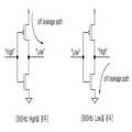
도 2는 도 1의 BIS 리피터(Bit line Isolation Signal Repeater)의 누설전류 패스를 보여주기 위한 회로도,FIG. 2 is a circuit diagram illustrating a leakage current path of a bit line isolation signal repeater of FIG. 1;
도 3은 도 1의 BIS 리피터의 누설전류 특성을 나타낸 그래프,3 is a graph showing the leakage current characteristics of the BIS repeater of FIG.
도 4는 본 발명에 따른 반도체 메모리의 전류 제어장치의 구성을 나타낸 블록도,4 is a block diagram showing the configuration of a current control device of a semiconductor memory according to the present invention;
도 5는 도 4의 전류 제어부의 내부 구성을 나타낸 회로도,5 is a circuit diagram illustrating an internal configuration of the current controller of FIG. 4;
도 6은 본 발명에 따른 BIS 리피터의 누설전류 특성을 나타낸 그래프이다.6 is a graph showing the leakage current characteristics of the BIS repeater according to the present invention.
< 도면의 주요 부분에 대한 부호의 설명 ><Description of Symbols for Main Parts of Drawings>
400: 전류 제어부 410: 전류 차단부400: current control unit 410: current interrupting unit
420: 바이어스 전압 생성부 421: 코드 설정부420: bias voltage generator 421: code setting unit
422: 디코더 423: 전압 출력부422: decoder 423: voltage output unit
본 발명은 반도체 메모리에 관한 것으로서, 특히 반도체 메모리의 전류 제어장치에 관한 것이다.BACKGROUND OF THE
종래의 기술에 따른 반도체 메모리는 도 1에 도시된 바와 같이, 메모리 셀 어레이가 복수개의 메모리셀 블록(Block0, Block1, …)으로 나누어지고, 1쌍의 이웃하는 메모리셀 블록(Block0, Block1)의 비트라인쌍(BL1, BL1b)(BL2, BL2b)이 하나의 센스앰프(Sense Amplifier, SA)를 공유하도록 구성된다.In the semiconductor memory according to the related art, as shown in FIG. 1, a memory cell array is divided into a plurality of memory cell blocks Block0, Block1,..., And a pair of neighboring memory cell blocks Block0, Block1, respectively. The bit line pairs BL1 and BL1b BL2 and BL2b are configured to share one sense amplifier SA.
그리고 상기 비트라인쌍(BL1, BL1b)(BL2, BL2b)을 연결하기 위한 스위칭 수단(SASH1, SASH2)(SASL1, SASL2)이 구비된다.Switching means SASH1 and SASH2 SASL1 and SASL2 for connecting the bit line pairs BL1 and BL1b BL2 and BL2b are provided.
상기 스위칭 수단(SASH1, SASH2)(SASL1, SASL2)은 각각 비트라인 아이솔레이션 신호(BISH, BISL)에 의해 구동된다.The switching means SASH1 and SASH2 SASL1 and SASL2 are driven by bit line isolation signals BISH and BISL, respectively.
예를 들어, 상측 메모리셀 블록(Block0)으로부터 데이터를 센싱하기 위해서는 상기 스위칭 수단(SASH1, SASH2)에 상기 비트라인 아이솔레이션 신호(BISH)를 인가하여 해당 비트라인 쌍(BL1, BL1b)을 센스앰프에 연결시킨다.For example, in order to sense data from the upper memory cell block Block0, the bit line isolation signal BISH is applied to the switching means SASH1 and SASH2 so that the corresponding bit line pairs BL1 and BL1b are applied to a sense amplifier. Connect it.
상기 비트라인 아이솔레이션 신호(BISH, BISL)를 전송하기 위한 신호라인의 길이에 따라 신호감쇄가 발생할 수 있으므로 각 신호라인마다 BIS 리피터(Bit line Isolation Signal Repeater)(11)가 연결되며, 상기 BIS 리피터(11)는 인버터로 구성된다.Since signal attenuation may occur depending on the length of the signal line for transmitting the bit line isolation signals BISH and BISL, a
이때 비트라인 아이솔레이션 신호 생성회로는 반전된 비트라인 아이솔레이션 신호(BISHb, BISLb)를 출력하고, 상기 BIS 리피터(11)가 상기 반전된 비트라인 아이솔레이션 신호(BISHb, BISLb)를 반전시킨 비트라인 아이솔레이션 신호(BISH, BISL)를 해당 스위칭 수단(SASH, SASL)에 공급한다.At this time, the bit line isolation signal generation circuit outputs the inverted bit line isolation signals BISHb and BISLb, and the
상기 BIS 리피터(11) 즉, 인버터는 셀 밀도가 증가할수록 즉, 메모리 용량이 증가함에 따라 채널 랭쓰(Channel Length)가 감소하면서 숏 채널 이펙트(Short Channel Effect)로 인하여 누설전류가 증가하고 있다.As the cell density increases, that is, as the memory capacity increases, the
즉, 도 2에 도시된 바와 같이, 비트라인 아이솔레이션 신호(BISHb)가 하이(High)일 경우 인버터의 NMOS 트랜지스터가 온 되고, PMOS 트랜지스터는 오프된다.That is, as shown in FIG. 2, when the bit line isolation signal BISHb is high, the NMOS transistor of the inverter is turned on and the PMOS transistor is turned off.
이때 오프된 PMOS 트랜지스터를 통해 누설전류 패스가 형성된다.At this time, a leakage current path is formed through the turned off PMOS transistor.
그 반대의 경우, 비트라인 아이솔레이션 신호(BISHb)가 로우(Low)일 경우 인버터의 NMOS 트랜지스터가 오프 되고, PMOS 트랜지스터는 온 된다.In the opposite case, when the bit line isolation signal BISHb is low, the NMOS transistor of the inverter is turned off and the PMOS transistor is turned on.
이때 오프된 NMOS 트랜지스터를 통해 누설전류 패스가 형성된다.At this time, a leakage current path is formed through the turned off NMOS transistor.
상기 PMOS 트랜지스터 및 NMOS 트랜지스터의 누설전류 패스에 따른 누설전류 특성이 도 3에 도시되어 있다. 도 3에 도시된 바와 같이, PMOS 트랜지스터 및 NMOS 트랜지스터 모두 오프 상태에서 인가된 전원전압(VDD)에 비례하여 누설전류가 증가하고 있으며, 특히 PMOS 트랜지스터의 누설전류가 NMOS 트랜지스터에 비해 큰 것을 알 수 있다.The leakage current characteristic of the PMOS transistor and the NMOS transistor according to the leakage current path is shown in FIG. 3. As shown in FIG. 3, both the PMOS transistor and the NMOS transistor are increased in proportion to the power supply voltage VDD applied in the off state, and the leakage current of the PMOS transistor is larger than that of the NMOS transistor. .
또한 트랜지스터의 드레인에 인가된 전원전압(VDD)이 동작전압에 비해 높다는 것이 누설전류를 더욱 증가시키는 요인으로 작용한다.In addition, the fact that the power supply voltage VDD applied to the drain of the transistor is higher than the operating voltage acts as an additional factor to increase the leakage current.
이와 같이 종래의 기술에 따른 반도체 메모리는 BIS 리피터로 사용되는 인버터의 누설전류량이 상당히 크고, 메모리 용량이 커짐에 따라 BIS 리피터로 사용되는 인버터의 수가 더욱 증가하므로 메모리 전체에서 발생되는 누설전류가 소비전류 규격을 초과할 정도로 커지는 문제점이 있다.As described above, in the semiconductor memory according to the related art, the leakage current of an inverter used as a BIS repeater is considerably large, and as the memory capacity increases, the number of inverters used as a BIS repeater increases further, so that the leakage current generated in the entire memory consumes current. There is a problem that becomes large enough to exceed the specification.
본 발명은 상술한 종래의 문제점을 해결하기 위하여 안출한 것으로서, 인버터의 누설전류를 최소화할 수 있도록 한 반도체 메모리의 전류 제어장치를 제공함에 그 목적이 있다.SUMMARY OF THE INVENTION The present invention has been made in view of the above-mentioned problems, and an object thereof is to provide a current control apparatus of a semiconductor memory capable of minimizing leakage current of an inverter.
본 발명에 따른 반도체 메모리의 전류 제어장치는 인버터, 및 전원단과 상기 인버터 사이에 연결되어 대기신호에 따라 상기 인버터로 공급되는 전류를 제어하는 전류 제어부를 포함하는 것을 특징으로 한다.The current control apparatus of the semiconductor memory according to the present invention is characterized in that it comprises an inverter and a current control unit connected between a power supply terminal and the inverter to control the current supplied to the inverter according to the standby signal.
이하, 첨부된 도면을 참조하여 본 발명에 따른 반도체 메모리의 전류 제어장치의 바람직한 실시예를 설명하면 다음과 같다.Hereinafter, with reference to the accompanying drawings will be described a preferred embodiment of the current control apparatus of the semiconductor memory according to the present invention.
도 4는 본 발명에 따른 반도체 메모리의 전류 제어장치의 구성을 나타낸 블록도, 도 5는 도 4의 전류 제어부의 내부 구성을 나타낸 회로도, 도 6은 본 발명에 따른 BIS 리피터의 누설전류 특성을 나타낸 그래프이다.Figure 4 is a block diagram showing the configuration of the current control device of the semiconductor memory according to the present invention, Figure 5 is a circuit diagram showing the internal configuration of the current control unit of Figure 4, Figure 6 shows the leakage current characteristics of the BIS repeater according to the present invention It is a graph.
본 발명에 따른 반도체 메모리의 전류 제어장치는 도 4에 도시된 바와 같이, 복수개의 메모리 셀 블록(Block0, Block1, …), 이웃하는 두개의 메모리 셀 블록(Block0, Block1)과 연결된 제 1 및 제 2 비트라인쌍(BL1, BL1b)(BL2, BL2b), 상기 제 1 및 제 2 비트라인쌍(BL1, BL1b)(BL2, BL2b)과 센스앰프(SA)를 연결시키기 위한 제 1 및 제 2 스위칭 소자쌍(SASH1, SASH2)(SASL1, SASL2), 상기 제 1 및 제 2 스위칭 소자쌍(SASH1, SASH2)(SASL1, SASL2)을 각각 구동하기 위한 비트라인 아이 솔레이션 신호라인(BISH, BISL), 각 비트라인 아이솔레이션 신호라인(BISH, BISL)에 연결된 BIS 리피터(Bit line Isolation Signal Repeater)(11), 일단이 전원단과 연결되고 타단이 상기 각 BIS 리피터(11)에 공통 연결되어 대기신호에 따라 상기 BIS 리피터(11)로 공급되는 전류를 제어하는 전류 제어부(400)를 포함한다.As shown in FIG. 4, the current control apparatus of the semiconductor memory according to the present invention includes a plurality of memory cell blocks Block0, Block1, ..., and first and second devices connected to two neighboring memory cell blocks Block0, Block1. First and second switching for connecting the two bit line pairs BL1 and BL1b BL2 and BL2b, the first and second bit line pairs BL1 and BL1b BL2 and BL2b, and the sense amplifier SA. Bit line isolation signal lines BISH and BISL for driving the device pairs SASH1 and SASH2 (SASL1 and SASL2) and the first and second switching element pairs SASH1 and SASH2 (SASL1 and SASL2), respectively. A bit line isolation signal repeater (11) connected to each bit line isolation signal line (BISH, BISL), one end of which is connected to the power supply terminal and the other end of which is commonly connected to the
상기 전류 제어부(400)는 도 5에 도시된 바와 같이, 대기신호(std)에 따라 기설정된 바이어스 전압(V_var)을 이용하여 상기 BIS 리피터(11)로 공급되는 전원전류를 차단하는 전류 차단부(410), 및 소정 코드에 해당하는 레벨을 갖는 상기 바이어스 전압(V_var)을 생성하는 바이어스 전압 생성부(420)를 포함한다.As shown in FIG. 5, the
이때 대기신호(std)는 대기모드의 경우 인에이블(예를 들어, 하이) 되고, 대기모드가 아닐 경우 디스에이블(예를 들어, 로우) 되는 신호이다.At this time, the standby signal std is a signal that is enabled (for example, high) in the standby mode and is disabled (for example, low) in the standby mode.
상기 전류 차단부(410)는 상기 대기신호(std)를 입력받는 인버터(IV11), 상기 전원단(VDD)에 드레인이 연결되고, 상기 BIS 리피터(11)에 소오스가 연결되며, 상기 인버터(IV11)의 출력을 게이트에 입력받는 제 1 트랜지스터(M11), 상기 바이어스 전압(V_var)을 드레인에 입력받고, 상기 제 1 트랜지스터(M11)와 상기 BIS 리피터(11)의 연결노드에 소오스가 연결되며, 상기 대기신호(std)를 게이트에 입력받는 제 2 트랜지스터(M12)를 포함한다.The
상기 바이어스 전압 생성부(420)는 바이어스 전압(V_var)의 레벨을 정하기 위한 코드(TMC0 ~ TMC2)를 설정하는 코드 설정부(421), 상기 코드 설정부(421)에서 설정된 코드(TMC0 ~ TMC2)를 디코딩한 디코딩값을 출력하는 디코더(422), 상기 디코딩값에 해당하는 레벨의 바이어스 전압(V_var)을 출력하는 전압 출력부(423)를 포함한다.The
상기 코드 설정부(421)는 코드(TMC0 ~ TMC2)의 비트수에 해당하는 3개의 코드 설정유닛(421-1, 421-2, 421-3)으로 구성된다. 그 중 하나의 코드 설정유닛(421-1)의 구성을 설명하면, 접지단에 연결된 퓨즈(F21),소오스가 전원단(VDD)에 연결되고, 드레인이 상기 퓨즈(F21)와 연결되며, 게이트에 해당 코드의 비트값(TMC0)을 입력받는 제 3 트랜지스터(M21), 드레인이 상기 퓨즈(F21)와 연결되고 게이트에 리셋신호(RESET)를 입력받는 제 4 트랜지스터(M22), 드레인이 상기 제 4 트랜지스터(M22)의 소오스와 연결되고 소오스가 접지되며 게이트에 전원단(VDD)이 연결된 제 5 트랜지스터(M23), 및 상기 퓨즈(F21)와 상기 제 4 트랜지스터(M22)의 연결노드에 연결된 버터(B21)를 포함한다. 상기 코드 설정유닛(421-2, 421-3)은 각각 해당 코드의 비트값(TMC1, TMC2)이 입력되는 것이 다를 뿐, 내부 구성은 동일하므로 구성설명은 생략하기로 한다.The
상기 전압 출력부(423)는 전원단(VDD)과 접지단 사이에 연결된 복수개의 저항소자, 각각의 소오스가 상기 복수개의 저항소자 사이의 연결노드에 연결되고 드레인이 공통 연결되며 게이트에 입력된 디코딩값에 따라 온 되어 상기 저항소자에 의해 분배된 전원전압을 바이어스 전압(V_var)으로 출력하는 복수개의 트랜지스터를 포함한다.The
이와 같이 구성된 본 발명에 따른 반도체 메모리의 전류 제어장치의 동작을 도 4 내지 도 6을 참조하여 설명하면 다음과 같다.The operation of the current control device of the semiconductor memory according to the present invention configured as described above will be described with reference to FIGS. 4 to 6.
먼저, 반도체 메모리가 노멀 동작할 경우의 전류 제어부(400)의 동작을 설명 하면 다음과 같다.First, the operation of the
이때 대기신호(std)가 로우이므로 도 5의 전류 차단부(410)의 인버터(IV11)가 하이를 출력하고 그에 따라 제 1 트랜지스터(M11)가 온 되고 제 2 트랜지스터(M12)는 오프 된다. 이때 제 1 트랜지스터(M11)는 노멀 동작시 전원(VDD) 공급이 용이하도록 BIS 리피터(11)에서 사용되는 트랜지스터에 비해 문턱값이 낮은 것을 사용한다.At this time, since the standby signal std is low, the inverter IV11 of the
따라서 전원전압(VDD)이 상기 제 1 트랜지스터(M11)를 통해 BIS 리피터(11)로 공급되므로, BIS 리피터(11)는 정상적인 비트라인 아이솔레이션 신호 전송동작을 수행한다.Therefore, since the power supply voltage VDD is supplied to the
한편, 반도체 메모리가 대기모드로 동작할 경우의 전류 제어부(400)의 동작을 설명하면 다음과 같다.Meanwhile, operation of the
이때 대기신호(std)가 하이 이므로 도 5의 전류 차단부(410)의 인버터(IV11)가 로우를 출력하고 그에 따라 제 1 트랜지스터(M11)가 오프 되고 제 2 트랜지스터(M12)는 온 된다.At this time, since the standby signal std is high, the inverter IV11 of the
따라서 상기 제 1 트랜지스터(M11)가 전원단(VDD)에서 상기 BIS 리피터(11)로 전류가 흐르지 못하도록 차단한다. 또한 바이어스 전압(V_var)을 제 1 트랜지스터(M11)의 소오스에 인가하여 제 1 트랜지스터(M11)의 문턱전압을 높임으로써 전류차단 성능을 향상시킨다.Therefore, the first transistor M11 blocks the current from flowing from the power supply terminal VDD to the
즉, 상기 바이어스 전압(V_var)은 제 1 트랜지스터(M11) 측면에서 역 바이어스(Reverse Bias)이므로 제 1 트랜지스터(M11)의 문턱전압을 더욱 높일 수 있는 것 이다.That is, since the bias voltage V_var is a reverse bias on the side of the first transistor M11, the threshold voltage of the first transistor M11 may be further increased.
본 발명은 전원단(VDD)에서 BIS 리피터(11)로 흐르는 전류가 크게 줄어들므로 BIS 리피터(11)에서의 누설전류 또한 도 6에 점선으로 표시된 바와 같이, 종래의 기술에 비해 크게 줄어든 것을 알 수 있다.In the present invention, since the current flowing from the power supply terminal VDD to the
이때 GIDL(gate induced drain leakage) 현상 즉, 얇은 게이트 옥사이드(gate oxide)를 사용한 소자에서 드레인과 기판 사이에 누설전류(leakage current)가 발생되는 현상에 의해, 도 6과 같이, GIDL 영역에서 누설전류가 감소후 증가하며, 특정 지점에서 누설전류가 최소화됨을 알 수 있다.At this time, the gate current drain leakage (GIDL), that is, the leakage current (leakage current) is generated between the drain and the substrate in a device using a thin gate oxide, as shown in Figure 6, the leakage current in the GIDL region It is increased after decreasing, and it can be seen that leakage current is minimized at a certain point.
따라서 본 발명은 특정 모드 예를 들어, 테스트 모드를 통해 상기 바이어스 전압 생성부(420)의 코드값을 바꿔가며 바이어스 전압(V_var)을 가변시키고 상기 GIDL 특성을 고려하여 누설전류가 최소화될 수 있는 최적의 바이어스 전압(V_var)을 설정하였으며, 이를 설명하면 다음과 같다.Therefore, the present invention may be optimized to change the code value of the
즉, 코드(TMC0 ~ TMC2)를 바꿔가며, 그에 따라 가변되는 바이어스 전압(V_var)을 전류 차단부(410)의 제 1 트랜지스터(M11)에 인가한다. 그리고 그 상황에서의 누설 전류량을 판단하여 도 6과 같이, 누설전류가 최소화되는 시점에 해당하는 코드값이 결정되면, 그 코드값에 맞도록 코드 설정부(421)의 퓨즈를 컷팅하여 더 이상 코드값이 변동되지 않도록 하고, 그에 따라 고정된 레벨의 바이어스 전압(V_var)이 출력되도록 하는 것이다.That is, the codes TMC0 to TMC2 are changed, and the bias voltage V_var, which is changed accordingly, is applied to the first transistor M11 of the
본 발명이 속하는 기술분야의 당업자는 본 발명이 그 기술적 사상이나 필수적 특징을 변경하지 않고서 다른 구체적인 형태로 실시될 수 있으므로, 이상에서 기술한 실시예들은 모든 면에서 예시적인 것이며 한정적인 것이 아닌 것으로서 이해해야만 한다. 본 발명의 범위는 상기 상세한 설명보다는 후술하는 특허청구범위에 의하여 나타내어지며, 특허청구범위의 의미 및 범위 그리고 그 등가개념으로부터 도출되는 모든 변경 또는 변형된 형태가 본 발명의 범위에 포함되는 것으로 해석되어야 한다.As those skilled in the art to which the present invention pertains may implement the present invention in other specific forms without changing the technical spirit or essential features, the embodiments described above should be understood as illustrative and not restrictive in all aspects. Should be. The scope of the present invention is shown by the following claims rather than the detailed description, and all changes or modifications derived from the meaning and scope of the claims and their equivalents should be construed as being included in the scope of the present invention. do.
본 발명에 따른 반도체 메모리의 전류 제어장치는 반도체 메모리가 대기 모드에서 BIS 리피터로 사용되는 인버터에 의한 누설전류를 최소화하므로 전체 소비전류를 크게 감소시킬 수 있고, 전체 소비전류가 감소되어 수율을 크게 향상시킬 수 있으며, 제품 적용범위를 확대시킬 수 있는 효과가 있다.The current controller of the semiconductor memory according to the present invention can greatly reduce the total current consumption because the semiconductor memory minimizes the leakage current caused by the inverter used as the BIS repeater in the standby mode, and greatly improves the yield by reducing the total current consumption. It has the effect of expanding the product coverage.
Claims (18)
Translated fromKoreanPriority Applications (1)
| Application Number | Priority Date | Filing Date | Title |
|---|---|---|---|
| KR1020050133713AKR100728570B1 (en) | 2005-12-29 | 2005-12-29 | Current control device of semiconductor memory |
Applications Claiming Priority (1)
| Application Number | Priority Date | Filing Date | Title |
|---|---|---|---|
| KR1020050133713AKR100728570B1 (en) | 2005-12-29 | 2005-12-29 | Current control device of semiconductor memory |
Publications (1)
| Publication Number | Publication Date |
|---|---|
| KR100728570B1true KR100728570B1 (en) | 2007-06-15 |
Family
ID=38359490
Family Applications (1)
| Application Number | Title | Priority Date | Filing Date |
|---|---|---|---|
| KR1020050133713AExpired - Fee RelatedKR100728570B1 (en) | 2005-12-29 | 2005-12-29 | Current control device of semiconductor memory |
Country Status (1)
| Country | Link |
|---|---|
| KR (1) | KR100728570B1 (en) |
Citations (4)
| Publication number | Priority date | Publication date | Assignee | Title |
|---|---|---|---|---|
| KR940018863A (en)* | 1993-01-07 | 1994-08-19 | 가나이 쓰토무 | Semiconductor Integrated Circuits with Power Reduction Mechanism |
| KR970051448A (en)* | 1995-12-29 | 1997-07-29 | 김광호 | Semiconductor memory device having a standby current failure repair circuit |
| KR20040006761A (en)* | 2002-07-15 | 2004-01-24 | 주식회사 하이닉스반도체 | Tri-state buffer of low voltage |
| KR20060014870A (en)* | 2004-08-12 | 2006-02-16 | 엘지전자 주식회사 | Inverter drive circuit with disconnection detection |
- 2005
- 2005-12-29KRKR1020050133713Apatent/KR100728570B1/ennot_activeExpired - Fee Related
Patent Citations (4)
| Publication number | Priority date | Publication date | Assignee | Title |
|---|---|---|---|---|
| KR940018863A (en)* | 1993-01-07 | 1994-08-19 | 가나이 쓰토무 | Semiconductor Integrated Circuits with Power Reduction Mechanism |
| KR970051448A (en)* | 1995-12-29 | 1997-07-29 | 김광호 | Semiconductor memory device having a standby current failure repair circuit |
| KR20040006761A (en)* | 2002-07-15 | 2004-01-24 | 주식회사 하이닉스반도체 | Tri-state buffer of low voltage |
| KR20060014870A (en)* | 2004-08-12 | 2006-02-16 | 엘지전자 주식회사 | Inverter drive circuit with disconnection detection |
Similar Documents
| Publication | Publication Date | Title |
|---|---|---|
| US6920061B2 (en) | Loadless NMOS four transistor dynamic dual Vt SRAM cell | |
| US6188628B1 (en) | Semiconductor storage device | |
| US7110317B2 (en) | SRAM employing virtual rail scheme stable against various process-voltage-temperature variations | |
| JP2006196167A (en) | Bit line voltage supply circuit in semiconductor memory device and bit line voltage application method therefor | |
| US6111779A (en) | Cell structure for low electric power static RAM | |
| JP2003297077A (en) | Ferroelectric memory device | |
| WO2008069277A1 (en) | Sram device | |
| JP5262454B2 (en) | Semiconductor memory | |
| KR100488542B1 (en) | semiconductor memory device of enhancing bitline precharge time | |
| KR100404228B1 (en) | Circuit for generating reference voltage of nonvolatile ferroelectric memory device | |
| US7082048B2 (en) | Low voltage operation DRAM control circuits | |
| US20100066406A1 (en) | Semiconductor device | |
| EP1554731A2 (en) | Cascode sense amp and column select circuit and method of operation | |
| KR20050099846A (en) | Internal voltage generating circuit of semiconductor memory device | |
| KR100689005B1 (en) | Semiconductor memory | |
| KR100728570B1 (en) | Current control device of semiconductor memory | |
| US7872927B2 (en) | Semiconductor memory device and method of controlling power source | |
| KR0121137B1 (en) | Drive signal generator of sense amp. | |
| US6252819B1 (en) | Reduced line select decoder for a memory array | |
| KR20000022715A (en) | Sense amplifying circuit | |
| JP4140076B2 (en) | Semiconductor memory device | |
| KR100908515B1 (en) | Data sensing circuit | |
| JP2004005403A (en) | 1/2 power supply voltage generating circuit and semiconductor memory device | |
| KR20030057821A (en) | current mirror type circuit for compensating leakage current | |
| KR100436052B1 (en) | ESL reduces leakage current through well potential control of SRAM cell |
Legal Events
| Date | Code | Title | Description |
|---|---|---|---|
| A201 | Request for examination | ||
| PA0109 | Patent application | St.27 status event code:A-0-1-A10-A12-nap-PA0109 | |
| PA0201 | Request for examination | St.27 status event code:A-1-2-D10-D11-exm-PA0201 | |
| E902 | Notification of reason for refusal | ||
| PE0902 | Notice of grounds for rejection | St.27 status event code:A-1-2-D10-D21-exm-PE0902 | |
| E13-X000 | Pre-grant limitation requested | St.27 status event code:A-2-3-E10-E13-lim-X000 | |
| P11-X000 | Amendment of application requested | St.27 status event code:A-2-2-P10-P11-nap-X000 | |
| P13-X000 | Application amended | St.27 status event code:A-2-2-P10-P13-nap-X000 | |
| E701 | Decision to grant or registration of patent right | ||
| PE0701 | Decision of registration | St.27 status event code:A-1-2-D10-D22-exm-PE0701 | |
| GRNT | Written decision to grant | ||
| PR0701 | Registration of establishment | St.27 status event code:A-2-4-F10-F11-exm-PR0701 | |
| PR1002 | Payment of registration fee | St.27 status event code:A-2-2-U10-U11-oth-PR1002 Fee payment year number:1 | |
| PG1601 | Publication of registration | St.27 status event code:A-4-4-Q10-Q13-nap-PG1601 | |
| G170 | Re-publication after modification of scope of protection [patent] | ||
| PG1701 | Publication of correction | St.27 status event code:A-5-5-P10-P19-oth-PG1701 Patent document republication publication date:20080423 Republication note text:Request for Correction Notice (Document Request) Gazette number:1007285700000 Gazette reference publication date:20070615 | |
| PR1001 | Payment of annual fee | St.27 status event code:A-4-4-U10-U11-oth-PR1001 Fee payment year number:4 | |
| FPAY | Annual fee payment | Payment date:20110526 Year of fee payment:5 | |
| PR1001 | Payment of annual fee | St.27 status event code:A-4-4-U10-U11-oth-PR1001 Fee payment year number:5 | |
| PN2301 | Change of applicant | St.27 status event code:A-5-5-R10-R13-asn-PN2301 St.27 status event code:A-5-5-R10-R11-asn-PN2301 | |
| LAPS | Lapse due to unpaid annual fee | ||
| PC1903 | Unpaid annual fee | St.27 status event code:A-4-4-U10-U13-oth-PC1903 Not in force date:20120609 Payment event data comment text:Termination Category : DEFAULT_OF_REGISTRATION_FEE | |
| PN2301 | Change of applicant | St.27 status event code:A-5-5-R10-R13-asn-PN2301 St.27 status event code:A-5-5-R10-R11-asn-PN2301 | |
| PC1903 | Unpaid annual fee | St.27 status event code:N-4-6-H10-H13-oth-PC1903 Ip right cessation event data comment text:Termination Category : DEFAULT_OF_REGISTRATION_FEE Not in force date:20120609 | |
| PN2301 | Change of applicant | St.27 status event code:A-5-5-R10-R13-asn-PN2301 St.27 status event code:A-5-5-R10-R11-asn-PN2301 | |
| P22-X000 | Classification modified | St.27 status event code:A-4-4-P10-P22-nap-X000 |