KR100725271B1 - USB-SD storage device having a plurality of DMA channels and a storage method thereof - Google Patents
USB-SD storage device having a plurality of DMA channels and a storage method thereofDownload PDFInfo
- Publication number
- KR100725271B1 KR100725271B1KR1020050042371AKR20050042371AKR100725271B1KR 100725271 B1KR100725271 B1KR 100725271B1KR 1020050042371 AKR1020050042371 AKR 1020050042371AKR 20050042371 AKR20050042371 AKR 20050042371AKR 100725271 B1KR100725271 B1KR 100725271B1
- Authority
- KR
- South Korea
- Prior art keywords
- data
- flash memory
- address
- dma
- flash
- Prior art date
- Legal status (The legal status is an assumption and is not a legal conclusion. Google has not performed a legal analysis and makes no representation as to the accuracy of the status listed.)
- Expired - Fee Related
Links
Images


Classifications
- G—PHYSICS
- G06—COMPUTING OR CALCULATING; COUNTING
- G06F—ELECTRIC DIGITAL DATA PROCESSING
- G06F13/00—Interconnection of, or transfer of information or other signals between, memories, input/output devices or central processing units
- G06F13/14—Handling requests for interconnection or transfer
- G06F13/20—Handling requests for interconnection or transfer for access to input/output bus
- G06F13/28—Handling requests for interconnection or transfer for access to input/output bus using burst mode transfer, e.g. direct memory access DMA, cycle steal
- G—PHYSICS
- G11—INFORMATION STORAGE
- G11B—INFORMATION STORAGE BASED ON RELATIVE MOVEMENT BETWEEN RECORD CARRIER AND TRANSDUCER
- G11B20/00—Signal processing not specific to the method of recording or reproducing; Circuits therefor
- G11B20/10—Digital recording or reproducing
- G—PHYSICS
- G11—INFORMATION STORAGE
- G11B—INFORMATION STORAGE BASED ON RELATIVE MOVEMENT BETWEEN RECORD CARRIER AND TRANSDUCER
- G11B20/00—Signal processing not specific to the method of recording or reproducing; Circuits therefor
- G11B20/02—Analogue recording or reproducing
- G11B20/04—Direct recording or reproducing
Landscapes
- Engineering & Computer Science (AREA)
- Theoretical Computer Science (AREA)
- Signal Processing (AREA)
- Physics & Mathematics (AREA)
- General Engineering & Computer Science (AREA)
- General Physics & Mathematics (AREA)
- Techniques For Improving Reliability Of Storages (AREA)
Abstract
Translated fromKoreanDescription
Translated fromKorean도 1은 본 발명의 바람직한 실시예에 따른 USB-SD 저장 장치의 블록도,1 is a block diagram of a USB-SD storage device according to a preferred embodiment of the present invention;
도 2는 USB-SD 저장 장치의 상세 블록도,2 is a detailed block diagram of a USB-SD storage device;
도 3은 NAND 플래시(233, 235)를 구성하는 각 블록에 데이터를 골고루 기록하는 것을 설명하기 위한 참조도,FIG. 3 is a reference diagram for explaining evenly writing data to each block constituting the
도 4는 본 본 발명의 바람직한 실시예에 따른 데이터 기록 방법의 흐름도이다.4 is a flowchart of a data recording method according to a preferred embodiment of the present invention.
도 5는 본 본 발명의 바람직한 실시예에 따른 데이터 읽기 방법의 흐름도이다.5 is a flowchart of a data reading method according to a preferred embodiment of the present invention.
본 발명은 데이터의 읽고 쓰기에 관한 것으로, 보다 상세하게는 USB 인터페이스 및 SD 카드 인터페이스를 구비하고 복수개의 DMA(Direct Memory Access) 채널을 통해 데이터를 읽고 쓰는 저장 장치 및 그 저장 방법에 관한 것이다.The present invention relates to reading and writing of data, and more particularly, to a storage device having a USB interface and an SD card interface, and reading and writing data through a plurality of direct memory access (DMA) channels.
데이터 저장 기술의 발달로 여러 가지 종류의 휴대용 저장 장치가 사용되고 있다. 이들 휴대용 저장 장치 중에서 USB(Universal Serial Bus) 인터페이스를 구비한 플래시 메모리는 저장용량이 크면서도 휴대가 간편하고 PC나 다른 기기와의 연결이 용이하여, 문서 데이터, 음악이나 사진 및 동영상 파일의 저장 등 여러 분야에서 널리 사용되고 있다. 플래시 메모리는 일종의 EEPROM(Electrically Erasable and Programmable ROM)으로 크게 바이트 단위의 입출력을 지원하는 NOR 형과 페이지 단위의 입출력을 지원하는 NAND 형이 있다. NOR 형 플래시 메모리는 읽기 속도는 빠르지만 쓰기 속도가 느려 주로 코드용 메모리로 사용되며, NAND 형 플래시 메모리는 쓰기 속도가 빠르고 단위 공간당 단가가 낮아 주로 대용량 데이터 저장장치로 사용한다.With the development of data storage technology, various types of portable storage devices are used. Among these portable storage devices, the flash memory with a USB (Universal Serial Bus) interface has a large storage capacity, is easy to carry, and can be easily connected to a PC or other device, so that document data, music, pictures, and video files can be stored. It is widely used in various fields. Flash memory is a type of EEPROM (Electrically Erasable and Programmable ROM). There are two types of NOR types that support I / O units in bytes and NAND types that support I / O units in pages. NOR-type flash memory is used mainly as a code memory because of its fast reading speed and slow writing speed. NAND-type flash memory is mainly used as a large data storage device because of its fast writing speed and low unit cost per unit space.
플래시 메모리는 소정 크기의 블록 단위로 데이터를 기록하며, 각 블록별로 기록 횟수가 제한되어 있다. 따라서 플래시 메모리를 오랫동안 사용하기 위해서는 각 블록을 골고루 사용하여야 한다. 또한, 플래시 메모리에 데이터를 기록하기 위해서는 삭제 연산을 선행해야 하며 삭제 단위는 쓰기 단위보다 크다. 이와 같이 블록을 골고루 사용하기 위한 어드레스 변환은 파일 시스템과 플래시 메모리 사이의 미들웨어(middleware)인 플래시 변환 계층(Flash Translation Layer, FTL)에서 수행된다. 플래시 변환 계층(FTL)에서는 쓰기 연산 시에 파일 시스템이 생성한 논리 주소를 플래시 메모리상의 이미 삭제연산을 수행한 영역에 대한 물리 주소로 변환한다.The flash memory writes data in units of blocks of a predetermined size, and the number of writes is limited for each block. Therefore, in order to use flash memory for a long time, each block should be used evenly. In addition, in order to write data to the flash memory, a delete operation must be preceded and the erase unit is larger than the write unit. As such, address translation for even use of blocks is performed in the Flash Translation Layer (FTL), which is middleware between the file system and flash memory. The flash translation layer (FTL) converts a logical address generated by the file system at the time of a write operation into a physical address of an area that has already been erased in flash memory.
한편, SD(Secure Digital) 메모리 카드도 플래시 메모리를 그 내부에 구비한 휴대용 저장장치의 일종으로 휴대전화, 전자책, PDA(Personal Digital Assistant), 스마트폰(smart phone), 디지털 카메라, MP3 플레이어, 캠코더, 개인용 컴퓨터 등의 데이터 저장 장치로 많이 사용된다. SD 카드가 호스트와 데이터를 송수신하기 위한 인터페이스는 USB 인터페이스와 상이하다.On the other hand, SD (Secure Digital) memory card is a kind of portable storage device equipped with a flash memory therein, such as a mobile phone, an e-book, a personal digital assistant (PDA), a smart phone, a digital camera, an MP3 player, It is widely used as a data storage device such as a camcorder or a personal computer. The interface for the SD card to send and receive data with the host is different from the USB interface.
PC와 같이 주변장치에 대한 인터페이스로써 USB 포트, SD 카드 리더 등을 모두 갖는 경우에는 어떤 인터페이스를 갖는 저장 장치로부터 데이터를 읽고 쓰는데 문제가 없으나, 디지털 카메라, mp3 플레이어, 휴대전화, 캠코더 등과 같이 대부분의 장치들은 USB 인터페이스 또는 SD 카드 인터페이스 중 어느 하나만을 가지는 것이 보통이므로 어느 하나의 인터페이스만을 갖는 메모리는 다른 인터페이스를 갖는 장치에서 읽을 수가 없다. 예를 들어, SD 인터페이스를 갖는 디지털 카메라에서 찍은 사진 데이터를 USB 인터페이스를 갖는 휴대전화 또는 mp3 플레이어에 옮겨 저장할 수 없다.If you have both a USB port and an SD card reader as an interface to a peripheral device such as a PC, there is no problem in reading and writing data from a storage device having a certain interface. However, most devices such as digital cameras, mp3 players, mobile phones, camcorders, etc. Since devices usually have only one of a USB interface or an SD card interface, a memory having only one interface cannot be read by a device having another interface. For example, picture data taken with a digital camera with an SD interface cannot be transferred to a cell phone or mp3 player with a USB interface.
한국실용신안공보 제374,701호에는 USB 인터페이스를 구비한 SD 메모리 카드를 개시하고 있다. 그러나 이것은 USB 인터페이스의 물리적인 규격과 SD 카드 인터페이스의 물리적인 규격 즉, 외형을 결합한 고안으로써 USB와 SD 카드의 각 신호선들과 데이터의 흐름, 및 메모리에 데이터를 읽고 쓰기 위한 상세한 내부 구성은 개시하고 있지 않다. 또한 SanDisk 사도 CES 2005에서 데스크 탑이나 노트북의 USB 포트를 통해 사용이 가능한 SD 카드를 시연한 바 있다.Korean Utility Model Publication No. 374,701 discloses an SD memory card having a USB interface. However, this is a combination of the physical specification of the USB interface and the physical specification of the SD card interface, that is, the appearance, and the detailed internal configuration for reading and writing data to and from each signal line and data flow of the USB and SD card is disclosed. Not. SanDisk also demonstrated an SD card that can be used at the USB port of a desktop or laptop at CES 2005.
그러나 이러한 종래의 기록 장치들은 하나의 DMA 채널을 사용하여 플래시 메모리로부터 데이터를 읽고 쓰기 때문에 읽고 쓰는 시간이 오래 걸린다는 문제점이 있다.However, these conventional recording devices have a problem in that it takes a long time to read and write because data is read and written from the flash memory using one DMA channel.
따라서, 본 발명이 이루고자 하는 기술적 과제는 USB 인터페이스 및 SD 카드 인터페이스를 갖는 플래시 저장 장치에 있어서, 메모리를 액세스하는 시간을 줄이고 데이터를 빠르게 읽고 쓰기 위해 복수개의 DMA 채널을 구비한 USB-SD 저장 장치 및 그 저장 방법을 제공하는 것이다.Accordingly, an object of the present invention is to provide a flash storage device having a USB interface and an SD card interface, comprising: a USB-SD storage device having a plurality of DMA channels for reducing the time for accessing a memory and for quickly reading and writing data; To provide a storage method.
상기 기술적 과제는 본 발명에 따라, USB 인터페이스 및 SD 카드 인터페이스를 구비한 저장장치에 있어서, 복수개의 플래시 메모리; 상기 플래시 메모리에 데이터를 읽고 쓰는 것을 제어하는 복수개의 플래시 제어부; 상기 플래시 메모리로 데이터를 DMA 수단에 의해 전송하고, 상기 플래시 메모리로부터 데이터를 DMA 수단에 의해 수신하는 복수개의 DMA 채널을 구비한 DMA 제어부; 상기 USB 인터페이스 및 SD 카드 인터페이스로부터 수신된 신호에서 데이터 및 어드레스를 분리하여, 분리된 데이터를 상기 DMA 제어부로 전달하는 마이컴; 및 상기 분리된 어드레스에 따라, 상기 플래시 메모리의 어느 위치에 상기 수신한 데이터를 기록하고 어느 위치에서 데이터를 읽을 것인지를 계산하는 어드레스 디코더를 포함하는 것을 특징으로 하는 저장장치에 의해 달성된다.According to the present invention, a storage device having a USB interface and an SD card interface, comprising: a plurality of flash memories; A plurality of flash controllers controlling reading and writing of data to the flash memory; A DMA control section having a plurality of DMA channels for transferring data to the flash memory by DMA means and receiving data from the flash memory by DMA means; A microcomputer that separates data and addresses from signals received from the USB interface and the SD card interface, and transfers the separated data to the DMA controller; And an address decoder which calculates at which position in the flash memory the received data is written and at which position the data is read according to the separated address.
한편, 본 발명의 다른 분야에 따르면, 상기 기술적 과제는 USB 인터페이스 또는 SD 카드 인터페이스를 통해 데이터를 저장하는 방법에 있어서, (a) 상기 USB 인터페이스 또는 SD 카드 인터페이스를 통해 신호를 수신하는 단계; (b) 상기 수신한 신호를 해석하여 어드레스와 데이터로 분리하는 단계; (c) 상기 분리한 어드레 스를 가지고, 상기 데이터를 실제로 기록할 상기 플래시 메모리의 주소로 변환하는 단계; 및 (d) 상기 변환된 주소로 상기 데이터를 DMA 수단에 의해 전송하되, 2개의 DMA 채널을 사용하여 병렬적으로 전송하여 상기 플래시 메모리에 상기 데이터를 기록하는 단계를 포함하는 것을 특징으로 하는 저장방법에 의해서도 달성된다.On the other hand, according to another field of the present invention, the technical problem is a method of storing data via a USB interface or SD card interface, comprising the steps of: (a) receiving a signal via the USB interface or SD card interface; (b) interpreting the received signal and separating the received signal into an address and data; (c) converting the data into an address of the flash memory to actually write, with the separated address; And (d) transferring said data by said DMA means to said converted address, but in parallel using two DMA channels to write said data to said flash memory. It is also achieved by
상기 (d) 단계는, DMA 수단에 의해 데이터를 수신한 후, 에러정정코드를 생성하여 상기 데이터에 부가하여 상기 플래시 메모리에 기록하는 단계를 더 포함하는 것이 바람직하다.Preferably, the step (d) further includes the step of generating an error correction code after the data is received by the DMA means and adding the data to the flash memory.
이하 첨부된 도면을 참조하여 본 발명의 바람직한 실시예에 대해 상세히 설명한다.Hereinafter, exemplary embodiments of the present invention will be described in detail with reference to the accompanying drawings.
도 1은 본 발명의 바람직한 실시예에 따른 USB-SD 저장 장치의 블록도이다.1 is a block diagram of a USB-SD storage device according to a preferred embodiment of the present invention.
USB-SD 저장 장치는 외부 인터페이스부(10), USB-SD 제어부(20), 플래시 제어부(30) 및 플래시 메모리(40)를 포함한다. 외부 인터페이스부(10)는 USB 커넥터(105), USB 인터페이스부(110), SD 카드 커넥터(115) 및 SD 카드 인터페이스부(120)를 포함한다. USB 인터페이스부(110)는 USB 커넥터(105)를 통해 입력된 시리얼 데이터를 USB-SD 제어부(20)가 인식할 수 있는 USB 커맨드 및 데이터로 변환하여 출력한다. SD 카드 인터페이스부(120)도 SD 카드 커넥터(115)를 통해 입력된 4 비트 데이터를 USB-SD 제어부(20)가 인식할 수 있는 SD 카드 커맨드 및 데이터로 변환하여 출력한다.The USB-SD storage device includes an
USB-SD 제어부(20)는 DMA 제어부(132), 마이컴(134) 및 어드레스 디코더(136)를 포함한다. 마이컴(134)은 프로그램 RAM, 데이터 RAM 및 Mask ROM을 구비하 여, USB 또는 SD 인터페이스를 통해 입력된 명령을 해석하고 그에 맞는 동작을 수행하도록 DMA 제어부(132)와 어드레스 디코더(136)를 제어한다. DMA 제어부(132)는 DMA를 수행하되, 2개의 DMA 채널을 가지고 있어 제1플래시 제어부(140)가 동작중일 때에는 제2플래시 제어부(150)를 통해 데이터를 기록하는 등 플래시 메모리(40)의 상태에 따라 데이터를 병렬적으로 기록하여 데이터를 빠르게 기록하도록 한다. 데이터를 읽는 과정에서도 물론 2개 채널의 DMA가 사용된다. 어드레스 디코더(136)는 플래시 메모리에 데이터를 기록하는데 있어, 플래시 메모리를 오랫동안 사용하기 위해 플래시 메모리를 구성하는 각 블록을 골고루 사용하기 위한 어드레스 디코딩을 수행한다. 또한 플래시 변환 계층(FTL)의 기능인, 파일 시스템이 생성한 논리 주소를 플래시 메모리상의 이미 삭제연산을 수행한 영역에 대한 물리 주소로 변환하는 기능을 수행한다.The USB-
플래시 제어부(30)는 제1플래시 제어부(140) 및 제2플래시 제어부(150)를 구비하고, 플래시 메모리(40)는 복수개의 NAND 플래시(145, 155)를 포함한다. 두 개의 플래시 제어부를 구비하고 있기 때문에 병렬적으로 데이터의 기록이 가능하므로 데이터의 기록 속도가 빨라진다. 플래시 제어부(30)는 또한 에러정정코드(Error Correction Code, ECC)를 생성하여 플래시 메모리(40)에 기록할 데이터에 부가한다. 본 실시예에서는 NAND 형 플래시 메모리의 경우를 예로 들었지만 NAND 형 플래시에만 한정되는 것이 아니라 모든 종류의 비휘발성 메모리에 적용 가능하다.The
도 2는 USB-SD 저장 장치의 상세 블록도이다.2 is a detailed block diagram of a USB-SD storage device.
USB 호스트에 연결되어 USB 인터페이스부(205)를 통해 수신된 USB 데이터는 SCSI 변환부(210)에서 SCSI 커맨드로 변환되어 어드레스와 데이터로 분리되어 어드레스는 주소 결정부(215)로 입력되고 데이터는 DMA 제어부(225)로 입력된다. SD 호스트에 연결되어 SD 카드 인터페이스부(250)를 통해 수신된 데이터도 또한 SD 카드 명령 해석부(255)에 의해 어드레스와 데이터로 분리되어 어드레스는 주소 결정부(215)로 입력되고 데이터는 DMA 제어부(225)로 입력된다. DMA 제어부(225)는 플래시 제어부(230, 240)의 상태에 따라 현재 액세스가 가능한 NAND 플래시 메모리로 DMA를 통해 데이터를 전송한다. 주소 결정부(215)는 NAND 플래시 메모리의 각 블록을 골고루 사용하기 위해 매핑 테이블 저장부(220)에 저장된 변환 테이블에 따라 논리 주소를 플래시 메모리 상의 물리적 주소로 변환하여 제1플래시 제어부(230) 또는 제2플래시 제어부(240)가 액세스하도록 한다.The USB data connected to the USB host and received through the
제1플래시 제어부(230) 및 제2플래시 제어부(240)는 DMA 제어부(225)로부터 데이터를 수신하고, 주소 결정부(215)가 정한 플래시 주소에 따라 NAND 플래시(235, 245)에 데이터를 기록한다.The first
도 3은 주소 결정부(215)가 NAND 플래시(233, 235)의 각 블록에 데이터를 균일하게 기록하는 것을 설명하기 위한 참조도이다.3 is a reference diagram for explaining that the
전술한 바와 같이 NAND 플래시는 소정 크기의 블록단위로 데이터를 기록하며 그 기록회수가 제한되어 있고, 또한 데이터의 기록전에 일정한 영역을 미리 지우는 과정을 필요로 한다. 도 3을 참조하면 NAND 플래시(300)가 일정한 크기의 블록 단위로 영역이 나누어져 있다고 하면, 어느 한 블록(310)에 제한된 횟수만큼 데이터의 기록이 수행된 후에는 NAND 플래시 전제(300)를 사용할 수 없다. 따라서 주소 결정부(215)는 각 블록별로 기록 횟수가 확률적으로 일정하게 되도록, 매핑 테이블 저장부(220)에 저장된 변환 테이블에 따라 플래시 메모리 어드레스를 할당한다.As described above, the NAND flash writes data in units of blocks of a predetermined size and has a limited number of times of recording, and also requires a process of erasing a predetermined area before writing data. Referring to FIG. 3, when the
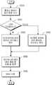
도 4는 본 본 발명의 바람직한 실시예에 따른 데이터 저장 방법의 흐름도이다.4 is a flowchart of a data storage method according to a preferred embodiment of the present invention.
USB 인터페이스 또는 SD 카드 인터페이스를 통해 데이터를 수신한다(S410). 수신된 데이터가 USB 인터페이스를 통해 수신된 데이터인지 SD 카드 인터페이스를 통해 수신된 데이터인지 판단하여(S420), USB 인터페이스를 통해 수신된 데이터이면 SCSI 변환을 수행하여 어드레스와 데이터로 분리하여 어드레스는 주소 결정부(215)로 전달하고 데이터는 DMA 제어부(225)로 전달한다(S430). 만일 SD 카드 인터페이스를 통해 수신된 데이터이면 전술한 SD 카드 명령 해석에 따라 어드레스와 데이터를 분리하여 어드레스는 주소 결정부(215)로 전달하고 데이터는 DMA 제어부(225)로 전달한다(S440). 그리고 DMA 채널의 상태에 따라 DMA 채널을 결정하고, 플래시 메모리의 기록 어드레스를 정한 후(S450), DMA를 수행한다(S460).Data is received through the USB interface or the SD card interface (S410). It is determined whether the received data is the data received through the USB interface or the data through the SD card interface (S420). If the data is received through the USB interface, SCSI conversion is performed to separate the address and the data. The data is transferred to the
도 5는 본 본 발명의 바람직한 실시예에 따른 데이터 읽기 방법의 흐름도이다.5 is a flowchart of a data reading method according to a preferred embodiment of the present invention.
USB 인터페이스 또는 SD 카드 인터페이스를 통해 플래시 메모리에 저장된 데이터를 읽는 경우에도 2개의 DMA 채널을 이용하여 읽는 속도를 높인다. 우선 USB 인터페이스 또는 SD 카드 인터페이스를 통해 플래시 메모리의 접근 명령을 수신한다(S510). USB 인터페이스를 통해 플래시 메모리를 접근한 것인지 또는 SD 카드 인터페이스를 통해 플래시 메모리를 접근하는 것인지 판단하여(S520), USB 인터페이 스를 통해 접근하는 것이면 SCSI 변환을 수행하여 어드레스와 데이터로 분리하여 어드레스는 주소 결정부(215)로 전달하고 데이터는 DMA 제어부(225)로 전달한다(S530). 마찬가지로 SD 카드 인터페이스를 통해 접근하는 경우에도 전술한 SD 카드 명령 해석에 따라 어드레스와 데이터를 분리하여 어드레스는 주소 결정부(215)로 전달하고 데이터는 DMA 제어부(225)로 전달한다(S540). 그리고 DMA 채널의 상태에 따라 DMA 채널을 결정하고, 플래시 메모리의 읽기 어드레스를 정한 후(S550), DMA를 수행한다(S560).When reading data stored in flash memory via USB interface or SD card interface, it uses two DMA channels to speed up reading. First, an access command of a flash memory is received through a USB interface or an SD card interface (S510). It is determined whether the flash memory is accessed through the USB interface or the flash memory through the SD card interface (S520). If the access is made through the USB interface, SCSI conversion is performed to separate the address and data. The data is transmitted to the
한편, 전술한 데이터 저장 및 읽기 방법은 컴퓨터 프로그램으로 작성 가능하다. 상기 프로그램을 구성하는 코드들 및 코드 세그먼트들은 당해 분야의 컴퓨터 프로그래머에 의하여 용이하게 추론될 수 있다. 또한, 상기 프로그램은 컴퓨터가 읽을 수 있는 정보저장매체(computer readable media)에 저장되고, 컴퓨터에 의하여 읽혀지고 실행됨으로써 데이터 저장 및 읽기 방법을 구현한다. 상기 정보저장매체는 자기 기록매체, 광 기록매체, 및 캐리어 웨이브 매체를 포함한다.On the other hand, the above-described data storage and reading method can be created by a computer program. Codes and code segments constituting the program can be easily inferred by a computer programmer in the art. In addition, the program is stored in a computer readable media, and read and executed by a computer to implement a data storage and reading method. The information storage medium includes a magnetic recording medium, an optical recording medium, and a carrier wave medium.
이제까지 본 발명에 대하여 그 바람직한 실시예들을 중심으로 살펴보았다. 본 발명이 속하는 기술 분야에서 통상의 지식을 가진 자는 본 발명이 본 발명의 본질적인 특성에서 벗어나지 않는 범위에서 변형된 형태로 구현될 수 있음을 이해할 수 있을 것이다. 그러므로 개시된 실시예들은 한정적인 관점이 아니라 설명적인 관점에서 고려되어야 한다. 본 발명의 범위는 전술한 설명이 아니라 특허청구범위에 나타나 있으며, 그와 동등한 범위 내에 있는 모든 차이점은 본 발명에 포함된 것으로 해석되어야 할 것이다.So far I looked at the center of the preferred embodiment for the present invention. Those skilled in the art will appreciate that the present invention can be implemented in a modified form without departing from the essential features of the present invention. Therefore, the disclosed embodiments should be considered in descriptive sense only and not for purposes of limitation. The scope of the present invention is shown in the claims rather than the foregoing description, and all differences within the scope will be construed as being included in the present invention.
전술한 바와 같이 본 발명에 따르면, USN 인터페이스 및 SD 카드 인터페이스를 모두 갖추고, DMA 채널을 복수개 구비함으로써 플래시 메모리의 데이터 읽기 및 쓰기 속도가 향상된다.As described above, according to the present invention, both the USN interface and the SD card interface are provided, and a plurality of DMA channels are provided, thereby improving data read and write speed of the flash memory.
Claims (9)
Translated fromKoreanPriority Applications (4)
| Application Number | Priority Date | Filing Date | Title |
|---|---|---|---|
| KR1020050042371AKR100725271B1 (en) | 2005-05-20 | 2005-05-20 | USB-SD storage device having a plurality of DMA channels and a storage method thereof |
| JP2008512221AJP2008547068A (en) | 2005-05-20 | 2006-05-19 | USB-SD storage device having a plurality of DMA channels, storage method thereof and recording medium |
| PCT/KR2006/001896WO2006123919A1 (en) | 2005-05-20 | 2006-05-19 | Usb-sd memory device having dma channels and method of storing data in usb-sd memory device |
| US11/915,079US20080235410A1 (en) | 2005-05-20 | 2006-05-19 | Usb-Sd Memory Device Having Dma Channels and Method of Storing Data in Usb-Sd Memory Device |
Applications Claiming Priority (1)
| Application Number | Priority Date | Filing Date | Title |
|---|---|---|---|
| KR1020050042371AKR100725271B1 (en) | 2005-05-20 | 2005-05-20 | USB-SD storage device having a plurality of DMA channels and a storage method thereof |
Publications (2)
| Publication Number | Publication Date |
|---|---|
| KR20060119391A KR20060119391A (en) | 2006-11-24 |
| KR100725271B1true KR100725271B1 (en) | 2007-06-04 |
Family
ID=37431463
Family Applications (1)
| Application Number | Title | Priority Date | Filing Date |
|---|---|---|---|
| KR1020050042371AExpired - Fee RelatedKR100725271B1 (en) | 2005-05-20 | 2005-05-20 | USB-SD storage device having a plurality of DMA channels and a storage method thereof |
Country Status (4)
| Country | Link |
|---|---|
| US (1) | US20080235410A1 (en) |
| JP (1) | JP2008547068A (en) |
| KR (1) | KR100725271B1 (en) |
| WO (1) | WO2006123919A1 (en) |
Families Citing this family (16)
| Publication number | Priority date | Publication date | Assignee | Title |
|---|---|---|---|---|
| US20080222323A1 (en)* | 2006-06-14 | 2008-09-11 | Genesys Logic, Inc. | Multimedia adapting apparatus |
| KR100823171B1 (en)* | 2007-02-01 | 2008-04-18 | 삼성전자주식회사 | Computer system with partitioned flash translation layer and partitioning method of flash translation layer |
| US20080250190A1 (en)* | 2007-04-03 | 2008-10-09 | Brian Johnson | Portable memory device operating system and method of using same |
| KR20080105390A (en)* | 2007-05-30 | 2008-12-04 | 삼성전자주식회사 | Method and apparatus for controlling instructions used in flash memory |
| KR100921748B1 (en)* | 2007-06-04 | 2009-10-15 | 삼성전자주식회사 | Memory system including ECC circuit and driving method thereof |
| US8185713B2 (en) | 2007-09-19 | 2012-05-22 | Marvell World Travel Ltd. | Flexible sequencer design architecture for solid state memory controller |
| CN101162449B (en) | 2007-10-08 | 2010-06-02 | 福州瑞芯微电子有限公司 | NAND FLASH controller and data interactive method with NAND FLASH chip |
| US7921255B2 (en)* | 2007-12-21 | 2011-04-05 | Sandisk Corporation | Duplicate SD interface memory card controller |
| KR100950936B1 (en)* | 2008-05-28 | 2010-04-01 | 주식회사 셀픽 | Solid state drive with multiple drives |
| KR101573791B1 (en)* | 2009-06-10 | 2015-12-02 | 삼성전자주식회사 | Method and apparatus for data transmission using universal serial bus |
| CN102014528B (en)* | 2010-04-28 | 2012-04-18 | 华为终端有限公司 | A wireless Internet access device, system and method |
| EP2671163B1 (en)* | 2011-02-02 | 2016-06-01 | T-Data Systems (S) Pte Ltd | A portable data storage device with wireless functionality having a digital switch circuit and a method for storing data in the aforementioned |
| WO2014116195A2 (en)* | 2012-10-31 | 2014-07-31 | Hewlett-Packard Development Company, L.P. | Writing standard tape format to memory |
| CN105988955B (en)* | 2015-02-06 | 2019-11-01 | 澜起科技股份有限公司 | SDIO equipment and its electronic device and data transmission method of application |
| CN110609661A (en)* | 2019-09-27 | 2019-12-24 | 乐普智芯(天津)医疗器械有限公司 | A kind of flash memory controller with integrated function of reading and writing |
| CN111415697B (en)* | 2020-03-20 | 2022-08-16 | 杭州华澜微电子股份有限公司 | Method, device and system for verifying flash translation layer algorithm |
Citations (2)
| Publication number | Priority date | Publication date | Assignee | Title |
|---|---|---|---|---|
| JP2001307025A (en) | 2000-04-21 | 2001-11-02 | Toshiba Corp | I / O device and electronic equipment |
| JP2003317054A (en) | 2002-04-19 | 2003-11-07 | Carry Computer Engineering Co Ltd | Double-interface sd flash memory card |
Family Cites Families (5)
| Publication number | Priority date | Publication date | Assignee | Title |
|---|---|---|---|---|
| JP3104646B2 (en)* | 1997-06-04 | 2000-10-30 | ソニー株式会社 | External storage device |
| JP2001307525A (en)* | 2000-04-21 | 2001-11-02 | Matsushita Electric Ind Co Ltd | Surface emitting device |
| JP2004220575A (en)* | 2002-12-27 | 2004-08-05 | Ricoh Co Ltd | Interface circuit for card-type memory, ASIC with the circuit, and image forming apparatus with the ASIC |
| US7062585B2 (en)* | 2003-08-21 | 2006-06-13 | Altek Corporation | Memory card for integrating the USB interface and an adaptor for the memory card |
| US7769950B2 (en)* | 2004-03-24 | 2010-08-03 | Qualcomm Incorporated | Cached memory system and cache controller for embedded digital signal processor |
- 2005
- 2005-05-20KRKR1020050042371Apatent/KR100725271B1/ennot_activeExpired - Fee Related
- 2006
- 2006-05-19WOPCT/KR2006/001896patent/WO2006123919A1/enactiveApplication Filing
- 2006-05-19USUS11/915,079patent/US20080235410A1/ennot_activeAbandoned
- 2006-05-19JPJP2008512221Apatent/JP2008547068A/enactivePending
Patent Citations (2)
| Publication number | Priority date | Publication date | Assignee | Title |
|---|---|---|---|---|
| JP2001307025A (en) | 2000-04-21 | 2001-11-02 | Toshiba Corp | I / O device and electronic equipment |
| JP2003317054A (en) | 2002-04-19 | 2003-11-07 | Carry Computer Engineering Co Ltd | Double-interface sd flash memory card |
Also Published As
| Publication number | Publication date |
|---|---|
| US20080235410A1 (en) | 2008-09-25 |
| KR20060119391A (en) | 2006-11-24 |
| WO2006123919A1 (en) | 2006-11-23 |
| JP2008547068A (en) | 2008-12-25 |
Similar Documents
| Publication | Publication Date | Title |
|---|---|---|
| CN107844431B (en) | Mapping table updating method, memory control circuit unit and memory storage device | |
| US11829601B2 (en) | Extended utilization area for a memory device | |
| US20080235410A1 (en) | Usb-Sd Memory Device Having Dma Channels and Method of Storing Data in Usb-Sd Memory Device | |
| KR101395778B1 (en) | Memory card and memory system including the same and operating method thereof | |
| KR102691851B1 (en) | Nonvolatile memory device, data storage apparatus including the same and operating method thereof | |
| US9043549B2 (en) | Memory storage apparatus, memory controller, and method for transmitting and identifying data stream | |
| TW201732597A (en) | Data storage device and operating method thereof | |
| CN113885808B (en) | Mapping information recording method, memory control circuit unit and memory device | |
| US8127072B2 (en) | Data storage device and method for accessing flash memory | |
| US20180239557A1 (en) | Nonvolatile memory device, data storage device including the same, and operating method of data storage device | |
| KR102595233B1 (en) | Data processing system and operating method thereof | |
| KR20200114212A (en) | Data storage device and operating method thereof | |
| CN111796759A (en) | Computer-readable storage medium and method for fragment data reading on multiple planes | |
| KR102695482B1 (en) | Data storage device and operating method thereof | |
| CN114328297A (en) | Mapping table management method, memory control circuit unit and memory storage device | |
| KR20200015185A (en) | Data storage device and operating method thereof | |
| KR102835936B1 (en) | Data storage device, electronic device including the same and operating method of data storage device | |
| KR100479170B1 (en) | Access control device for memory and method thereof | |
| KR101165966B1 (en) | Memory system being accessed as a synchronous mode or an asynchronous mode by command | |
| JP2009193563A (en) | System and method for protecting access of flash memory device | |
| KR102788289B1 (en) | Data storage device and operating method thereof | |
| CN110489054A (en) | Access method, relevant flash controller and the electronic device of flash memory module | |
| JPWO2008102610A1 (en) | MEMORY CONTROLLER, NONVOLATILE STORAGE DEVICE, AND NONVOLATILE STORAGE SYSTEM | |
| CN119536616A (en) | Storage system, operation method and electronic device | |
| KR101014511B1 (en) | Processor and multiple NAND flash memory access connections |
Legal Events
| Date | Code | Title | Description |
|---|---|---|---|
| A201 | Request for examination | ||
| PA0109 | Patent application | St.27 status event code:A-0-1-A10-A12-nap-PA0109 | |
| PA0201 | Request for examination | St.27 status event code:A-1-2-D10-D11-exm-PA0201 | |
| D13-X000 | Search requested | St.27 status event code:A-1-2-D10-D13-srh-X000 | |
| D14-X000 | Search report completed | St.27 status event code:A-1-2-D10-D14-srh-X000 | |
| R18-X000 | Changes to party contact information recorded | St.27 status event code:A-3-3-R10-R18-oth-X000 | |
| E701 | Decision to grant or registration of patent right | ||
| PE0701 | Decision of registration | St.27 status event code:A-1-2-D10-D22-exm-PE0701 | |
| PG1501 | Laying open of application | St.27 status event code:A-1-1-Q10-Q12-nap-PG1501 | |
| GRNT | Written decision to grant | ||
| PR0701 | Registration of establishment | St.27 status event code:A-2-4-F10-F11-exm-PR0701 | |
| PR1002 | Payment of registration fee | St.27 status event code:A-2-2-U10-U11-oth-PR1002 Fee payment year number:1 | |
| PG1601 | Publication of registration | St.27 status event code:A-4-4-Q10-Q13-nap-PG1601 | |
| PN2301 | Change of applicant | St.27 status event code:A-5-5-R10-R11-asn-PN2301 | |
| PN2301 | Change of applicant | St.27 status event code:A-5-5-R10-R14-asn-PN2301 | |
| PN2301 | Change of applicant | St.27 status event code:A-5-5-R10-R14-asn-PN2301 | |
| P14-X000 | Amendment of ip right document requested | St.27 status event code:A-5-5-P10-P14-nap-X000 | |
| P16-X000 | Ip right document amended | St.27 status event code:A-5-5-P10-P16-nap-X000 | |
| Q16-X000 | A copy of ip right certificate issued | St.27 status event code:A-4-4-Q10-Q16-nap-X000 | |
| FPAY | Annual fee payment | Payment date:20100528 Year of fee payment:4 | |
| PR1001 | Payment of annual fee | St.27 status event code:A-4-4-U10-U11-oth-PR1001 Fee payment year number:4 | |
| LAPS | Lapse due to unpaid annual fee | ||
| PC1903 | Unpaid annual fee | St.27 status event code:A-4-4-U10-U13-oth-PC1903 Not in force date:20110530 Payment event data comment text:Termination Category : DEFAULT_OF_REGISTRATION_FEE | |
| PC1903 | Unpaid annual fee | St.27 status event code:N-4-6-H10-H13-oth-PC1903 Ip right cessation event data comment text:Termination Category : DEFAULT_OF_REGISTRATION_FEE Not in force date:20110530 |