KR100724916B1 - Electronic circuit package - Google Patents
Electronic circuit packageDownload PDFInfo
- Publication number
- KR100724916B1 KR100724916B1KR1020060000219AKR20060000219AKR100724916B1KR 100724916 B1KR100724916 B1KR 100724916B1KR 1020060000219 AKR1020060000219 AKR 1020060000219AKR 20060000219 AKR20060000219 AKR 20060000219AKR 100724916 B1KR100724916 B1KR 100724916B1
- Authority
- KR
- South Korea
- Prior art keywords
- electronic
- circuit package
- electronic modules
- electronic circuit
- modules
- Prior art date
- Legal status (The legal status is an assumption and is not a legal conclusion. Google has not performed a legal analysis and makes no representation as to the accuracy of the status listed.)
- Expired - Fee Related
Links
Images


Classifications
- H—ELECTRICITY
- H01—ELECTRIC ELEMENTS
- H01L—SEMICONDUCTOR DEVICES NOT COVERED BY CLASS H10
- H01L23/00—Details of semiconductor or other solid state devices
- H01L23/552—Protection against radiation, e.g. light or electromagnetic waves
- B—PERFORMING OPERATIONS; TRANSPORTING
- B31—MAKING ARTICLES OF PAPER, CARDBOARD OR MATERIAL WORKED IN A MANNER ANALOGOUS TO PAPER; WORKING PAPER, CARDBOARD OR MATERIAL WORKED IN A MANNER ANALOGOUS TO PAPER
- B31B—MAKING CONTAINERS OF PAPER, CARDBOARD OR MATERIAL WORKED IN A MANNER ANALOGOUS TO PAPER
- B31B50/00—Making rigid or semi-rigid containers, e.g. boxes or cartons
- B31B50/60—Uniting opposed surfaces or edges; Taping
- B31B50/68—Uniting opposed surfaces or edges; Taping by stitching, stapling or riveting
- H—ELECTRICITY
- H01—ELECTRIC ELEMENTS
- H01L—SEMICONDUCTOR DEVICES NOT COVERED BY CLASS H10
- H01L25/00—Assemblies consisting of a plurality of semiconductor or other solid state devices
- H01L25/03—Assemblies consisting of a plurality of semiconductor or other solid state devices all the devices being of a type provided for in a single subclass of subclasses H10B, H10D, H10F, H10H, H10K or H10N, e.g. assemblies of rectifier diodes
- H01L25/04—Assemblies consisting of a plurality of semiconductor or other solid state devices all the devices being of a type provided for in a single subclass of subclasses H10B, H10D, H10F, H10H, H10K or H10N, e.g. assemblies of rectifier diodes the devices not having separate containers
- H01L25/065—Assemblies consisting of a plurality of semiconductor or other solid state devices all the devices being of a type provided for in a single subclass of subclasses H10B, H10D, H10F, H10H, H10K or H10N, e.g. assemblies of rectifier diodes the devices not having separate containers the devices being of a type provided for in group H10D89/00
- H01L25/0657—Stacked arrangements of devices
- H—ELECTRICITY
- H01—ELECTRIC ELEMENTS
- H01L—SEMICONDUCTOR DEVICES NOT COVERED BY CLASS H10
- H01L25/00—Assemblies consisting of a plurality of semiconductor or other solid state devices
- H01L25/16—Assemblies consisting of a plurality of semiconductor or other solid state devices the devices being of types provided for in two or more different subclasses of H10B, H10D, H10F, H10H, H10K or H10N, e.g. forming hybrid circuits
- H01L25/165—Containers
- H—ELECTRICITY
- H01—ELECTRIC ELEMENTS
- H01L—SEMICONDUCTOR DEVICES NOT COVERED BY CLASS H10
- H01L2224/00—Indexing scheme for arrangements for connecting or disconnecting semiconductor or solid-state bodies and methods related thereto as covered by H01L24/00
- H01L2224/01—Means for bonding being attached to, or being formed on, the surface to be connected, e.g. chip-to-package, die-attach, "first-level" interconnects; Manufacturing methods related thereto
- H01L2224/10—Bump connectors; Manufacturing methods related thereto
- H01L2224/15—Structure, shape, material or disposition of the bump connectors after the connecting process
- H01L2224/16—Structure, shape, material or disposition of the bump connectors after the connecting process of an individual bump connector
- H—ELECTRICITY
- H01—ELECTRIC ELEMENTS
- H01L—SEMICONDUCTOR DEVICES NOT COVERED BY CLASS H10
- H01L2225/00—Details relating to assemblies covered by the group H01L25/00 but not provided for in its subgroups
- H01L2225/03—All the devices being of a type provided for in the same main group of the same subclass of class H10, e.g. assemblies of rectifier diodes
- H01L2225/04—All the devices being of a type provided for in the same main group of the same subclass of class H10, e.g. assemblies of rectifier diodes the devices not having separate containers
- H01L2225/065—All the devices being of a type provided for in the same main group of the same subclass of class H10
- H01L2225/06503—Stacked arrangements of devices
- H01L2225/06513—Bump or bump-like direct electrical connections between devices, e.g. flip-chip connection, solder bumps
- H—ELECTRICITY
- H01—ELECTRIC ELEMENTS
- H01L—SEMICONDUCTOR DEVICES NOT COVERED BY CLASS H10
- H01L2225/00—Details relating to assemblies covered by the group H01L25/00 but not provided for in its subgroups
- H01L2225/03—All the devices being of a type provided for in the same main group of the same subclass of class H10, e.g. assemblies of rectifier diodes
- H01L2225/04—All the devices being of a type provided for in the same main group of the same subclass of class H10, e.g. assemblies of rectifier diodes the devices not having separate containers
- H01L2225/065—All the devices being of a type provided for in the same main group of the same subclass of class H10
- H01L2225/06503—Stacked arrangements of devices
- H01L2225/06527—Special adaptation of electrical connections, e.g. rewiring, engineering changes, pressure contacts, layout
- H—ELECTRICITY
- H01—ELECTRIC ELEMENTS
- H01L—SEMICONDUCTOR DEVICES NOT COVERED BY CLASS H10
- H01L24/00—Arrangements for connecting or disconnecting semiconductor or solid-state bodies; Methods or apparatus related thereto
- H01L24/01—Means for bonding being attached to, or being formed on, the surface to be connected, e.g. chip-to-package, die-attach, "first-level" interconnects; Manufacturing methods related thereto
- H01L24/10—Bump connectors ; Manufacturing methods related thereto
- H01L24/15—Structure, shape, material or disposition of the bump connectors after the connecting process
- H01L24/16—Structure, shape, material or disposition of the bump connectors after the connecting process of an individual bump connector
- H—ELECTRICITY
- H01—ELECTRIC ELEMENTS
- H01L—SEMICONDUCTOR DEVICES NOT COVERED BY CLASS H10
- H01L2924/00—Indexing scheme for arrangements or methods for connecting or disconnecting semiconductor or solid-state bodies as covered by H01L24/00
- H01L2924/10—Details of semiconductor or other solid state devices to be connected
- H01L2924/11—Device type
- H01L2924/14—Integrated circuits
- H—ELECTRICITY
- H01—ELECTRIC ELEMENTS
- H01L—SEMICONDUCTOR DEVICES NOT COVERED BY CLASS H10
- H01L2924/00—Indexing scheme for arrangements or methods for connecting or disconnecting semiconductor or solid-state bodies as covered by H01L24/00
- H01L2924/30—Technical effects
- H01L2924/301—Electrical effects
- H01L2924/3025—Electromagnetic shielding
Landscapes
- Engineering & Computer Science (AREA)
- Microelectronics & Electronic Packaging (AREA)
- Physics & Mathematics (AREA)
- Power Engineering (AREA)
- Condensed Matter Physics & Semiconductors (AREA)
- General Physics & Mathematics (AREA)
- Computer Hardware Design (AREA)
- Health & Medical Sciences (AREA)
- Electromagnetism (AREA)
- Toxicology (AREA)
- Shielding Devices Or Components To Electric Or Magnetic Fields (AREA)
Abstract
Translated fromKoreanDescription
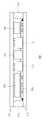
Translated fromKorean도 1은 종래 전자 회로 패키지의 구성을 나타내는 도면,1 is a view showing the configuration of a conventional electronic circuit package,
도 2는 본 발명의 제1 실시 예에 따른 전자 회로 패키지의 구성을 나타내는 도면,2 is a diagram illustrating a configuration of an electronic circuit package according to a first embodiment of the present disclosure;
도 3은 본 발명의 제2 실시 예에 따른 전자 회로 패키지의 구성을 나타내는 도면,3 is a diagram illustrating a configuration of an electronic circuit package according to a second embodiment of the present disclosure;
도 4는 본 발명의 제3 실시 예에 따른 전자 회로 패키지의 구성을 나타내는 도면,4 is a diagram illustrating a configuration of an electronic circuit package according to a third embodiment of the present disclosure;
도 5는 본 발명의 제4 실시 예에 따른 전자 회로 패키지의 구성을 나타내는 도면,5 is a diagram illustrating a configuration of an electronic circuit package according to a fourth embodiment of the present disclosure;
본 발명은 반도체 전자 회로를 포함하는 전자 회로 패키지에 관한 발명으로서, 특히 서로 다른 다수의 전자 모듈들이 집적된 전자 회로 패키지에 관한 발명이다.The present invention relates to an electronic circuit package including a semiconductor electronic circuit, and more particularly to an electronic circuit package in which a plurality of different electronic modules are integrated.
휴대용 단말기 등이 점차 소형화, 고집적화가 이루어지면서 이에 소요되는 부품도 소형화가 요구되고 있다. 소형화된 부품 수요를 충족시키기 위해서 다양한 패키지 형태의 부품 소자들이 개발되고 있으며, 특히 3D SiP(system in package) 형태가 주를 이루고 있다.As portable terminals, etc. are gradually miniaturized and highly integrated, components required for them are also required to be miniaturized. In order to meet the demand for miniaturized components, various packaged component devices are being developed, especially 3D system in package (SiP).
도 1은 종래 전자 회로 패키지를 도시한 도면이다. 종래 전자 회로 패키지(100)는 보드(110)와, 상기 보드 상에 형성된 칩셋(chip set;120)과, 상기 칩셋(120) 상에 형성된 다중 칩 패키지(multi chip package;130)를 포함한다. 상술한 다중 칩 패키지(130)는 통상 POP(Package on package) 방식이 적용되고 있다.1 is a diagram illustrating a conventional electronic circuit package. The conventional
그러나, 3D 형태의 SIP 부품은 고주파 신호의 간섭에 의한 특성 저하와, 시그널 인터그리티(Signal integrity)가 확보되지 못하는 문제가 있다. 더욱이, 고주파 혼합 신호를 다루는 통신 모듈은 송신 및 수신 단에서 간섭 현상의 발생으로 인해 신호의 송신 및 수신시 오류가 발생하는 문제가 있다.However, the 3D SIP component has problems of deterioration of characteristics due to interference of high frequency signals and inability to secure signal integrity. Moreover, a communication module dealing with a high frequency mixed signal has a problem that an error occurs in transmitting and receiving signals due to the occurrence of interference at the transmitting and receiving ends.
본 발명은 송신 및 수신 신호의 상호 간섭을 억제하고, 다수의 회로들을 집적시킬 수 있는 소형화된 전자 회로 패키지를 제공하는 데 목적이 있다.It is an object of the present invention to provide a miniaturized electronic circuit package capable of suppressing mutual interference of transmitted and received signals and integrating multiple circuits.
본 발명에 따른 전자회로 패키지는,An electronic circuit package according to the present invention,
집적된 소자들이 상호 대면하도록 접합된 제1 및 제2 전자 모듈들과;First and second electronic modules bonded together so that the integrated devices face each other;
상기 전자 모듈들 사이에 삽입되며 상기 제1 및 제2 전자 모듈들 사이의 전기적 절연을 확보하기 위한 전기 실드 막을 포함한다.And an electrical shield film inserted between the electronic modules to secure electrical insulation between the first and second electronic modules.
이하에서는 첨부도면들을 참조하여 본 발명의 실시 예를 상세히 설명하기로 한다. 본 발명을 설명함에 있어서, 관련된 공지기능, 혹은 구성에 대한 구체적인 설명은 본 발명의 요지를 모호하지 않게 하기 위하여 생략한다.Hereinafter, with reference to the accompanying drawings will be described an embodiment of the present invention; In describing the present invention, detailed descriptions of related well-known functions or configurations are omitted in order not to obscure the subject matter of the present invention.
도 2는 본 발명의 제1 실시 예에 따른 전자 회로 패키지의 구성을 나타내는 도면이다. 도 2를 참조하면, 본 실시 예에 따른 전자 회로 패키지(200)는 집적된 소자들(211,212,221,222)이 상호 대면하도록 접합된 제1 및 제2 전자 모듈들(210,220)과, 상기 제1 및 제2 전자 모듈들(210,220) 사이에 삽입되며 상기 제1 및 제2 전자 모듈들(210,220) 사이의 전기적 절연을 확보하기 위한 전기 실드 막(230)과, 신호 연결 및 접지 핀들(241,242)을 포함한다.2 is a diagram illustrating a configuration of an electronic circuit package according to a first embodiment of the present invention. Referring to FIG. 2, the
상기 전기 실드 막(230)은 자기 방지 접지 면(Magnetic Shielding Ground Plane)이 사용될 수 있으며, 서로 다른 고주파 신호(RF)를 사용하는 전자 모듈들의 집적에 있어서 고주파 신호들이 상호 간섭되는 것을 방지함으로써 고집적, 낮은 프로파일(Low profile)의 모듈들이 집적된 3차원 구조의 전자 회로 패키지 구현이 가능할 수 있도록 한다.Magnetic shielding ground plane (Magnetic Shielding Ground Plane) may be used as the
상기 신호 연결핀들(241)은 상기 제1 및 제2 전자 모듈(210,220) 사이의 일측 끝단에 삽입되며 상기 제1 전자 모듈(210)과 상기 제2 전자 모듈 사이(220)를 전기적으로 연결시키며, 둘 이상의 다수가 사용될 수 있다. 상기 접지 핀(242)은 상기 제1 및 제2 전자 모듈(210,220) 사이의 일측 끝단에 삽입되며 상기 제1 및 제2 전자 모듈(210,220)의 전기적 접지를 형성한다. 상기 신호 연결 및 접지 핀들 (241,242)은 솔더 볼(solder-ball)에 의해 형성될 수 있다.The
도 3은 본 발명의 제2 실시 예에 따른 전자 회로 패키지의 구성을 나타내는 도면이다. 도 3을 참조하면, 본 실시 예에 따른 전자 회로 패키지(300)는 집적된 소자들(311,312,321,322)이 상호 대면하도록 접합된 제1 및 제2 전자 모듈들(310,320)과, 상기 제1 및 제2 전자 모듈들(310,320) 사이에 삽입되며 상기 제1 및 제2 전자 모듈들(310,320) 사이의 전기적 절연을 확보하기 위한 전기 실드 막(330)과, 신호 연결 및 접지 핀들(341a,341b,342a,342b)을 포함한다.3 is a diagram illustrating a configuration of an electronic circuit package according to a second embodiment of the present invention. Referring to FIG. 3, the
상기 신호 연결핀들(341a,341b)은 상기 제1 및 제2 전자 모듈(310,320) 사이의 일측 끝단에 삽입되며 상기 제1 전자 모듈(310)과 상기 제2 전자 모듈(320) 사이를 전기적으로 연결시키며, 둘 이상의 다수가 사용될 수 있다. 상기 접지 핀(342a,342b)은 상기 제1 및 제2 전자 모듈(310,320) 사이의 일측 끝단에 삽입되며 상기 제1 및 제2 전자 모듈(310,320)의 전기적 접지를 형성한다. 상기 신호 연결핀들(341a,341b)과, 상기 접지 핀들(342a,342b)은 마이크로 소켓(Micro socket)이 사용될 수 있다.The
도 4는 본 발명의 제3 실시 예에 따른 전자 회로 패키지의 구성을 나타내는 도면이다. 도 4를 참조하면, 본 실시 예에 따른 전자 회로 패키지(400)는 집적된 소자들(411,412,421,422)이 상호 대면하도록 접합된 제1 및 제2 전자 모듈들(410,420)과, 상기 제1 및 제2 전자 모듈들(410,420) 사이에 삽입되며 상기 제1 및 제2 전자 모듈들(410,420) 사이의 전기적 절연을 확보하기 위한 전기 실드 막(430)과, 신호 연결 및 접지 핀들(441a,441b,442a,442b)을 포함한다. 상기 신호 연결 및 접지 핀들(441a,441b,442a,442b)은 마이크로 소켓이 사용될 수 있다.4 is a diagram illustrating a configuration of an electronic circuit package according to a third embodiment of the present invention. Referring to FIG. 4, the
상기 전기 실드 막(430)은 일부 소자(411,412,422)를 제외한 나머지 소자들(421,423)을 차폐시키는 형태로 사용될 수 있다.The
도 5는 본 발명의 제4 실시 예에 따른 전자 회로 패키지의 구성을 나타내는 도면이다. 도 5를 참조하면, 본 실시 예에 따른 전자 회로 패키지(500)는 집적된 소자들(511,512,521,522)이 상호 대면하도록 접합된 제1 및 제2 전자 모듈들(510,520)과, 상기 제1 및 제2 전자 모듈들(510,520) 사이에 삽입되며 상기 제1 및 제2 전자 모듈들(510,520) 사이의 전기적 절연을 확보하기 위한 전기 실드 막(530)과, 신호 연결 및 접지 핀들(541,542)을 포함한다. 상기 신호 연결 및 접지 핀들(541,542)은 솔더 볼에 의해 형성될 수 있다.5 is a diagram illustrating a configuration of an electronic circuit package according to a fourth embodiment of the present invention. Referring to FIG. 5, the
상기 전기 실드 막(530)은 일부 소자(511,512,522)를 제외한 나머지 소자들(521,523)을 차폐시키는 형태로 사용될 수 있다.The
본 발명은 신호 간섭이 우려되는 서브-모듈 기판(Sub-module board), RF 부품, 수동소자, 디지털 집적회로 등의 부품 등에 적용될 수 있다.The present invention can be applied to components such as sub-module boards, RF components, passive components, digital integrated circuits, and the like, in which signal interference is concerned.
본 발명은 소자가 집적된 면이 대면하도록 전자 모듈들을 배치하고, 전자 모듈들 사이에 전기 실드를 형성함으로써, 고주파 신호 간섭의 발생을 억제할 수 있다. 따라서, 본 발명은 고집적/고성능의 RF 혼합 신호를 사용하는 RF용 전자회로 패키지에 적용될 수 있다.The present invention can suppress the occurrence of high frequency signal interference by arranging the electronic modules so that the surface where the elements are integrated face each other, and forming an electrical shield between the electronic modules. Accordingly, the present invention can be applied to an electronic circuit package for RF that uses a highly integrated / high performance RF mixed signal.
Claims (4)
Translated fromKoreanPriority Applications (2)
| Application Number | Priority Date | Filing Date | Title |
|---|---|---|---|
| KR1020060000219AKR100724916B1 (en) | 2006-01-02 | 2006-01-02 | Electronic circuit package |
| US11/618,954US7365992B2 (en) | 2006-01-02 | 2007-01-02 | Electronic circuit package |
Applications Claiming Priority (1)
| Application Number | Priority Date | Filing Date | Title |
|---|---|---|---|
| KR1020060000219AKR100724916B1 (en) | 2006-01-02 | 2006-01-02 | Electronic circuit package |
Publications (1)
| Publication Number | Publication Date |
|---|---|
| KR100724916B1true KR100724916B1 (en) | 2007-06-04 |
Family
ID=38224138
Family Applications (1)
| Application Number | Title | Priority Date | Filing Date |
|---|---|---|---|
| KR1020060000219AExpired - Fee RelatedKR100724916B1 (en) | 2006-01-02 | 2006-01-02 | Electronic circuit package |
Country Status (2)
| Country | Link |
|---|---|
| US (1) | US7365992B2 (en) |
| KR (1) | KR100724916B1 (en) |
Cited By (1)
| Publication number | Priority date | Publication date | Assignee | Title |
|---|---|---|---|---|
| KR101873407B1 (en) | 2011-07-13 | 2018-07-02 | 엘지전자 주식회사 | Mobile terminal |
Families Citing this family (14)
| Publication number | Priority date | Publication date | Assignee | Title |
|---|---|---|---|---|
| US7729131B2 (en)* | 2007-01-05 | 2010-06-01 | Apple Inc. | Multiple circuit board arrangements in electronic devices |
| CN101982027A (en)* | 2008-03-24 | 2011-02-23 | 松下电器产业株式会社 | Electronic circuit board and power line communication device using the same |
| FR2951019B1 (en) | 2009-10-07 | 2012-06-08 | Valeo Etudes Electroniques | POWER MODULE FOR MOTOR VEHICLE |
| JP2014045042A (en)* | 2012-08-24 | 2014-03-13 | Fujitsu Ltd | Mounting structure and electronic apparatus |
| US9363892B2 (en) | 2013-07-19 | 2016-06-07 | Google Technology Holdings LLC | Circuit assembly and corresponding methods |
| CN104267791B (en)* | 2014-10-24 | 2018-08-28 | 江西创成电子有限公司 | A kind of Portable tablet personal computer |
| US9986639B2 (en)* | 2015-06-29 | 2018-05-29 | Analog Devices Global | Vertical magnetic barrier for integrated electronic module and related methods |
| JP6780422B2 (en)* | 2016-09-30 | 2020-11-04 | オムロン株式会社 | Electronics |
| KR102493356B1 (en)* | 2018-06-19 | 2023-01-31 | 삼성전자주식회사 | A structure in which another circuit board is disposed on the upper surface of the shield can disposed on a circuit board, and electronic device with the same |
| US11032953B2 (en) | 2019-04-25 | 2021-06-08 | Microsoft Technology Licensing, Llc | Mutually shielded printed circuit board assembly |
| WO2020250795A1 (en)* | 2019-06-10 | 2020-12-17 | 株式会社ライジングテクノロジーズ | Electronic circuit device |
| US11258356B2 (en) | 2019-07-31 | 2022-02-22 | Analog Devices International Unlimited Company | Magnetic barrier for power module |
| KR102719956B1 (en)* | 2020-02-07 | 2024-10-22 | 삼성전자주식회사 | An electronic device comprising a mmwave antenna module |
| CN113365411B (en)* | 2020-03-03 | 2025-09-19 | 深南电路股份有限公司 | Embedded electronic device and manufacturing method thereof |
Citations (2)
| Publication number | Priority date | Publication date | Assignee | Title |
|---|---|---|---|---|
| KR20020092961A (en)* | 2000-02-18 | 2002-12-12 | 인세프 테크놀러지스, 인코포레이티드 | Method and apparatus for providing power to a microprocessor with integrated thermal and emi management |
| KR20050120146A (en)* | 2004-06-18 | 2005-12-22 | 삼성테크윈 주식회사 | Electronic-circuit module package |
Family Cites Families (11)
| Publication number | Priority date | Publication date | Assignee | Title |
|---|---|---|---|---|
| JPH036099A (en)* | 1989-06-02 | 1991-01-11 | Canon Inc | Mounting structure of electronic equipment |
| FI117224B (en)* | 1994-01-20 | 2006-07-31 | Nec Tokin Corp | Electromagnetic interference suppression piece, applied by electronic device and hybrid integrated circuit element |
| US5777856A (en)* | 1996-08-06 | 1998-07-07 | Motorola, Inc. | Integrated shielding and mechanical support |
| JP4366863B2 (en)* | 2000-02-02 | 2009-11-18 | 株式会社デンソー | Electronic control unit |
| DE10026353A1 (en)* | 2000-05-27 | 2001-11-29 | Mannesmann Vdo Ag | Shielded electronic circuit |
| US6674652B2 (en)* | 2002-01-29 | 2004-01-06 | 3Com Corporation | Integrated shield wrap |
| US6574103B1 (en)* | 2002-03-08 | 2003-06-03 | Lucent Technologies Inc. | Enclosure with RF isolation for circuit packs |
| US7161092B2 (en)* | 2002-04-15 | 2007-01-09 | Visteon Global Technologies, Inc. | Apparatus and method for protecting an electronic circuit |
| US6621708B1 (en)* | 2002-06-10 | 2003-09-16 | Sun Microsystems, Inc. | Electronics assembly including a protective shield |
| US6972967B2 (en)* | 2003-02-20 | 2005-12-06 | Avaya Technology Group | EMC/ESD mitigation module |
| JP4037810B2 (en)* | 2003-09-05 | 2008-01-23 | Necアクセステクニカ株式会社 | Small wireless device and mounting method thereof |
- 2006
- 2006-01-02KRKR1020060000219Apatent/KR100724916B1/ennot_activeExpired - Fee Related
- 2007
- 2007-01-02USUS11/618,954patent/US7365992B2/ennot_activeExpired - Fee Related
Patent Citations (2)
| Publication number | Priority date | Publication date | Assignee | Title |
|---|---|---|---|---|
| KR20020092961A (en)* | 2000-02-18 | 2002-12-12 | 인세프 테크놀러지스, 인코포레이티드 | Method and apparatus for providing power to a microprocessor with integrated thermal and emi management |
| KR20050120146A (en)* | 2004-06-18 | 2005-12-22 | 삼성테크윈 주식회사 | Electronic-circuit module package |
Cited By (1)
| Publication number | Priority date | Publication date | Assignee | Title |
|---|---|---|---|---|
| KR101873407B1 (en) | 2011-07-13 | 2018-07-02 | 엘지전자 주식회사 | Mobile terminal |
Also Published As
| Publication number | Publication date |
|---|---|
| US7365992B2 (en) | 2008-04-29 |
| US20070153491A1 (en) | 2007-07-05 |
Similar Documents
| Publication | Publication Date | Title |
|---|---|---|
| US7365992B2 (en) | Electronic circuit package | |
| TWI719131B (en) | Integrated circuit device assembly, computer platform and method of assembling printed circuit assembly | |
| US9576865B2 (en) | Film for semiconductor package, semiconductor package using film and display device including the same | |
| CN106797098B (en) | Socket contact technology and construction | |
| US11304299B2 (en) | Board to board interconnect | |
| US9119320B2 (en) | System in package assembly | |
| US6426877B1 (en) | Semiconductor device incorporating module structure | |
| US20070138619A1 (en) | Semiconductor device, and inspection method thereof | |
| JP4947054B2 (en) | Socket and module board and inspection system using the same | |
| WO2013107305A1 (en) | Integrated module, integrated system board and electronic device | |
| US8379406B2 (en) | Package and method for manufacturing the same | |
| JP2000088921A (en) | Semiconductor device | |
| US10290589B2 (en) | Folding thin systems | |
| KR20130011984A (en) | Double-sided flip chip package | |
| US9370097B2 (en) | Package substrate with testing pads on fine pitch traces | |
| US9633950B1 (en) | Integrated device comprising flexible connector between integrated circuit (IC) packages | |
| WO2019123995A1 (en) | Electronic component | |
| US8872338B2 (en) | Trace routing within a semiconductor package substrate | |
| CN102469687B (en) | circuit board | |
| US20090032922A1 (en) | Semiconductor Package, Printed Wiring Board Structure and Electronic Apparatus | |
| WO2025194908A1 (en) | Packaging structure, electronic device, and method for preparing packaging structure | |
| KR20150057838A (en) | Electronic device module | |
| KR100318934B1 (en) | Printed circuit board for portable radiotelephone | |
| KR20090080702A (en) | Memory modules | |
| JP2005311066A (en) | Electronic device and its manufacturing method |
Legal Events
| Date | Code | Title | Description |
|---|---|---|---|
| A201 | Request for examination | ||
| PA0109 | Patent application | St.27 status event code:A-0-1-A10-A12-nap-PA0109 | |
| PA0201 | Request for examination | St.27 status event code:A-1-2-D10-D11-exm-PA0201 | |
| E902 | Notification of reason for refusal | ||
| PE0902 | Notice of grounds for rejection | St.27 status event code:A-1-2-D10-D21-exm-PE0902 | |
| P11-X000 | Amendment of application requested | St.27 status event code:A-2-2-P10-P11-nap-X000 | |
| P13-X000 | Application amended | St.27 status event code:A-2-2-P10-P13-nap-X000 | |
| E701 | Decision to grant or registration of patent right | ||
| PE0701 | Decision of registration | St.27 status event code:A-1-2-D10-D22-exm-PE0701 | |
| GRNT | Written decision to grant | ||
| PR0701 | Registration of establishment | St.27 status event code:A-2-4-F10-F11-exm-PR0701 | |
| PR1002 | Payment of registration fee | St.27 status event code:A-2-2-U10-U11-oth-PR1002 Fee payment year number:1 | |
| PG1601 | Publication of registration | St.27 status event code:A-4-4-Q10-Q13-nap-PG1601 | |
| PR1001 | Payment of annual fee | St.27 status event code:A-4-4-U10-U11-oth-PR1001 Fee payment year number:4 | |
| PR1001 | Payment of annual fee | St.27 status event code:A-4-4-U10-U11-oth-PR1001 Fee payment year number:5 | |
| PR1001 | Payment of annual fee | St.27 status event code:A-4-4-U10-U11-oth-PR1001 Fee payment year number:6 | |
| R18-X000 | Changes to party contact information recorded | St.27 status event code:A-5-5-R10-R18-oth-X000 | |
| FPAY | Annual fee payment | Payment date:20130429 Year of fee payment:7 | |
| PR1001 | Payment of annual fee | St.27 status event code:A-4-4-U10-U11-oth-PR1001 Fee payment year number:7 | |
| FPAY | Annual fee payment | Payment date:20140429 Year of fee payment:8 | |
| PR1001 | Payment of annual fee | St.27 status event code:A-4-4-U10-U11-oth-PR1001 Fee payment year number:8 | |
| FPAY | Annual fee payment | Payment date:20150429 Year of fee payment:9 | |
| PR1001 | Payment of annual fee | St.27 status event code:A-4-4-U10-U11-oth-PR1001 Fee payment year number:9 | |
| FPAY | Annual fee payment | Payment date:20160428 Year of fee payment:10 | |
| PR1001 | Payment of annual fee | St.27 status event code:A-4-4-U10-U11-oth-PR1001 Fee payment year number:10 | |
| FPAY | Annual fee payment | Payment date:20170427 Year of fee payment:11 | |
| PR1001 | Payment of annual fee | St.27 status event code:A-4-4-U10-U11-oth-PR1001 Fee payment year number:11 | |
| LAPS | Lapse due to unpaid annual fee | ||
| PC1903 | Unpaid annual fee | St.27 status event code:A-4-4-U10-U13-oth-PC1903 Not in force date:20180529 Payment event data comment text:Termination Category : DEFAULT_OF_REGISTRATION_FEE | |
| PC1903 | Unpaid annual fee | St.27 status event code:N-4-6-H10-H13-oth-PC1903 Ip right cessation event data comment text:Termination Category : DEFAULT_OF_REGISTRATION_FEE Not in force date:20180529 |