KR100722096B1 - Portable display - Google Patents
Portable displayDownload PDFInfo
- Publication number
- KR100722096B1 KR100722096B1KR1020050112568AKR20050112568AKR100722096B1KR 100722096 B1KR100722096 B1KR 100722096B1KR 1020050112568 AKR1020050112568 AKR 1020050112568AKR 20050112568 AKR20050112568 AKR 20050112568AKR 100722096 B1KR100722096 B1KR 100722096B1
- Authority
- KR
- South Korea
- Prior art keywords
- printed circuit
- circuit board
- liquid crystal
- display panel
- crystal display
- Prior art date
- Legal status (The legal status is an assumption and is not a legal conclusion. Google has not performed a legal analysis and makes no representation as to the accuracy of the status listed.)
- Expired - Fee Related
Links
Images


Classifications
- G—PHYSICS
- G02—OPTICS
- G02F—OPTICAL DEVICES OR ARRANGEMENTS FOR THE CONTROL OF LIGHT BY MODIFICATION OF THE OPTICAL PROPERTIES OF THE MEDIA OF THE ELEMENTS INVOLVED THEREIN; NON-LINEAR OPTICS; FREQUENCY-CHANGING OF LIGHT; OPTICAL LOGIC ELEMENTS; OPTICAL ANALOGUE/DIGITAL CONVERTERS
- G02F1/00—Devices or arrangements for the control of the intensity, colour, phase, polarisation or direction of light arriving from an independent light source, e.g. switching, gating or modulating; Non-linear optics
- G02F1/01—Devices or arrangements for the control of the intensity, colour, phase, polarisation or direction of light arriving from an independent light source, e.g. switching, gating or modulating; Non-linear optics for the control of the intensity, phase, polarisation or colour
- G02F1/13—Devices or arrangements for the control of the intensity, colour, phase, polarisation or direction of light arriving from an independent light source, e.g. switching, gating or modulating; Non-linear optics for the control of the intensity, phase, polarisation or colour based on liquid crystals, e.g. single liquid crystal display cells
- G02F1/133—Constructional arrangements; Operation of liquid crystal cells; Circuit arrangements
- G02F1/1333—Constructional arrangements; Manufacturing methods
- H—ELECTRICITY
- H05—ELECTRIC TECHNIQUES NOT OTHERWISE PROVIDED FOR
- H05K—PRINTED CIRCUITS; CASINGS OR CONSTRUCTIONAL DETAILS OF ELECTRIC APPARATUS; MANUFACTURE OF ASSEMBLAGES OF ELECTRICAL COMPONENTS
- H05K1/00—Printed circuits
- H05K1/02—Details
- H05K1/0213—Electrical arrangements not otherwise provided for
- H05K1/0254—High voltage adaptations; Electrical insulation details; Overvoltage or electrostatic discharge protection ; Arrangements for regulating voltages or for using plural voltages
- H05K1/0257—Overvoltage protection
- H05K1/0259—Electrostatic discharge [ESD] protection
- G—PHYSICS
- G02—OPTICS
- G02F—OPTICAL DEVICES OR ARRANGEMENTS FOR THE CONTROL OF LIGHT BY MODIFICATION OF THE OPTICAL PROPERTIES OF THE MEDIA OF THE ELEMENTS INVOLVED THEREIN; NON-LINEAR OPTICS; FREQUENCY-CHANGING OF LIGHT; OPTICAL LOGIC ELEMENTS; OPTICAL ANALOGUE/DIGITAL CONVERTERS
- G02F1/00—Devices or arrangements for the control of the intensity, colour, phase, polarisation or direction of light arriving from an independent light source, e.g. switching, gating or modulating; Non-linear optics
- G02F1/01—Devices or arrangements for the control of the intensity, colour, phase, polarisation or direction of light arriving from an independent light source, e.g. switching, gating or modulating; Non-linear optics for the control of the intensity, phase, polarisation or colour
- G02F1/13—Devices or arrangements for the control of the intensity, colour, phase, polarisation or direction of light arriving from an independent light source, e.g. switching, gating or modulating; Non-linear optics for the control of the intensity, phase, polarisation or colour based on liquid crystals, e.g. single liquid crystal display cells
- G02F1/133—Constructional arrangements; Operation of liquid crystal cells; Circuit arrangements
- G02F1/1333—Constructional arrangements; Manufacturing methods
- G02F1/1345—Conductors connecting electrodes to cell terminals
- G02F1/13452—Conductors connecting driver circuitry and terminals of panels
- H—ELECTRICITY
- H05—ELECTRIC TECHNIQUES NOT OTHERWISE PROVIDED FOR
- H05K—PRINTED CIRCUITS; CASINGS OR CONSTRUCTIONAL DETAILS OF ELECTRIC APPARATUS; MANUFACTURE OF ASSEMBLAGES OF ELECTRICAL COMPONENTS
- H05K1/00—Printed circuits
- H05K1/02—Details
- H05K1/0213—Electrical arrangements not otherwise provided for
- H05K1/0215—Grounding of printed circuits by connection to external grounding means
- G—PHYSICS
- G02—OPTICS
- G02F—OPTICAL DEVICES OR ARRANGEMENTS FOR THE CONTROL OF LIGHT BY MODIFICATION OF THE OPTICAL PROPERTIES OF THE MEDIA OF THE ELEMENTS INVOLVED THEREIN; NON-LINEAR OPTICS; FREQUENCY-CHANGING OF LIGHT; OPTICAL LOGIC ELEMENTS; OPTICAL ANALOGUE/DIGITAL CONVERTERS
- G02F1/00—Devices or arrangements for the control of the intensity, colour, phase, polarisation or direction of light arriving from an independent light source, e.g. switching, gating or modulating; Non-linear optics
- G02F1/01—Devices or arrangements for the control of the intensity, colour, phase, polarisation or direction of light arriving from an independent light source, e.g. switching, gating or modulating; Non-linear optics for the control of the intensity, phase, polarisation or colour
- G02F1/13—Devices or arrangements for the control of the intensity, colour, phase, polarisation or direction of light arriving from an independent light source, e.g. switching, gating or modulating; Non-linear optics for the control of the intensity, phase, polarisation or colour based on liquid crystals, e.g. single liquid crystal display cells
- G02F1/133—Constructional arrangements; Operation of liquid crystal cells; Circuit arrangements
- G02F1/1333—Constructional arrangements; Manufacturing methods
- G02F1/133308—Support structures for LCD panels, e.g. frames or bezels
- H—ELECTRICITY
- H05—ELECTRIC TECHNIQUES NOT OTHERWISE PROVIDED FOR
- H05K—PRINTED CIRCUITS; CASINGS OR CONSTRUCTIONAL DETAILS OF ELECTRIC APPARATUS; MANUFACTURE OF ASSEMBLAGES OF ELECTRICAL COMPONENTS
- H05K2201/00—Indexing scheme relating to printed circuits covered by H05K1/00
- H05K2201/05—Flexible printed circuits [FPCs]
- H05K2201/053—Tails
- H—ELECTRICITY
- H05—ELECTRIC TECHNIQUES NOT OTHERWISE PROVIDED FOR
- H05K—PRINTED CIRCUITS; CASINGS OR CONSTRUCTIONAL DETAILS OF ELECTRIC APPARATUS; MANUFACTURE OF ASSEMBLAGES OF ELECTRICAL COMPONENTS
- H05K2201/00—Indexing scheme relating to printed circuits covered by H05K1/00
- H05K2201/05—Flexible printed circuits [FPCs]
- H05K2201/055—Folded back on itself
Landscapes
- Physics & Mathematics (AREA)
- Nonlinear Science (AREA)
- Engineering & Computer Science (AREA)
- Microelectronics & Electronic Packaging (AREA)
- Mathematical Physics (AREA)
- Chemical & Material Sciences (AREA)
- Crystallography & Structural Chemistry (AREA)
- General Physics & Mathematics (AREA)
- Optics & Photonics (AREA)
- Liquid Crystal (AREA)
- Devices For Indicating Variable Information By Combining Individual Elements (AREA)
Abstract
Translated fromKoreanDescription
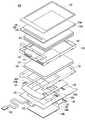
Translated fromKorean도 1은 종래의 휴대용 표시장치를 나타내는 분해 사시도이다.1 is an exploded perspective view illustrating a conventional portable display device.
도 2는 본 발명의 실시예에 의한 휴대용 표시장치를 나타내는 분해 사시도이다.2 is an exploded perspective view illustrating a portable display device according to an exemplary embodiment of the present invention.
도 3은 도 2에 도시된 돌출부와 바텀 섀시의 접촉과정을 상세히 나타내는 도면이다.3 is a view illustrating in detail the contact process of the protrusion and the bottom chassis shown in FIG.
<도면의 주요 부분에 대한 부호의 설명><Explanation of symbols for the main parts of the drawings>
2,102 : 탑 섀시4,104 : 액정 표시패널2,102: top chassis 4,104: liquid crystal display panel
4a,4b,104a,104b : 기판6,34,106 : 집적회로4a, 4b, 104a, 104b:
8,108 : 보호층10,20,110,120 : 광학 시트8,108:
12,112 : 발광 다이오드14,114 : 발광 다이오드 기판12,112: light emitting diodes 14,114: light emitting diode substrate
16,116 : 몰드 프레임18,118 : 도광판16,116: mold frame 18,118: light guide plate
20 : 반사판22,122 : 바텀 섀시20: reflector 22122: bottom chassis
24,26,32,124,126,132 : 인쇄회로기판 28,128 : 커넥터24, 26, 32, 124, 126, 132:
30,130 : 발광 표시패널 36,38,136,138 : 패드부30,130: light
40a,40b : 도전성 테이프50,150 : 백라이트 어셈블리40a, 40b:
60,160 : 액정 표시장치140a,140b : 돌출부60,160:
142a,142b : 동막142a, 142b: copper film
본 발명은 휴대용 표시장치에 관한 것으로, 특히 인쇄회로기판이 접지될 때 도전저항을 감소시킴과 동시에 제조비용을 절감할 수 있도록 한 휴대용 표시장치에 관한 것이다.BACKGROUND OF THE INVENTION 1. Field of the Invention [0001] The present invention relates to a portable display device, and more particularly, to a portable display device that can reduce manufacturing resistance and reduce conductive resistance when a printed circuit board is grounded.
최근, 음극선관(Cathode Ray Tube)의 단점인 무게와 부피를 줄일 수 있는 각종 평판 표시장치들이 개발되고 있다. 평판 표시장치로는 액정 표시장치(Liquid Crystal Display), 전계방출 표시장치(Field Emission Display), 플라즈마 표시패널(Plasma Display Panel) 및 발광 표시장치(Organic Light Emitting Display) 등이 있다.Recently, various flat panel displays have been developed to reduce weight and volume, which are disadvantages of cathode ray tubes. The flat panel display includes a liquid crystal display, a field emission display, a plasma display panel, and an organic light emitting display.
여기서, 액정 표시장치 및 발광 표시장치는 소형화, 경량화 및 저전력 등의 이점을 가지고 있어서 기존의 음극선관의 단점을 극복할 수 있는 대체 수단으로서 점차 주목받아 왔고, 현재는 핸드폰 및 PDA(Portable digital assistor) 등의 휴대용 기기뿐만 아니라 중대형 제품인 모니터 및 TV등에도 장착되고 있다.Here, the liquid crystal display and the light emitting display have been attracting attention as an alternative means to overcome the disadvantages of the conventional cathode ray tube because it has the advantages of miniaturization, light weight and low power, and now mobile phones and PDA (Portable digital assistor) In addition to portable devices, such as monitors and TVs are installed in medium and large products.
도 1은 종래의 휴대용 표시장치를 나타내는 분해 사시도이다. 도 1에서는 핸드폰 등에 사용되는 듀얼(dual) 표시장치를 도시하였다.1 is an exploded perspective view illustrating a conventional portable display device. 1 illustrates a dual display device used in a mobile phone or the like.
도 1을 참조하면, 종래의 휴대용 표시장치(60)는 탑 섀시(top chassis)(2), 액정 표시패널(4), 백라이트 어셈블리(50), 바텀 섀시(bottom chassis)(22), 제 1인쇄회로기판(24), 제 2인쇄회로기판(26) 및 발광 표시패널(30)을 구비한다.Referring to FIG. 1, a conventional
액정 표시패널(4)은 소정의 화상을 표시한다. 이를 위해, 제 1액정 표시패널(4)은 제 1기판(4a), 제 2기판(4b) 및 이들 사이에 주입되는 액정(미도시)을 구비한다.The liquid
제 2기판(4b)은 매트릭스 형태로 배치되는 다수의 박막 트랜지스터(Thin Film Transistor : 이하 "TFT"라 함)를 포함한다. 여기서, TFT의 소오스전극은 데이터선에 접속되고, 게이트전극은 주사선에 연결된다. 그리고, TFT의 드레인전극은 도전성 재질로 투명한 ITO(indium tin oxide)로 이루어진 화소전극과 접속된다. 이와같은 TFT는 주사선으로 주사신호가 공급될 때 턴-온되어 데이터선으로부터 공급되는 데이터신호를 화소전극으로 공급한다.The
이를 위해, 제 2기판(4b)의 일측에는 집적회로(6)가 삽입되고, 이 집적회로(6)로부터 데이터신호 및 주사신호가 공급된다. 그리고, 집적회로(6)의 주위에는 보호층(8)이 도포된다.To this end, an integrated circuit 6 is inserted into one side of the
제 1기판(4a)은 제 2기판(4b)과 대향되게 배치된다. 이와 같은 제 1기판(4a)의 전면에는 ITO로 이루어진 공통전극이 도포된다. 공통전극에는 소정의 전압이 인가되고, 이에 따라 공통전극과 화소전극 사이에는 소정의 전계가 형성된다. 이러한, 전계에 의해 제 1기판(4a) 및 제 2기판(4b) 사이에 주입된 액정의 배열각이 변화되고, 변화된 배열각에 따라서 광투과도가 변경되어 원하는 화상을 표시한다.The
백라이트 어셈블리(50)는 몰드 프레임(16), 발광 다이오드들(12), 발광 다이오드 기판(14), 도광판(18), 반사판(20) 및 광학 시트들(10)을 구비한다.The
발광 다이오드들(12)은 발광 다이오드 기판(14)으로부터의 구동신호에 대응하여 소정 휘도의 광을 생성한다.The light emitting diodes 12 generate light having a predetermined brightness in response to a driving signal from the light
도광판(18)은 발광 다이오드들(12)로부터 공급되는 광을 액정 표시패널(4) 로 공급한다. 즉, 도광판(18)은 자신의 측면에서 공급된 광을 자신의 상부에 위치되는 액정 표시패널(4)로 공급한다.The
반사판(20)은 도광판(18)의 배면에 위치되어 도광판(18)으로부터 입사되는 광을 도광판(18)으로 재공급한다. 즉, 반사판(20)은 자신에게 입사되는 광을 도광판(18)으로 재공급함으로써 광 효율을 향상시키게 된다.The reflecting
제 1광학시트들(10)은 도광판(18)으로부터 공급된 광의 휘도 등을 향상시켜 액정 표시패널(4)로 공급한다.The first
발광 다이오드 기판(14)은 제 1인쇄회로기판(24)과 접속되며, 제 1인쇄회로기판으로부터 공급되는 제어신호에 대응하여 발광 다이오드들(12)로 구동신호를 공급한다.The
몰드 프레임(16)에는 발광 다이오드(12)를 실장한 발광 다이오드 기판(14)이 수납 고정되며, 액정 표시패널(4) 및 백라이트 어셈블리(50)가 고정 지지된다. 여 기서, 탑 섀시(2)는 몰드 프레임(16)의 상부에서 몰드 프레임(16)에 고정되고, 바텀 섀시(22)는 몰드 프레임(16)의 하부에서 몰드 프레임(16)에 고정된다. 그리고, 바텀 섀시(22)의 일부에는 발광 표시패널(30)이 삽입될 수 있도록 개구부가 형성된다.In the
제 2인쇄회로기판(26)은 도시되지 않은 핸드폰측 구동회로로부터 구동신호를 공급받는다. 이를 위해, 제 2인쇄회로기판(26)은 핸드폰 커넥터(28)를 구비한다. 핸드폰 커넥터(28)는 핸드폰측 구동회로에 부착된 또 다른 커넥터에 합체 고정되어 핸드폰측 구동회로로부터 구동신호를 공급받는다. 구동신호를 공급받은 제 2인쇄회로기판(26)은 자신에게 공급된 구동신호에 대응하여 다양한 제어신호들을 생성한다.The second printed
제 1인쇄회로기판(24)은 제 2인쇄회로기판(26)에 형성된 제 1패드부(38)를 통하여 제 2인쇄회로기판(26)과 접속된다. 그리고, 제 1인쇄회로기판(24)은 도시되지 않은 가용성 인쇄회로기판에 의하여 제 1액정 표시패널(4)의 집적회로(6) 및 발광 다이오드 기판(14)과 접속된다. 집적회로(6) 및 발광 다이오드 기판(14)과 접속된 제 1인쇄회로기판(24)은 제 2인쇄회로기판(26)으로부터 공급되는 제어신호들에 대응하여 집적회로(6) 및 발광 다이오드 기판(14)을 구동시킨다.The first printed
발광 표시패널(30)은 제 1기판(30a) 및 제 2기판(30b)을 구비한다. 제 2기판(30a)에는 매트릭스 형태로 유기 발광 다이오드들(미도시)이 배치된다. 유기 발광 다이오드들은 자신에게 공급되는 전류량에 대응하여 소정 휘도의 빛을 생성한다. 이와 같은 발광 표시패널(30)은 가용성 인쇄회로기판(32)의 제 2패드부(36)에 의하여 제 2인쇄회로기판(26)과 접속된다. 여기서, 가용성 인쇄회로기판(32)에는 집적회로(34)가 실장되고, 이 집적회로(34)는 제 2인쇄회로기판(26)으로부터 공급되는 제어신호들에 대응하여 발광 표시패널(30)에서 소정의 화상이 표시되도록 한다.The light
이와 같은 종래의 휴대용 표시장치(60)에서 제 1 및 제 2인쇄회로기판(24, 26)은 금속물질로 형성되는 바텀 섀시(22)와 접지된다. 다시 말하여, 제 1 및 제 2인쇄회로기판(24, 26)의 그라운드가 바텀 섀시(22)와 접지됨으로써 안정적으로 구동되게 된다. 이를 위해, 제 2인쇄회로기판(26)의 양측 측단면의 일부 영역의 동막이 노출되고, 이 동막위에 도전성 테이프(40a, 40b)가 부착된다.In the conventional
도전성 테이프(40a, 40b)는 휴대용 표시장치(60)가 결합될 때 바텀 섀시(22)와 접속됨으로써 제 1 및 제 2인쇄회로기판(24, 26)의 그라운드가 바텀 섀시(22)에 접지되도록 한다. 하지만, 이와 같이 도전성 테이프(40a, 40b)를 이용하여 제 1 및 제 2인쇄회로기판(24, 26)의 그라운드가 바텀 섀시(22)에 접속되게 되면 도전성 테이프(40a, 40b)의 저항에 의하여 도전저항이 상승되고, 이에 따라 ESD(Electrostatic Discharge) 특성 등이 감소되는 문제점이 있다. 또한, 제 1 및 제 2인쇄회로기판(24, 26)의 접지를 위하여 도전성 테이프(40a, 40b)가 추가로 부착되게 되면 제조비용이 상승됨과 아울러 많은 공정시간이 소모되는 문제점이 있다.The
따라서, 본 발명의 목적은 인쇄회로기판이 접지될 때 도전저항을 감소시킴과 동시에 제조비용을 절감할 수 있도록 한 휴대용 표시장치에 관한 것이다.Accordingly, an object of the present invention is to provide a portable display device that can reduce manufacturing resistance and at the same time reduce manufacturing costs when a printed circuit board is grounded.
상기 목적을 달성하기 위하여, 본 발명의 제 1측면은 화상을 표시하는 액정 표시패널과, 상기 액정 표시패널에 광을 공급하는 광원을 포함하는 백라이트 어셈블리와, 상기 백라이트 어셈블리를 수납하는 바텀 섀시와, 외부의 구동회로와 접속되는 제 2인쇄회로기판과, 상기 제 2인쇄회로기판과 접속되어 상기 액정 표시패널 및 광원의 제어하기 위한 제 1인쇄회로기판과, 상기 제 1인쇄회로기판으로부터 신장되며 끝단에 동막이 노출되는 적어도 하나의 돌출부를 구비하며, 상기 돌출부의 동막은 상기 바텀 섀시와 전기적으로 접속되는 것을 특징으로 하는 휴대용 표시장치를 제공한다.In order to achieve the above object, the first aspect of the present invention is a liquid crystal display panel for displaying an image, a backlight assembly including a light source for supplying light to the liquid crystal display panel, a bottom chassis for receiving the backlight assembly; A second printed circuit board connected to an external driving circuit, a first printed circuit board connected to the second printed circuit board for controlling the liquid crystal display panel and the light source, and extended from the first printed circuit board And at least one protrusion through which the copper film is exposed, the copper film of the protrusion being electrically connected to the bottom chassis.
바람직하게, 상기 돌출부의 동막은 상기 제 1인쇄회로기판 및 제 2인쇄회로기판의 그라운드와 접속된다. 상기 돌출부는 상기 제 1인쇄회로기판의 양측면에서 신장되어 상기 바텀 섀시와 접속된다.Preferably, the copper film of the protrusion is connected to the ground of the first printed circuit board and the second printed circuit board. The protrusions extend from both sides of the first printed circuit board and are connected to the bottom chassis.
이하, 본 발명이 속하는 기술분야에서 통상의 지식을 가진 자가 본 발명을 용이하게 실시할 수 있는 바람직한 실시 예를 첨부된 도 2 내지 도 3을 참조하여 상세히 설명하면 다음과 같다.Hereinafter, preferred embodiments of the present invention may be easily implemented by those skilled in the art with reference to FIGS. 2 to 3 as follows.
도 2는 본 발명의 실시예에 의한 휴대용 표시장치를 나타내는 분해 사시도이다. 도 2에서는 핸드폰 등에 사용되는 듀얼(dual) 표시장치를 도시였지만, 이는 단지 본 발명에 따른 액정 표시장치의 구조 및 배치를 예시하기 위한 것이며 본 발명이 여기에 한정되는 것은 아니다. 따라서, 휴대용 표시장치의 구조 및 배치는 다양하게 변경될 수 있다.2 is an exploded perspective view illustrating a portable display device according to an exemplary embodiment of the present invention. Although FIG. 2 illustrates a dual display device used in a mobile phone or the like, this is merely to illustrate the structure and arrangement of the liquid crystal display device according to the present invention, and the present invention is not limited thereto. Therefore, the structure and arrangement of the portable display device may be variously changed.
도 2를 참조하면, 본 발명의 실시예에 의한 휴대용 표시장치(160)는 탑 섀시(102), 액정 표시패널(104), 백라이트 어셈블리(150), 바텀 섀시(122), 제 1인쇄회로기판(124), 제 2인쇄회로기판(126) 및 발광 표시패널(130)을 구비한다. 여기서, 발광 표시패널(130)은 액정 표시패널로 대치될 수도 있다.Referring to FIG. 2, the
액정 표시패널(104)은 발광 표시패널(130)보다 많은 정보가 표시될 수 있도록 넓은 화면을 갖는다. 예를 들어, 액정 표시패널(104)은 핸드폰 폴더의 내면에 위치되고, 발광 표시패널(130)은 핸드폰 폴더의 외면에 위치된다. 이 경우, 발광 표시패널(130)은 시간 등 비교적 적은 양의 정보를 표시하고, 액정 표시패널(104)은 통화 정보 등 많은 양의 정보를 표시한다.The liquid
액정 표시패널(104)은 집적회로(106), 제 1기판(104a), 제 2기판(104b) 및 제 1기판(104a)과 제 2기판(104b) 사이에 접속되는 액정(미도시)을 구비한다.The liquid
제 2기판(104b)은 매트릭스 형태로 배치되는 다수의 TFT를 포함한다. 여기서, TFT의 소오스전극은 데이터선에 접속되고, 게이트전극은 주사선에 연결된다. 그리고, TFT의 드레인전극은 도전성 재질의 투명한 ITO로 이루어진 화소전극과 접 속된다. 이와 같은 TFT는 주사선으로 주사신호가 공급될 때 턴-온되어 데이터선으로부터 공급되는 데이터신호를 화소전극으로 공급한다.The
집적회로(106)는 TFT로 주사신호 및 데이터신호를 적절한 시기에 공급한다. 그리고, 집적회로(106)의 주위에는 보호층(108)이 도포된다.The
제 1기판(104a)은 제 2기판(104b)과 대향되게 배치된다. 이와 같은 제 1기판(104a)의 전면에는 ITO로 이루어진 공통전극이 도포된다. 공통전극에는 소정의 전압이 인가되고, 이에 따라 공통전극과 화소전극 사이에 소정의 전계가 형성된다. 이러한, 전계에 의해 제 1기판(104a) 및 제 2기판(104b) 사이에 주입된 액정의 배열각이 변화되고, 변화된 배열각에 따라서 광투과도가 변경되어 원하는 화상을 표시한다.The
백라이트 어셈블리(150)는 몰드 프레임(116), 발광 다이오드들(112), 발광 다이오드 기판(114), 도광판(118), 반사판(120) 및 광학 시트들(110)을 구비한다.The
발광 다이오드들(112)은 발광 다이오드 기판(114)으로부터의 구동신호에 대응하여 소정 휘도의 광을 생성한다. 여기서, 설명의 편의성을 위하여 광원으로서 발광 다이오드들(112)을 도시하였지만, 실제로 광원으로서 램프 등 다른 광원을 사용할 수 있다. 그리고, 발광 다이오드들(112)의 수도 적어도 하나 이상으로 다양하게 설정될 수 있다.The light emitting diodes 112 generate light having a predetermined brightness in response to a driving signal from the light emitting
도광판(118)은 발광 다이오드들(112)로부터 공급되는 광을 액정 표시패널(104)로 공급한다. 즉, 도광판(118)은 자신의 측면에서 공급된 광을 자신의 상부 로 공급한다.The
반사판(120)은 도광판(118)으로부터 공급되는 광을 도광판(118)으로 재공급한다. 즉, 반사판(120)은 자신에게 입사되는 광을 도광판(118)으로 재공급함으로써 광 효율을 향상시키게 된다.The
광학 시트들(110)은 도광판(118)으로부터 공급된 광의 균일성 및/또는 휘도 등을 향상시켜 액정 표시패널(104)로 공급한다.The
발광 다이오드 기판(114)은 제 1인쇄회로기판(124)과 접속되며, 제 1인쇄회로기판(124)으로부터 공급되는 제어신호에 대응하여 발광 다이오드들(112)로 구동신호를 공급한다.The light emitting
몰드 프레임(116)에는 발광 다이오드(112)를 실장한 발광 다이오드 기판(114)이 수납 고정되며, 액정 표시패널(104) 및 백라이트 어셈블리(150)가 고정 지지된다. 여기서, 탑 섀시(102)는 몰드 프레임(116)의 상부에서 몰드 프레임(116)에 고정되고, 바텀 섀시(122)는 몰드 프레임(116)의 하부에서 몰드 프레임(116)에 고정된다. 그리고, 버텀 섀시(122)의 일부에는 발광 표시패널(130)이 삽입될 수 있도록 개구부가 형성된다.In the
제 2인쇄회로기판(126)은 도시되지 않은 핸드폰측 구동회로로부터 구동신호를 공급받는다. 이를 위해, 제 2인쇄회로기판(126)은 핸드폰 커넥터(128)를 구비한다. 핸드폰 커넥터(128)는 핸드폰측 구동회로에 부착된 또 다른 커넥터에 합체 고정되어 핸드폰측 구동회로로부터 구동신호를 공급받는다. 구동신호를 공급받은 제 2인쇄회로기판(126)은 자신에게 공급된 구동신호에 대응하여 다양한 제어신호들을 생성한다.The second printed
제 1인쇄회로기판(124)은 제 2인쇄회로기판(126)에 형성된 제 1패드부(138)를 통하여 제 2인쇄회로기판(126)과 접속된다. 그리고, 제 1인쇄회로기판(124)은 도시되지 않은 가용성 인쇄회로기판에 의하여 제 1액정 표시패널(104)의 집적회로 및 발광 다이오드 기판(114)과 접속된다. 집적회로(106) 및 발광 다이오드 기판(114)과 접속된 제 1인쇄회로기판(124)은 제 2인쇄회로기판(126)으로부터 공급되는 제어신호들에 대응하여 집적회로(106) 및 발광 다이오드 기판(114)을 구동시킨다.The first printed
발광 표시패널(130)은 제 1기판(130a) 및 제 2기판(130b)을 구비한다. 제 2기판(130b)에는 유기 발광 다이오드(미도시)를 포함하는 화소들이 매트릭스 형태로 배치된다. 이와 같은 발광 표시패널(130)은 가용성 인쇄회로기판(132)과 접속되고, 이 가용성 인쇄회로기판(132)은 제 2패드부(136)를 통하여 제 2인쇄회로기판(126)과 접속된다. 여기서, 가용성 인쇄회로기판(132)에는 집적회로(134)가 실장되고, 이 집적회로(134)는 제 2인쇄회로기판(126)으로부터 공급되는 제어신호들에 대응하여 발광 표시패널(130)에서 소정의 화상이 표시되도록 한다.The light emitting
한편, 본 발명의 제 1인쇄회로기판(124)의 양측면에서는 돌출부(140a, 140b)가 신장되고, 이 돌출부(140a, 140b)의 끝단은 동막(142a, 142b)이 노출되도록 보호막이 제거된다. 여기서, 돌출부(140a, 140b)의 끝단에 노출된 동막(142a, 142b)은 제 1인쇄회로기판(124) 및 제 2인쇄회로기판(126)의 그라운드와 접속된다. 그리고, 액정 표시장치가 결합될 때 돌출부(140a, 140b)의 동막(142a, 142b)은 바텀 섀시(122)와 접속되게 된다. 다시 말하여, 도 3과 같이 휴대용 표시장치가 결합될 때 동막(142a, 142b)이 금속물질로 이루어진 바텀 섀시(122)와 접속됨으로써 제 1 인쇄회로기판(124) 및 제 2인쇄회로기판(126)의 그라운드가 바텀 섀시(122)에 접속되고, 이에 따라 안정적인 구동을 확보할 수 있다.On the other hand,
한편, 본 발명의 돌출부(140a, 140b)는 도 3에 도시된 바와 같이 접히면서(대략 180°) 바텀 섀시(122)에 접속되기 때문에 소정의 복원력이 발생되고, 이 복원력에 의하여 안정적으로 바텀 섀시(122)와 접속될 수 있다. 여기서, 본 발명에서 제 1인쇄회로기판(124)은 FPCB(Flexible Print Circuit Board)로 형성되기 때문에 돌출부(140a, 140b)는 다양한 각도로 휘어질 수 있다. 이와 같은 본 발명에서는 설명의 편의성을 위하여 2개의 돌출부(140a, 140b)를 도시하였지만, 본 발명에서는 적어도 하나 이상의 돌출부가 구비되면 된다.On the other hand, since the
상술한 바와 같이 발명에서는 제 1인쇄회로기판(124) 및 제 2인쇄회로기판(126)의 그라운드 동막(142a, 142b)이 다른 물질을 거치지 않고 직접적으로 바텀 섀시(122)에 접속됨으로써 종래에 비하여 도전저항을 감소시킬 수 있다. 실제로, 본 발명에서는 종래에 비하여 대략 2Ω 이상 도전저항을 감소시킬 수 있고, 이에 따라 ESD 특성을 향상시킬 수 있다. 그리고, 본 발명에서는 종래와 같이 도전성 테이프가 사용되지 않기 때문에 제조비용 및 공정시간을 단축시킬 수 있는 장점이 있다.As described above, in the present invention, the
상기 발명의 상세한 설명과 도면은 단지 본 발명의 예시적인 것으로서, 이는 단지 본 발명을 설명하기 위한 목적에서 사용된 것이지 의미 한정이나 특허청구범위에 기재된 본 발명의 범위를 제한하기 위하여 사용된 것은 아니다. 따라서, 이상 설명한 내용을 통해 당업자라면 본 발명의 기술사상을 일탈하지 아니하는 범위 에서 다양한 변경 및 수정이 가능함을 알 수 있을 것이다. 따라서, 본 발명의 기술적 보호 범위는 명세서의 상세한 설명에 기재된 내용으로 한정되는 것이 아니라 특허청구범위에 의해 정하여 져야만 할 것이다.The above detailed description and drawings are merely exemplary of the present invention, but are used only for the purpose of illustrating the present invention and are not intended to limit the scope of the present invention as defined in the meaning or claims. Therefore, it will be understood by those skilled in the art that various changes and modifications can be made without departing from the technical spirit of the present invention. Therefore, the technical protection scope of the present invention should not be limited to the contents described in the detailed description of the specification but should be defined by the claims.
상술한 바와 같이, 본 발명의 실시 예에 따른 휴대용 표시장치는 인쇄회로기판으로부터 실장되는 돌출부를 이용하여 인쇄회로기판과 바텀 섀시가 접속되기 때문에 도전저항을 감소시킬 수 있는 장점이 있다. 그리고, 본 발명에서는 인쇄회로기판과 바텀 섀시의 접속을 위하여 도전성 테이프 등의 물질이 추가되지 않기 때문에 제조비용 및 공정시간을 단축할 수 있는 장점이 있다.As described above, the portable display device according to the embodiment of the present invention has an advantage of reducing the conductive resistance because the printed circuit board and the bottom chassis are connected by using the protrusions mounted from the printed circuit board. Further, in the present invention, since a material such as a conductive tape is not added to connect the printed circuit board and the bottom chassis, manufacturing cost and processing time can be shortened.
Claims (6)
Translated fromKoreanPriority Applications (3)
| Application Number | Priority Date | Filing Date | Title |
|---|---|---|---|
| KR1020050112568AKR100722096B1 (en) | 2005-11-23 | 2005-11-23 | Portable display |
| JP2006122611AJP4391493B2 (en) | 2005-11-23 | 2006-04-26 | Portable display device |
| US11/520,205US7626672B2 (en) | 2005-11-23 | 2006-09-12 | Portable display device |
Applications Claiming Priority (1)
| Application Number | Priority Date | Filing Date | Title |
|---|---|---|---|
| KR1020050112568AKR100722096B1 (en) | 2005-11-23 | 2005-11-23 | Portable display |
Publications (1)
| Publication Number | Publication Date |
|---|---|
| KR100722096B1true KR100722096B1 (en) | 2007-05-25 |
Family
ID=38053103
Family Applications (1)
| Application Number | Title | Priority Date | Filing Date |
|---|---|---|---|
| KR1020050112568AExpired - Fee RelatedKR100722096B1 (en) | 2005-11-23 | 2005-11-23 | Portable display |
Country Status (3)
| Country | Link |
|---|---|
| US (1) | US7626672B2 (en) |
| JP (1) | JP4391493B2 (en) |
| KR (1) | KR100722096B1 (en) |
Cited By (3)
| Publication number | Priority date | Publication date | Assignee | Title |
|---|---|---|---|---|
| KR101084201B1 (en) | 2010-05-13 | 2011-11-17 | 삼성모바일디스플레이주식회사 | Liquid crystal display |
| KR20120033030A (en)* | 2010-09-29 | 2012-04-06 | 삼성전자주식회사 | Backlight assembly and display apparatus having the same |
| KR101931333B1 (en)* | 2011-09-14 | 2018-12-20 | 엘지디스플레이 주식회사 | Liquid crystal display apparatus |
Families Citing this family (15)
| Publication number | Priority date | Publication date | Assignee | Title |
|---|---|---|---|---|
| KR100687926B1 (en) | 2005-06-13 | 2007-02-27 | 삼성전자주식회사 | LCD Display |
| KR100978045B1 (en) | 2006-03-13 | 2010-08-26 | 삼성전자주식회사 | Liquid crystal panel assembly and liquid crystal display device comprising the same |
| JP2008083584A (en)* | 2006-09-28 | 2008-04-10 | Nec Lcd Technologies Ltd | Liquid crystal panel module and liquid crystal display device |
| KR101058501B1 (en)* | 2008-01-31 | 2011-08-23 | 삼성전자주식회사 | Liquid crystal display |
| KR101419414B1 (en)* | 2008-02-28 | 2014-07-14 | 삼성디스플레이 주식회사 | Printed circuit board and display system comprising the same |
| KR101437991B1 (en)* | 2008-06-09 | 2014-09-05 | 엘지전자 주식회사 | Mobile terminal |
| KR20090131175A (en)* | 2008-06-17 | 2009-12-28 | 삼성전자주식회사 | Backlight unit for liquid crystal display device |
| JPWO2010103704A1 (en)* | 2009-03-13 | 2012-09-10 | シャープ株式会社 | Lighting device, display device, and television receiver |
| US20100315571A1 (en)* | 2009-06-16 | 2010-12-16 | Chi-Ming Tseng | Liquid Crystal Display Device |
| JP4820454B2 (en)* | 2009-10-23 | 2011-11-24 | シャープ株式会社 | Liquid crystal display device and television receiver |
| JP2012222577A (en)* | 2011-04-07 | 2012-11-12 | Funai Electric Co Ltd | Equipment board attachment structure |
| TWI468790B (en)* | 2013-12-12 | 2015-01-11 | Au Optronics Corp | Display modules |
| JP6781021B2 (en)* | 2016-11-29 | 2020-11-04 | モレックス エルエルシー | Electronic components |
| US11287703B2 (en) | 2019-06-12 | 2022-03-29 | Hisense Visual Technology Co., Ltd. | Dual-cell display device |
| CN112086039B (en)* | 2019-06-12 | 2022-11-11 | 海信视像科技股份有限公司 | Double-panel display device |
Citations (1)
| Publication number | Priority date | Publication date | Assignee | Title |
|---|---|---|---|---|
| KR20010077362A (en)* | 2000-02-02 | 2001-08-17 | 김순택 | Portable display device |
Family Cites Families (67)
| Publication number | Priority date | Publication date | Assignee | Title |
|---|---|---|---|---|
| US3611275A (en)* | 1970-01-15 | 1971-10-05 | Bell Telephone Labor Inc | Thin film clip-lead device |
| US3868676A (en)* | 1971-11-24 | 1975-02-25 | Burroughs Corp | Display panel electrode termination |
| US3842189A (en)* | 1973-01-08 | 1974-10-15 | Rca Corp | Contact array and method of making the same |
| JPS5555985U (en)* | 1978-10-12 | 1980-04-16 | ||
| US4751199A (en)* | 1983-12-06 | 1988-06-14 | Fairchild Semiconductor Corporation | Process of forming a compliant lead frame for array-type semiconductor packages |
| US5476211A (en)* | 1993-11-16 | 1995-12-19 | Form Factor, Inc. | Method of manufacturing electrical contacts, using a sacrificial member |
| US4793814A (en)* | 1986-07-21 | 1988-12-27 | Rogers Corporation | Electrical circuit board interconnect |
| US4762966A (en)* | 1987-06-26 | 1988-08-09 | Rockwell International Corporation | Electromagnetic signal interference shielding gasket apparatus |
| US4842529A (en)* | 1988-03-31 | 1989-06-27 | Amp Incorporated | Connector with two-piece ground strap |
| US6122704A (en)* | 1989-05-15 | 2000-09-19 | Dallas Semiconductor Corp. | Integrated circuit for identifying an item via a serial port |
| WO1993007657A1 (en)* | 1991-09-30 | 1993-04-15 | Ceridian Corporation | Plated compliant lead |
| US5262925A (en)* | 1991-10-15 | 1993-11-16 | Hewlett-Packard Company | Tab frame with area array edge contacts |
| US5309324A (en)* | 1991-11-26 | 1994-05-03 | Herandez Jorge M | Device for interconnecting integrated circuit packages to circuit boards |
| JPH05201184A (en)* | 1992-01-29 | 1993-08-10 | Sumitomo Bakelite Co Ltd | Ic memory card |
| JP3205373B2 (en)* | 1992-03-12 | 2001-09-04 | 株式会社日立製作所 | Liquid crystal display |
| JPH05273572A (en) | 1992-03-25 | 1993-10-22 | Sharp Corp | Packaging method and packaging structure for panel |
| US5294994A (en)* | 1992-04-06 | 1994-03-15 | Digital Equipment Corporation | Integrated computer assembly |
| US5348484A (en)* | 1993-06-17 | 1994-09-20 | General Datacomm, Inc. | Grounding spring clip for modular jacks |
| US5319523A (en)* | 1993-10-20 | 1994-06-07 | Compaq Computer Corporation | Card edge interconnect apparatus for printed circuit boards |
| US6835898B2 (en)* | 1993-11-16 | 2004-12-28 | Formfactor, Inc. | Electrical contact structures formed by configuring a flexible wire to have a springable shape and overcoating the wire with at least one layer of a resilient conductive material, methods of mounting the contact structures to electronic components, and applications for employing the contact structures |
| US6336269B1 (en)* | 1993-11-16 | 2002-01-08 | Benjamin N. Eldridge | Method of fabricating an interconnection element |
| US5772451A (en)* | 1993-11-16 | 1998-06-30 | Form Factor, Inc. | Sockets for electronic components and methods of connecting to electronic components |
| US5518964A (en)* | 1994-07-07 | 1996-05-21 | Tessera, Inc. | Microelectronic mounting with multiple lead deformation and bonding |
| TW344043B (en)* | 1994-10-21 | 1998-11-01 | Hitachi Ltd | Liquid crystal display device with reduced frame portion surrounding display area |
| US6727579B1 (en)* | 1994-11-16 | 2004-04-27 | Formfactor, Inc. | Electrical contact structures formed by configuring a flexible wire to have a springable shape and overcoating the wire with at least one layer of a resilient conductive material, methods of mounting the contact structures to electronic components, and applications for employing the contact structures |
| JPH0922021A (en)* | 1995-03-31 | 1997-01-21 | Seiko Epson Corp | Liquid crystal display |
| US5647748A (en)* | 1995-07-14 | 1997-07-15 | Dell Computer Corporation | Printed circuit board ground clip |
| US5586893A (en)* | 1995-07-17 | 1996-12-24 | Itt Corporation | IC card connector shield grounding |
| US5603620A (en)* | 1995-08-04 | 1997-02-18 | Delco Electronics Corp. | Integrated printed circuit connector and ground clip assembly |
| TW453449U (en)* | 1995-11-16 | 2001-09-01 | Hitachi Ltd | LCD display panel with buckling driving multi-layer bendable PCB |
| US5889568A (en)* | 1995-12-12 | 1999-03-30 | Rainbow Displays Inc. | Tiled flat panel displays |
| US6054975A (en)* | 1996-08-01 | 2000-04-25 | Hitachi, Ltd. | Liquid crystal display device having tape carrier packages |
| US5920460A (en)* | 1997-01-11 | 1999-07-06 | Methode Electronics, Inc. | PC card receptacle with integral ground clips |
| US5865631A (en)* | 1997-04-10 | 1999-02-02 | International Business Machines Corporation | Method for reducing shorts on a printed circuit board edge connector |
| JP3055136B2 (en)* | 1998-03-16 | 2000-06-26 | 日本電気株式会社 | Printed circuit board |
| JPH11305205A (en)* | 1998-04-22 | 1999-11-05 | Hitachi Ltd | Liquid crystal display |
| JPH11305254A (en)* | 1998-04-24 | 1999-11-05 | Hitachi Ltd | Liquid crystal display |
| JP4298068B2 (en)* | 1998-08-18 | 2009-07-15 | セイコーエプソン株式会社 | ELECTRO-OPTICAL DEVICE, ELECTRONIC DEVICE EQUIPPED WITH THE SAME, AND METHOD FOR PRODUCING ELECTRO-OPTICAL DEVICE |
| JP3967023B2 (en)* | 1998-11-11 | 2007-08-29 | 松下電器産業株式会社 | Display mounting connection device |
| US6025992A (en)* | 1999-02-11 | 2000-02-15 | International Business Machines Corp. | Integrated heat exchanger for memory module |
| CA2302925C (en)* | 1999-06-07 | 2009-05-19 | Ekstrom Industries, Inc. | Watthour meter socket adapter with circuit board mounts |
| US7270274B2 (en)* | 1999-10-04 | 2007-09-18 | Hand Held Products, Inc. | Imaging module comprising support post for optical reader |
| AU1074101A (en)* | 1999-10-12 | 2001-04-23 | Shielding For Electronics, Inc. | Emi containment apparatus |
| JP3539555B2 (en) | 1999-10-21 | 2004-07-07 | シャープ株式会社 | Liquid crystal display |
| US6403879B1 (en)* | 2000-06-21 | 2002-06-11 | Hewlett-Packard Company | Electronic chassis having an EMI gasket and integral ventilation holes |
| US6565391B2 (en)* | 2000-09-18 | 2003-05-20 | Elliot Bernstein | High density RJ connector assembly |
| JP3743618B2 (en)* | 2000-10-06 | 2006-02-08 | タイコエレクトロニクスアンプ株式会社 | Card connector assembly |
| US6424537B1 (en)* | 2000-10-18 | 2002-07-23 | Compaq Computer Corporation | Mounting system for circuit board |
| US6424538B1 (en)* | 2000-10-18 | 2002-07-23 | Compaq Computer Corporation | Mounting protection system for a circuit board |
| US6697130B2 (en)* | 2001-01-16 | 2004-02-24 | Visteon Global Technologies, Inc. | Flexible led backlighting circuit |
| US6930737B2 (en)* | 2001-01-16 | 2005-08-16 | Visteon Global Technologies, Inc. | LED backlighting system |
| FR2821988A1 (en)* | 2001-03-09 | 2002-09-13 | Itt Mfg Enterprises Inc | ELECTRICAL CONNECTOR FOR ELECTRONIC MEMORY CARDS WITH LARGE STORAGE CAPACITY |
| US6525266B2 (en)* | 2001-07-17 | 2003-02-25 | Enterasys Networks, Inc. | Circuit-board mounted clip for electromagnetic interference reduction |
| KR100825311B1 (en) | 2001-10-15 | 2008-04-28 | 엘지디스플레이 주식회사 | Liquid Crystal Display Device Module Structure |
| US6822532B2 (en)* | 2002-07-29 | 2004-11-23 | Sage Laboratories, Inc. | Suspended-stripline hybrid coupler |
| TWM242728U (en)* | 2003-02-27 | 2004-09-01 | Hannstar Display Corp | Liquid crystal module |
| US20040218369A1 (en)* | 2003-04-30 | 2004-11-04 | Dean Ronald Paul | Screw-less circuit card mounting apparatus |
| JP4377157B2 (en)* | 2003-05-20 | 2009-12-02 | Necエレクトロニクス株式会社 | Package for semiconductor devices |
| JP4055672B2 (en)* | 2003-07-31 | 2008-03-05 | 株式会社デンソー | Display device |
| US6937475B2 (en)* | 2003-09-04 | 2005-08-30 | Dell Products L.P. | Mounting and grounding assembly for circuit board mounted parallel to chassis bottom |
| KR101191163B1 (en) | 2003-10-23 | 2012-10-15 | 엘지디스플레이 주식회사 | Liquid crystal display device module |
| TWI268526B (en)* | 2003-12-05 | 2006-12-11 | Au Optronics Corp | Plasma display |
| KR20050064886A (en) | 2003-12-24 | 2005-06-29 | 엘지.필립스 엘시디 주식회사 | Liquid crystal display device |
| JP2005209868A (en)* | 2004-01-22 | 2005-08-04 | Casio Comput Co Ltd | Electronics |
| JP4196888B2 (en)* | 2004-06-25 | 2008-12-17 | セイコーエプソン株式会社 | Electro-optical device and electronic apparatus |
| TWI311660B (en)* | 2004-10-26 | 2009-07-01 | Au Optronics Corp | Liquid crystal display and backlight module thereof |
| JP4428220B2 (en)* | 2004-12-07 | 2010-03-10 | セイコーエプソン株式会社 | Electro-optical device and electronic apparatus |
- 2005
- 2005-11-23KRKR1020050112568Apatent/KR100722096B1/ennot_activeExpired - Fee Related
- 2006
- 2006-04-26JPJP2006122611Apatent/JP4391493B2/ennot_activeExpired - Fee Related
- 2006-09-12USUS11/520,205patent/US7626672B2/ennot_activeExpired - Fee Related
Patent Citations (1)
| Publication number | Priority date | Publication date | Assignee | Title |
|---|---|---|---|---|
| KR20010077362A (en)* | 2000-02-02 | 2001-08-17 | 김순택 | Portable display device |
Cited By (5)
| Publication number | Priority date | Publication date | Assignee | Title |
|---|---|---|---|---|
| KR101084201B1 (en) | 2010-05-13 | 2011-11-17 | 삼성모바일디스플레이주식회사 | Liquid crystal display |
| US8593610B2 (en) | 2010-05-13 | 2013-11-26 | Samsung Display Co., Ltd. | Liquid crystal display device |
| KR20120033030A (en)* | 2010-09-29 | 2012-04-06 | 삼성전자주식회사 | Backlight assembly and display apparatus having the same |
| KR101719341B1 (en)* | 2010-09-29 | 2017-03-24 | 삼성디스플레이 주식회사 | Backlight assembly and display apparatus having the same |
| KR101931333B1 (en)* | 2011-09-14 | 2018-12-20 | 엘지디스플레이 주식회사 | Liquid crystal display apparatus |
Also Published As
| Publication number | Publication date |
|---|---|
| US20070115419A1 (en) | 2007-05-24 |
| JP4391493B2 (en) | 2009-12-24 |
| JP2007140455A (en) | 2007-06-07 |
| US7626672B2 (en) | 2009-12-01 |
Similar Documents
| Publication | Publication Date | Title |
|---|---|---|
| JP4391493B2 (en) | Portable display device | |
| US8681292B2 (en) | Liquid crystal display device | |
| KR100879852B1 (en) | Liquid crystal display | |
| US7884895B2 (en) | Portable display device | |
| KR100711872B1 (en) | Portable display | |
| US7777829B2 (en) | Liquid crystal display device | |
| KR20060032398A (en) | Flat Panel Display | |
| KR100719658B1 (en) | Portable display | |
| US20070121036A1 (en) | Portable display device | |
| KR100745351B1 (en) | Portable display device | |
| KR100873701B1 (en) | Liquid crystal display | |
| KR20080067845A (en) | Display device | |
| KR20060030190A (en) | Flat Panel Display | |
| KR20080043051A (en) | Display panel and display device having the same | |
| KR100793541B1 (en) | Portable display | |
| KR100793533B1 (en) | Portable display | |
| US7751182B2 (en) | Portable display device | |
| KR20070121478A (en) | Portable display | |
| KR100796154B1 (en) | Portable display | |
| KR100830324B1 (en) | Portable display | |
| KR100821054B1 (en) | Flexible printed circuit board and flat panel display device using the same | |
| KR100754132B1 (en) | Portable display | |
| KR100786472B1 (en) | Flat Panel Display and Manufacturing Method | |
| KR100748357B1 (en) | Portable display | |
| KR100784043B1 (en) | Flat Panel Display |
Legal Events
| Date | Code | Title | Description |
|---|---|---|---|
| A201 | Request for examination | ||
| PA0109 | Patent application | St.27 status event code:A-0-1-A10-A12-nap-PA0109 | |
| PA0201 | Request for examination | St.27 status event code:A-1-2-D10-D11-exm-PA0201 | |
| E902 | Notification of reason for refusal | ||
| PE0902 | Notice of grounds for rejection | St.27 status event code:A-1-2-D10-D21-exm-PE0902 | |
| P11-X000 | Amendment of application requested | St.27 status event code:A-2-2-P10-P11-nap-X000 | |
| P13-X000 | Application amended | St.27 status event code:A-2-2-P10-P13-nap-X000 | |
| E701 | Decision to grant or registration of patent right | ||
| PE0701 | Decision of registration | St.27 status event code:A-1-2-D10-D22-exm-PE0701 | |
| GRNT | Written decision to grant | ||
| PR0701 | Registration of establishment | St.27 status event code:A-2-4-F10-F11-exm-PR0701 | |
| PR1002 | Payment of registration fee | St.27 status event code:A-2-2-U10-U11-oth-PR1002 Fee payment year number:1 | |
| PG1601 | Publication of registration | St.27 status event code:A-4-4-Q10-Q13-nap-PG1601 | |
| PN2301 | Change of applicant | St.27 status event code:A-5-5-R10-R11-asn-PN2301 | |
| R18-X000 | Changes to party contact information recorded | St.27 status event code:A-5-5-R10-R18-oth-X000 | |
| R18-X000 | Changes to party contact information recorded | St.27 status event code:A-5-5-R10-R18-oth-X000 | |
| PR1001 | Payment of annual fee | St.27 status event code:A-4-4-U10-U11-oth-PR1001 Fee payment year number:4 | |
| R18-X000 | Changes to party contact information recorded | St.27 status event code:A-5-5-R10-R18-oth-X000 | |
| PR1001 | Payment of annual fee | St.27 status event code:A-4-4-U10-U11-oth-PR1001 Fee payment year number:5 | |
| PR1001 | Payment of annual fee | St.27 status event code:A-4-4-U10-U11-oth-PR1001 Fee payment year number:6 | |
| PN2301 | Change of applicant | St.27 status event code:A-5-5-R10-R11-asn-PN2301 | |
| PN2301 | Change of applicant | St.27 status event code:A-5-5-R10-R14-asn-PN2301 | |
| FPAY | Annual fee payment | Payment date:20130430 Year of fee payment:7 | |
| PR1001 | Payment of annual fee | St.27 status event code:A-4-4-U10-U11-oth-PR1001 Fee payment year number:7 | |
| R18-X000 | Changes to party contact information recorded | St.27 status event code:A-5-5-R10-R18-oth-X000 | |
| FPAY | Annual fee payment | Payment date:20140430 Year of fee payment:8 | |
| PR1001 | Payment of annual fee | St.27 status event code:A-4-4-U10-U11-oth-PR1001 Fee payment year number:8 | |
| FPAY | Annual fee payment | Payment date:20150430 Year of fee payment:9 | |
| PR1001 | Payment of annual fee | St.27 status event code:A-4-4-U10-U11-oth-PR1001 Fee payment year number:9 | |
| R18-X000 | Changes to party contact information recorded | St.27 status event code:A-5-5-R10-R18-oth-X000 | |
| PR1001 | Payment of annual fee | St.27 status event code:A-4-4-U10-U11-oth-PR1001 Fee payment year number:10 | |
| PR1001 | Payment of annual fee | St.27 status event code:A-4-4-U10-U11-oth-PR1001 Fee payment year number:11 | |
| FPAY | Annual fee payment | Payment date:20180502 Year of fee payment:12 | |
| PR1001 | Payment of annual fee | St.27 status event code:A-4-4-U10-U11-oth-PR1001 Fee payment year number:12 | |
| FPAY | Annual fee payment | Payment date:20190429 Year of fee payment:13 | |
| PR1001 | Payment of annual fee | St.27 status event code:A-4-4-U10-U11-oth-PR1001 Fee payment year number:13 | |
| PR1001 | Payment of annual fee | St.27 status event code:A-4-4-U10-U11-oth-PR1001 Fee payment year number:14 | |
| PC1903 | Unpaid annual fee | St.27 status event code:A-4-4-U10-U13-oth-PC1903 Not in force date:20210519 Payment event data comment text:Termination Category : DEFAULT_OF_REGISTRATION_FEE | |
| R18-X000 | Changes to party contact information recorded | St.27 status event code:A-5-5-R10-R18-oth-X000 | |
| PC1903 | Unpaid annual fee | St.27 status event code:N-4-6-H10-H13-oth-PC1903 Ip right cessation event data comment text:Termination Category : DEFAULT_OF_REGISTRATION_FEE Not in force date:20210519 |