KR100721579B1 - Manufacturing method of capacitor - Google Patents
Manufacturing method of capacitorDownload PDFInfo
- Publication number
- KR100721579B1 KR100721579B1KR1020020086394AKR20020086394AKR100721579B1KR 100721579 B1KR100721579 B1KR 100721579B1KR 1020020086394 AKR1020020086394 AKR 1020020086394AKR 20020086394 AKR20020086394 AKR 20020086394AKR 100721579 B1KR100721579 B1KR 100721579B1
- Authority
- KR
- South Korea
- Prior art keywords
- storage node
- etching
- layer
- barrier layer
- etching barrier
- Prior art date
- Legal status (The legal status is an assumption and is not a legal conclusion. Google has not performed a legal analysis and makes no representation as to the accuracy of the status listed.)
- Expired - Fee Related
Links
Images


Classifications
- H—ELECTRICITY
- H10—SEMICONDUCTOR DEVICES; ELECTRIC SOLID-STATE DEVICES NOT OTHERWISE PROVIDED FOR
- H10B—ELECTRONIC MEMORY DEVICES
- H10B12/00—Dynamic random access memory [DRAM] devices
- H—ELECTRICITY
- H01—ELECTRIC ELEMENTS
- H01L—SEMICONDUCTOR DEVICES NOT COVERED BY CLASS H10
- H01L21/00—Processes or apparatus adapted for the manufacture or treatment of semiconductor or solid state devices or of parts thereof
- H01L21/02—Manufacture or treatment of semiconductor devices or of parts thereof
- H01L21/04—Manufacture or treatment of semiconductor devices or of parts thereof the devices having potential barriers, e.g. a PN junction, depletion layer or carrier concentration layer
- H01L21/18—Manufacture or treatment of semiconductor devices or of parts thereof the devices having potential barriers, e.g. a PN junction, depletion layer or carrier concentration layer the devices having semiconductor bodies comprising elements of Group IV of the Periodic Table or AIIIBV compounds with or without impurities, e.g. doping materials
- H01L21/30—Treatment of semiconductor bodies using processes or apparatus not provided for in groups H01L21/20 - H01L21/26
- H01L21/31—Treatment of semiconductor bodies using processes or apparatus not provided for in groups H01L21/20 - H01L21/26 to form insulating layers thereon, e.g. for masking or by using photolithographic techniques; After treatment of these layers; Selection of materials for these layers
- H01L21/3105—After-treatment
- H01L21/311—Etching the insulating layers by chemical or physical means
- H01L21/31105—Etching inorganic layers
- H01L21/31111—Etching inorganic layers by chemical means
- H—ELECTRICITY
- H10—SEMICONDUCTOR DEVICES; ELECTRIC SOLID-STATE DEVICES NOT OTHERWISE PROVIDED FOR
- H10D—INORGANIC ELECTRIC SEMICONDUCTOR DEVICES
- H10D1/00—Resistors, capacitors or inductors
- H10D1/01—Manufacture or treatment
- H10D1/041—Manufacture or treatment of capacitors having no potential barriers
- H10D1/042—Manufacture or treatment of capacitors having no potential barriers using deposition processes to form electrode extensions
- H—ELECTRICITY
- H10—SEMICONDUCTOR DEVICES; ELECTRIC SOLID-STATE DEVICES NOT OTHERWISE PROVIDED FOR
- H10D—INORGANIC ELECTRIC SEMICONDUCTOR DEVICES
- H10D1/00—Resistors, capacitors or inductors
- H10D1/60—Capacitors
- H10D1/68—Capacitors having no potential barriers
- H10D1/692—Electrodes
- H10D1/711—Electrodes having non-planar surfaces, e.g. formed by texturisation
- H10D1/716—Electrodes having non-planar surfaces, e.g. formed by texturisation having vertical extensions
- H—ELECTRICITY
- H01—ELECTRIC ELEMENTS
- H01L—SEMICONDUCTOR DEVICES NOT COVERED BY CLASS H10
- H01L21/00—Processes or apparatus adapted for the manufacture or treatment of semiconductor or solid state devices or of parts thereof
- H01L21/70—Manufacture or treatment of devices consisting of a plurality of solid state components formed in or on a common substrate or of parts thereof; Manufacture of integrated circuit devices or of parts thereof
- H01L21/71—Manufacture of specific parts of devices defined in group H01L21/70
- H01L21/768—Applying interconnections to be used for carrying current between separate components within a device comprising conductors and dielectrics
- H01L21/76801—Applying interconnections to be used for carrying current between separate components within a device comprising conductors and dielectrics characterised by the formation and the after-treatment of the dielectrics, e.g. smoothing
- H01L21/76802—Applying interconnections to be used for carrying current between separate components within a device comprising conductors and dielectrics characterised by the formation and the after-treatment of the dielectrics, e.g. smoothing by forming openings in dielectrics
- H01L21/76804—Applying interconnections to be used for carrying current between separate components within a device comprising conductors and dielectrics characterised by the formation and the after-treatment of the dielectrics, e.g. smoothing by forming openings in dielectrics by forming tapered via holes
- H—ELECTRICITY
- H10—SEMICONDUCTOR DEVICES; ELECTRIC SOLID-STATE DEVICES NOT OTHERWISE PROVIDED FOR
- H10B—ELECTRONIC MEMORY DEVICES
- H10B12/00—Dynamic random access memory [DRAM] devices
- H10B12/01—Manufacture or treatment
- H10B12/02—Manufacture or treatment for one transistor one-capacitor [1T-1C] memory cells
- H10B12/03—Making the capacitor or connections thereto
- H10B12/033—Making the capacitor or connections thereto the capacitor extending over the transistor
- H—ELECTRICITY
- H10—SEMICONDUCTOR DEVICES; ELECTRIC SOLID-STATE DEVICES NOT OTHERWISE PROVIDED FOR
- H10B—ELECTRONIC MEMORY DEVICES
- H10B12/00—Dynamic random access memory [DRAM] devices
- H10B12/30—DRAM devices comprising one-transistor - one-capacitor [1T-1C] memory cells
- H10B12/31—DRAM devices comprising one-transistor - one-capacitor [1T-1C] memory cells having a storage electrode stacked over the transistor
- H10B12/318—DRAM devices comprising one-transistor - one-capacitor [1T-1C] memory cells having a storage electrode stacked over the transistor the storage electrode having multiple segments
Landscapes
- Engineering & Computer Science (AREA)
- Chemical & Material Sciences (AREA)
- Condensed Matter Physics & Semiconductors (AREA)
- Inorganic Chemistry (AREA)
- Physics & Mathematics (AREA)
- General Chemical & Material Sciences (AREA)
- Chemical Kinetics & Catalysis (AREA)
- General Physics & Mathematics (AREA)
- Manufacturing & Machinery (AREA)
- Computer Hardware Design (AREA)
- Microelectronics & Electronic Packaging (AREA)
- Power Engineering (AREA)
- Semiconductor Memories (AREA)
Abstract
Translated fromKoreanDescription
Translated fromKorean도 1a 내지 도 1d는 종래 기술에 따른 캐패시터의 제조 공정 단면도,1a to 1d is a cross-sectional view of the manufacturing process of the capacitor according to the prior art,
도 2는 종래 기술에 따른 하부전극간 붙는 현상을 도시한 도면,2 is a view showing a phenomenon of sticking between lower electrodes according to the prior art;
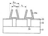
도 3a 내지 도 3h는 본 발명의 실시예에 따른 캐패시터의 제조 공정 단면도.
3A to 3H are cross-sectional views of a manufacturing process of a capacitor according to an embodiment of the present invention.
* 도면의 주요 부분에 대한 부호의 설명* Explanation of symbols for the main parts of the drawings
21 : 반도체 기판 22 : 층간절연막21
23 : 제1 식각배리어막 24 : 스토리지노드 콘택 플러그23: first etching barrier layer 24: storage node contact plug
25 : 제2 식각배리어막 26 : 제1 스토리지노드 절연막25: second etching barrier layer 26: first storage node insulating layer
27 : 필라 패턴 28 : 제2 스토리지노드 절연막27: pillar pattern 28: second storage node insulating film
29 : 오목 패턴 30a : 하부전극29
32 : 산소확산배리어막 33 : Ta2O5막32: oxygen diffusion barrier film 33: Ta2 O5 film
34 : 상부전극
34: upper electrode
본 발명은 반도체 제조 기술에 관한 것으로, 특히 캐패시터의 제조 방법에 관한 것이다.BACKGROUND OF THE INVENTION 1. Field of the Invention The present invention relates to semiconductor manufacturing techniques, and more particularly to a method of manufacturing a capacitor.
최근에 메모리 소자의 고집적화, 소형화 및 고속화에 따라 캐패시터가 차지하는 면적이 감소하고 있으며, 비록 반도체 소자가 고집적화 및 소형화되더라도 반도체 소자를 구동시키기 위한 캐패시터의 정전 용량은 최소한 확보되어야한다.In recent years, the area occupied by a capacitor has been decreasing due to the high integration, miniaturization, and high speed of the memory device. Even if the semiconductor device is highly integrated and miniaturized, the capacitance of the capacitor for driving the semiconductor device should be secured at least.
캐패시터의 정전 용량을 확보하기 위한 한 방안으로 캐패시터의 하부전극을 실린더(Cyclinder) 구조, 스택(Stack) 구조, 오목(Concave) 구조 등 다양한 구조로 형성하여 제한된 면적 하에서 캐패시터의 하부전극의 유효 표면적을 극대화시키고 있다.In order to secure the capacitance of the capacitor, the lower electrode of the capacitor is formed into various structures such as a cylinder structure, a stack structure, and a concave structure, thereby reducing the effective surface area of the capacitor's lower electrode under a limited area. Maximizing.
또한, 캐패시터 용량을 확보하기 위해 하부전극의 높이를 증가시키고 있다.In addition, the height of the lower electrode is increased to secure the capacitor capacity.
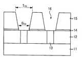
도 1a 내지 도 1d는 종래기술에 따른 캐패시터의 제조 방법을 도시한 공정 단면도이다.1A to 1D are cross-sectional views illustrating a method of manufacturing a capacitor according to the prior art.
도 1a에 도시된 바와 같이, 트랜지스터 및 비트라인 등의 반도체 회로가 형성된 반도체 기판(11) 상부에 층간절연막(12)을 형성한 후, 층간절연막(12)을 식각하여 반도체 기판(11)의 일부를 노출시키는 스토리지노드콘택홀을 형성한다.As shown in FIG. 1A, after forming the
다음에, 스토리지노드콘택홀 내에 매립되어 반도체 기판(11)과 연결되는 스토리지노드 콘택플러그(13)를 형성한 후, 스토리지노드 콘택플러그(13)를 포함한 층간절연막(12) 상에 식각배리어막(etch barrier layer)(14)과 하부전극의 높이를 결정짓는 스토리지노드 산화막(15)을 차례로 증착한다.Next, after forming the storage
다음에, 스토리지노드 산화막(15)과 식각배리어막(14)을 식각하여 하부전극이 형성될 영역, 예컨대 오목(concave) 패턴(16)을 형성한다. 이때, 오목 패턴(16)은 두꺼운 스토리지노드 산화막(15)을 건식식각하여 형성하므로 수직에 가까운 프로파일로 식각되지 않기 때문에, 상부 임계선폭(Top Critical Dimension, TCD)이 하부 임계선폭(Bottom CD, BCD)에 비해 크다. 이하, 임계선폭을 CD라고 약칭한다.Next, the storage
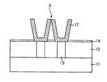
도 1b에 도시된 바와 같이, 오목패턴(16)을 포함한 전면에 하부전극용 도전막을 증착한 후, 오목 패턴(16)을 채울때까지 하부전극용 도전막 상에 감광막을 도포한다. 다음에, 에치백이나 화학적기계적연마를 통해 오목패턴(16)을 제외한 부분에 형성된 하부전극용 도전막을 제거하여 오목 패턴(16) 내부에만 잔류하는 실린더구조의 하부전극(17)을 형성한 후, 감광막을 제거한다.As shown in FIG. 1B, after the lower electrode conductive film is deposited on the entire surface including the
도 1c에 도시된 바와 같이, 스토리지노드 산화막(15)을 습식 딥아웃 공정을 통해 제거한다. 이때, 드러나는 실린더 구조의 하부전극(17)은 오목패턴(16)과 동일하게 상부 CD(TCD)가 하부 CD(BCD)에 비해 크고, 이로써 이웃한 실린더형 하부전극(17)간 간격(y1)이 좁다As illustrated in FIG. 1C, the storage
도 1d에 도시된 바와 같이, 실린더 구조의 하부전극(17) 상에 유전막(18)과 상부전극(19)를 차례로 형성하여 캐패시터를 완성한다.As shown in FIG. 1D, the
그러나, 상술한 종래기술은, 도 2에 도시된 바와 같이, 실린더 구조의 하부 전극(17)의 상부 CD(TCD)가 하부 CD(BCD)에 비해 크고, 이웃한 하부전극(17)간 간격(y1)이 좁기 때문에, 똑바로 지지되지 못하여 이웃한 하부전극(17)과 붙는 문제가 발생한다.However, in the above-described prior art, as illustrated in FIG. 2, the upper CD TCD of the
이와 같이, 하부전극(17)끼리 붙을 경우에는 듀얼 비트 페일(dual bit fail)을 유발하게 되어 각 셀을 독립적으로 동작시킬 수 없다.
As such, when the
본 발명은 상기한 종래기술의 문제점을 해결하기 위해 안출한 것으로, 하부전극의 높이가 높아지더라도 이웃한 실린더형 하부전극간 붙는 현상을 방지하는데 적합한 캐패시터의 제조 방법을 제공하는데 그 목적이 있다.
The present invention has been made to solve the above problems of the prior art, and an object of the present invention is to provide a method of manufacturing a capacitor suitable for preventing the adhesion between neighboring cylindrical lower electrodes even when the height of the lower electrode is increased.
상기 목적을 달성하기 위한 본 발명의 캐패시터의 제조 방법은 반도체 기판 상에 상기 반도체 기판의 일부를 노출시키는 홀을 갖는 층간절연막과 제1 식각배리어막의 적층막을 형성하는 단계; 상기 적층막의 홀에 매립되어 상기 반도체 기판과 연결되는 스토리지노드 콘택플러그를 형성하는 단계; 상기 적층막 상에 상기 스토리지노드 콘택플러그를 노출시키면서 하부 영역의 임계선폭이 상부 영역의 그것에 비해 큰 오목 패턴을 갖는 스토리지노드절연막을 형성하는 단계; 상기 오목 패턴 내에 상기 스토리지노드 콘택플러그와 연결되면서 하부 선폭이 상부 선폭에 비해 큰 실린더구조의 하부전극을 형성하는 단계; 상기 스토리지노드절연막을 제거하는 단계; 상기 하부전극의 표면에 산소확산배리어막을 형성하는 단계; 및 상기 산소확산배리어막이 형성된 하부전극 상에 유전막과 상부전극을 차례로 형성하는 단계를 포함하는 것을 특징으로 한다.A method of manufacturing a capacitor of the present invention for achieving the above object comprises the steps of forming a laminated film of an interlayer insulating film and a first etching barrier film having a hole for exposing a portion of the semiconductor substrate on a semiconductor substrate; Forming a storage node contact plug embedded in a hole of the stacked layer and connected to the semiconductor substrate; Forming a storage node insulating film having a concave pattern having a larger critical line width in a lower region than that in an upper region while exposing the storage node contact plug on the stacked layer; Forming a lower electrode having a cylindrical structure having a lower line width than the upper line width while being connected to the storage node contact plug in the concave pattern; Removing the storage node insulating layer; Forming an oxygen diffusion barrier film on a surface of the lower electrode; And sequentially forming a dielectric film and an upper electrode on the lower electrode on which the oxygen diffusion barrier film is formed.
또한, 본 발명의 캐패시터의 제조 방법은 반도체 기판 상에 층간절연막과 제1 식각배리어막의 적층막을 형성하는 단계; 상기 적층막을 식각하여 상기 반도체 기판의 일부를 노출시키는 스토리지노드콘택홀을 형성하는 단계; 상기 스토리지노드콘택홀에 매립되어 상기 반도체 기판과 연결되는 스토리지노드 콘택플러그를 형성하는 단계; 상기 스토리지노드 콘택플러그 및 상기 적층막 상에 제2 식각배리어막과 제1 스토리지노드절연막을 적층 형성하는 단계; 상기 제1 스토리지노드절연막과 상기 제2 식각배리어막을 순차적으로 건식식각하여 상기 스토리지노드콘택플러그 상에 하부의 임계선폭이 상부의 그것에 비해 큰 필라 패턴을 형성하는 단계; 상기 필라 패턴을 에워싸는 제2 스토리지노드절연막을 형성하는 단계; 상기 필라 패턴을 선택적으로 제거하여 상기 스토리지 노드 콘택플러그를 노출시키는 오목 패턴을 형성하는 단계; 상기 오목 패턴 내부에 상기 스토리지노드 콘택플러그와 연결되면서 하부의 임계선폭이 상부의 그것에 비해 큰 실린더 구조의 하부전극을 형성하는 단계; 상기 제2스토리지노드절연막을 제거하는 단계; 상기 하부전극의 표면을 질화시켜 산소확산배리어막을 형성하는 단계; 및 상기 산소확산배리어막이 형성된 하부전극 상에 유전막과 상부전극을 차례로 형성하는 단계를 포함하는 것을 특징으로 한다.In addition, the capacitor manufacturing method of the present invention comprises the steps of forming a laminated film of the interlayer insulating film and the first etching barrier film on the semiconductor substrate; Etching the stacked layer to form a storage node contact hole exposing a portion of the semiconductor substrate; Forming a storage node contact plug buried in the storage node contact hole and connected to the semiconductor substrate; Stacking a second etching barrier layer and a first storage node insulating layer on the storage node contact plug and the lamination layer; Sequentially etching the first storage node insulating layer and the second etching barrier layer to form a pillar pattern on the storage node contact plug having a lower critical line width than that of an upper portion thereof; Forming a second storage node insulating layer surrounding the pillar pattern; Selectively removing the pillar pattern to form a concave pattern exposing the storage node contact plug; Forming a lower electrode of a cylindrical structure having a lower critical line width than that of the upper part while being connected to the storage node contact plug in the concave pattern; Removing the second storage node insulating layer; Nitriding the surface of the lower electrode to form an oxygen diffusion barrier film; And sequentially forming a dielectric film and an upper electrode on the lower electrode on which the oxygen diffusion barrier film is formed.
이하, 본 발명이 속하는 기술분야에서 통상의 지식을 가진 자가 본 발명의 기술적 사상을 용이하게 실시할 수 있을 정도로 상세히 설명하기 위하여, 본 발명의 가장 바람직한 실시예를 첨부 도면을 참조하여 설명하기로 한다.Hereinafter, the preferred embodiments of the present invention will be described in detail with reference to the accompanying drawings so that those skilled in the art may easily implement the technical idea of the present invention. .
도 3a 내지 도 3h는 본 발명의 실시예에 따른 캐패시터의 제조 방법을 도시 한 공정 단면도이다.3A to 3H are cross-sectional views illustrating a method of manufacturing a capacitor according to an embodiment of the present invention.
도 3a에 도시된 바와 같이, 트랜지스터 및 비트라인 등의 반도체 회로가 형성된 반도체 기판(21) 상부에 층간절연막(22)과 제1 식각배리어막(23)을 증착한다. 이때, 제1 식각배리어막(23)은 300Å∼1000Å의 두께로 증착한 질화막(nitride)이며, 후속 건식식각 배리어막 역할 및 제1 스토리지노드 절연막의 습식식각 배리어막 역할을 한다.As shown in FIG. 3A, an
다음에, 마스크 및 식각 공정을 통해 제1 식각배리어막(23)과 층간절연막(22)을 식각하여 반도체 기판(21)의 일부분을 노출시키는 스토리지노드콘택홀을 형성한 후, 스토리지노드콘택홀을 채울때까지 제1 식각배리어막(23) 상에 폴리실리콘막을 증착한다.Next, the first
그리고, 제1 식각배리어막(23)의 표면이 드러날때까지 폴리실리콘막을 화학적기계적연마(CMP) 공정으로 평탄화시켜 폴리실리콘막으로 된 스토리지노드 콘택플러그(24)를 형성한다.Then, the polysilicon film is planarized by a chemical mechanical polishing (CMP) process until the surface of the first
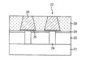
도 3b에 도시된 바와 같이, 스토리지노드 콘택플러그(24) 및 제1 식각배리어막(23) 상에 폴리실리콘막(polysilicon) 또는 티타늄나이트라이드막(TiN)으로 된 제2 식각배리어막(25)을 300Å∼1000Å의 두께로 형성하고, 제2 식각배리어막(25) 상에 질화막(Si3N4)의 제1 스토리지노드 절연막(26)을 5000Å∼30000Å의 두께로 형성한다.As shown in FIG. 3B, a second
이때, 제2 식각배리어막(25)은 제1 스토리지노드 절연막(26)의 건식식각 배 리어막 역할과 이후 진행되는 제1 스토리지노드 절연막(26)의 습식식각 배리어막 역할을 한다.In this case, the second
다음에, 마스크 및 식각 공정을 통해 제2 식각배리어막(25)에서 식각이 멈추도록 제1 스토리지노드절연막(26)을 건식식각하고, 연속해서 제1 식각배리어막(23)에서 식각이 멈추도록 제2 식각배리어막(25)을 건식식각하여 스토리지노드 콘택플러그(24)에 접하며 상부 CD(TCD)에 비해 하부 CD(BCD)가 넓은 필라(pillar) 패턴(27)을 형성한다.Next, the first storage
도 3c에 도시된 바와 같이, 필라 패턴(27)간 공간을 채울때까지 필라 패턴(27) 상에 제2 스토리지노드 절연막(28)을 형성한 후, 필라 패턴(27)의 제1 스토리지노드 절연막(26)의 표면이 드러날때까지 제2 스토리지노드 절연막(28)을 화학적기계적연마하여 평탄화한다.As shown in FIG. 3C, after forming the second storage
여기서, 제2 스토리지노드 절연막(28)은 USG(Undoped Silicate Glass), PSG(Phospho Silicate Glass), BPSG(Boro Phospho Silicate Glass) 또는 PETEOS(Plasma Enhance Tetra Ethyl Ortho Silicate) 중에서 선택하여 사용한다.Here, the second storage
도 3d에 도시된 바와 같이, 필라 패턴(27)을 선택적으로 제거하는데, 먼저 H3PO4 용액을 이용하여 제1 스토리지노드 절연막(26)을 습식식각하고, 건식식각을 통해 제2 식각배리어막(25)을 식각한다.As shown in FIG. 3D, the
이때, 제2 식각배리어막(25)은 제1 스토리지노드 절연막(26)의 습식식각시 식각배리어막이고, 제1 식각배리어막(23)은 제2 식각배리어막(25)의 건식 식각시 식각배리어막이다.In this case, the second
한편, 제2 식각배리어막(25)은 건식식각외에 습식식각을 통해서도 제거할 수 있는데, 제2 식각배리어막(25)이 폴리실리콘막인 경우에는 HNO3/HF/CH3COOH의 혼합 수용액을 이용하여 습식식각하고, 제2 식각배리어막(25)이 티타늄나이트라이드막인 경우에는 H2SO4/H2O2의 혼합수용액을 이용하여 습식식각한다.On the other hand, the second
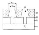
전술한 바와 같은 필라 패턴(27)의 제거후, 제2 스토리지노드 절연막(28)이 제공하는 오목 패턴(29)이 형성되며, 오목 패턴(29)은 필라 패턴(27)과 동일하게 상부 CD(TCD)가 하부 CD(BCD)에 비해 작으며, 스토리지노드 콘택플러그(24)를 노출시키는 스토리지노드 예정 영역이다.After removing the
도 3e에 도시된 바와 같이, 오목 패턴(29)을 포함한 제2 스토리지노드 절연막(28) 상에 하부전극용 도전막(30)을 증착한 후, 하부전극용 도전막(30) 상에 오목 패턴(29)을 채우는 두께로 감광막(31)을 도포한다. 이때, 하부전극용 도전막(30)은 도우프드 폴리실리콘막 또는 귀금속(noble metal) 계열의 금속막을 이용한다.As shown in FIG. 3E, after the lower electrode
도 3f에 도시된 바와 같이, 하부전극용 도전막(30)의 에치백 또는 화학적기계적연마 공정을 통해 오목 패턴(29) 내에만 잔류하는 실린더 구조의 하부전극(30a)을 형성한다.As illustrated in FIG. 3F, a cylindrical
자세히 살펴 보면, 하부전극용 도전막(30) 표면이 드러날때까지 감광막(31)을 에치백하여 오목 패턴(29) 내부에 감광막(31)을 잔류시키고, 감광막(31)이 잔류 한 상태에서 오목 패턴(29) 외부의 제2 스토리지노드 절연막(28)상에 드러난 하부전극용 도전막(30)을 에치백 또는 화학적기계적연마하여 실린더 구조의 하부전극(30a)을 형성한다.In detail, the
도 3g에 도시된 바와 같이, 잔류하는 감광막(31)을 스트립하여 제거한 후, HF 또는 BOE(Buffered Oxide Etchant)를 이용하여 제2 스토리지노드 절연막(28)을 습식식각한다. 이때, 실린더 구조의 하부전극(30a)의 외벽이 드러난다.As shown in FIG. 3G, after the remaining
전술한 바에 따르면, 실린더 구조의 하부전극(30a)은 오목패턴(29)의 내부에 형성됨에 따라 하부 CD(BCD)가 상부 CD(TCD)에 비해 크고, 이로써 실린더 구조의 하부전극(30a)이 견고하게 지지되고, 이웃한 실린더 구조의 하부전극(30a)의 상부 간격(y2)이 넓다.According to the foregoing, the lower electrode (30a) of the cylinder structure is greater than the lower CD (BCD) the upper CD (TCD) depending on the formed in the interior of the
도 3h에 도시된 바와 같이, 실린더 구조의 하부전극(30a) 표면을 NH3 플라즈마처리하여 질화시켜 후속 유전막의 열처리시 산소가 실린더 구조의 하부전극(30a)으로 확산하는 것을 방지하는 산소확산배리어막(32)을 형성한다.As shown in FIG. 3H, the surface of the
이때, 질화시키는 공정은, 300℃∼ 500℃의 온도와 0.1torr∼10torr의 압력하에서 100W∼1000W의 RF 파워를 인가하면서 진행한다.At this time, the step of nitriding proceeds while applying an RF power of 100 W to 1000 W at a temperature of 300 ° C. to 500 ° C. and a pressure of 0.1 tor to 10 tor.
다음에, 질화된 실린더 구조의 하부전극(30a) 상에 Ta2O5막(33)을 20Å∼100Å의 두께로 증착한다. 이때, Ta2O5막(33)의 증착은 300℃∼ 500℃의 온도와 0.1torr∼1torr의 압력에서 Ta(C2H5O)5 소스와 반응가스인 산소(O2)를 이용하여 진행 한다.Next, a Ta2 O5 film 33 is deposited to a thickness of 20 kPa to 100 kPa on the
다음에, Ta2O5막(33)의 특성 향상 및 결정화를 위해 500℃∼800℃의 고온에서 N2O 또는 O2 분위기로 로(furnace)를 이용하여 열처리한다.Next, in order to improve the characteristics and crystallization of the Ta2 O5 film 33, heat treatment is performed using a furnace in an N2 O or O2 atmosphere at a high temperature of 500 ° C. to 800 ° C.
마지막으로, 상부전극(34)을 증착한 후, 패터닝을 통해 캐패시터를 완성한다. 이때, 상부전극(34)의 물질로는 CVD TiN을 증착한 후 폴리실리콘막을 연속해서 증착한다. 그리고 500℃∼700℃의 온도로 질소 분위기에서 로를 이용하여 활성화 열처리를 실시한다.Finally, after depositing the
본 발명의 기술 사상은 상기 바람직한 실시예에 따라 구체적으로 기술되었으나, 상기한 실시예는 그 설명을 위한 것이며 그 제한을 위한 것이 아님을 주의하여야 한다. 또한, 본 발명의 기술 분야의 통상의 전문가라면 본 발명의 기술 사상의 범위 내에서 다양한 실시예가 가능함을 이해할 수 있을 것이다.
Although the technical idea of the present invention has been described in detail according to the above preferred embodiment, it should be noted that the above-described embodiment is for the purpose of description and not of limitation. In addition, those skilled in the art will understand that various embodiments are possible within the scope of the technical idea of the present invention.
상술한 본 발명은 실린더 구조의 하부전극의 하부 CD(BCD)가 상부 CD(TCD)에 비해 크므로, 하부전극이 견고하게 지지되고, 또한 이웃한 실린더 구조의 하부전극간 상부 간격이 넓어 실린더 구조의 하부전극들이 서로 붙는 현상을 억제하므로 셀 사이의 듀얼 비트 페일을 방지하여 웨이퍼의 수율을 향상시킬 수 있는 효과가 있다.In the present invention described above, since the lower CD (BCD ) of the lower electrode of the cylinder structure is larger than the upper CD (TCD ), the lower electrode is firmly supported, and the upper interval between the lower electrodes of the adjacent cylinder structure is wider. Since the lower electrodes of the cylinder structure are prevented from adhering to each other, dual bit failing between cells can be prevented, thereby improving wafer yield.
Claims (18)
Translated fromKoreanPriority Applications (2)
| Application Number | Priority Date | Filing Date | Title |
|---|---|---|---|
| KR1020020086394AKR100721579B1 (en) | 2002-12-30 | 2002-12-30 | Manufacturing method of capacitor |
| US10/615,087US6960504B2 (en) | 2002-12-30 | 2003-07-09 | Method for fabricating capacitor |
Applications Claiming Priority (1)
| Application Number | Priority Date | Filing Date | Title |
|---|---|---|---|
| KR1020020086394AKR100721579B1 (en) | 2002-12-30 | 2002-12-30 | Manufacturing method of capacitor |
Publications (2)
| Publication Number | Publication Date |
|---|---|
| KR20040059889A KR20040059889A (en) | 2004-07-06 |
| KR100721579B1true KR100721579B1 (en) | 2007-05-23 |
Family
ID=32653212
Family Applications (1)
| Application Number | Title | Priority Date | Filing Date |
|---|---|---|---|
| KR1020020086394AExpired - Fee RelatedKR100721579B1 (en) | 2002-12-30 | 2002-12-30 | Manufacturing method of capacitor |
Country Status (2)
| Country | Link |
|---|---|
| US (1) | US6960504B2 (en) |
| KR (1) | KR100721579B1 (en) |
Families Citing this family (9)
| Publication number | Priority date | Publication date | Assignee | Title |
|---|---|---|---|---|
| KR100721579B1 (en)* | 2002-12-30 | 2007-05-23 | 주식회사 하이닉스반도체 | Manufacturing method of capacitor |
| KR100668833B1 (en)* | 2004-12-17 | 2007-01-16 | 주식회사 하이닉스반도체 | Capacitor Manufacturing Method of Semiconductor Device |
| US8008701B2 (en)* | 2004-12-22 | 2011-08-30 | Giorgio Servalli | Method of making a floating gate non-volatile MOS semiconductor memory device with improved capacitive coupling and device thus obtained |
| EP2018660B1 (en)* | 2006-05-02 | 2020-03-25 | Murata Integrated Passive Solutions | Electric device comprising an electrode with enhanced stability |
| US8040721B2 (en)* | 2009-08-31 | 2011-10-18 | Sandisk 3D Llc | Creating short program pulses in asymmetric memory arrays |
| KR101883380B1 (en)* | 2011-12-26 | 2018-07-31 | 삼성전자주식회사 | Semiconductor device having capacitors |
| US10643936B2 (en)* | 2017-05-31 | 2020-05-05 | Dyi-chung Hu | Package substrate and package structure |
| CN114284268A (en)* | 2020-09-27 | 2022-04-05 | 中国科学院微电子研究所 | Capacitor, method for making the same, and electronic device |
| CN114334977A (en)* | 2020-10-10 | 2022-04-12 | 中国科学院微电子研究所 | Semiconductor device and manufacturing method thereof |
Citations (3)
| Publication number | Priority date | Publication date | Assignee | Title |
|---|---|---|---|---|
| KR20000002832A (en)* | 1998-06-23 | 2000-01-15 | 윤종용 | Production method of semiconductor device and capacitor formed thereby |
| KR20000040534A (en)* | 1998-12-18 | 2000-07-05 | 윤종용 | Method for manufacturing capacitor of semiconductor device by using an electric plating |
| KR20020084595A (en)* | 2001-05-03 | 2002-11-09 | 주식회사 하이닉스반도체 | Method for fabricating capacitor |
Family Cites Families (12)
| Publication number | Priority date | Publication date | Assignee | Title |
|---|---|---|---|---|
| US5754390A (en)* | 1996-01-23 | 1998-05-19 | Micron Technology, Inc. | Integrated capacitor bottom electrode for use with conformal dielectric |
| US6911371B2 (en)* | 1997-12-19 | 2005-06-28 | Micron Technology, Inc. | Capacitor forming methods with barrier layers to threshold voltage shift inducing material |
| US6496352B2 (en)* | 1998-06-30 | 2002-12-17 | Texas Instruments Incorporated | Post-in-crown capacitor and method of manufacture |
| US6284551B1 (en)* | 1999-06-14 | 2001-09-04 | Hyundai Electronics Industries Co., Ltd. | Capacitor and method for fabricating the same |
| US6429087B2 (en)* | 1999-08-30 | 2002-08-06 | Micron Technology, Inc. | Methods of forming capacitors |
| US6611017B2 (en)* | 2000-03-27 | 2003-08-26 | Kabushiki Kaisha Toshiba | Semiconductor device provided with capacitor having cavity-provided electrode |
| US20020168847A1 (en)* | 2001-05-09 | 2002-11-14 | Applied Materials, Inc. | Methods of forming a nitridated surface on a metallic layer and products produced thereby |
| US6825081B2 (en)* | 2001-07-24 | 2004-11-30 | Micron Technology, Inc. | Cell nitride nucleation on insulative layers and reduced corner leakage of container capacitors |
| KR100500940B1 (en)* | 2002-06-21 | 2005-07-14 | 주식회사 하이닉스반도체 | Method for fabricating capacitor in semiconductor device |
| US6664198B1 (en)* | 2002-07-03 | 2003-12-16 | Micron Technology, Inc. | Method of forming a silicon nitride dielectric layer |
| KR100721579B1 (en)* | 2002-12-30 | 2007-05-23 | 주식회사 하이닉스반도체 | Manufacturing method of capacitor |
| TWI271872B (en)* | 2002-12-30 | 2007-01-21 | Hynix Semiconductor Inc | Capacitor and method for fabricating the same |
- 2002
- 2002-12-30KRKR1020020086394Apatent/KR100721579B1/ennot_activeExpired - Fee Related
- 2003
- 2003-07-09USUS10/615,087patent/US6960504B2/ennot_activeExpired - Fee Related
Patent Citations (3)
| Publication number | Priority date | Publication date | Assignee | Title |
|---|---|---|---|---|
| KR20000002832A (en)* | 1998-06-23 | 2000-01-15 | 윤종용 | Production method of semiconductor device and capacitor formed thereby |
| KR20000040534A (en)* | 1998-12-18 | 2000-07-05 | 윤종용 | Method for manufacturing capacitor of semiconductor device by using an electric plating |
| KR20020084595A (en)* | 2001-05-03 | 2002-11-09 | 주식회사 하이닉스반도체 | Method for fabricating capacitor |
Also Published As
| Publication number | Publication date |
|---|---|
| US6960504B2 (en) | 2005-11-01 |
| KR20040059889A (en) | 2004-07-06 |
| US20040126982A1 (en) | 2004-07-01 |
Similar Documents
| Publication | Publication Date | Title |
|---|---|---|
| KR100553839B1 (en) | Capacitor and manufacturing method thereof, semiconductor device comprising same and manufacturing method thereof | |
| KR100459724B1 (en) | Semiconductor device having a SiN etch stopper by low temperature ALD and fabricating method the same | |
| KR100655774B1 (en) | Etch stop structure, manufacturing method thereof, semiconductor device comprising same and manufacturing method thereof | |
| KR100721579B1 (en) | Manufacturing method of capacitor | |
| KR100366634B1 (en) | Method for manufacturing semiconductor device | |
| KR100238615B1 (en) | Method of manufacturing a semiconductor memory device with a stacked capacitor | |
| US6924189B2 (en) | Method for manufacturing capacitor bottom electrode of semiconductor device | |
| KR100721546B1 (en) | Capacitor and Method of Manufacturing the Same | |
| KR100300046B1 (en) | Fabricating method of semiconductor device | |
| KR100465836B1 (en) | Method for fabricating capacitor | |
| KR100388453B1 (en) | Method for fabricating capacitor | |
| JP2002009259A (en) | Semiconductor device and manufacturing method thereof | |
| KR20030000695A (en) | Method for forming the storage node of semiconductor device | |
| KR20050011944A (en) | Fabricating method of semiconductor device | |
| KR20040008626A (en) | Method for fabricating cylinder type capacitor | |
| JP2011054676A (en) | Method of manufacturing semiconductor device | |
| KR100253326B1 (en) | Method for semiconductor device | |
| KR20040039592A (en) | Method of manufacturing a capacitor of a semiconductor device | |
| KR20050067476A (en) | Method for manufacturing capacitor | |
| KR20020024738A (en) | Method for manufacturing storage node electrode of semiconductor memory device | |
| KR20060000964A (en) | Manufacturing Method of Semiconductor Device | |
| KR20010003745A (en) | Method of manufacturing semiconductor memory device | |
| KR20090122560A (en) | Capacitor and manufacturing method thereof | |
| KR20040057583A (en) | Method of forming contact hole in semiconductor device | |
| KR20060117805A (en) | Cylindrical capacitor lower electrode film formation method of semiconductor device |
Legal Events
| Date | Code | Title | Description |
|---|---|---|---|
| PA0109 | Patent application | St.27 status event code:A-0-1-A10-A12-nap-PA0109 | |
| PG1501 | Laying open of application | St.27 status event code:A-1-1-Q10-Q12-nap-PG1501 | |
| A201 | Request for examination | ||
| PA0201 | Request for examination | St.27 status event code:A-1-2-D10-D11-exm-PA0201 | |
| D13-X000 | Search requested | St.27 status event code:A-1-2-D10-D13-srh-X000 | |
| D14-X000 | Search report completed | St.27 status event code:A-1-2-D10-D14-srh-X000 | |
| E902 | Notification of reason for refusal | ||
| PE0902 | Notice of grounds for rejection | St.27 status event code:A-1-2-D10-D21-exm-PE0902 | |
| T11-X000 | Administrative time limit extension requested | St.27 status event code:U-3-3-T10-T11-oth-X000 | |
| P11-X000 | Amendment of application requested | St.27 status event code:A-2-2-P10-P11-nap-X000 | |
| P13-X000 | Application amended | St.27 status event code:A-2-2-P10-P13-nap-X000 | |
| E701 | Decision to grant or registration of patent right | ||
| PE0701 | Decision of registration | St.27 status event code:A-1-2-D10-D22-exm-PE0701 | |
| GRNT | Written decision to grant | ||
| PR0701 | Registration of establishment | St.27 status event code:A-2-4-F10-F11-exm-PR0701 | |
| PR1002 | Payment of registration fee | St.27 status event code:A-2-2-U10-U11-oth-PR1002 Fee payment year number:1 | |
| PG1601 | Publication of registration | St.27 status event code:A-4-4-Q10-Q13-nap-PG1601 | |
| PR1001 | Payment of annual fee | St.27 status event code:A-4-4-U10-U11-oth-PR1001 Fee payment year number:4 | |
| PR1001 | Payment of annual fee | St.27 status event code:A-4-4-U10-U11-oth-PR1001 Fee payment year number:5 | |
| PN2301 | Change of applicant | St.27 status event code:A-5-5-R10-R13-asn-PN2301 St.27 status event code:A-5-5-R10-R11-asn-PN2301 | |
| FPAY | Annual fee payment | Payment date:20120424 Year of fee payment:6 | |
| PR1001 | Payment of annual fee | St.27 status event code:A-4-4-U10-U11-oth-PR1001 Fee payment year number:6 | |
| PN2301 | Change of applicant | St.27 status event code:A-5-5-R10-R13-asn-PN2301 St.27 status event code:A-5-5-R10-R11-asn-PN2301 | |
| LAPS | Lapse due to unpaid annual fee | ||
| PC1903 | Unpaid annual fee | St.27 status event code:A-4-4-U10-U13-oth-PC1903 Not in force date:20130518 Payment event data comment text:Termination Category : DEFAULT_OF_REGISTRATION_FEE | |
| PC1903 | Unpaid annual fee | St.27 status event code:N-4-6-H10-H13-oth-PC1903 Ip right cessation event data comment text:Termination Category : DEFAULT_OF_REGISTRATION_FEE Not in force date:20130518 | |
| PN2301 | Change of applicant | St.27 status event code:A-5-5-R10-R13-asn-PN2301 St.27 status event code:A-5-5-R10-R11-asn-PN2301 | |
| P22-X000 | Classification modified | St.27 status event code:A-4-4-P10-P22-nap-X000 |