KR100720988B1 - Plasma processing chamber with embedded induction antenna - Google Patents
Plasma processing chamber with embedded induction antennaDownload PDFInfo
- Publication number
- KR100720988B1 KR100720988B1KR1020060022502AKR20060022502AKR100720988B1KR 100720988 B1KR100720988 B1KR 100720988B1KR 1020060022502 AKR1020060022502 AKR 1020060022502AKR 20060022502 AKR20060022502 AKR 20060022502AKR 100720988 B1KR100720988 B1KR 100720988B1
- Authority
- KR
- South Korea
- Prior art keywords
- plasma processing
- processing chamber
- chamber
- induction antenna
- induction
- Prior art date
- Legal status (The legal status is an assumption and is not a legal conclusion. Google has not performed a legal analysis and makes no representation as to the accuracy of the status listed.)
- Expired - Fee Related
Links
Images


Classifications
- H—ELECTRICITY
- H01—ELECTRIC ELEMENTS
- H01L—SEMICONDUCTOR DEVICES NOT COVERED BY CLASS H10
- H01L21/00—Processes or apparatus adapted for the manufacture or treatment of semiconductor or solid state devices or of parts thereof
- H01L21/67—Apparatus specially adapted for handling semiconductor or electric solid state devices during manufacture or treatment thereof; Apparatus specially adapted for handling wafers during manufacture or treatment of semiconductor or electric solid state devices or components ; Apparatus not specifically provided for elsewhere
- H01L21/67005—Apparatus not specifically provided for elsewhere
- H01L21/67011—Apparatus for manufacture or treatment
- H01L21/67017—Apparatus for fluid treatment
- H01L21/67063—Apparatus for fluid treatment for etching
- H01L21/67069—Apparatus for fluid treatment for etching for drying etching
- H—ELECTRICITY
- H01—ELECTRIC ELEMENTS
- H01L—SEMICONDUCTOR DEVICES NOT COVERED BY CLASS H10
- H01L21/00—Processes or apparatus adapted for the manufacture or treatment of semiconductor or solid state devices or of parts thereof
- H01L21/02—Manufacture or treatment of semiconductor devices or of parts thereof
- H01L21/02041—Cleaning
- H01L21/205—
- H—ELECTRICITY
- H01—ELECTRIC ELEMENTS
- H01L—SEMICONDUCTOR DEVICES NOT COVERED BY CLASS H10
- H01L21/00—Processes or apparatus adapted for the manufacture or treatment of semiconductor or solid state devices or of parts thereof
- H01L21/02—Manufacture or treatment of semiconductor devices or of parts thereof
- H01L21/04—Manufacture or treatment of semiconductor devices or of parts thereof the devices having potential barriers, e.g. a PN junction, depletion layer or carrier concentration layer
- H01L21/18—Manufacture or treatment of semiconductor devices or of parts thereof the devices having potential barriers, e.g. a PN junction, depletion layer or carrier concentration layer the devices having semiconductor bodies comprising elements of Group IV of the Periodic Table or AIIIBV compounds with or without impurities, e.g. doping materials
- H01L21/30—Treatment of semiconductor bodies using processes or apparatus not provided for in groups H01L21/20 - H01L21/26
- H01L21/302—Treatment of semiconductor bodies using processes or apparatus not provided for in groups H01L21/20 - H01L21/26 to change their surface-physical characteristics or shape, e.g. etching, polishing, cutting
- H01L21/306—Chemical or electrical treatment, e.g. electrolytic etching
- H01L21/3065—Plasma etching; Reactive-ion etching
- H—ELECTRICITY
- H01—ELECTRIC ELEMENTS
- H01L—SEMICONDUCTOR DEVICES NOT COVERED BY CLASS H10
- H01L21/00—Processes or apparatus adapted for the manufacture or treatment of semiconductor or solid state devices or of parts thereof
- H01L21/67—Apparatus specially adapted for handling semiconductor or electric solid state devices during manufacture or treatment thereof; Apparatus specially adapted for handling wafers during manufacture or treatment of semiconductor or electric solid state devices or components ; Apparatus not specifically provided for elsewhere
- H01L21/67005—Apparatus not specifically provided for elsewhere
- H01L21/67011—Apparatus for manufacture or treatment
- H01L21/67155—Apparatus for manufacturing or treating in a plurality of work-stations
- H01L21/67207—Apparatus for manufacturing or treating in a plurality of work-stations comprising a chamber adapted to a particular process
Landscapes
- Engineering & Computer Science (AREA)
- Physics & Mathematics (AREA)
- Condensed Matter Physics & Semiconductors (AREA)
- General Physics & Mathematics (AREA)
- Manufacturing & Machinery (AREA)
- Computer Hardware Design (AREA)
- Microelectronics & Electronic Packaging (AREA)
- Power Engineering (AREA)
- Plasma & Fusion (AREA)
- Chemical Vapour Deposition (AREA)
- Plasma Technology (AREA)
Abstract
Translated fromKoreanDescription
Translated fromKorean본 발명의 상세한 설명에서 사용되는 도면을 보다 충분히 이해하기 위하여, 각 도면의 간단한 설명이 제공된다.In order to more fully understand the drawings used in the detailed description of the invention, a brief description of each drawing is provided.
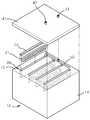
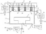
도 1은 본 발명의 바람직한 실시예에 따른 플라즈마 처리 챔버를 개략적으로 보여주는 사시도이다.1 is a perspective view schematically showing a plasma processing chamber according to a preferred embodiment of the present invention.
도 2는 도 1의 플라즈마 처리 챔버의 단면도이다.2 is a cross-sectional view of the plasma processing chamber of FIG. 1.
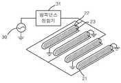
도 3 내지 도 5는 유도 안테나의 전기적 연결 구조의 다양한 실시예를 보여주는 도면이다.3 to 5 illustrate various embodiments of an electrical connection structure of an induction antenna.
도 6은 두 개의 유도 안테나가 매설된 플라즈마 처리 챔버를 개략적으로 보여주는 사시도이다.6 is a perspective view schematically showing a plasma processing chamber in which two induction antennas are embedded.
도 7은 도 6의 플라즈마 처리 챔버의 단면도이다.7 is a cross-sectional view of the plasma processing chamber of FIG. 6.
도 8은 단일 유도 안테나가 매설된 플라즈마 처리 챔버의 개략적인 사시도이다.8 is a schematic perspective view of a plasma processing chamber in which a single induction antenna is embedded.
도 9는 도 8의 플라즈마 처리 챔버의 단면도이다.9 is a cross-sectional view of the plasma processing chamber of FIG. 8.
도 10은 이중 바이어스 구조의 플라즈마 처리 챔버를 보여주는 도면이다.10 illustrates a plasma processing chamber of a dual bias structure.
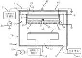
도 11은 유도 안테나의 전원 공급원을 이용하여 안테나 매설부의 전극과 챔 버 상부로 고주파 전원이 공급되도록 변형한 예를 보여주는 도면이다.FIG. 11 is a diagram illustrating an example in which high frequency power is supplied to an electrode of an antenna embedded part and an upper portion of a chamber by using a power supply source of an induction antenna.
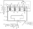
도 12는 별도의 전원 공급원을 이용하여 안테나 매설부의 전극과 챔버 상부로 고주파 전원이 공급되도록 변형한 예를 보여주는 도면이다.FIG. 12 is a diagram illustrating an example in which a high frequency power is supplied to an electrode of an antenna embedded part and an upper portion of a chamber by using a separate power supply source.
*도면의 주요 부분에 대한 부호의 설명** Description of the symbols for the main parts of the drawings *
10: 플라즈마 처리 챔버11: 피처리 기판10: plasma processing chamber 11: substrate to be processed
12: 서셉터13: 중공 영역12: susceptor 13: hollow area
14: 챔버 하우징15: 챔버 상부14: chamber housing 15: chamber top
17: 진공펌프18: 절연부재17: vacuum pump 18: insulating member
20: 유도 안테나 매설부21; 유도 안테나20: induction antenna buried
본 발명은 반도체 기판 처리를 위한 플라즈마 소오스에 관한 것으로, 구체적으로는 플라즈마 처리 챔버의 상부에 매설되는 유도 안테나를 갖는 유도 결합 플라즈마(Inductive Coupled Plasma) 소오스를 갖는 플라즈마 처리 챔버에 관한 것이다.The present invention relates to a plasma source for processing a semiconductor substrate, and more particularly, to a plasma processing chamber having an inductive coupled plasma source having an induction antenna embedded in an upper portion of the plasma processing chamber.
반도체 소자의 초미세화와 기판 사이즈의 증가 그리고 새로운 처리 대상 물질 등장 등의 여러 요인으로 인하여 반도체 제조 공정에서는 더욱 향상된 기판 처리 기술이 요구되고 있다. 특히, 플라즈마를 이용한 반도체 제조 공정으로 건식 에칭 공정 분야나 물리적/화학적 기상 증착 분야에서는 이러한 요구는 더욱 그러하 다.Due to various factors such as ultra miniaturization of semiconductor devices, an increase in substrate size, and the emergence of new materials to be treated, further improvements in substrate processing technologies are required in the semiconductor manufacturing process. This is especially true in the field of dry etching processes and physical / chemical vapor deposition as plasma semiconductor manufacturing processes.
이러한 요구에 대응하는 대표적인 기술의 하나가 유도 결합 플라즈마 기술이다. 유도 결합 플라즈마는 플라즈마 처리 챔버의 외부의 안테나에 고주파(Radio Frequency)를 인가하여 플라즈마 처리 챔버의 내부에 저압, 고밀도의 플라즈마를 발생한다. 이러한 유도 결합 플라즈마는 안테나에 인가되는 고주파 전원과 기판이 놓이는 서셉터에 바이어스를 인가하는 별도의 고주파 전원이 분리되어 있다. 그럼으로 분리된 고주파 전원을 이용하여 이온의 밀도와 이온의 가속전압을 조절할 수 있다.One representative technology that addresses this need is inductively coupled plasma technology. Inductively coupled plasma generates a low pressure, high density plasma in the plasma processing chamber by applying a radio frequency to an antenna outside the plasma processing chamber. The inductively coupled plasma is separated from a high frequency power source applied to an antenna and a separate high frequency power source applying a bias to a susceptor on which a substrate is placed. Therefore, the separated high frequency power source can be used to control ion density and ion acceleration voltage.
기판 사이즈의 증가에 따라 기판이 처리되는 플라즈마 처리 챔버의 사이즈도 증가되는데 이러한 경우 플라즈마 처리 챔버의 내부에 균일한 플라즈마를 얻기가 어렵다. 특히, 평판 나선형의 유도 결합 플라즈마 소오스의 경우에는 평판 나선형 안테나의 구조적 특징에 의해 안테나의 중심 부분에 플라즈마 밀도가 높은 문제점이 있다. 이와 같은 플라즈마 밀도의 불균형의 문제점은 대면적의 기판을 균일하게 처리하기 어렵게 만든다.As the substrate size increases, the size of the plasma processing chamber in which the substrate is processed also increases. In this case, it is difficult to obtain a uniform plasma inside the plasma processing chamber. In particular, in the case of a flat spiral inductively coupled plasma source, there is a problem in that the plasma density is high in the central portion of the antenna due to the structural characteristics of the flat spiral antenna. This problem of plasma density imbalance makes it difficult to uniformly treat a large area of substrate.
한편, 플라즈마 처리 챔버는 기판 처리시 오염되는 챔버 내부를 주기적으로 세정해야 한다. 챔버 세정에서는 보통 C3F8, NF3, SF6등과 같은 불소(fluorine) 계열의 가스가 사용되며 현재에는 주로 NF3 가스가 사용되고 있다. NF3 가스는 플라즈마 반응에 의해 활성 불소가 만들어지며, 이에 의해서 플라즈마 처리 챔버의 내부 표면에 부착된 오염막과 반응하여 휘발성 반응물의 형태로 배출된다.On the other hand, the plasma processing chamber should periodically clean the inside of the chamber contaminated during substrate processing. In chamber cleaning, fluorine-based gases such as C3 F8 , NF3 , SF6, etc. are commonly used. Currently, NF3 gas is mainly used. The NF3 gas generates active fluorine by a plasma reaction, whereby it reacts with a fouling film attached to the inner surface of the plasma processing chamber and is discharged in the form of volatile reactants.
그런데 챔버 세정시 활성 불소가 재결합, 미반응 활성 불소의 배출, 챔버 크리닝의 비균일성 등에 의해 챔버 세정이 전체적으로 고르게 이루어지기 위해서는 상당 시간이 소요되어 생산성을 낮추는 문제점으로 지적되고 있다.However, it is pointed out that it takes a long time for the chamber cleaning to be uniformly performed by the recombination of active fluorine during the chamber cleaning, the discharge of unreacted active fluorine, and the nonuniformity of the chamber cleaning, thereby lowering the productivity.
따라서 본 발명은 플라즈마 처리 챔버 내부에 고밀도의 플라즈마를 보다 균일하게 형성할 수 있도록 하나 이상의 유도 안테나가 챔버 상부에 매설된 유도 결합 플라즈마 방식의 플라즈마 처리 챔버를 제공하는데 그 목적이 있다.Accordingly, an object of the present invention is to provide an inductively coupled plasma type plasma processing chamber in which one or more induction antennas are embedded in the upper portion of the chamber so as to more uniformly form a high density plasma in the plasma processing chamber.
본 발명의 다른 목적은 플라즈마 처리 챔버 내부에 고밀도의 플라즈마를 보다 균일하게 형성할 수 있도록 하나 이상의 유도 안테나가 챔버 상부에 매설되며, 이러한 플라즈마 처리 챔버의 세정 효율을 높일 수 있는 챔버 세정 방식을 갖는 플라즈마 처리 챔버를 제공하는데 있다.Another object of the present invention is one or more induction antennas are embedded in the upper portion of the chamber to more uniformly form a high-density plasma in the plasma processing chamber, the plasma having a chamber cleaning method to increase the cleaning efficiency of the plasma processing chamber It is to provide a processing chamber.
본 발명의 또 다른 다른 목적은 플라즈마 처리 챔버 내부에 고밀도의 플라즈마를 보다 균일하게 형성할 수 있도록 하나 이상의 유도 안테나가 챔버 상부에 매설되며, 이러한 플라즈마 처리 챔버의 플라즈마 처리 효율을 높이기 위하여 분리된 가스 공급 구조를 갖는 플라즈마 처리 챔버를 제공하는데 있다.Another object of the present invention is one or more induction antennas are embedded in the upper portion of the chamber to more uniformly form a high-density plasma in the plasma processing chamber, the separated gas supply to increase the plasma processing efficiency of the plasma processing chamber It is to provide a plasma processing chamber having a structure.
상기한 기술적 과제를 달성하기 위한 본 발명의 일면은 플라즈마 처리 챔버에 관한 것이다. 본 발명의 플라즈마 처리 챔버는: 피처리 기판이 놓이는 서셉터가 내부에 구비되고 서셉터의 상부에 플라즈마 방전을 위한 중공 영역이 마련된 챔버 하우징; 서셉터에 대향하여 중공 영역으로 돌출되어 형성된 다수의 유도 안테나 매설부; 다수의 유도 안테나 매설부에 매설되어 중공 영역으로 플라즈마 방전을 위한 유도 기전력을 전달하는 다수의 유도 안테나; 및 다수의 유도 안테나로 고주파 교류 전원을 공급하는 제1 전원 공급원을 포함한다.One aspect of the present invention for achieving the above technical problem relates to a plasma processing chamber. The plasma processing chamber of the present invention includes: a chamber housing having a susceptor on which a substrate to be processed is disposed, and a hollow region for plasma discharge provided on the susceptor; A plurality of induction antenna embedding portions formed to protrude into the hollow region opposite the susceptor; A plurality of induction antennas embedded in the plurality of induction antenna embedding parts to transfer induced electromotive force for plasma discharge to the hollow region; And a first power supply source for supplying high frequency AC power to the plurality of induction antennas.
이 실시예에 있어서, 상기 다수의 유도 안테나는 각기 평판 나선형 구조를 갖고 안테나 매설부에 나선 방향이 수직으로 매설된다.In this embodiment, the plurality of induction antennas each have a flat spiral structure and the spiral direction is embedded vertically in the antenna embedding portion.
이 실시예에 있어서, 상기 다수의 유도 안테나는 각기 도전성 금속판이 나선형으로 감겨서 구성된다.In this embodiment, the plurality of induction antennas are each formed by spirally wound conductive metal plates.
이 실시예에 있어서, 상기 다수의 유도 안테나는 제1 전원 공급원에 직렬, 병렬, 또는 직렬과 병렬의 혼합 방식 중 어느 하나의 방식으로 전기적인 연결된다.In this embodiment, the plurality of induction antennas are electrically connected to the first power source in any one of series, parallel, or a combination of series and parallel.
이 실시예에 있어서, 상기 다수의 유도 안테나 매설부는 챔버 상부에 병렬 배열 구조, 방사형 배열 구조, 또는 매트릭스형 배열 구조 중 하나 이상의 구조로 배치된다.In this embodiment, the plurality of induction antenna buried portions are arranged in one or more of the parallel arrangement structure, the radial arrangement structure, or the matrix arrangement structure on the chamber.
이 실시예에 있어서, 상기 다수의 유도 안테나 매설부는 측벽이 절연 부재로 구성되고, 유도 안테나 매설부의 상부를 덮는 커버 부재를 포함한다.In this embodiment, the plurality of induction antenna embedding portion includes a cover member whose side wall is composed of an insulating member and covers the upper portion of the induction antenna embedding portion.
이 실시예에 있어서, 상기 다수의 유도 안테나 매설부는 서셉터에 대향된 저면에 구성되는 전극을 포함하고, 상기 전극은 제1 전원 공급원과 접지에 교대적으로 연결 가능하며; 다수의 유도 안테나 매설부 사이로 중공 영역에 노출된 챔버 상부는 제1 전원 공급원과 접지에 교대적으로 연결 가능하며; 상기 유도 안테나 매설부의 전극과 챔버 상부를 교대적으로 제1 전원 공급원과 접지에 연결하는 제1 스위치; 및 서셉터를 교대적으로 접지 및 바이어스 전원 공급원으로 연결하는 제2 스위 치를 포함한다.In this embodiment, the plurality of induction antenna embedding portions includes an electrode configured on a bottom surface facing the susceptor, the electrode being alternately connected to a first power supply and ground; The chamber top exposed in the hollow region between the plurality of induction antenna buried portions is alternately connectable to the first power source and ground; A first switch configured to alternately connect an electrode of the induction antenna embedding part and a chamber upper part to a first power source and a ground; And a second switch for alternately connecting the susceptor to a ground and bias power supply.
이 실시예에 있어서, 상기 다수의 유도 안테나 매설부는 서셉터에 대향된 저면에 구성되는 전극을 포함하고, 상기 전극은 고주파 교류 전원을 공급하는 제2 전원 공급원과 접지에 교대적으로 연결 가능하며; 다수의 유도 안테나 매설부 사이로 중공 영역에 노출된 챔버 상부는 제2 전원 공급원과 접지로 교대적으로 연결 가능하며; 상기 유도 안테나 매설부의 전극과 챔버 상부를 교대적으로 접지 및 제2 전원 공급원에 연결하는 스위치; 및 서셉터를 교대적으로 접지 및 바이어스 전원 공급원으로 연결하는 제2 스위치를 포함한다.In this embodiment, the plurality of induction antenna embedding portion includes an electrode configured on the bottom surface facing the susceptor, the electrode is alternately connected to ground and a second power supply for supplying a high frequency AC power; The chamber top exposed in the hollow region between the plurality of induction antenna buried portions is alternately connectable to the second power source and to ground; A switch configured to alternately connect an electrode of the induction antenna embedded portion and an upper portion of the chamber to a ground and a second power supply; And a second switch for alternately connecting the susceptor to a ground and bias power supply.
이 실시예에 있어서, 상기 스위치는 플로팅 포텐셜(floating potential)을 포함하는 삼극 스위치(three-pole switch)로 구성된다.In this embodiment, the switch consists of a three-pole switch that includes a floating potential.
이 실시예에 있어서, 상기 유도 안테나 매설부는 냉각수 공급 채널을 포함한다.In this embodiment, the induction antenna embedding portion includes a cooling water supply channel.
이 실시예에 있어서, 다수의 유도 안테나 매설부 사이를 통하여 중공 영역으로 가스를 주입하는 제1 가스 공급 채널을 포함한다.In this embodiment, a first gas supply channel for injecting gas into the hollow region is provided between the plurality of induction antenna embeddings.
이 실시예에 있어서, 상기 다수의 유도 안테나 매설부를 통하여 중공 영역으로 가스를 주입하는 제2 가스 공급 채널을 포함한다.In this embodiment, a second gas supply channel for injecting gas into the hollow region through the plurality of induction antenna buried portion.
이 실시예에 있어서, 제1 가스 공급 채널과 제2 가스 공급 채널은 서로 다른 가스를 주입한다.In this embodiment, the first gas supply channel and the second gas supply channel inject different gases.
이 실시예에 있어서, 상기 서셉터는 단일 바이어스 구조로서, 바이어스 전원을 공급하는 제1 바이어스 전원 공급원을 포함한다.In this embodiment, the susceptor has a single bias structure and includes a first bias power supply for supplying bias power.
이 실시예에 있어서, 상기 서셉터는 이중 바이어스 구조로서, 서로 다른 주파수의 제1 및 제2 바이어스 전원을 공급하는 제1 및 제2 바이어스 전원 공급원을 포함한다.In this embodiment, the susceptor has a dual bias structure and includes first and second bias power supplies for supplying first and second bias power sources of different frequencies.
본 발명과 본 발명의 동작상의 이점 및 본 발명의 실시예에 의하여 달성되는 목적을 충분히 이해하기 위해서는 본 발명의 바람직한 실시예를 예시하는 첨부 도면 및 첨부 도면에 기재된 내용을 참조하여야 한다. 각 도면을 이해함에 있어서, 동일한 부재는 가능한 한 동일한 참조부호로 도시하고자 함에 유의하여야 한다. 그리고 본 발명의 요지를 불필요하게 흐릴 수 있다고 판단되는 공지 기능 및 구성에 대한 상세한 기술은 생략된다.DETAILED DESCRIPTION In order to fully understand the present invention, the operational advantages of the present invention, and the objects achieved by the embodiments of the present invention, reference should be made to the accompanying drawings which illustrate preferred embodiments of the present invention and the contents described in the accompanying drawings. In understanding the drawings, it should be noted that like parts are intended to be represented by the same reference numerals as much as possible. And detailed description of known functions and configurations that are determined to unnecessarily obscure the subject matter of the present invention is omitted.
(실시예)(Example)
이하, 첨부된 도면을 참조하여 본 발명의 바람직한 실시예를 설명함으로써, 본 발명의 매설된 유도 안테나를 구비하는 플라즈마 처리 챔버를 상세히 설명한다.Hereinafter, with reference to the accompanying drawings illustrating a preferred embodiment of the present invention, a plasma processing chamber having an embedded induction antenna of the present invention will be described in detail.
도 1은 본 발명의 바람직한 실시예에 따른 플라즈마 처리 챔버를 개략적으로 보여주는 사시도이고, 도 2는 도 1의 플라즈마 처리 챔버의 단면도이다. 도 1 및 도 2를 참조하여, 본 발명의 바람직한 실시예에 따른 플라즈마 처리 챔버(10)는 피처리 기판(11)이 놓이는 서셉터(12)가 내부에 구비된 챔버 하우징(14)을 구비한다. 챔버 하우징(14)은 서셉터(12)의 상부로 플라즈마 방전을 위한 중공 영역(13)이 마련된다. 챔버 상부(15)와 챔버 하우징(14)은 절연 부재(18)로 연결된다. 챔버 하우징(14)의 하단으로는 진공 펌프(17)와 연결되는 배기구(16)가 구성된다. 서셉터(12)는 바이어스 전원을 공급하는 바이어스 전원 공급원(32)에 전기적으로 연결된 다. 바이어스 전원 공급원(32)과 서셉터(12) 사이에는 통상적으로 임피던스 정합기(33)가 구성된다.1 is a perspective view schematically showing a plasma processing chamber according to a preferred embodiment of the present invention, Figure 2 is a cross-sectional view of the plasma processing chamber of FIG. 1 and 2, a
챔버 상부(15)에는 서셉터(12)에 대향하여 중공 영역(13)으로 돌출되어 형성된 다수의 유도 안테나 매설부(20)가 구성된다. 예를 들어, 네 개의 유도 안테나 매설부(30)가 챔버 상부(15)에 병렬로 균등한 간격을 갖고서 배열될 수 있다. 이 실시예에서 유도 안테나 매설부(20)는 챔버 상부(15)에 병렬 배열 구조로 구성되는 것을 예시하였으나, 방사형 배열 구조, 또는 매트릭스형 배열 구조 등과 같이 다양한 배치 구조로 변형할 수 있다.A plurality of induction
다수의 유도 안테나 매설부(20)에는 각기 유도 안테나(21)가 매설되어 중공 영역(13)으로 플라즈마 방전을 위한 유도 기전력을 전달한다. 다수의 유도 안테나(21)는 각기 평판 나선형 구조를 갖고 안테나 매설부(20)에 나선 방향이 수직으로 매설된다. 다수의 유도 안테나(21)는 각기 도전성 금속판, 예를 들어 폭이 좁은 띠 형상의 동판을 길게 나선형으로 감아서 구성할 수 있다. 다수의 유도 안테나(21)는 고주파 교류 전원을 공급하는 제1 전원 공급원(30)에 전기적으로 연결된다. 유도 안테나(21)와 제1 전원 공급원(30)의 사이에는 임피던스 정합기(31)가 연결된다.
도 3 내지 도 5는 유도 안테나의 전기적 연결 구조의 다양한 실시예를 보여주는 도면이다. 도 3에 도시된 바와 같이, 다수의 유도 안테나(21)는 직렬로 연결될 수 있다. 또는 도 4에 도시된 바와 같이, 다수의 유도 안테나(21)는 병렬로 연결될 수 있다. 또는 도 5에 도시된 바와 같이, 다수의 유도 안테나(21)는 직렬과 병렬의 혼합 방식으로 연결 될 수 있다.3 to 5 illustrate various embodiments of an electrical connection structure of an induction antenna. As shown in FIG. 3, a plurality of
이러한 다양한 연결 방식과 함께, 다수의 유도 안테나(21)는 유도되는 자기장과 전기장의 방향을 특정 방향으로 유도되도록 하기 위하여 서로 이웃하는 유도 안테나(21)들 간에 외측 일단(22)과 내측 일단(23)의 상호 연결 방식도 다양하게 구성할 수 있다. 즉, 다수의 유도 안테나(21)들 사이에 유도되는 자기장 및 전기장의 방향이 상대적으로 동일하게 또는 역방향으로 또는 부분적으로 동일하고 부분적으로는 역방향으로 유도되도록 다양한 연결 방식을 취할 수 있다. 다수의 유도 안테나(21)의 전기적 연결 방식은 플라즈마 처리 챔버(10)에서 발생되는 플라즈마의 균일도, 이온 밀도, 전력 효율 등을 고려하여 적절히 선택될 수 있다.In addition to these various connection schemes, the plurality of
본 발명에서 다수의 안테나 매설부(20)가 중공 영역(13)으로 돌출되어 구성되는 것과 다수의 유도 안테나(21)가 나선 방향이 수직으로 매설되어 유도 안테나(21)에 의해 발생되는 자속이 유도 안테나 매설부(20)의 측벽으로 수직한 방향을 갖게 되는 매우 독특한 구조적 특징으로 갖는다. 즉, 다수의 안테나 매설부(20)가 서셉터(12) 상부에 균일하게 배열됨으로 인하여 중공 영역(13)에 폭넓게 분포되어 플라즈마가 발생된다. 또한 수직으로 유도 안테나(21)가 매설됨으로서 유도 안테나(21)에 의해 유도되는 자기장 및 전기장은 중공 영역(13)에서 보다 균일하게 형성됨으로서 고밀도의 플라즈마를 매우 균일하게 얻을 수 있다.In the present invention, the plurality of antenna buried
다시, 도 1 및 도 2를 참조하여, 다수의 유도 안테나 매설부(20)는 측벽(24)이 절연 부재로 구성되고, 상부는 커버 부재(25)에 의해 밀봉된다. 다수의 유도 안테나 매설부(20)는 서셉터(12)에 대향된 저면으로 전극(26)이 구성된다. 이 전 극(26)과 다수의 유도 안테나 매설부(20) 사이로 중공 영역(13)에 노출된 챔버 상부(15)는 접지된다. 유도 안테나 매설부(20)의 전극은 중공영역으로 돌출되어 있어서 서셉터(12)와의 바이어스 방전이 더욱 안정되게 유지될 수 있다. 그리고 도면에는 구체적으로 도시하지 않았으나, 다수의 유도 안테나 매설부(20)는 내부에는 각기 냉각수 공급 채널이 구비된다.Again, referring to FIGS. 1 and 2, the plurality of induction
본 발명의 플라즈마 처리 챔버(10)는 하나의 가스 공급 채널을 통하여 다양한 종류의 공정 가스가 공급될 수 있으나, 기판 처리나 챔버 세정과 같은 플라즈마 처리의 효율을 더욱 향상시키기 위하여 분리된 가스 공급 구조를 갖도록 할 수 있다.The
제1 가스 공급 채널은 다수의 유도 안테나 매설부(20) 사이를 통하여 중공 영역(13)으로 가스를 주입한다. 제2 가스 공급 채널은 다수의 유도 안테나 매설부(20)를 통하여 중공 영역(13)으로 가스를 주입한다. 제1 및 제2 가스 공급 채널은 동일한 가스가 공급될 수 있으나, 플라즈마 처리의 효율을 높이기 위하여 서로 다른 가스를 주입할 수 있다.The first gas supply channel injects gas into the
제1 가스 공급 채널을 구성하기 위하여, 챔버 상부(15)에는 다수의 유도 안테나 매설부(20)의 사이로 다수개의 가스 주입구(40)(도 2 참조, 도 1에는 편의상 도시하지 않음)가 구성된다. 그리고 챔버 상부(15)를 전체적으로 덮는 챔버 상부 커버(41)가 구성된다. 챔버 상부 커버(41)는 중앙에 제1 가스 입구(42)가 구성되며, 제1 가스 입구(42)를 통하여 유입된 가스가 확산되어 다수개의 가스 주입구(40)로 유입되도록 확산 공간(43)을 갖는다.In order to configure the first gas supply channel, a plurality of gas inlets 40 (refer to FIG. 2 and not shown in FIG. 1 for convenience) are formed in the upper part of the
제2 가스 공급 채널을 구성하기 위하여, 가스 도입관(50), 제2 가스 입구(51), 다수의 가스 분사관(52)이 구성된다. 제2 가스 입구(51)는 챔버 상부 커버(41)에 구성되며, 다수의 가스 분사관(52)은 다수의 유도 안테나 매설부(20)에 각기 설치된다. 가스 도입관(50)은 제2 가스 입구(51)에 일단이 연결되고, 타단은 다수의 가지 형태로 분기되어 다수의 가스 분사관(52)에 연결된다. 가스 분사관(52)과 유도 안테나 매설부(20)의 전극(26)은 마주 접하는 면에 다수의 가스 분사홀(53)이 형성된다.In order to form the second gas supply channel, a
도 6은 두 개의 유도 안테나가 매설된 플라즈마 처리 챔버를 개략적으로 보여주는 사시도이고, 도 7은 도 6의 플라즈마 처리 챔버의 단면도이다.6 is a perspective view schematically illustrating a plasma processing chamber in which two induction antennas are embedded, and FIG. 7 is a cross-sectional view of the plasma processing chamber of FIG. 6.
도 6 및 도 7에 도시된 바와 같이, 챔버 상부(15)에 두 개의 유도 안테나 매설부(20)만을 병렬로 구성하여 변형 실시할 수 있다. 이 경우 안테나 매설부(20)의 수용 공간이 넓음으로 이에 적합하게 유도 안테나(21)의 폭도 넓게 할 수 있다. 그리고 제2 가스 공급 채널의 구성도 조금 다르게 변형 실시 할 수 있다. 예를 들어, 유도 안테나 매설부(20)의 하부에 가스 확산부(55)가 마련되도록 격판(54)을 설치할 수 있다. 격판(54)과 가스 분사관(52)이 맞닿는 면으로 가스 분사홈(53)이 형성되게 한다. 그리고 전극(26)에는 다수의 홀을 형성하여 가스가 넓게 분사될 수 있도록 한다.As shown in FIG. 6 and FIG. 7, only two induction antenna buried
도 8은 단일 유도 안테나가 매설된 플라즈마 처리 챔버의 개략적인 사시도이고, 도 9는 도 8의 플라즈마 처리 챔버의 단면도이다.8 is a schematic perspective view of a plasma processing chamber in which a single induction antenna is embedded, and FIG. 9 is a cross-sectional view of the plasma processing chamber of FIG. 8.
도 8 및 도 9에 도시된 바와 같이, 챔버 상부(15)에 하나의 단일 유도 안테 나 매설부(20)만을 구성하여 변형 실시할 수 있다. 이 경우 안테나 매설부(20)의 수용 공간이 넓음으로 이에 적합하게 유도 안테나(21)의 폭을 넓게 할 수 있다. 그리고 제2 가스 공급 채널의 구성도 조금 다르게 변형 실시 할 수 있다. 예를 들어, 유도 안테나 매설부(20)의 하부에 가스 확산부(55)가 마련되도록 격판(54)을 설치할 수 있다. 격판(54)과 가스 분사관(52)이 맞닿는 면으로 가스 분사홈(53)이 형성되게 한다. 그리고 전극(26)에는 다수의 홀을 형성하여 가스가 넓게 분사될 수 있도록 한다.As shown in FIG. 8 and FIG. 9, only one single induction
도 10은 이중 바이어스 구조의 플라즈마 처리 챔버를 보여주는 도면이다.10 illustrates a plasma processing chamber of a dual bias structure.
도 10을 참조하여, 본 발명의 플라즈마 처리 챔버는 이중 바이어스 구조로 변형 실시가 가능하다. 이중 바이어스 전원을 갖는 경우에는, 서로 다른 주파수의 교류 전원을 공급하는 제1 및 제2 바이어스 전원 공급원(32, 34)이 각각 서셉터(12)에 전기적으로 연결된다. 물론, 제1 및 제2 바이어스 전원 공급원(34, 36)과 서셉터(12) 사이에는 각각 임피던스 정합기(33, 35)가 연결된다. 이러한 변형은 상술한 변형예(도 6 내지 도 9 참조)에도 동일하게 적용될 수 있다.Referring to FIG. 10, the plasma processing chamber of the present invention may be modified in a double bias structure. In the case of a dual bias power source, the first and second
도 11은 유도 안테나의 전원 공급원을 이용하여 안테나 매설부의 전극과 챔버 상부로 고주파 전원이 공급되도록 변형한 예를 보여주는 도면이다.FIG. 11 is a diagram illustrating an example in which high frequency power is supplied to an electrode of an antenna embedding part and an upper part of a chamber by using a power supply source of an induction antenna.
도 11을 참조하여, 본 발명의 플라즈마 처리 챔버(10)는 챔버 세정 효율을 높이기 위하여 유도 안테나 매설부(20)의 전극(26)과 챔버 상부(15)가 고주파 전원과 접지 사이에 교대적으로 스위칭 되도록 제1 스위치(36)가 구성된다. 그리고 서셉터(12)도 바이어스 전원 공급원(32)과 접지 사이에 교대적으로 스위칭 되도록 제 2 스위치(37)가 구성된다. 이 스위치(34)는 플로팅 포텐셜(floating potential)을 포함하는 삼극 스위치(three-pole switch)로 구성된다.Referring to FIG. 11, in the
제1 및 제2 스위치(36, 37)는 기판 처리 공정과 챔버 세정 공정에서 교대적으로 스위칭 동작한다. 예를 들어, 기판 처리 공정에서 제1 스위치(36)는 유도 안테나 매설부(20)의 전극(26)과 챔버 상부(15)가 접지로 스위칭 된다. 그리고 제2 스위치(37)는 바이어스 전원을 공급 받도록 스위칭 된다.The first and
챔버 세정 공정에서 제1 스위치(36)는 유도 안테나 매설부(20)의 전극(26)과 챔버 상부(15)가 고주파 전원을 공급받도록 스위칭 된다. 그리고 제2 스위치(37)는 접지로 스위칭된다. 또는, 챔버 세정 공정에서 제1 스위치(36)는 유도 안테나 매설부(20)의 전극(26)과 챔버 상부(15)가 고주파 전원과 접지 사이에서 교대적으로 스위칭되며, 이와 반대로 제2 스위치(37)는 접지와 바이어스 전원 사이에서 교대적으로 스위칭 된다. 이와 같이, 챔버 세정 공정에서 제1 및 제2 스위치(36, 37)가 교대적으로 스위칭 됨으로서 챔버 내부에서 플라즈마 이온 분포가 더욱 고르게 확산된다.In the chamber cleaning process, the
도 12는 별도의 전원 공급원을 이용하여 안테나 매설부의 전극과 챔버 상부로 고주파 전원이 공급되도록 변형한 예를 보여주는 도면이다.FIG. 12 is a diagram illustrating an example in which a high frequency power is supplied to an electrode of an antenna embedded part and an upper portion of a chamber by using a separate power supply source.
도 12를 참조하여, 유도 안테나 매설부(20)의 전극(26)과 챔버 상부(15)는 고주파 전원을 별도의 제2 전원 공급원(38)을 통해 공급 받도록 구성할 수 있다. 제2 전원 공급원(38)의 출력단에는 통상적인 임피던스 정합기(39)가 연결된다.Referring to FIG. 12, the
상술한 바와 같이, 본 발명은 도면에 도시된 실시예를 참고로 설명되었으나 이는 예시적인 것에 불과하며, 본 발명이 속한 기술분야의 통상의 지식을 가진 자라면 이로부터 다양한 변형 및 균등한 타 실시예가 가능하다는 점을 잘 알 수 있을 것이다. 그럼으로 본 발명의 진정한 기술적 보호 범위는 첨부된 특허청구범위의 기술적 사상에 의해 정해져야 할 것이다.As described above, the present invention has been described with reference to the embodiments shown in the drawings, but this is merely exemplary, and those skilled in the art to which the present invention pertains have various modifications and equivalent embodiments. You can see that it is possible. Therefore, the true technical protection scope of the present invention will be defined by the technical spirit of the appended claims.
상술한 바와 같은 본 발명의 매설된 유도 안테나를 구비하는 플라즈마 처리 챔버에 의하면, 하나 이상의 유도 안테나가 챔버 상부에 매설된 유도 결합 플라즈마 방식의 플라즈마 처리 챔버를 제공됨으로서 플라즈마 처리 챔버 내부에 고밀도의 플라즈마를 보다 균일하게 형성할 수 있으며, 챔버 상부와 유도 안테나 매설부의 전극을 선택적으로 접지와 고주파 전원에 연결함으로서 플라즈마 처리 챔버의 세정 효율을 높일 수 있다. 또한 분리된 가스 공급 구조에 의해 플라즈마 처리 효율을 더욱더 높일 수 있다.According to the plasma processing chamber having the embedded induction antenna of the present invention as described above, by providing an inductively coupled plasma type plasma processing chamber in which one or more induction antennas are embedded in the upper portion of the chamber, high-density plasma is introduced into the plasma processing chamber. It can be formed more uniformly, and the cleaning efficiency of the plasma processing chamber can be improved by selectively connecting the electrodes of the upper chamber and the induction antenna buried portion to the ground and the high frequency power supply. In addition, the separated gas supply structure can further increase the plasma treatment efficiency.
Claims (15)
Translated fromKoreanPriority Applications (1)
| Application Number | Priority Date | Filing Date | Title |
|---|---|---|---|
| KR1020060022502AKR100720988B1 (en) | 2006-03-10 | 2006-03-10 | Plasma processing chamber with embedded induction antenna |
Applications Claiming Priority (1)
| Application Number | Priority Date | Filing Date | Title |
|---|---|---|---|
| KR1020060022502AKR100720988B1 (en) | 2006-03-10 | 2006-03-10 | Plasma processing chamber with embedded induction antenna |
Publications (1)
| Publication Number | Publication Date |
|---|---|
| KR100720988B1true KR100720988B1 (en) | 2007-05-28 |
Family
ID=38277963
Family Applications (1)
| Application Number | Title | Priority Date | Filing Date |
|---|---|---|---|
| KR1020060022502AExpired - Fee RelatedKR100720988B1 (en) | 2006-03-10 | 2006-03-10 | Plasma processing chamber with embedded induction antenna |
Country Status (1)
| Country | Link |
|---|---|
| KR (1) | KR100720988B1 (en) |
Cited By (6)
| Publication number | Priority date | Publication date | Assignee | Title |
|---|---|---|---|---|
| KR20110054994A (en)* | 2009-11-19 | 2011-05-25 | 주성엔지니어링(주) | Apparatus and Method for Processing Substrates |
| KR101081743B1 (en)* | 2009-08-17 | 2011-11-09 | 주성엔지니어링(주) | Appratus for treating substrate |
| KR101218554B1 (en)* | 2006-05-10 | 2013-01-07 | 주성엔지니어링(주) | Plasma generation apparatus for uniformly generating large scale inductively coupled plasma |
| KR101255720B1 (en)* | 2009-10-16 | 2013-04-17 | 주성엔지니어링(주) | Inductively coupled plasma apparatus |
| KR101288039B1 (en)* | 2009-10-16 | 2013-07-19 | 주성엔지니어링(주) | Appratus for treating substrate |
| KR20150135173A (en)* | 2009-11-18 | 2015-12-02 | 주성엔지니어링(주) | Appratus for treating substrate |
Citations (6)
| Publication number | Priority date | Publication date | Assignee | Title |
|---|---|---|---|---|
| KR950034551A (en)* | 1994-04-28 | 1995-12-28 | 제임스 조셉 드롱 | How high density plasma CVD reactors combine inductive and capacitive coupling |
| KR100369720B1 (en)* | 1997-07-15 | 2003-03-17 | 어플라이드 머티어리얼스, 인코포레이티드 | Inductively coupled rf plasma reactor having an overhead solenoidal antenna and modular confinement magnet liners |
| KR20030085932A (en)* | 2002-05-02 | 2003-11-07 | (주)아이씨디 | Antenna structure having inductive antenna for excitation of plasma and apparatus for generating plasma using inductive antenna |
| KR20040007301A (en)* | 2002-07-11 | 2004-01-24 | 동경 엘렉트론 주식회사 | Plasma processing apparatus |
| KR20040110173A (en)* | 2003-06-18 | 2004-12-31 | 삼성전자주식회사 | Icp antenna and plasma generating apparatus using the same |
| KR20050035708A (en)* | 2003-10-14 | 2005-04-19 | 주식회사 뉴파워 프라즈마 | Inductive plasma chamber having multi discharge tube bridge |
- 2006
- 2006-03-10KRKR1020060022502Apatent/KR100720988B1/ennot_activeExpired - Fee Related
Patent Citations (6)
| Publication number | Priority date | Publication date | Assignee | Title |
|---|---|---|---|---|
| KR950034551A (en)* | 1994-04-28 | 1995-12-28 | 제임스 조셉 드롱 | How high density plasma CVD reactors combine inductive and capacitive coupling |
| KR100369720B1 (en)* | 1997-07-15 | 2003-03-17 | 어플라이드 머티어리얼스, 인코포레이티드 | Inductively coupled rf plasma reactor having an overhead solenoidal antenna and modular confinement magnet liners |
| KR20030085932A (en)* | 2002-05-02 | 2003-11-07 | (주)아이씨디 | Antenna structure having inductive antenna for excitation of plasma and apparatus for generating plasma using inductive antenna |
| KR20040007301A (en)* | 2002-07-11 | 2004-01-24 | 동경 엘렉트론 주식회사 | Plasma processing apparatus |
| KR20040110173A (en)* | 2003-06-18 | 2004-12-31 | 삼성전자주식회사 | Icp antenna and plasma generating apparatus using the same |
| KR20050035708A (en)* | 2003-10-14 | 2005-04-19 | 주식회사 뉴파워 프라즈마 | Inductive plasma chamber having multi discharge tube bridge |
Non-Patent Citations (6)
| Title |
|---|
| 1003697200000 |
| 1019950034551 |
| 1020030085932 |
| 1020040007301 |
| 1020040110173 |
| 1020050035708 |
Cited By (8)
| Publication number | Priority date | Publication date | Assignee | Title |
|---|---|---|---|---|
| KR101218554B1 (en)* | 2006-05-10 | 2013-01-07 | 주성엔지니어링(주) | Plasma generation apparatus for uniformly generating large scale inductively coupled plasma |
| KR101081743B1 (en)* | 2009-08-17 | 2011-11-09 | 주성엔지니어링(주) | Appratus for treating substrate |
| KR101255720B1 (en)* | 2009-10-16 | 2013-04-17 | 주성엔지니어링(주) | Inductively coupled plasma apparatus |
| KR101288039B1 (en)* | 2009-10-16 | 2013-07-19 | 주성엔지니어링(주) | Appratus for treating substrate |
| KR20150135173A (en)* | 2009-11-18 | 2015-12-02 | 주성엔지니어링(주) | Appratus for treating substrate |
| KR101627698B1 (en)* | 2009-11-18 | 2016-06-13 | 주성엔지니어링(주) | Appratus for treating substrate |
| KR20110054994A (en)* | 2009-11-19 | 2011-05-25 | 주성엔지니어링(주) | Apparatus and Method for Processing Substrates |
| KR101652071B1 (en)* | 2009-11-19 | 2016-08-31 | 주성엔지니어링(주) | Appratus and Method for treating substrate |
Similar Documents
| Publication | Publication Date | Title |
|---|---|---|
| US8771538B2 (en) | Plasma source design | |
| TWI440405B (en) | Capacitively coupled plasma reactor | |
| US8742665B2 (en) | Plasma source design | |
| KR100678696B1 (en) | Self-enhanced plasma source with ferrite core assembly to form an annular plasma | |
| KR101574740B1 (en) | Plasma apparatus for vapor phase etching and cleaning | |
| KR100720988B1 (en) | Plasma processing chamber with embedded induction antenna | |
| US20100065215A1 (en) | Plasma generating apparatus | |
| US20080173237A1 (en) | Plasma Immersion Chamber | |
| KR101496841B1 (en) | Compound plasma reactor | |
| KR20100025699A (en) | Capacitively coupled plasma reactor and plasma processing method using the same and semiconductor device manufactured thereby | |
| US20110036499A1 (en) | Substrate treatment apparatus | |
| KR100488348B1 (en) | Plasma process chamber and system | |
| KR100798352B1 (en) | Plasma Reactor Having Multiple Arrayed Discharge Chambers and Plasma Treatment System Using The Same | |
| KR20140102798A (en) | Plasma reactor | |
| KR20090076159A (en) | Inductively Coupled Plasma Reactor with Multiple Radio Frequency Antennas | |
| KR100488057B1 (en) | Multi arranged flat electrode plate assembly and vacuum process chamber using the same | |
| KR100639667B1 (en) | Remote plasma generator with multiple cores arranged linearly | |
| KR20080028848A (en) | Inductively Coupled Plasma Reactor for Large Area Plasma Treatment | |
| KR100845917B1 (en) | Inductively Coupled Plasma Reactor for Large Area Plasma Treatment | |
| KR101384583B1 (en) | Inductively coupled plasma reactor having multi rf antenna | |
| KR100575370B1 (en) | An induction plasma chamber with multiple discharge tube bridges | |
| KR101236206B1 (en) | Inductively coupled plasma reactor for generating high density uniform plasma | |
| US11127570B2 (en) | Plasma source and plasma generation apparatus using the same | |
| KR20100129369A (en) | Large Area Plasma Reactor with Vertical Dual Chamber | |
| KR20170139759A (en) | Plasma chamber having gas distribution plate for uniform gas distribution |
Legal Events
| Date | Code | Title | Description |
|---|---|---|---|
| A201 | Request for examination | ||
| PA0109 | Patent application | St.27 status event code:A-0-1-A10-A12-nap-PA0109 | |
| PA0201 | Request for examination | St.27 status event code:A-1-2-D10-D11-exm-PA0201 | |
| E701 | Decision to grant or registration of patent right | ||
| PE0701 | Decision of registration | St.27 status event code:A-1-2-D10-D22-exm-PE0701 | |
| GRNT | Written decision to grant | ||
| PR0701 | Registration of establishment | St.27 status event code:A-2-4-F10-F11-exm-PR0701 | |
| PR1002 | Payment of registration fee | St.27 status event code:A-2-2-U10-U11-oth-PR1002 Fee payment year number:1 | |
| PG1601 | Publication of registration | St.27 status event code:A-4-4-Q10-Q13-nap-PG1601 | |
| R18-X000 | Changes to party contact information recorded | St.27 status event code:A-5-5-R10-R18-oth-X000 | |
| PR1001 | Payment of annual fee | St.27 status event code:A-4-4-U10-U11-oth-PR1001 Fee payment year number:4 | |
| L13-X000 | Limitation or reissue of ip right requested | St.27 status event code:A-2-3-L10-L13-lim-X000 | |
| U15-X000 | Partial renewal or maintenance fee paid modifying the ip right scope | St.27 status event code:A-4-4-U10-U15-oth-X000 | |
| PR1001 | Payment of annual fee | St.27 status event code:A-4-4-U10-U11-oth-PR1001 Fee payment year number:5 | |
| PR1001 | Payment of annual fee | St.27 status event code:A-4-4-U10-U11-oth-PR1001 Fee payment year number:6 | |
| R18-X000 | Changes to party contact information recorded | St.27 status event code:A-5-5-R10-R18-oth-X000 | |
| R17-X000 | Change to representative recorded | St.27 status event code:A-5-5-R10-R17-oth-X000 | |
| FPAY | Annual fee payment | Payment date:20130516 Year of fee payment:7 | |
| PR1001 | Payment of annual fee | St.27 status event code:A-4-4-U10-U11-oth-PR1001 Fee payment year number:7 | |
| FPAY | Annual fee payment | Payment date:20140515 Year of fee payment:8 | |
| PR1001 | Payment of annual fee | St.27 status event code:A-4-4-U10-U11-oth-PR1001 Fee payment year number:8 | |
| LAPS | Lapse due to unpaid annual fee | ||
| PC1903 | Unpaid annual fee | St.27 status event code:A-4-4-U10-U13-oth-PC1903 Not in force date:20150517 Payment event data comment text:Termination Category : DEFAULT_OF_REGISTRATION_FEE | |
| PN2301 | Change of applicant | St.27 status event code:A-5-5-R10-R13-asn-PN2301 St.27 status event code:A-5-5-R10-R11-asn-PN2301 | |
| R18-X000 | Changes to party contact information recorded | St.27 status event code:A-5-5-R10-R18-oth-X000 | |
| PC1903 | Unpaid annual fee | St.27 status event code:N-4-6-H10-H13-oth-PC1903 Ip right cessation event data comment text:Termination Category : DEFAULT_OF_REGISTRATION_FEE Not in force date:20150517 | |
| P22-X000 | Classification modified | St.27 status event code:A-4-4-P10-P22-nap-X000 | |
| R18-X000 | Changes to party contact information recorded | St.27 status event code:A-5-5-R10-R18-oth-X000 | |
| R18-X000 | Changes to party contact information recorded | St.27 status event code:A-5-5-R10-R18-oth-X000 | |
| P22-X000 | Classification modified | St.27 status event code:A-4-4-P10-P22-nap-X000 |