KR100715689B1 - Flange of Semiconductor Low Pressure Chemical Vapor Deposition Equipment - Google Patents
Flange of Semiconductor Low Pressure Chemical Vapor Deposition EquipmentDownload PDFInfo
- Publication number
- KR100715689B1 KR100715689B1KR1020050105385AKR20050105385AKR100715689B1KR 100715689 B1KR100715689 B1KR 100715689B1KR 1020050105385 AKR1020050105385 AKR 1020050105385AKR 20050105385 AKR20050105385 AKR 20050105385AKR 100715689 B1KR100715689 B1KR 100715689B1
- Authority
- KR
- South Korea
- Prior art keywords
- flange
- chemical vapor
- vapor deposition
- low pressure
- wafer
- Prior art date
- Legal status (The legal status is an assumption and is not a legal conclusion. Google has not performed a legal analysis and makes no representation as to the accuracy of the status listed.)
- Active
Links
- 238000004518low pressure chemical vapour depositionMethods0.000titleclaimsabstractdescription21
- 239000004065semiconductorSubstances0.000titleclaimsabstractdescription14
- 238000009434installationMethods0.000claimsabstractdescription19
- 239000011810insulating materialSubstances0.000claimsabstractdescription9
- 239000000498cooling waterSubstances0.000claimsabstractdescription5
- 238000010438heat treatmentMethods0.000claimsabstractdescription5
- 230000004888barrier functionEffects0.000claims1
- 238000000151depositionMethods0.000abstractdescription15
- 230000008021depositionEffects0.000abstractdescription14
- 238000005229chemical vapour depositionMethods0.000abstractdescription6
- 230000000903blocking effectEffects0.000abstractdescription5
- 239000002245particleSubstances0.000abstractdescription4
- 235000012431wafersNutrition0.000description27
- 239000007789gasSubstances0.000description24
- 239000010408filmSubstances0.000description16
- 238000000034methodMethods0.000description9
- 239000000463materialSubstances0.000description7
- 230000000694effectsEffects0.000description5
- XLYOFNOQVPJJNP-UHFFFAOYSA-NwaterSubstancesOXLYOFNOQVPJJNP-UHFFFAOYSA-N0.000description4
- 238000004140cleaningMethods0.000description3
- 230000007547defectEffects0.000description3
- 238000009413insulationMethods0.000description3
- 239000007769metal materialSubstances0.000description3
- 239000010453quartzSubstances0.000description3
- VYPSYNLAJGMNEJ-UHFFFAOYSA-Nsilicon dioxideInorganic materialsO=[Si]=OVYPSYNLAJGMNEJ-UHFFFAOYSA-N0.000description3
- 239000010409thin filmSubstances0.000description3
- IJGRMHOSHXDMSA-UHFFFAOYSA-NAtomic nitrogenChemical compoundN#NIJGRMHOSHXDMSA-UHFFFAOYSA-N0.000description2
- XUIMIQQOPSSXEZ-UHFFFAOYSA-NSiliconChemical compound[Si]XUIMIQQOPSSXEZ-UHFFFAOYSA-N0.000description2
- 230000002411adverseEffects0.000description2
- 238000010586diagramMethods0.000description2
- 229910052710siliconInorganic materials0.000description2
- 239000010703siliconSubstances0.000description2
- 239000000126substanceSubstances0.000description2
- BLRPTPMANUNPDV-UHFFFAOYSA-NSilaneChemical compound[SiH4]BLRPTPMANUNPDV-UHFFFAOYSA-N0.000description1
- UBAZGMLMVVQSCD-UHFFFAOYSA-Ncarbon dioxide;molecular oxygenChemical compoundO=O.O=C=OUBAZGMLMVVQSCD-UHFFFAOYSA-N0.000description1
- 238000006243chemical reactionMethods0.000description1
- 239000002826coolantSubstances0.000description1
- 230000008878couplingEffects0.000description1
- 238000010168coupling processMethods0.000description1
- 238000005859coupling reactionMethods0.000description1
- 238000005137deposition processMethods0.000description1
- 238000007599dischargingMethods0.000description1
- 239000012535impuritySubstances0.000description1
- 239000012774insulation materialSubstances0.000description1
- 239000012212insulatorSubstances0.000description1
- 239000002184metalSubstances0.000description1
- 150000004767nitridesChemical class0.000description1
- 229910052757nitrogenInorganic materials0.000description1
- 230000000737periodic effectEffects0.000description1
- 238000012805post-processingMethods0.000description1
- 230000003252repetitive effectEffects0.000description1
- 230000002441reversible effectEffects0.000description1
- 239000004071sootSubstances0.000description1
- 239000002699waste materialSubstances0.000description1
- 238000003466weldingMethods0.000description1
Images


Classifications
- C—CHEMISTRY; METALLURGY
- C23—COATING METALLIC MATERIAL; COATING MATERIAL WITH METALLIC MATERIAL; CHEMICAL SURFACE TREATMENT; DIFFUSION TREATMENT OF METALLIC MATERIAL; COATING BY VACUUM EVAPORATION, BY SPUTTERING, BY ION IMPLANTATION OR BY CHEMICAL VAPOUR DEPOSITION, IN GENERAL; INHIBITING CORROSION OF METALLIC MATERIAL OR INCRUSTATION IN GENERAL
- C23C—COATING METALLIC MATERIAL; COATING MATERIAL WITH METALLIC MATERIAL; SURFACE TREATMENT OF METALLIC MATERIAL BY DIFFUSION INTO THE SURFACE, BY CHEMICAL CONVERSION OR SUBSTITUTION; COATING BY VACUUM EVAPORATION, BY SPUTTERING, BY ION IMPLANTATION OR BY CHEMICAL VAPOUR DEPOSITION, IN GENERAL
- C23C16/00—Chemical coating by decomposition of gaseous compounds, without leaving reaction products of surface material in the coating, i.e. chemical vapour deposition [CVD] processes
- C23C16/44—Chemical coating by decomposition of gaseous compounds, without leaving reaction products of surface material in the coating, i.e. chemical vapour deposition [CVD] processes characterised by the method of coating
- C23C16/455—Chemical coating by decomposition of gaseous compounds, without leaving reaction products of surface material in the coating, i.e. chemical vapour deposition [CVD] processes characterised by the method of coating characterised by the method used for introducing gases into reaction chamber or for modifying gas flows in reaction chamber
- C—CHEMISTRY; METALLURGY
- C23—COATING METALLIC MATERIAL; COATING MATERIAL WITH METALLIC MATERIAL; CHEMICAL SURFACE TREATMENT; DIFFUSION TREATMENT OF METALLIC MATERIAL; COATING BY VACUUM EVAPORATION, BY SPUTTERING, BY ION IMPLANTATION OR BY CHEMICAL VAPOUR DEPOSITION, IN GENERAL; INHIBITING CORROSION OF METALLIC MATERIAL OR INCRUSTATION IN GENERAL
- C23C—COATING METALLIC MATERIAL; COATING MATERIAL WITH METALLIC MATERIAL; SURFACE TREATMENT OF METALLIC MATERIAL BY DIFFUSION INTO THE SURFACE, BY CHEMICAL CONVERSION OR SUBSTITUTION; COATING BY VACUUM EVAPORATION, BY SPUTTERING, BY ION IMPLANTATION OR BY CHEMICAL VAPOUR DEPOSITION, IN GENERAL
- C23C16/00—Chemical coating by decomposition of gaseous compounds, without leaving reaction products of surface material in the coating, i.e. chemical vapour deposition [CVD] processes
- C23C16/44—Chemical coating by decomposition of gaseous compounds, without leaving reaction products of surface material in the coating, i.e. chemical vapour deposition [CVD] processes characterised by the method of coating
- C23C16/4412—Details relating to the exhausts, e.g. pumps, filters, scrubbers, particle traps
Landscapes
- Chemical & Material Sciences (AREA)
- General Chemical & Material Sciences (AREA)
- Chemical Kinetics & Catalysis (AREA)
- Engineering & Computer Science (AREA)
- Materials Engineering (AREA)
- Mechanical Engineering (AREA)
- Metallurgy (AREA)
- Organic Chemistry (AREA)
Abstract
Translated fromKoreanDescription
Translated fromKorean도 1은 일반적인 반도체 저압화학기상증착 설비의 개략구성도1 is a schematic configuration diagram of a general semiconductor low pressure chemical vapor deposition equipment
도 2는 본 발명이 적용되는 반도체 저압화학기상증착 설비의 구성도2 is a block diagram of a semiconductor low pressure chemical vapor deposition apparatus to which the present invention is applied
도 3는 도2의 요부를 확대하여 보인 구성도3 is an enlarged view illustrating main parts of FIG. 2;
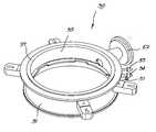
도 4는 본 발명 플랜지의 사시도4 is a perspective view of the present invention flange
도 5는 본 발명 도4의 평면구성도5 is a plan view of the present invention Figure 4
도 6은 본 발명 도4의 일부단면구성도Figure 6 is a partial cross-sectional view of the present invention Figure 4
도 7은 본 발명 도6의 일부 확대도
도 8은 본 발명의 일부확대평단면도7 is an enlarged view of a portion of the present invention Figure 6
Figure 8 is an enlarged partial cross-sectional view of the present invention
<도면의 주요부분에 대한 부호의 설명><Description of the symbols for the main parts of the drawings>
10:외부튜브11:오링10: Outer tube 11: O-ring
20:내부튜브30:플랜지20: inner tube 30: flange
31:외벽면32:수조31: Outer wall surface 32: Water tank
33:유입구34:배출구33: inlet 34: outlet
35:내벽면36:설치홈35: inner wall 36: mounting groove
37:차단판38:배기구37: blocking plate 38: exhaust vent
39:환형돌기40:보트39: annular protrusion 40: boat
40a:슬롯41:웨이퍼
50:단열재51:가스유입구
52:가스배출구40a: Slot 41: Wafer
50: insulation 51: gas inlet
52: gas outlet
삭제delete
본 발명은 반도체 저압화학기상증착(Low Pressure Chemical Vapor Deposition:LP-CVD) 설비의 플랜지에 관한 것으로, 더욱 상세하게는 플랜지를 이중관체형으로 형성하면서도 그 내부에는 내,외부의 온도를 차단토록 하는 단열수단을 갖춤으로써 웨이퍼(Wafer)의 표면상에 가스입자의 균일한 증착이 이루어지도록 함은 물론이고 두터운 막도 균일하게 증착이 이루어지도록 하는 반도체 저압화학기상증착 설비의 플랜지에 관한 것이다.The present invention relates to a flange of a semiconductor Low Pressure Chemical Vapor Deposition (LP-CVD) facility, and more particularly, to form a double-tubular flange and to insulate the inside and outside of the temperature inside the flange. The present invention relates to a flange of a semiconductor low pressure chemical vapor deposition apparatus which has a means for uniform deposition of gas particles on the surface of a wafer as well as for uniform deposition of thick films.
일반적으로 화학기상증착(CVD)은 상압이나 저압 또는 플라즈마 등의 특정한 상태를 형성하고 있는 챔버의 내부에 막의 재료가 되는 여러 가지 가스들을 공급하여 웨이퍼의 표면상에 요구되는 재질의 막을 증착시키도록 하는 공정이다.In general, chemical vapor deposition (CVD) is a method of depositing a film of a desired material on the surface of a wafer by supplying a variety of gases that are the material of the film to the interior of the chamber forming a specific state, such as atmospheric pressure, low pressure or plasma It is a process.
상기 웨이퍼는 실리콘으로 만든 얇은 원판 형태의 반도체 칩의 원판으로서 이 실리콘 웨이퍼의 표면에 도전층 및 절연층 등의 얇은 막을 증착함과 동시에 회 로를 구성하여 전기적 동작이 가능토록 하는 것이다.The wafer is a disk of a semiconductor chip in the form of a thin disk made of silicon, and a thin film such as a conductive layer and an insulating layer is deposited on the surface of the silicon wafer, and a circuit is formed to enable electrical operation.
따라서, 상기한 화학기상증착 공정 중에서 챔버의 내부를 저압상태로 형성하여 공정을 진행토록 하는 것이 일명 저압화학기상증착(LPCVD)이라 할 수 있으며, 이의 일반적인 구성을 살펴보면 도1에서 보는 바와 같다.Therefore, in the chemical vapor deposition process, the interior of the chamber may be referred to as low pressure chemical vapor deposition (LPCVD) to proceed with the process by forming the inside of the chamber in a low pressure state, and a general configuration thereof is shown in FIG. 1.
도1에서 참조되듯이 공정을 위한 챔버(1)는 석영 재질로 형성되는 외측튜브(2)와 내측튜브(3)가 이중으로 형성되어 있고, 하부에는 이들을 지지고정토록 하는 플랜지(4)가 설치되어 있다.As shown in Figure 1, the chamber 1 for the process is formed of a double outer tube (2) and inner tube (3) formed of a quartz material, the lower flange is installed to support them It is.
즉, 상기 플랜지(4)는 소정의 직경을 가지는 금속재질의 관체형상으로 형성되면서 내측면에는 내향 돌출되는 환형돌기가 형성되어 내부튜브(3)가 장착되고, 상단부에는 외측튜브(2)가 올려져 밀착 체결된다.That is, the flange (4) is formed in a tubular shape of a metal material having a predetermined diameter while the inner surface is formed with an annular projection protruding inward to the inner tube (3) is mounted, the upper end of the outer tube (2) is raised Tightly tightened.
또한 상기 플랜지(4)의 일측에는 내부와 연통되면서 증착가스가 출입되는 가스유입구(4a) 및 가스배출구(4b)가 각각 형성되어 있음과 동시에 하부에는 다수 개의 웨이퍼(5)가 슬롯(6a)에 의해 장착되는 보트(boat:6)가 승강가능토록 설치되어 있다.
상기 보트(6)는 도면에서는 미도시되어 있지만 별도의 승강장치에 의해 승강작동되도록 구성되고, 도8에서 더욱 상세히 나타낸 바아 같이 보트(6)의 상부에는 다수 개의 슬롯(6a)이 수직방향으로 설치되어 원판형으로 이루어지는 웨이퍼(5)들을 적층 설치하게 된다.
따라서, 이같이 구성되는 종래의 저압 화학기상증착장치는 웨이퍼(5)들이 보트(6)의 슬롯(6a)에 장착된 상태에서 이의 보트(6)가 별도의 승강장치에 의해 상승작동되어 내측튜브(3)의 내부로 진입하게 됨과 동시에 플랜지(4)의 하단부에 밀착됨으로써 내부를 밀폐된 공간으로 형성하게 된다.In addition, a
Although not shown in the figure, the
Therefore, in the conventional low pressure chemical vapor deposition apparatus configured as described above, the
삭제delete
이러한 상태에서 가스배출구(4b)를 통하여 챔버(1)의 내부를 진공상태로 유지한 다음, 대상이 되는 증착가스를 가스유입구(4a)를 통해 유입시킴과 동시에 외측튜브(2)의 외연에 형성된 가열부(미도시됨)를 가동함으로써 슬롯(6a)에 적층된 웨이퍼(5)의 표면상에 화학성분의 얇은 질화막이 증착되는 것이고, 이때 증착가스는 내측투브(3)의 상단부를 거쳐 내,외측튜브(2)(3)의 사이를 통하여 가스배출구(4b)로 배출되는 것이다.In such a state, the inside of the chamber 1 is maintained in a vacuum state through the gas outlet 4b, and then a target deposition gas is introduced through the
그러나 이와 같이 구성되는 종래의 화학기상증착장치에 있어서는 플랜지의 구조적인 특성상 여러 가지 문제점이 야기되고 있다.However, in the conventional chemical vapor deposition apparatus configured as described above, various problems are caused due to the structural characteristics of the flange.
즉, 챔버(1)의 내부에는 약 800℃ 정도의 고온이 형성됨에 따라 내,외부의 온도차이로 인하여 금속재질로 이루어지는 플랜지의 내벽면에는 가장 심한 열변화를 가져오게 되고, 이에 따라 웨이퍼(5) 뿐만 아니라 플랜지(4)의 내벽면에도 많은 증착이 이루어지게 된다.That is, as the high temperature of about 800 ° C. is formed inside the chamber 1, the most significant heat change is brought to the inner wall surface of the flange made of metal due to the temperature difference between the inside and the outside. As well as a lot of deposition is made on the inner wall surface of the flange (4).
이같이 웨이퍼(5) 외에 원하지 않는 부위에 가스입자가 달라붙어 막이 형성되며, 이는 상대적으로 웨이퍼(5)보다는 결합력이 낮기 때문에 공정이 완료된 후 진공상태가 해제되는 과정에서 외부공기가 유입될 때, 이 막들이 일부 낙하되면서 웨이퍼의 표면으로 낙하되어 불량을 초래하게 된다.As such, a film is formed by adhering gas particles to an unwanted portion other than the
즉, 웨이퍼 측으로 낙하되는 막들로 인하여 균일한 표면을 유지하지 못하여 후공정에 치명적인 악영향을 미치게 되는 것으로, 이러한 경우 튜브 내부의 장비에 증착된 막, 이를테면 육안으로 거의 보이지 않을 정도의 미립자(article)들이 마치 그을음과 같이 웨이퍼의 표면으로 낙하되어 악영향을 미치게 되는 것이다.That is, the films falling to the wafer side do not maintain a uniform surface, which has a fatal adverse effect on post-processing. In this case, the films deposited on the equipment inside the tube, for example, particles that are almost invisible to the naked eye Like soot, it falls to the surface of the wafer and adversely affects it.
또한, 상기와 같이 원하지 않는 부위에 증착이 이루어질 경우 초기에는 아주 얇은 막 상태이므로 자체 하중이 높지 않아 낙하되는 경우가 적지만, 공정 반복될수록 그 두께가 점차적으로 증가되어 낙하확률이 높아지는 문제점이 있는 것이다.In addition, when the deposition is performed on an unwanted portion as described above, since the initial state is a very thin film, its own load is not high, so it is less likely to fall, but as the process is repeated, the thickness thereof is gradually increased to increase the drop probability. .
이러한 현상을 방지하기 위하여 종래에는 공정을 몇 회 반복한 후, 작업을 중지한 상태(다운 타임:Down Time)에서 내부를 세정하는 작업을 필수적으로 행하였 기 때문에 생산성 저하 등 경제적인 손실을 초래하게 되는 문제점이 있었다.In order to prevent such a phenomenon, conventionally, since the process is repeatedly performed several times, and the inside is cleaned in a state where the operation is stopped (down time), an economic loss such as a decrease in productivity is caused. There was a problem.
특히, 이같이 주기적, 반복적인 세정작업에도 불구하고 일부 이물질이 웨이퍼상에 달라붙게 되므로 불량율의 증가는 필연적일 수 밖에 없는 중대한 문제점이 있는 것이었다.In particular, in spite of such periodic and repetitive cleaning operations, some foreign matters stick to the wafer, so that an increase in defect rate is inevitably a serious problem.
본 발명은 상기와 같은 종래의 여러 가지 문제점을 고려하여 이루어진 것으로, 그 목적은 저압 화학기상증착장치의 플랜지를 이중관체로 형성함과 동시에 이들 사이에는 단열재를 설치하여 내,외부의 온도를 차단함으로써 균일한 온도와 압력으로 웨이퍼상에 고른 가스막의 증착을 기대할 수 있도록 하는 반도체 저압화학기상증착 설비의 플랜지를 제공함에 있다.The present invention has been made in consideration of the above-mentioned various problems. The object of the present invention is to form a flange of a low pressure chemical vapor deposition apparatus into a double tube, and at the same time install a heat insulating material therebetween to block internal and external temperature uniformly. The present invention provides a flange of a semiconductor low pressure chemical vapor deposition apparatus which can expect deposition of an even gas film on a wafer at a temperature and pressure.
이러한 목적을 달성하기 위한 본 발명은 반도체 저압화학기상증착 설비의 플랜지를 개선함으로써 달성되는 것으로, 상기 플랜지는 그 벽면을 상부가 개구되는 이중의 관으로 형성하면서도 이들 사이의 설치공간에 별도의 단열재를 설치하여 상부에서 차단판으로 밀폐하고, 또한 상기 설치공간의 일측에는 공기배기구를 형성하여 열에 의해 단열재가 팽창시 내부압력이 해소될 수 있도록 구성함으로써 플랜지의 내부 온도를 항상 균일하게 유지하여 불필요한 증착이 이루어지는 것을 방지토록 함을 특징으로 하는 것이다.The present invention for achieving this object is achieved by improving the flange of the semiconductor low-pressure chemical vapor deposition equipment, the flange is formed of a double tube that the upper surface of the opening while the separate insulating material between the installation space between them It is installed and sealed at the top with a blocking plate, and on one side of the installation space, an air vent is formed so that the internal pressure can be released when the heat insulator is expanded by heat. It is characterized by preventing from being made.
이하에서 본 발명의 바람직한 실시예를 첨부된 도면에 의하여 상세히 설명하면 다음과 같다.Hereinafter, described in detail with reference to the accompanying drawings a preferred embodiment of the present invention.
첨부된 도면의 도2 및 도3에서는 본 발명의 플랜지가 적용되는 반도체 저압화학기상증착장치의 일부를 나타낸 도면이고, 도4 이하에서는 본 발명의 플랜지를 상세히 나타내고 있다.2 and 3 of the accompanying drawings is a view showing a part of a semiconductor low pressure chemical vapor deposition apparatus to which the flange of the present invention is applied, Figure 4 or below shows the flange of the present invention in detail.
상기 저압화학기상증착장치는 도면에서 보듯이 밀폐형의 외부튜브(10)와 이의 내부에 이중으로 설치되는 내부튜브(20)와, 상기 내,외튜브(10)(20)의 하부에 설치되어 이들을 지지토록 하는 플랜지(30)와, 상기 플랜지(30)의 하부에서 승강작동되면서 웨이퍼를 적층한 보트(40)로 구성된다.The low pressure chemical vapor deposition apparatus is installed in the lower
상기 내,외부튜브(10)(20)는 플랜지(30)의 상부에 설치되어 이에 지지되는 것으로, 상기 플랜지(30)는 금속재질로 이루어지면서 소정 직경을 가지는 이중의 관체형으로 형성된다.The inner and
플랜지(30)는 외벽면(31)의 상단부에 외부튜브(10)가 밀착체결되면서 외주연을 따라 냉각수가 저수되어 상단 결합부의 오링(11)을 냉각시키도록 하는 수조(32)가 갖추어져 구성된다,The
상기 수조(32)의 냉각수는 플랜지(30)와 외부튜브(10) 사이에 기밀을 유지토록 설치되는 오링(11)의 열변형을 방지하기 위한 것이며, 일측에는 수조(32)내로 냉각수를 유입토록 하는 유입구(33)와 냉각수를 배출토록 하는 배출구(34)가 형성된다.The cooling water of the
또한, 외벽면(31)의 내부에는 내벽면(35)이 형성되면서 이들 사이에는 상향 개구되는 설치홈(36)이 형성되고, 이 설치홈(36)에는 단열성을 뛰어난 석영 등의 재질로 이루어지는 단열재(50)가 설치된다.In addition, an
즉, 상기 설치홈(36)은 외벽면(31)과 내벽면(35)에 의해 상향 개구되는 형태로 설치되어 별도의 단열재(50)가 설치되는 것이며, 이의 단열재(50)는 석영 재질 뿐만 아니라 내열성과 단열성이 뛰어난 여러 가지 재질로 형성되어 내,외부의 온도를 차단하게 된다.That is, the
또한, 상기 설치홈(36)의 상단에는 별도의 차단판(37)이 용접 등의 방법으로 체결되어 설치홈(36)을 밀폐시키게 되고, 상기 설치홈(36)의 일측 소정에는 내부에서 단열재(50)가 고온에 의해 팽창시 압력을 해소토록 하는 배기구(38)가 형성된다.In addition, a
상기 배기구(38)는 설치홈(36)내에 발생되는 고압을 외부로 해소토록 하기 위한 것으로, 즉 고온에 의해 단열재(50)가 열팽창되는 경우 압력이 지나치게 증가하여 터질 수 있는 것을 미연에 방지하기 위한 것이며, 적어도 하나 이상 설치하는 것이 요구된다.The
또한, 상기 플랜지(30)의 하부 일측에는 내부로 가스를 유입토록 하는 가스유입구(51)가 설치됨과 동시에 타측에는 가스배출구(52)가 각각 설치되어 챔버의 내부로 웨이퍼에 막을 형성토록 하는 가스를 유입 및 배출시키게 된다.In addition, a
그리고, 상기 플랜지(30)의 하부에는 도8에서 보듯이 원판형의 웨이퍼(41)를 슬롯(40a)에 적층하여 내,외부튜브(10)(20)내로 출입시키도록 하는 보트(40)가 통상에서와 같이 설치되고, 이 보트(40)는 미도시된 별도의 엘레베이터에 의해 승강작동된다.In the lower portion of the
한편, 도면중 미설명 부호 39는 플랜지의 외벽면 내부에 내향 돌출되게 설치되는 환형돌기로서 이는 내부튜브(20)가 설치되는 기능을 제공하게 된다.On the other hand,
이와 같이 구성되는 본 발명은 플랜지(30)의 상부에 내,외튜브(10)(20)가 각각 설치됨과 동시에 하부에는 보트(40)가 설치되고, 상기 외부튜브(10)의 외주연에는 미도시된 가열부가 설치된다.In the present invention configured as described above, the inner and
따라서, 튜브내에 웨이퍼를 넣고 내부를 고온/진공상태로 만든 후 대상이 되는 가스를 충진하여 웨이퍼의 표면상에 그 가스에 포함된 화학성분들을 얇은 막으로 증착하도록 하는 것이다.Therefore, the wafer is placed in a tube, and the inside is made hot / vacuum state, and then the target gas is filled to deposit a chemical film contained in the gas on the surface of the wafer in a thin film.
즉, 웨이퍼(41)들이 보트(40)의 슬롯(40a)에 다수 개가 장착된 상태에서 상기 보트(40)가 별도의 엘리베이터와 같은 승강장치에 의해 서서히 상승되어 내부튜브(20)의 내측으로 이동하게 되면 챔버의 내부는 밀폐된 상태를 유지하게 된다.That is, in a state where a plurality of
이어서 도면중 미도시된 가열부(외부튜브의 외측에 설치됨)가 가열되면서 튜브 내측의 온도를 약800℃ 정도로 유지하게 됨과 동시에, 진공펌프를 통하여 튜브 내부의 공기를 배출시켜 챔버내를 진공상태로 유지하게 된다.Subsequently, the heating unit (not provided in the outer tube), which is not shown in the drawing, is heated to maintain the temperature inside the tube at about 800 ° C., and the air inside the tube is discharged through the vacuum pump to bring the chamber into a vacuum state. Will be maintained.
이는 내부에 잔류하는 공기 중에 포함된 산소, 이산화탄소, 질소, 수분 등과 같은 불순물의 영향을 최소화하기 위한 것으로 즉, 열전달물질인 공기를 최대한 제거하여 튜브내의 온도편차를 줄이기 위함이다.This is to minimize the influence of impurities such as oxygen, carbon dioxide, nitrogen, moisture, etc. contained in the air remaining inside, that is to reduce the temperature deviation in the tube by removing the air as a heat transfer material as much as possible.
챔버내의 진공이 이루어지고 나면 가스유입구(51)를 통해 가스(SiH2CL2, NH3, SiH4, N2O 등)를 주입함으로써 이 가스가 도면의 화살표와 같이 이동되면서 화확적인 반응이 일어나게 되어 슬롯(40a)에 적층된 웨이퍼(41)의 표면상에 막을 증착시키게 된다.After the vacuum in the chamber is made, the gas (SiH2CL2, NH3, SiH4, N2O, etc.) is injected through the
이때, 상기 챔버내에는 고온/고압이 유지되는 것이나, 본 발명에 의한 단열수단에 의해 외부온도에 의한 영향을 최대한 받지 않고 고른 온도와 압력을 유지하게 됨으로써 증착효율을 향상시키게 된다.At this time, the high temperature / high pressure is maintained in the chamber, by the heat insulating means according to the present invention to maintain the even temperature and pressure without being influenced by the external temperature as much as possible to improve the deposition efficiency.
즉, 플랜지(30)가 금속재질로 이루어짐에 따라 열변화가 가장 심한 플랜지의 벽면내에 단열수단을 포켓형태의 설치홈(36)을 형성하고, 이의 설치홈(36)내에 단열효과가 우수한 단열재(50)를 설치하여 열변화를 최소화함으로써 챔버내의 고른 열로 인하여 증착효율을 증대시키게 된다
이때 증착가스는 내부튜브(20)의 상단을 거쳐 내,외부튜브(10)(20) 사이의 공간을 통하여 가스배출구(52)로 배출되는 것이고, 이같이 증착이 모두 완료되면, 전술한 역순의 작동에 의해 챔버내를 대기압으로 만든 후 보트(40)를 하강시켜 웨이퍼(41)를 회수함으로써 일련의 증착공정이 완료되는 것이다.That is, as the
At this time, the deposition gas is discharged to the
삭제delete
이상 상세히 설명한 바와 같이 본 발명은 플랜지의 벽면을 이중관체로 형성하면서도 그 내부에 단열재를 설치하여 내,외부의 온도를 차단함으로써 웨이퍼 표면상에 막을 증착시 챔버내의 온도와 압력을 고르게 유지할 수가 있다.As described in detail above, the present invention can maintain the temperature and pressure in the chamber even when the film is deposited on the wafer surface by blocking the internal and external temperatures by forming a heat insulating material therein while forming the wall of the flange as a double tube.
따라서, 플랜지의 내벽면에 불필요하게 증착되는 막질이 웨이퍼 표면에 낙하되는 등의 불량발생 원인을 근본적으로 제거할 수 있는 효과를 가지게 될 뿐만 아니라, 웨이퍼 표면에 증착되는 막의 두께를 균일하고도 고르게 유지할 수 있는 효과를 가지게 된다.Therefore, the film quality deposited on the inner wall surface of the flange not only has the effect of fundamentally eliminating the cause of defects such as falling on the wafer surface, but also maintains the thickness of the film deposited on the wafer surface uniformly and evenly. Will have the effect.
또한, 플랜지의 세정작업에 따라 햇수와 시간을 최대한 줄일 수 있는 효과와 더불어 세정작업시 발생되는 폐기물 역시 최대한 줄일 수 있는 등의 효과를 가지게 되는 것이다.In addition, according to the cleaning operation of the flange as well as the effect of reducing the number of years and time as well as the waste generated during the cleaning operation to have the effect of reducing as much as possible.
Claims (1)
Translated fromKoreanPriority Applications (1)
| Application Number | Priority Date | Filing Date | Title |
|---|---|---|---|
| KR1020050105385AKR100715689B1 (en) | 2005-11-04 | 2005-11-04 | Flange of Semiconductor Low Pressure Chemical Vapor Deposition Equipment |
Applications Claiming Priority (1)
| Application Number | Priority Date | Filing Date | Title |
|---|---|---|---|
| KR1020050105385AKR100715689B1 (en) | 2005-11-04 | 2005-11-04 | Flange of Semiconductor Low Pressure Chemical Vapor Deposition Equipment |
Related Child Applications (1)
| Application Number | Title | Priority Date | Filing Date |
|---|---|---|---|
| KR2020050031363UDivisionKR200406614Y1 (en) | 2005-11-04 | 2005-11-04 | Flange of Semiconductor Low Pressure Chemical Vapor Deposition Equipment |
Publications (1)
| Publication Number | Publication Date |
|---|---|
| KR100715689B1true KR100715689B1 (en) | 2007-05-09 |
Family
ID=38270023
Family Applications (1)
| Application Number | Title | Priority Date | Filing Date |
|---|---|---|---|
| KR1020050105385AActiveKR100715689B1 (en) | 2005-11-04 | 2005-11-04 | Flange of Semiconductor Low Pressure Chemical Vapor Deposition Equipment |
Country Status (1)
| Country | Link |
|---|---|
| KR (1) | KR100715689B1 (en) |
Citations (2)
| Publication number | Priority date | Publication date | Assignee | Title |
|---|---|---|---|---|
| KR20190000940A (en)* | 2016-05-27 | 2019-01-03 | 마코 서지컬 코포레이션 | Pre-operative planning and associated post-operative registration for the surgical system |
| KR20190000980A (en)* | 2017-06-26 | 2019-01-04 | 이동원 | A personal Healthcare System |
- 2005
- 2005-11-04KRKR1020050105385Apatent/KR100715689B1/enactiveActive
Patent Citations (2)
| Publication number | Priority date | Publication date | Assignee | Title |
|---|---|---|---|---|
| KR20190000940A (en)* | 2016-05-27 | 2019-01-03 | 마코 서지컬 코포레이션 | Pre-operative planning and associated post-operative registration for the surgical system |
| KR20190000980A (en)* | 2017-06-26 | 2019-01-04 | 이동원 | A personal Healthcare System |
Non-Patent Citations (2)
| Title |
|---|
| 2019940022677 (공개번호) |
| 2019980005323A |
Similar Documents
| Publication | Publication Date | Title |
|---|---|---|
| TWI389204B (en) | Semiconductor device manufacturing method, substrate processing device, and substrate processing method | |
| US10229845B2 (en) | Substrate treatment apparatus | |
| TWI415188B (en) | Collecting unit for semiconductor process | |
| US9816183B2 (en) | Substrate processing apparatus | |
| US8683943B2 (en) | Plasma process apparatus and plasma process method | |
| KR101291957B1 (en) | Film formation apparatus, operation method thereof, and memory medium for executing the method | |
| WO2006132274A1 (en) | Sealing structure of vacuum device | |
| US10907252B2 (en) | Horizontal heat choke faceplate design | |
| CN110870050A (en) | Substrate processing apparatus, quartz reaction tube, cleaning method, and program | |
| KR100554113B1 (en) | Cleaning method of film forming apparatus, cleaning mechanism and film forming apparatus thereof | |
| US11732358B2 (en) | High temperature chemical vapor deposition lid | |
| US20190226088A1 (en) | High temperature faceplate with thermal choke and cooling | |
| US20190226087A1 (en) | Heated ceramic faceplate | |
| US20180105933A1 (en) | Substrate processing apparatus and method for cleaning chamber | |
| KR200406614Y1 (en) | Flange of Semiconductor Low Pressure Chemical Vapor Deposition Equipment | |
| KR100393751B1 (en) | How to make a film | |
| KR100715689B1 (en) | Flange of Semiconductor Low Pressure Chemical Vapor Deposition Equipment | |
| JP2004273605A (en) | Substrate processing equipment | |
| KR100752148B1 (en) | Substrate processing equipment | |
| JP2009016426A (en) | Semiconductor device manufacturing method and substrate processing apparatus | |
| JP4404666B2 (en) | Substrate support, substrate processing apparatus, and semiconductor device manufacturing method | |
| KR20090055347A (en) | Nozzle Unit and Atomic Layer Deposition Equipment with the Unit | |
| JP2003051452A (en) | Semiconductor device manufacturing method and substrate processing apparatus | |
| JP2003051533A (en) | Semiconductor device manufacturing method and substrate processing apparatus | |
| JP2012253134A (en) | Substrate processing apparatus |
Legal Events
| Date | Code | Title | Description |
|---|---|---|---|
| A201 | Request for examination | ||
| PA0109 | Patent application | Patent event code:PA01091R01D Comment text:Patent Application Patent event date:20051104 | |
| PA0201 | Request for examination | ||
| E902 | Notification of reason for refusal | ||
| PE0902 | Notice of grounds for rejection | Comment text:Notification of reason for refusal Patent event date:20061108 Patent event code:PE09021S01D | |
| E701 | Decision to grant or registration of patent right | ||
| PE0701 | Decision of registration | Patent event code:PE07011S01D Comment text:Decision to Grant Registration Patent event date:20070417 | |
| GRNT | Written decision to grant | ||
| PR0701 | Registration of establishment | Comment text:Registration of Establishment Patent event date:20070501 Patent event code:PR07011E01D | |
| PR1002 | Payment of registration fee | Payment date:20070502 End annual number:3 Start annual number:1 | |
| PG1601 | Publication of registration | ||
| PR1001 | Payment of annual fee | Payment date:20100430 Start annual number:4 End annual number:4 | |
| PR1001 | Payment of annual fee | Payment date:20110215 Start annual number:5 End annual number:5 | |
| PR1001 | Payment of annual fee | Payment date:20120523 Start annual number:6 End annual number:6 | |
| FPAY | Annual fee payment | Payment date:20130222 Year of fee payment:7 | |
| PR1001 | Payment of annual fee | Payment date:20130222 Start annual number:7 End annual number:7 | |
| FPAY | Annual fee payment | Payment date:20140227 Year of fee payment:8 | |
| PR1001 | Payment of annual fee | Payment date:20140227 Start annual number:8 End annual number:8 | |
| FPAY | Annual fee payment | Payment date:20150429 Year of fee payment:9 | |
| PR1001 | Payment of annual fee | Payment date:20150429 Start annual number:9 End annual number:9 | |
| FPAY | Annual fee payment | Payment date:20160317 Year of fee payment:10 | |
| PR1001 | Payment of annual fee | Payment date:20160317 Start annual number:10 End annual number:10 | |
| FPAY | Annual fee payment | Payment date:20170425 Year of fee payment:11 | |
| PR1001 | Payment of annual fee | Payment date:20170425 Start annual number:11 End annual number:11 | |
| FPAY | Annual fee payment | Payment date:20190502 Year of fee payment:13 | |
| PR1001 | Payment of annual fee | Payment date:20190502 Start annual number:13 End annual number:13 | |
| PR1001 | Payment of annual fee | Payment date:20200629 Start annual number:14 End annual number:14 | |
| PR1001 | Payment of annual fee | Payment date:20210429 Start annual number:15 End annual number:15 | |
| PR1001 | Payment of annual fee | Payment date:20220502 Start annual number:16 End annual number:16 | |
| PR1001 | Payment of annual fee | Payment date:20230601 Start annual number:17 End annual number:17 | |
| PR1001 | Payment of annual fee | Payment date:20240502 Start annual number:18 End annual number:18 |