KR100714531B1 - Broadband Wire Grid Polarizers for the Visible Spectrum - Google Patents
Broadband Wire Grid Polarizers for the Visible SpectrumDownload PDFInfo
- Publication number
- KR100714531B1 KR100714531B1KR1020017016236AKR20017016236AKR100714531B1KR 100714531 B1KR100714531 B1KR 100714531B1KR 1020017016236 AKR1020017016236 AKR 1020017016236AKR 20017016236 AKR20017016236 AKR 20017016236AKR 100714531 B1KR100714531 B1KR 100714531B1
- Authority
- KR
- South Korea
- Prior art keywords
- substrate
- polarizer
- refractive index
- region
- ribs
- Prior art date
- Legal status (The legal status is an assumption and is not a legal conclusion. Google has not performed a legal analysis and makes no representation as to the accuracy of the status listed.)
- Expired - Fee Related
Links
Images


Classifications
- G—PHYSICS
- G02—OPTICS
- G02B—OPTICAL ELEMENTS, SYSTEMS OR APPARATUS
- G02B5/00—Optical elements other than lenses
- G02B5/30—Polarising elements
- G—PHYSICS
- G02—OPTICS
- G02B—OPTICAL ELEMENTS, SYSTEMS OR APPARATUS
- G02B5/00—Optical elements other than lenses
- G02B5/30—Polarising elements
- G02B5/3025—Polarisers, i.e. arrangements capable of producing a definite output polarisation state from an unpolarised input state
- G02B5/3058—Polarisers, i.e. arrangements capable of producing a definite output polarisation state from an unpolarised input state comprising electrically conductive elements, e.g. wire grids, conductive particles
- G—PHYSICS
- G02—OPTICS
- G02B—OPTICAL ELEMENTS, SYSTEMS OR APPARATUS
- G02B5/00—Optical elements other than lenses
- G02B5/18—Diffraction gratings
- G02B5/1809—Diffraction gratings with pitch less than or comparable to the wavelength
Landscapes
- Physics & Mathematics (AREA)
- General Physics & Mathematics (AREA)
- Optics & Photonics (AREA)
- Polarising Elements (AREA)
- Liquid Crystal (AREA)
Abstract
Translated fromKoreanDescription
Translated fromKorean본 발명은 전자기 스펙트럼의 가시영역에 사용하는 광학 요소를 편광시키는데 관련된다. 특히 본 발명은 직교편광의 빛을 효과적으로 반사시키는 동안에 특정한 편광 빛을 효과적으로 투과시키는 광대역 와이어 그리드 편광자에 관련된다.The present invention relates to polarizing optical elements for use in the visible region of the electromagnetic spectrum. In particular, the present invention relates to a broadband wire grid polarizer that effectively transmits certain polarized light while effectively reflecting light of orthogonal polarization.
무선 파형을 편광시키기 위한 평행 전도 와이어 어레이(array)의 사용은 약 110년 전으로 거슬러 올라간다. 통상적으로 투명 기질에 의해 지지되는 얇은 평행 전도체 어레이 형식인 와이어 그리드는 전자기 스펙트럼의 적외선 영역에 대한 편광자로 사용되어져 왔다.The use of parallel conducting wire arrays to polarize radio waves dates back about 110 years. Wire grids, typically in the form of thin parallel conductor arrays supported by transparent substrates, have been used as polarizers for the infrared region of the electromagnetic spectrum.
와이어 그리드 편광자 성능을 결정하는 중요한 요소는 평행 그리드 요소의 중앙 대 중앙 간격 혹은 주기와 입사 방사선의 파장 사이의 관계이다. 만약 그리드 간격 혹은 주기가 파장에 비교해 볼 때 길다면, 편광자보다는 회절격자의 기능으로 그리드는 종래의 원리에 따라 편광을 회절시킨다. 만약 그리드 간격 혹은 주기가 파장보다 짧다면, 그리드는 그리드 요소에 평행하게 편광된 전자기 방사를 반사시키고, 직교 편광의 방사를 투과시키는 역할을 한다.An important factor in determining wire grid polarizer performance is the relationship between the center to center spacing or period of parallel grid elements and the wavelength of the incident radiation. If the grid spacing or period is long compared to the wavelength, the grid diffracts the polarization according to conventional principles as a function of the diffraction grating rather than the polarizer. If the grid spacing or period is shorter than the wavelength, the grid serves to reflect electromagnetic radiation polarized parallel to the grid element and to transmit radiation of orthogonal polarization.
그리드 주기가 대략 파장의 절반에서 두배의 범위 내에 있는 전이 영역은 그리드의 투과 및 반사 특성의 갑작스런 변화로 나타난다. 특히, 그리드 요소에 대해 직교 편광된 빛에 대해서 편광된 갑작스런 반사율의 증가와 그에 상응하는 투과율 감소는 정해진 입사각에서 하나 이상의 특정한 파장에서 일어난다. 이러한 효과는 우드(Wood)에 의해 1902년에(Philosophical Magazine, 1902년 9월) 최초로 보고되었고, "우드 변이(anomalies)"라고 불린다. 레일리(Rayleigh)는 우드 데이터를 분석했고, 높은 회절 차수가 나타나는(Philosophical Magazine, vol14(79), 페이지 60-65, 1907년 7월) 각도 및 파장의 조합에서 변이가 일어난다는 통찰력을 갖고 있었다. 레일리는 변이(통상적으로"레일리 공명"이라고도 불림)의 위치를 추정하기 위해 다음과 같은 방정식을 만들어냈다.Transition regions with grid periods in the range of approximately half to twice the wavelength appear as sudden changes in the transmission and reflection properties of the grid. In particular, the sudden increase in polarized light and the corresponding decrease in transmittance for light orthogonally polarized with respect to the grid element occur at one or more specific wavelengths at a given angle of incidence. This effect was first reported by Wood in 1902 (Philosophical Magazine, September 1902) and is called "anomalies". Rayleigh analyzed the wood data and had the insight that the variation occurs at a combination of angles and wavelengths that show high diffraction orders (Philosophical Magazine, vol 14 (79), pages 60-65, July 1907). Rayleigh created the following equation to estimate the location of the mutation (commonly called "Rail resonance"):

ε는 회절 주기;ε is the diffraction period;
n은 격자를 둘러싼 매질의 굴절률;n is the refractive index of the medium surrounding the grating;
k는 나타나는 회절된 항목의 차수에 상응하는 정수;k is an integer corresponding to the order of the diffracted item appearing;
λ과 Θ은 공명이 일어나는 파장 및 입사각(둘다 공기에서 측정됨)이다.λ and Θ are the wavelength at which resonance occurs and the angle of incidence (both measured in air).
절연 기질의 한 측면에 형성된 격자의 경우, 상기 공식의 n은 1 혹은 기질 재료의 굴절률과 동일할 수 있다. 공명이 일어나는 가장 긴 파장은 다른 공식으로 주어진다.In the case of a grating formed on one side of an insulating substrate, n in the formula may be equal to 1 or the refractive index of the substrate material. The longest wavelength at which resonance occurs is given by another formula.

여기서 n은 기질의 굴절률로 고정된다.Where n is fixed to the refractive index of the substrate.
각도 의존도의 효과는 각도가 증가함에 따라 투과 영역을 더 넓은 파장으로 이동시킨다. 편광자를 편광 회전 거울 혹은 편광 광선 분할기로 사용하고자 할 때 이와 같은 사실은 매우 중요하다.The effect of angle dependence shifts the transmission region to a wider wavelength as the angle increases. This is very important when using a polarizer as a polarization rotating mirror or polarization beam splitter.
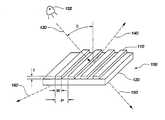
도 1은 종래 기술의 기본적인 와이어 그리드 편광자를 도시하고, 종래 기술 및 본 발명에 관한 일련의 사례들에 사용될 용어들을 정의한다. 와이어 그리드 편광자(100)는 절연 기질(120)에 의해 지지되는 여러개의 평행한 전도성 전극(110)으로 구성된다. 이 장치는 전도체의 주기 혹은 피치(pitch), p로 표시; 개별 전도체의 폭, w로 표시; 전도체의 주께, t로 표시된다. 광원(132)에 의해 생성된 빛의 광선(130)은 법선으로부터 각 Θ로 편광자에 입사된다. 이때, 입사 평면은 전도성 요소에 수직이다. 와이어 그리드 편광자(100)는 이러한 광선을 반사 성분(140)과, 비-회절형 투과 성분(150)으로 분할한다. 방정식(2)에 의해 주어진 가장 긴 공명 파장보다 짧은 파장에 대해서, 적어도 하나의 고차 회절 성분(160)이 있을 것이다. S, P 편광에 대한 일반적인 정의를 사용할 때, S 편광을 갖는 빛은 입사평면에 대해 직교인 편광 벡터를 가지므로, 전도성 요소에 평행하다. 반대로, P 편광을 갖는 빛은 입사 평면에 평행인 편광 벡터를 가지므로 전도성 요소에 직교한다.1 shows a basic wire grid polarizer of the prior art and defines terms to be used in the prior art and a series of examples relating to the invention. The
일반적으로 와이어 그리드 편광자는 그리드의 와이어에 평행한 전기장 벡터를 갖는 빛을 반사하고, 그리드의 와이어에 수직한 전기장 벡터를 갖는 빛을 투과시킬 것이지만, 입사평면은 전술된 바와 같이 그리드의 와이어에 수직할 수도 있고 그렇지 않을 수도 있다. 여기서 설명된 기하학적인 표시는 단순히 예시를 위한 것이다.In general, the wire grid polarizer will reflect light having an electric field vector parallel to the wires of the grid and will transmit light having an electric field vector perpendicular to the wires of the grid, but the plane of incidence will be perpendicular to the wires of the grid as described above. It may or may not be. The geometrical representations described herein are for illustration only.
이상적인 시스템에서, 와이어 그리드 편광자는 하나의 빛 편광에 대해 S 편광 빛처럼 완벽한 거울로 기능할 것이고, P 편광 빛처럼 다른 편광에 대해 완벽하게 투명일 것이다. 그러나 실제로 거울로 사용되는 가장 반사성이 큰 금속도 소량의 입사광을 흡수하며 90% 내지 95%정도만을 반사할 뿐이다. 또한 평면 유리는 표면 반사 때문에 100% 모두 입사광을 투과시키지 못한다.In an ideal system, the wire grid polarizer would function as a perfect mirror for S-polarized light for one light polarization and would be completely transparent for other polarizations like P-polarized light. However, the most reflective metal used as a mirror actually absorbs a small amount of incident light and only reflects 90% to 95%. In addition, the flat glass does not transmit
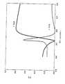
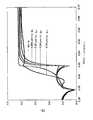
도 2는 45도의 입사각Θ을 갖는 종래 기술의 와이어 그리드 편광자의 연산된 비회절 혹은 영차 투과 및 반사를 도시한다. 이러한 데이터는 Grating Solver Development Company(P.O.Box 353, Allen, Texas)에서 나온 지솔버(Gsolver) 격자 분석 소프트웨어를 사용하여 연산된다. 이러한 소프트웨어는 엄격히 결합된 파동 분석 및 형태법(modal method)을 구현한다. 분석방법 및 결과는 "적외선 및 가시광선에 대한 엽편상 금속 투과 격자의 결합파동 분석(Journal of Optical Society of America, Vol.12 No.5, 페이지 1118-1127, 1995년 5월)이라는 논문에 나온 것과 비슷하다. 이 분석은 주기 p=0.2㎛를 갖는 알루미늄 그리드, 폭 w=0.1㎛를 갖는 전도체, 전도체 두께는 t=0.1㎛, 기질 굴절률 n=1.525를 갖는 것으로 가정한다. 방정식 1에서 예상된 바와 같이 두 개의 공명은 약 0.34㎛과 0.445㎛의 파장에서 발생한다. 이러한 공명은 P 편광에 대한 편광자 특성에만 중요한 영향을 끼친다.Figure 2 illustrates the computed non-diffraction or zero order transmission and reflection of a prior art wire grid polarizer with an angle of incidence Θ of 45 degrees. This data is computed using Gsolver lattice analysis software from the Grating Solver Development Company (P.O.Box 353, Allen, Texas). This software implements tightly coupled wave analysis and modal methods. The analytical methods and results are presented in a paper entitled "The Analysis of the Combined Waves of Lobed Metal Transmission Gratings for Infrared and Visible Light (Journal of Optical Society of America, Vol. 12 No. 5, pages 1118-1127, May 1995). This analysis assumes an aluminum grid with period p = 0.2 μm, conductors with width w = 0.1 μm, conductor thickness t = 0.1 μm and substrate refractive index n = 1.525. As shown, the two resonances occur at wavelengths of about 0.34 μm and 0.445 μm, which only has a significant effect on the polarizer properties for P polarization.
S 방향으로 편광된 입사광의 경우, 종래 기술의 편광자 성능은 이상적인 성능에 가깝다. S 편광에 대한 반사효율은 0.4㎛에서 0.7㎛의 가시 스펙트럼에 대해 90% 이상이다. 이러한 파장 대역에 대해서 2.5% 이하의 S 편광된 빛은 투과되고, 나머지는 흡수된다. 약간의 투과된 성분을 빼면, S 편광에 대한 와이어 그리드 편광자의 특성은 연속적인 알루미늄 거울의 특성과 매우 비슷하다.In the case of incident light polarized in the S direction, the prior art polarizer performance is close to the ideal performance. The reflection efficiency for S-polarized light is more than 90% for the visible spectrum of 0.4 μm to 0.7 μm. For this wavelength band up to 2.5% S polarized light is transmitted and the rest is absorbed. Subtracting some transmitted components, the properties of the wire grid polarizer for S polarized light are very similar to those of continuous aluminum mirrors.
P 편광의 경우, 와이어 그리드의 투과 및 반사 효율은 약 0.5㎛ 이하의 파장의 공명 효과에 의해 영향을 받는다. 0.5㎛보다 긴 파장에서는 와이어 그리드 구조가 P 편광된 빛에 대해 손실형 절연층과 같은 역할을 한다. 이러한 층에서의 손실 및 표면으로부터의 반사는 P 편광된 빛의 투과율을 약 0.5㎛에서 0.7㎛의 파장 대역에 대해서 약 80% 정도로 제한한다.In the case of P polarization, the transmission and reflection efficiencies of the wire grid are affected by the resonance effect of wavelengths of about 0.5 μm or less. At wavelengths longer than 0.5 μm, the wire grid structure acts like a lossy insulation layer for P polarized light. Loss in this layer and reflection from the surface limits the transmission of P polarized light to about 80% for a wavelength band of about 0.5 μm to 0.7 μm.
도 3은 타마다(Tamada)의 미국 특허 제 5,748,368 호에 공지된 바와 같이 종래 기술의 다른 형식 와이어 그리드 편광자의 연산된 성능을 나타낸다. 이러한 경우, 굴절률 일치 유체나 접착제 중 하나가 두개의 기질 사이에 그리드 구조를 적층시키기 위해 사용되어, 그리드는 일정 굴절률의 매질로 둘러쌓인다. 본 예에서, n=1.525 및 그외 다른 그리드 매개변수들은 이전 예와 동일하다. 와이어 그리드 구조는 방정식(1)에서 예상된 바와 같이, 약 0.52㎛의 파장에서의 단일 공명을 나타낸다. P 편광에 대해 반사가 거의 0인 0.58에서 0.62㎛의 좁은 파장 영역이 있다는 점에 주목하여야 한다. 미국 특허 제 5,748,368 호는 높은 소광율을 갖는 협대역폭 와이어 그리드 편광자를 구현하기 위해 이 효과를 이용할 수 있는 와이어 그리드 편광자를 기재하고 있다. 타마다 특허 출원에 나타낸 예들은 550nm의 그리드 주기를 사용하였고, 그리드 두께, 전도체 폭 및 형상, 입사각에 따라 800 내지 950nm의 공명 파장을 발생시켰다. 타마다 특허는 편광 방향에 대한 특별한 정의를 채용한다(P 편광은 그리드 요소에 평행하게 정의되어 종래의 정의에 상관없이 입사평면에 직각이다). 타마다가 이용하는 공명 효과는 방정식(1)에 의해 예상된 위치의 공명과는 다르다. 두 개의 공명이 일치할 수 있지만 꼭 그래야 되는 것은 아니다. 타마다는 이러한 두 번째 공명을 이용한다. 또한, 박막 간섭 효과가 있다. 직교 편광 에 대해 반사율이 겨우 몇 %도 되지 않는 편광자의 대역폭은 통상적으로 중앙 파장의 5%정도이다. 이러한 형식의 협대역 편광자가 광학 메모리와 통신 시스템 등의 분야에 사용되고 있지만, 액정 디스플레이같은 많은 가시광선 시스템들은 400nm에서 700nm의 가시 스펙트럼 파장에 대해 균일한 특성을 갖는 편광 광학 요소를 요구하고 있다.3 shows the calculated performance of another type of wire grid polarizer of the prior art, as known from US Pat. No. 5,748,368 to Tamada. In this case, either a refractive index matching fluid or an adhesive is used to stack the grid structure between the two substrates so that the grid is surrounded by a medium of constant refractive index. In this example, n = 1.525 and other grid parameters are the same as in the previous example. The wire grid structure exhibits a single resonance at a wavelength of about 0.52 μm, as expected in equation (1). It should be noted that there is a narrow wavelength region of 0.58 to 0.62 μm with almost zero reflection for P polarization. U. S. Patent No. 5,748, 368 describes wire grid polarizers that can utilize this effect to implement narrow bandwidth wire grid polarizers with high extinction rates. The examples shown in the Tadama patent application used a grid period of 550 nm, generating a resonance wavelength of 800-950 nm depending on the grid thickness, conductor width and shape, and angle of incidence. The Tamada patent employs a special definition of the polarization direction (P polarization is defined parallel to the grid element and is perpendicular to the plane of incidence regardless of the conventional definition). The resonance effect used by tamada is different from the resonance of the position predicted by equation (1). The two resonances can coincide, but this is not necessary. Tamada uses this second resonance. In addition, there is a thin film interference effect. For orthogonal polarization, the bandwidth of a polarizer with only a few percent reflectance is typically about 5% of the center wavelength. Although narrow band polarizers of this type are used in fields such as optical memories and communication systems, many visible light systems, such as liquid crystal displays, require polarizing optical elements having uniform properties for visible spectral wavelengths of 400 nm to 700 nm.
도 2에 도시된 데이터로 돌아가서, 광대역 편광에 대한 필수사항은 가장 긴 파장 공명 포인트가 사용을 위한 스펙트럼보다 짧은 파장으로 변환되거나 억제되어야 한다는 점이다. 방정식(2)에서, 가장 긴 파장 공명 포인트의 파장은 세 가지 방식으로 줄어들 수 있는 것을 볼 수 있다. 첫째로, 그리드 주기ε가 감소될 수 있다. 그러나 그리드 주기를 감소하는 것은 그리드 구조를 만드는데 대한 어려움을 가중시키는데, 특히, 반사된 편광의 적정 반사율을 보장하기 위해 그리드 요소의 두께가 유지되어야 하기 때문이다. 둘째로, 입사각이 거의 수직인 입사각으로 제한될 수 있다. 그러나, 입사각을 제한하는 것은 편광자 장치의 활용도를 현격히 떨어뜨릴 것이고, 45도를 중심으로 하는 광각 대역폭이 요망되는 투영 액정 표시장치 등의 장비에 사용될 수 없게 한다. 세 번째로, 기질의 굴절률이 낮아질 수 있다. 그러나, 편광자 장치의 대량 생산에 대한 비용효과만을 갖는 기질은 1737F 형식의 코닝(Corning) 혹은 AF45 형식의 스콧(Schott) 같은 몇가지 종류의 얇은 박판 유리인데, 가시 스펙트럼에 대해 약 1.5에서 1.53 사이에서 변하는 굴절률을 갖는다.Returning to the data shown in FIG. 2, a requirement for broadband polarization is that the longest wavelength resonance point must be converted or suppressed to a wavelength shorter than the spectrum for use. In equation (2), it can be seen that the wavelength of the longest wavelength resonance point can be reduced in three ways. First, the grid period ε can be reduced. However, reducing the grid period adds to the difficulty of creating a grid structure, in particular because the thickness of the grid elements must be maintained to ensure proper reflectivity of the reflected polarized light. Secondly, the angle of incidence can be limited to an angle of incidence that is nearly vertical. However, limiting the angle of incidence will drastically reduce the utilization of the polarizer device and make the wide angle bandwidth centered at 45 degrees unusable for equipment such as projection liquid crystal displays where desired. Third, the refractive index of the substrate can be lowered. However, the only cost-effective substrate for mass production of polarizer devices is several types of thin sheet glass, such as Corning in the 1737F format or Scott in the AF45 format, which vary between about 1.5 and 1.53 for the visible spectrum. Has a refractive index.
그러므로, 개선된 와이어 그리드 편광자가 필요한데, 특히 광대역폭 파장이 필요한 가시광선 시스템에 사용에 필요하다. 또한 약 45도의 입사각에 사용하기 위한 개선된 와이어 그리드 편광자가 필요하다. 특히, 가장 긴 파장 공명 포인트가 제거될 수 있거나 보다 짧은 파장으로 바뀔 수 있는 편광자 구조가 필요하다.Therefore, improved wire grid polarizers are needed, especially for use in visible light systems that require wide wavelength wavelengths. There is also a need for an improved wire grid polarizer for use at an angle of incidence of about 45 degrees. In particular, there is a need for a polarizer structure in which the longest wavelength resonance point can be eliminated or turned into a shorter wavelength.
본 발명의 목적은 전체 가시 스펙트럼에 대해 높은 투과 및 반사효율을 제공할 수 있는 개선된 와이어 그리드 편광자를 제공하는 것이다.It is an object of the present invention to provide an improved wire grid polarizer that can provide high transmission and reflection efficiency over the entire visible spectrum.
본 발명의 또 다른 목적은 넓은 범위의 입사각에 사용될 때 고효율을 제공할 수 있는 와이어 그리드 편광자 같은 것을 제공하는 것이다.It is yet another object of the present invention to provide such as wire grid polarizers that can provide high efficiency when used over a wide range of angles of incidence.
본 발명의 또 다른 목적은 이 같은 편광자의 제작을 위한 처리과정을 제공하는 것이다.Still another object of the present invention is to provide a process for fabricating such a polarizer.
본 발명의 다른 목적 및 이점은 기질 위에 지지되는 평행한 전도성 요소의 그리드로 구성되는 편광자 장치에 있는데, 그리드 요소 및 기질 사이에 굴절률이 작고 정밀 제어된 두께를 가지는 영역이 배치된다.Another object and advantage of the present invention is a polarizer device consisting of a grid of parallel conductive elements supported on a substrate, wherein a region having a small refractive index and a precisely controlled thickness is arranged between the grid element and the substrate.
본 발명의 한가지 국면에 따르면 낮은 굴절률 영역은 기질로부터 뻗은 리브(rib)로 구성된다. 리브는 자체 정렬 마스크처럼 그리드 요소를 사용하여 기질 안에 슬롯(slot)을 에칭하여 형성된다.According to one aspect of the invention, the low refractive index region consists of ribs extending from the substrate. The ribs are formed by etching slots in the substrate using grid elements like self alignment masks.
본 발명의 또 다른 국면에 따르면 낮은 굴절률 영역은 그리드 요소와 기질 사이에 삽입된 낮은 굴절률을 갖는 하나 이상의 절연체 필름으로 구성된다.According to another aspect of the invention, the low refractive index region consists of one or more insulator films having a low refractive index interposed between the grid element and the substrate.
본 발명의 또 다른 국면에 따르면 그리드 요소는 리브에 의해 지지되는데, 리브는 그리드 요소 및 기질 사이에 삽입된 하나 이상의 절연체 필름을 통해 혹은 그 안으로 에칭하여 형성된다.According to another aspect of the invention the grid element is supported by a rib, which is formed by etching through or into one or more insulator films interposed between the grid element and the substrate.
본 발명의 또 다른 국면에 따르면, 편광자 장치를 제조하기 위한 프로세스가 제공된다.According to another aspect of the invention, a process for manufacturing a polarizer device is provided.
본 발명의 그외 다른 목적, 특징 및 이점은 아래 기재내용을 첨부된 도면과 함께 살펴볼 때 당해업자들에게 충분히 명확해질 것이다.Other objects, features and advantages of the present invention will become apparent to those skilled in the art upon reviewing the following description in conjunction with the accompanying drawings.
도 1은 종래 기술의 와이어 그리드 편광자의 사시도;1 is a perspective view of a wire grid polarizer of the prior art;
도 2는 종래 기술의 와이어 그리드 편광자의 파장 및 투과율, 반사율 사이의 관계를 도시한 그래프;2 is a graph showing the relationship between the wavelength, transmittance, and reflectance of a wire grid polarizer of the prior art;
도 3은 종래 기술의 와이어 그리드 편광자의 파장, 투과율 및 반사율의 관계를 도시한 그래프.3 is a graph showing the relationship between the wavelength, transmittance and reflectance of the wire grid polarizer of the prior art.
도 4는 본 발명의 와이어 그리드 편광자에 대한 선호되는 실시예의 횡단면도;4 is a cross sectional view of a preferred embodiment of the wire grid polarizer of the present invention;
도 4a는 본 발명의 와이어 그리드 편광자에 대한 선택적인 실시예의 부분 횡단면도;4A is a partial cross-sectional view of an alternative embodiment of the wire grid polarizer of the present invention;
도 4b는 본 발명의 와이어 그리드 편광자에 대한 선택적인 실시예의 부분 횡단면도;4B is a partial cross-sectional view of an alternative embodiment of the wire grid polarizer of the present invention;
도 4c는 본 발명의 와이어 그리드 편광자에 대한 선택적인 실시예의 부분 횡단면도;4C is a partial cross sectional view of an alternative embodiment of the wire grid polarizer of the present invention;
도 5는 본 발명의 와이어 그리드 편광자에 대한 선호되는 실시예에서, P 편 광에 대한 파장, 투과율 및 반사율 사이의 관계를 나타내는 그래프;5 is a graph showing the relationship between wavelength, transmittance and reflectance for P polarized light in a preferred embodiment of the wire grid polarizer of the present invention;
도 6은 본 발명의 와이어 그리드 편광자에 대한 선택적인 실시예에서, P 편광에 대한 파장, 투과율 및 반사율 사이의 관계를 나타내는 그래프;FIG. 6 is a graph showing the relationship between wavelength, transmittance and reflectance for P polarization in an alternative embodiment of the wire grid polarizer of the present invention; FIG.
도 7은 본 발명의 와이어 그리드 편광자의 선택적인 실시예의 횡단 도식도;7 is a cross-sectional schematic of an alternative embodiment of the wire grid polarizer of the present invention;
도 8은 본 발명의 외이어 그리드 편광자의 선택적인 실시예에서, P 편광에 대한 파장, 투과율 및 반사율 사이의 관계를 나타내는 그래프;FIG. 8 is a graph showing the relationship between wavelength, transmittance and reflectance for P polarization in an alternative embodiment of the wire grid polarizer of the present invention; FIG.
도 9는 본 발명의 와이어 그리드 편광자의 또 다른 실시예를 나타내는 횡단 도식도;9 is a cross-sectional view showing another embodiment of the wire grid polarizer of the present invention;
도 10은 본 발명의 와이어 그리드 편광자의 다른 실시예에서, P 편광에 대한 파장, 투과율 및 반사율 사이의 관계를 나타내는 그래프;10 is a graph showing the relationship between wavelength, transmittance and reflectance for P polarization in another embodiment of the wire grid polarizer of the present invention;
도 11은 본 발명의 와이어 그리드 편광자를 만드는 선호되는 방법의 처리 단계를 나타내는 횡단 도식도;11 is a cross-sectional diagram showing processing steps of a preferred method of making a wire grid polarizer of the present invention;
도 12는 본 발명의 와이어 그리드 편광자를 만다는 선택적인 방법의 처리 단계의 횡단 도식도;12 is a cross-sectional schematic of a processing step of an optional method of creating a wire grid polarizer of the present invention;
* 부호 설명* Code Description
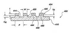
400...편광자410...투명기질400 ... polarizer 410 ... transparent substrate
420...전도성 요소414...첫번째 표면420 ...
430...리브434...영역430
도면을 참고로 본 발명의 다양한 요소는 번호가 매겨질 것이며 당해업자들이 본 발명을 이용해 만들도록 설명될 것이다.Various elements of the present invention will be numbered with reference to the drawings and will be described by those skilled in the art to make using the present invention.
본 발명은 낮은 굴절률 및 제어 두께를 갖는 영역에 의해 지지 기질로부터 분리된 평행한 전도성 요소들의 어레이로 구성된 광대역폭 와이어 그리드 편광자에 관한 것이다. 기질로부터 와이어 그리드를 분리하는 낮은 굴절률 영역은 편광장치에서 두 가지 목적을 위한 역할을 한다. 첫째로, 낮은 굴절률은 가장 긴 파장 공명 포인트를 더 짧은 파장으로 변형시킨다. 두 번째, 낮은 굴절률 영역은 편광자로부터 반사된 P 편광의 성분을 줄일 수 있도록 설계된 제어 두께를 갖는 하나 이상의 층처럼 구현될 수 있다.The present invention relates to a wide-width wire grid polarizer composed of an array of parallel conductive elements separated from a support substrate by regions with low refractive index and control thickness. The low refractive index region separating the wire grid from the substrate serves two purposes in the polarizer. First, the low refractive index transforms the longest wavelength resonance point into a shorter wavelength. Second, the low refractive index region can be implemented like one or more layers with a control thickness designed to reduce the components of P polarized light reflected from the polarizer.
도 4에 도시된 바와 같이, 본 발명에서 와이어 그리드 편광자의 선호되는 실시예를 도시하며 도면부호 400으로 표시된다. 편광자(400)는 투명 기질(410)에 의해 지지되는 복수개의 평행하고 연장된 전도성 요소(420)로 구성된다. 기질(410)은 첫번째 표면(414) 및 굴절률 nS 을 갖는다. 전술된 바와 같이 기질은 유리가 될 수 있고 약 1.5의 굴절률 nS를 가질 수가 있다.As shown in FIG. 4, the preferred embodiment of the wire grid polarizer in the present invention is indicated by
요소들의 크기 및 요소들 배열의 크기는 사용되는 파장에 의해 결정되며, 가시광선의 전체 스펙트럼에 맞춰진다. 요소(420)는 상대적으로 길고 얇다. 선호적으로 각 요소(420)는 가시광선의 파장보다 일반적으로 긴 길이를 갖는다. 그러므로, 요소(420)는 적어도 약 0.7㎛(마이크로미터 혹은 마이크론)의 길이를 갖는다. 그러나 통상적인 길이는 더 길 수 있다.The size of the elements and the size of the array of elements is determined by the wavelength used and fits into the entire spectrum of visible light.
또한 요소(420)는 평행한 배열로 배치되며, 이 요소들의 피치 P(주기나 간격이라고도 함)는 빛의 파장보다 짧다. 그러므로 피치는 0.4㎛(마이크로미터 혹은 마이크론)이하가 될 것이다. 전술된 바와 같이, 정해진 입사각에서 공명을 일으키는 가장 긴 파장을 줄이는 한가지 방법은 주기를 감소시키는 것이다. 그러나 주기를 감소시키는 것은 제작의 어려움을 가져온다. 그러므로 피치 P는 선호적으로 약 빛 파장의 1/2 혹은 0.2㎛이 될 것이다. 또한, 긴 주기(빛 파장의 두배 혹은 1.4㎛보다 큼)를 갖는 그리드는 회절격자 역할을 하고, 짧은 주기(빛의 1/2 파장이나 0.2㎛ 이하)를 갖는 그리드는 편광자로 기능한다. 전이 영역의 주기(약 0.2에서 1.4㎛ 사이)를 가진 그리드는 회절격자 역할을 하며, 공명으로 불리는 변이(anomaly) 혹은 갑작스런 변화로 나타난다. 상기 언급된 바와 같이, 가시 스펙트럼 내에서 공명에 의해 특징지어지는 종래 기술의 장치는 가시 스펙트럼 내의 다양한 파장에서 발생하는 변이에 의해 좁은 작동 범위를 갖는다. 이러한 전이 영역은 와이어 그리드의 작동을 이해하는데 중요한 개념이다. 본 발명의 광대역폭 편광자는 사용될 스펙트럼에 대한 광대역폭 성능을 얻기 위해 전이 영역 밖에 있도록 설계되어야 할 필요가 있다. 그러므로, 전이 영역의 범위는 본 발명의 와이어 그리드 주기에 대한 상단 한계를 정하는데 유용하다.The
설명된 바와 같이, 방정식(1)에 주어진 각도 의존성은 입사각이 커짐에 따라 전이 영역을 긴 파장으로 이동시킨다. 이러한 이동은 피치를 감소시킴으로써 증가될 수 있다. 굴절률 1을 갖는 기질의 법선 입사에서 전이 영역은 약

75°의 각도 및 1.7의 굴절률을 갖는 매우 높은 굴절률을 갖는 유리에 대해서, 방정식(3)은

또한 각 요소(420)는 피치 P에 대해 약 10%에서 90%의 범위가 될 수 있는 폭 W를 갖는다. 요소(420)는 또한 약 200Å 혹은 20nm보다 클 수 있고 제작시 실제적인 제한으로 인해 약 300nm보다 작을 것이다. 또한 요소(420)는 선호적으로 규칙적으로 혹은 동일하게 이격된다.Each
요소의 폭 W는 특정한 적용에 대해 편광자의 성능을 최적화하도록 선택될 수가 있다. 피치에 대한 요소의 폭을 증가시킴으로서, 평행 편광에 대한 반사율이 거의 100%로 증가하며, 직교 편광에 대한 반사율은 0%의 이상적인 값 이상으로 증가시킨다. 그러므로, 피치에 대한 요소 폭의 높은 비율은 투과된 빛에 대해 높은 소광 비율을 제공할 것이다(평행 편광이 투과되지 않기 때문임). 그러나, 반드시 높은 효율이 되는 것은 아니다(왜냐하면 직교 편광 중 일부가 반사될 것이기 때문임). 반대로, 피치에 대한 폭의 낮은 비율은 반사된 광선에 대해서 높은 소광 비율을 제공할 것이지만 고효율이 필수적인 것은 아니다. 평행 광선에 대한 반사율 및 직교 광선에 대한 투과율의 절충에 의해 규정되는 바와 같이 전체 고효율은 피치에 대한 요소의 폭 비율이 40%에서 60%일 때 얻어질 수 있다.The width W of the element can be selected to optimize the performance of the polarizer for a particular application. By increasing the width of the element relative to the pitch, the reflectance for parallel polarized light increases to nearly 100%, and the reflectance for orthogonal polarized light increases above the ideal value of 0%. Therefore, a high ratio of element width to pitch will provide a high extinction ratio for transmitted light (because no parallel polarization is transmitted). However, it is not necessarily high efficiency (because some of the orthogonal polarization will be reflected). Conversely, a low ratio of width to pitch will provide a high extinction ratio for reflected light, but high efficiency is not essential. The overall high efficiency can be obtained when the ratio of the width of the element to the pitch is 40% to 60% as defined by the compromise of the reflectance for parallel light and the transmittance for orthogonal light.
요소(420)의 배열은 축척을 따라 그려진 것이 아니며 이해를 돕기 위해 매우 과장되게 그려졌다. 사실 요소의 배열은 육안으로 관찰될 수 없으며, 매우 높은 배율로 확대하지 않을 경우엔 부분적으로 반사된 표면으로 나타난다. 요소(420)는 금속 같은 광 스펙트럼 거울의 형태로 될 수 있는 재료로 형성된다. 선호적으로 요소의 재료는 가시광선을 이용할 시 은 혹은 알루미늄이다.The arrangement of
선호되는 실시예에서 전도성 요소(420)는 기질(410) 혹은 첫번째 기질(414)로부터 뻗은 리브(430)에 지지된다. 리브(430)는 기질(410)과 동일한 물질일 수 있으며 기질과 일체형으로 형성될 수 있다. 예를 들어, 리브(430)는 하기 설명될 요소(420)를 마스크로 이용하여 요소들(420) 사이에 노출된 기질(410)의 영역을 에칭하여 형성된다.In a preferred embodiment,
리브(430)는 높이 혹은 두께 hR를 가지며, 요소(420)와 기질(410) 사이에, 또는, 요소(420)와, 요소(420)를 기질로부터 분리시키는 표면(414) 사이에 배열되는 영역(434)을 구획한다. 리브(430)에 의해 만들어진 영역(434)은 기질의 굴절률 nS보다 매우 작은 평균 굴절률 nR을 갖는다. 다시 말해서, 리브(434) 및 기질(410)은 nR< nS의 조건을 만족한다. 예를 들어, 리브(430)는 유리가 될 수 있는데 1.525의 굴절률 nS를 갖는다. 동일한 폭의 리브 및 요홈에 대한 유효 매질 굴절률에 대해 브러그맨 방법(Bruggeman's method, Ann. Phy(Leip.), Vol.24, 페이지 636(1935))을 사용하면, nR은 약 1.41의 값을 갖는다.The
영역(434)은 tR로 표시되는 두께를 갖는데, 이 두께는 선호되는 실시예에서 리브(430)의 높이 hR에 의해 정의된다. 요소(420)는 기질(410)로부터 분리되거나 영역의 두께 tR에 동일한 거리에 있는 표면(414)으로부터 분리된다. 리브(430)의 높이 hR 혹은 영역(434)의 두께 tR은 편광자(400)의 성능을 조절하기 위해 변경될 수 있다. 요소(420)를 기질(410) 혹은 표면(414)으로부터 분리하는 것과 기질(410)의 굴절률보다 낮은 굴절률을 갖는 영역(434)을 삽입하는 것은 짧은 파장에서 편광자(410)의 P 편광 투과 효율을 증가시키고, 편광자(410)가 유용한 최소 파장을 낮추며, 또는 가장 높은 공명 포인트를 짧은 파장으로 이동시킨다. 이에 관해 아래에서 자세히 설명될 것이다.
또한 리브(430)는 직사각형 혹은 사각형(440) 형태의 단면을 가질 수도 있고, 사다리꼴(444) 형태의 단면을 가질 수도 있다. 사다리꼴 리브(444)는 리브(444) 사이에 부분적으로 V 형상의 요홈(448)을 형성할 수 있다. 리브(430)의 형상은 또한 편광자(410)의 효율에 영향을 주는데, 하기 자세히 설명될 것이다. 또한 도 4c에 도시된 바와 같이 요소(460)가 리브(462)보다 넓을 수도 있고, 기질(468)의 요홈(464)이 요소(460) 사이의 요홈(470)보다 넓을 수도 있다. 선택적으로 도 4a에 도시된 바와 같이, 요소(480)가 리브(482)보다 더 좁을 수도 있고, 기질(486)의 요홈(484)이 요소(480) 사이의 공간(488)보다 좁을 수도 있다.In addition, the
도 5는 종래 기술에서 0.005, 0.01, 0.04, 0.1㎛인 영역 두께 tR, 혹은 네 개의 다른 리브 높이 hR에 대해 도 4의 편광장치의 P 편광 투과 효율 및 입사광선의 파장 사이의 연산 관계를 나타낸다. 분석의 가정은 이전의 예와 비슷하다: 격자 피치 혹은 주기 p=0.2㎛, 전도체 폭 w=0.1㎛, 전도체 두께 t=0.1㎛, 입사각=45° 기질 굴절률=1.525이다. 선택된 기질 굴절률은 1737 형식 Corning 및 AF45 형식의 Schott을 포함하는 적당한 가격의 박판 유리 재료의 값을 나타낸다. 이러한 분석은 직사각 횡단면의 리브가 전도성 요소 사이의 기질에 이방성 에칭을 하여 형성되는 것을 가정한다.5 is an operational relationship between the prior art at 0.005, 0.01, 0.04, 0.1㎛ in area thickness tR, or four different rib heights P polarized light in the polarization device of Figure 4 forR h and transmission efficiency of the incident light wavelength Indicates. The assumptions of the analysis are similar to the previous examples: lattice pitch or period p = 0.2 μm, conductor width w = 0.1 μm, conductor thickness t = 0.1 μm, incident angle = 45 ° substrate refractive index = 1.525. The substrate refractive index chosen represents the value of a moderately priced thin glass material, including 1737 type Corning and AF45 type Schott. This analysis assumes that the ribs of the rectangular cross section are formed by anisotropic etching on the substrate between the conductive elements.
도 5에 도시된 바와 같이, 0.005와 0.10㎛ 사이의 리브 높이 hR 혹은 영역 두께 tR는 이러한 장치에 유용한 최소 파장을 낮춘다. 0.04 마이크론 높이를 갖는 리브가 존재하면 전체 가시 스펙트럼에 대한 편광장치의 투과효율을 개선시킨다.As shown in FIG. 5, rib height hR or region thickness tR between 0.005 and 0.10 μm. Lowers the minimum wavelength useful for such a device. The presence of ribs with a 0.04 micron height improves the transmission efficiency of the polarizer over the entire visible spectrum.
도 5는 중요한 사실을 나타내는데, 0.005㎛에서 최고 0.1㎛로부터 묘사된 각각의 에칭 깊이는 종래 기술에 대한 본 발명의 성능을 개선시킨다. 0.005㎛만큼 작은 요홈의 깊이가 몰딩된 특정한 와이어 그리드 편광자 구조에 대해 파란색의 짧은 파장에서의 성능에 얼마나 중요한 영향을 주는지 주목할 만 하다. 이 결과는 짧은 주기에서 효과가 좀더 뚜렷해지는 초기 실험뿐만 아니라 많은 비슷한 연산에서도 관찰되었다. 1nm에서 2nm만큼 작은 높이를 갖는 리브조차 몇가지 특정한 와이어 그리드 편광자 구조에 대해 중요하다.5 shows an important fact: each etch depth depicted from 0.005 μm up to 0.1 μm improves the performance of the present invention over the prior art. It is noteworthy how important the depth of the groove, as small as 0.005 μm, has an important effect on performance at short wavelengths of blue for certain wire grid polarizer structures molded. This result has been observed in many similar operations as well as in the initial experiments where the effect becomes more pronounced in short cycles. Even ribs with heights as small as 1 nm to 2 nm are important for some specific wire grid polarizer structures.
리브의 정확한 형상은 편광자의 성능에 부가적인 영향을 갖는다. 도 5는 편광자에 대해 파장 및 P 편광 투과 효율 사이의 연산관계를 나타내는데, 전도성 요소는 기질에 에칭된 V 형상의 요홈에 의해 분리된 사다리꼴 리브에 지지된다. 사다리꼴 리브의 효과 역시 비슷하지만, 전술된 직사각 리브의 것만큼 이점이 있지는 않는다.The exact shape of the ribs has an additional effect on the performance of the polarizer. Figure 5 shows the arithmetic relationship between wavelength and P polarization transmission efficiency for the polarizer, wherein the conductive element is supported by trapezoidal ribs separated by V-shaped grooves etched into the substrate. The effect of the trapezoidal ribs is similar, but not as advantageous as that of the rectangular ribs described above.
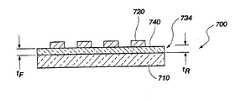
도 7은 본 발명의 선택적인 실시예에 대한 횡단 다이어그램을 나타낸다. 편광자(700)은 투명 기질(710)에 의해 지지되는 복수개의 평행, 연장 전도성 요소(720)들로 구성된다. 절연 재료로 된 하나 이상의 층 혹은 필름(740)이 전도성 요소(720)와 기질(710)에 삽입된다. 층 혹은 필름(740)은 두께 tF, 굴절률 nF를 갖으며, 영역 두께 tR을 갖는 영역(734)을 정의한다. 공명 포인트를 짧은 파장으로 변형시키는 요망 효과를 얻기 위해서, 절연 층(740) 중 적어도 하나는 기질(710)의 굴절률 nS보다 작은 굴절률 nF를 가져야 한다. 즉, 조건 nF<nS를 만족시켜야 한다.7 shows a cross-sectional diagram for an alternative embodiment of the present invention.
도 8은 종래의 기술에 비해, 0.04, 0.1, 0.22㎛인 세가지 두께 tF를 갖는 마그네슘 플루오르화물(MgF2)(n=1.38)의 단일층이 기질과 전도성 요소 사이에 삽입될 때, 와이어 그리드 편광자에 대한 P 편광 투과 효율 및 파장 사이의 연산관계를 나타낸다. 이러한 분석의 그외 다른 가정은 이전의 예와 동일하다. MgF2의 두께를 0에서 0.22㎛로 증가시키는 것은 가장 긴 파장 공명 포인트를 0.445에서 0.41㎛로 변형시키므로, 편광장치의 유용한 대역폭을 증가시킨다. 0.22 마이크론 필름이 존재하면 전체 가시 스펙트럼에 대한 편광자 투과율이 개선된다.FIG. 8 shows a wire grid polarizer when a single layer of magnesium fluoride (MgF2 ) (n = 1.38) having three thicknesses tF of 0.04, 0.1, 0.22 μm compared to the prior art is inserted between the substrate and the conductive element. The arithmetic relationship between P polarization transmission efficiency and wavelength for. Other assumptions of this analysis are the same as in the previous example. Increasing the thickness of MgF2 from 0 to 0.22 μm transforms the longest wavelength resonance point from 0.445 to 0.41 μm, thus increasing the useful bandwidth of the polarizer. The presence of 0.22 micron film improves polarizer transmission over the entire visible spectrum.
오톤(Auton, Applied Optics, Volume 6 no.6, 1967년 6월, 페이지 1023-7)은 와이어 그리드와 지지 기질 사이의 "블루밍 레이어(blooming layer)"라고 하는 단일 층 반사방지 코팅 사용에 관해 공지하였다. 단순한 임피던스-매칭(impedance matching) 공식 및 박판 금속 스트립을 완벽하게 전도하는 것을 기초로 하는 그의 분석에서, 이 층은 기질의 굴절률의 제곱근에 해당하는 굴절률과, 파장의 1/4에 해당하는 광학 두께를 가져야 한다. 오톤은 이러한 방법으로 제조된 와이어 그리드의 성능은 "단일 파장만이 요구되는 레이저 장비"에 대해 지지되지 않는 그리드의 성능과 동일하다는 결론을 내렸다. 오톤은 그리드 간격이 파장보다 훨씬 짧다는 가정때문에 공명 효과를 무시하였으며, 이러한 공명 효과에 대해서 알지도 못하고 있었다. 또한, 블루밍 레이어에 대한 조건은 방정식(1)에 의해 예상된 바와 같이 공명을 억제하거나 이동시키기 위해 필요한 조건과는 다르다. 오톤에 의해 제시된 임피던스-매칭 블루밍 레이어는 좁은 범위의 매개변수에 대해 효율적이지만 본 발명의 실시예는 넓은 범위의 매개변수에 대해 효율적일 것이다. 그러므로 오톤은 본 발명의 두 번째 실시예를 제시하지 못했다.Othon (Auton, Applied Optics, Volume 6 no.6, June 1967, page 1023-7) announces the use of a single layer antireflective coating called the "blooming layer" between the wire grid and the support substrate. It was. In its analysis, which is based on a simple impedance-matching formula and perfect conduction of thin metal strips, this layer has a refractive index corresponding to the square root of the refractive index of the substrate and an optical thickness corresponding to 1/4 of the wavelength. Should have Othon concluded that the performance of wire grids manufactured in this way is equivalent to the performance of grids not supported for "laser equipment requiring only a single wavelength." Orton ignored the resonance effect because of the assumption that the grid spacing was much shorter than the wavelength, and he did not know about it. Also, the conditions for the blooming layer are different from the conditions necessary for suppressing or shifting the resonance as expected by equation (1). The impedance-matching blooming layer presented by Otone is efficient for a narrow range of parameters, but embodiments of the present invention will be efficient for a wide range of parameters. Otone therefore did not present a second embodiment of the present invention.
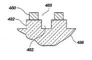
도 9는 편광 장치(900)가, 리브(940)에 의해 지지되는 전도성 요소(920)로 구성된 본 발명의 또 다른 실시예의 횡단면도이다. 리브(940)는 하나 이상의 절연 층(944)에 에칭하여 형성될 수 있고 전도성 요소(920) 사이에 노출된 기질(910)까지 에칭하여 형성될 수도 있다. 그러므로 리브(940)는 하나 이상의 필름 층(944)에 의해 형성될 수도 있고, 그 일부분에 의해 형성될 수도 있다(도면부호 950, 960으로 표시됨). 또한 리브(940)는 다중 필름 층(944)에 의해 형성될 수 있다. 필름 층(944)은 단일 재료의 필요한 높이 혹은 두께를 달성하는 동일한 재료의 다중 층이 될 수 있다. 필름 층(944)은 또한 다른 효과 혹은 성능 특성을 이루기 위해 다양한 다른 재료가 될 수 있다.9 is a cross-sectional view of another embodiment of the present invention in which the
또한 리브(940)는 여러 다른 물질들의 층(970)으로 형성될 수 있다. 층(970)들 중 하나는 기질(910)과 동일한 재료가 될 수 있고, 기질(910)과 일체형으로 형성될 수 있다. 예를 들어, 층(970)들 중 하나는 도 4에 도시된 리브(430)와 비슷할 수 있고, 전체 리브(940)의 영역을 형성하는 부분 기질 리브(948)를 정의한다. 그러므로, 리브(940)는 필름 층(944)에 의해, 그리고 기질(910)에 형성된 기질 리브(948)에 의해 형성될 수 있고, 이때, 필름층(944)이 기질 리브(948)에 증착된다. 상기 표시된 바와 같이, 리브(940)는 요소(920)들 사이에서 층(944)과 기질(910)에 에칭하여 형성된다.
필름층(944)에 형성될 수 있는 리브(940)에 의해, 필름층(944)에 의해, 또는, 필름 층(944) 및 기질 리브(948)에 의해 영역(934)이 형성될 수 있다. 이러한 구성은 낮은 굴절률 층의 효과 및 리브된 기질의 효과를 결합할 수 있는 잠재력을 갖는다. 리브(940)의 전체 높이 hR는 (950)에 나타낸 바와 같이 절연 층(944) 두께 tF의 일부분일 수도 있고, (960)에 나타낸 것 같이 절연 층(944) 두께 tF와 동일할 수도 있고, (970)에 나타난 것 같이 절연 층(944) 두께 tF를 넘을 수도 있다. 그러므로 (970)에 나타난 바와 같이, 영역 두께 tR과 전체 리브(940)의 높이 hR은 층(944) 두께 tF 및 기질 리브(948) 높이 hS에 의해 형성된다. 기질 리브(948)는 기질 리브(948) 및 필름 층(944)에 의해 형성된 조합 리브(940) 구조가 되며, 각각의 기질 리브(948)에는 복수개의 필름 층(944)이 형성된다.
도 10은 편광 장치에 대한 파장과 P-편광 투과율 사이의 관계를 도시하는데, 이 편광장치는 기질과 전도성 요소 사이에 MgF2 단일 층을 가지며, 기질 리브 높이 hS 및 MgF2 필름 두께 tF에 관한 세가지 종류의 조합으로 만들어진다. 두가지 경우엔 기질 리브 높이 hS 및 MgF2 필름 두께 tF가 동일하다. 첫 번째의 경우, 기질 리브 높이 hS 및 필름 두께 tF는 0.08㎛의 영역 두께 tR 및 리브 높이 hR에 대해 0.04㎛로 동일하다. 두 번째의 경우, 기질 리브 높이 hS 및 필름 두께 tF는 0.2㎛의 리브 높이 hR 및 영역 두께 tR에 대해 0.1㎛으로 동일하다. 세 번째의 경우, 0.26㎛의 영역 두께 tR에 대해 MgF2 필름 두께 tF는 0.22㎛이고 기질 리브 높이 hS는 0.04㎛이다. 종래의 편광자에 비교해 볼 때, 세 번째 조합은 50% 투과율 지점을 0.46㎛에서 약 0.41㎛로 변형시키며, 가시 스펙트럼에 대해 평균 편광자 투과율을 약 6%정도 증가시킨다.FIG. 10 shows the relationship between wavelength and P-polarization transmittance for a polarizer, which has a single layer of MgF2 between the substrate and the conductive element, at substrate rib height hS and MgF2 film thickness tF. It is made of a combination of three kinds In both cases the substrate rib height hS and the MgF2 film thickness tF are the same. In the first case, the substrate rib height hS and the film thickness tF are the same at 0.04 μm for the area thickness tR and rib height hR of 0.08 μm. In the second case, the substrate rib height hS and the film thickness tF are equal to 0.1 μm for the rib height hR and the region thickness tR of 0.2 μm. In the third case, the MgF2 film thickness tF is 0.22 μm and the substrate rib height hS is 0.04 μm for an area thickness tR of 0.26 μm. Compared to conventional polarizers, the third combination transforms the 50% transmittance point from 0.46 μm to about 0.41 μm and increases the average polarizer transmittance by about 6% over the visible spectrum.
도 11은 도 4에 도시된 바와 같이 편광 장치를 제조하는 과정을 도시한다. 첫 번째 단계는 기질(1110) 위에 평행 전도성 요소(1120)들의 어레이를 형성하는 것이다. 이러한 요소(1120)의 형성은 몇가지 종래의 과정으로 이루어질 수 있다. 예를 들어,가빈(Garvin)의 미국 특허 제 4,049,944 호와, 페란트(Ferrante)의 미국 특허 제 4,514,479 호에서는 홀로그래픽 간섭 리소리그래피를 이용하여 포토레지스트에 정밀 격자 구조를 형성하고, 이온 빔 메칭을 실시하여 이 정밀 격자 구조를 기초 금속 필름에 전이하는 방법을 제시하고 있다. 스텐캄프(Stenkamp, "가시 스펙트럼 영역에 대한 그리드 편광자", Proceedings of the SPIE, vol.2213, 페이지 288-296))는 직접 전자-광선(e-beam) 리소그래피를 이용하여 레지스트 패턴을 생성하고, 이어서, 반응성 이온 에칭을 통해 이 패턴을 금속 필름에 전이하는 기술을 제시하고 있다. 극자외선 리소그래피 및 X-레이 리소그래피를 포함한 그외 다른 고해상도 리소그래피 기술이 레지스트 패턴을 만들기 위해 사용될 수 있다. 다른 에칭 메카니즘 및 리프트-오프(lift-off) 처리를 포함한 그외 다른 기술들이 레지스트로부터 금속 필름까지 패턴을 전이하는 데 사용될 수 있다. 팽행 전도성 요소 어레이를 형성하기 위해 사용된 정확한 프로세스는 본 발명에서 중요하지 않다.FIG. 11 illustrates a process of manufacturing a polarizer as shown in FIG. 4. The first step is to form an array of parallel
평행 전도성 요소(1120)가 형성된 후인 두 번째 단계는 전도성 요소(1120)를 마스크처럼 이용하여 기질(1110)을 에칭하고, 이어서, 전도체(1120)를 지지하는 리브(1130)을 만드는 것이다. 적합한 화학물의 반응 이온 에칭 혹은 이온 광선 에칭이 사용되어 기질(1110)의 재료에 따라 기질(1110)에 요홈을 에칭할 수 있다.The second step, after the parallel
도 12는 도 7 및 도 9에 도시된 편광장치를 제조하기 위한 처리과정을 도시한다. 첫 번째 단계는 하나의 투명 기질(1210)의 표면 위에 여러개의 투명 절연필름 층(1230)을 적층시키는 것이다. 두 번째 단계는 전술된 바와 같이 평행 전도성 요소(1220)의 어레이를 형성하는 것이다. 세 번째 단계는 전도성 요소(1220)를 마스크로 이용하여 기초 층(1230)을 에칭하여 전도성 요소를 지지할 리브(1240)를 형성하는 것이다. 에칭의 깊이는 얇은 절연 필름 층(1230) 두께로 제한될 수 있고, 절연 필름 층(1230)을 통해 연장될 수 있거나 혹은 절연 필름 층(1230)을 통해 기질(1210) 안으로 뻗을 수도 있다.
본 발명의 선호되는 실시예에 따르면, 요소의 주기는 가시광선 파장의 1/2 내지 2배에 해당한다. 또한가지 실시예에서는 요소의 주기가 가시광선 파장의 0.19 내지 0.5에 해당한다.
본 발명의 선호 실시예에 따르면, 요소의 주기는 0.076 내지 1.4㎛에 해당하며, 0.076 내지 0.2㎛이 더욱 선호된다.
본 발명의 선호 실시예에 따르면, 영역의 두께가 0.001 내지 0.3㎛에 해당한다.
본 발명의 선호 실시예에 따르면, 요소의 두께는 0.04 내지 0.3㎛에 해당한다. 요소의 재료로는 알루미늄이나 은이 선호된다.
본 발명의 선호 실시예에 따르면, 마그네슘플루오르화물과 같은 리브를 구성하는 한개 이상의 물질층의 두께는 0.04 내지 0.22 미크론에 해당한다.
본 발명의 선호 실시예에 따르면, 영역을 구성하는 절연 물질층의 두께는 0.001 내지 0.3 미크론에 해당한다.FIG. 12 shows a process for manufacturing the polarizer shown in FIGS. 7 and 9. The first step is to deposit several transparent insulating film layers 1230 on the surface of one
According to a preferred embodiment of the present invention, the period of the element corresponds to 1/2 to 2 times the visible light wavelength. In another embodiment, the period of the element corresponds to 0.19 to 0.5 of the visible light wavelength.
According to a preferred embodiment of the present invention, the period of the element corresponds to 0.076 to 1.4 μm, more preferably 0.076 to 0.2 μm.
According to a preferred embodiment of the present invention, the thickness of the region corresponds to 0.001 to 0.3 mu m.
According to a preferred embodiment of the present invention, the thickness of the element corresponds to 0.04 to 0.3 μm. As the material of the element, aluminum or silver is preferred.
According to a preferred embodiment of the present invention, the thickness of at least one material layer constituting the rib, such as magnesium fluoride, corresponds to 0.04 to 0.22 microns.
According to a preferred embodiment of the present invention, the thickness of the insulating material layer constituting the region corresponds to 0.001 to 0.3 micron.
본 발명의 전술된 실시예는 설명을 위한 것이며, 당해업자에 의해 변형이 가능하다. 예를 들어, 본 발명에서 입사각이 45도인 것으로 예를 들었지만, 편광장치의 물리적 매개변수를 적합하게 조절하여 다른 입사각으로 동일하게 적용될 수가 있다. 또한 본 발명의 주요 이점이 편광장치의 유용한 대역폭을 가시 스펙트럼의 짧은 파장 범위로 확장시키는 것이지만, 적외선처럼 스펙트럼의 다른 영역에서 사용되는 편광장치의 투과율을 개선시키기 위해 사용될 수도 있다. 본 발명에 따라 당해업자들에 의해 다양한 설계와 변형이 이루어질 수 있다. 또한 본 발명의 전술된 실시예에만 국한되지는 않지만, 청구항에 의해 형성되는 부분에는 제한된다.The above-described embodiment of the present invention is for the purpose of illustration, and may be modified by those skilled in the art. For example, although the incidence angle is 45 degrees in the present invention, it may be equally applied to other incidence angles by appropriately adjusting the physical parameters of the polarizer. The main advantage of the present invention is also to extend the useful bandwidth of the polarizer to the short wavelength range of the visible spectrum, but may also be used to improve the transmittance of polarizers used in other regions of the spectrum, such as infrared. Various designs and modifications may be made by those skilled in the art in accordance with the present invention. It is also not limited to the foregoing embodiments of the invention, but is limited to the parts formed by the claims.
Claims (96)
Translated fromKorean

Applications Claiming Priority (2)
| Application Number | Priority Date | Filing Date | Title |
|---|---|---|---|
| US09/337,970 | 1999-06-22 | ||
| US09/337,970US6122103A (en) | 1999-06-22 | 1999-06-22 | Broadband wire grid polarizer for the visible spectrum |
Publications (2)
| Publication Number | Publication Date |
|---|---|
| KR20020021129A KR20020021129A (en) | 2002-03-18 |
| KR100714531B1true KR100714531B1 (en) | 2007-05-07 |
Family
ID=23322826
Family Applications (1)
| Application Number | Title | Priority Date | Filing Date |
|---|---|---|---|
| KR1020017016236AExpired - Fee RelatedKR100714531B1 (en) | 1999-06-22 | 2000-06-22 | Broadband Wire Grid Polarizers for the Visible Spectrum |
Country Status (11)
| Country | Link |
|---|---|
| US (1) | US6122103A (en) |
| EP (1) | EP1192486B1 (en) |
| JP (4) | JP2003502708A (en) |
| KR (1) | KR100714531B1 (en) |
| CN (1) | CN1231772C (en) |
| AU (1) | AU769457B2 (en) |
| BR (1) | BR0012529A (en) |
| CA (1) | CA2375522A1 (en) |
| HK (1) | HK1047977B (en) |
| TW (1) | TW546494B (en) |
| WO (1) | WO2000079317A1 (en) |
Cited By (1)
| Publication number | Priority date | Publication date | Assignee | Title |
|---|---|---|---|---|
| KR101131101B1 (en) | 2008-12-18 | 2012-04-03 | 주식회사 엘지화학 | Method for manufacturing of reflective type polarizer |
Families Citing this family (367)
| Publication number | Priority date | Publication date | Assignee | Title |
|---|---|---|---|---|
| US6563582B1 (en)* | 1998-10-07 | 2003-05-13 | Cornell Seu Lun Chun | Achromatic retarder array for polarization imaging |
| US7306338B2 (en) | 1999-07-28 | 2007-12-11 | Moxtek, Inc | Image projection system with a polarizing beam splitter |
| US6447120B2 (en) | 1999-07-28 | 2002-09-10 | Moxtex | Image projection system with a polarizing beam splitter |
| US6666556B2 (en) | 1999-07-28 | 2003-12-23 | Moxtek, Inc | Image projection system with a polarizing beam splitter |
| US6542307B2 (en) | 2000-10-20 | 2003-04-01 | Three-Five Systems, Inc. | Compact near-eye illumination system |
| US6563648B2 (en) | 2000-10-20 | 2003-05-13 | Three-Five Systems, Inc. | Compact wide field of view imaging system |
| US7849198B2 (en)* | 2000-10-24 | 2010-12-07 | Litepoint Corporation | System, method and article of manufacture for utilizing an interface client in an interface roaming network framework |
| US7352424B2 (en) | 2000-11-17 | 2008-04-01 | Deep Video Imaging Limited | Altering surface of display screen from matt to optically smooth |
| JP2002182003A (en)* | 2000-12-14 | 2002-06-26 | Canon Inc | Anti-reflection function element, optical element, optical system and optical equipment |
| AU2002241632A1 (en)* | 2000-12-27 | 2002-07-08 | Technion Research And Development Foundation Ltd. | Space-variant subwavelength polarization grating and applications thereof |
| US6532111B2 (en)* | 2001-03-05 | 2003-03-11 | Eastman Kodak Company | Wire grid polarizer |
| GB0106050D0 (en)* | 2001-03-12 | 2001-05-02 | Suisse Electronique Microtech | Polarisers and mass-production method and apparatus for polarisers |
| US6585378B2 (en) | 2001-03-20 | 2003-07-01 | Eastman Kodak Company | Digital cinema projector |
| US7375887B2 (en) | 2001-03-27 | 2008-05-20 | Moxtek, Inc. | Method and apparatus for correcting a visible light beam using a wire-grid polarizer |
| JP2003215344A (en)* | 2001-03-29 | 2003-07-30 | Seiko Epson Corp | Polarizer and optical device using the polarizer |
| AU2002248784A1 (en) | 2001-04-20 | 2002-11-05 | Corning Precision Lens Incorporated | Methods and apparatus for positioning optical prisms |
| NZ511255A (en) | 2001-04-20 | 2003-12-19 | Deep Video Imaging Ltd | Multi-focal plane display having an optical retarder and a diffuser interposed between its screens |
| WO2002095487A1 (en) | 2001-05-18 | 2002-11-28 | 3M Innovative Properties Company | Polarization arrangement |
| US6784991B2 (en)* | 2001-06-18 | 2004-08-31 | Therma-Wave, Inc. | Diffractive optical elements and grid polarizers in focusing spectroscopic ellipsometers |
| WO2003032029A1 (en)* | 2001-10-09 | 2003-04-17 | Koninklijke Philips Electronics N.V. | Optical devices |
| NZ514500A (en) | 2001-10-11 | 2004-06-25 | Deep Video Imaging Ltd | A multiplane visual display unit with a transparent emissive layer disposed between two display planes |
| US6714350B2 (en) | 2001-10-15 | 2004-03-30 | Eastman Kodak Company | Double sided wire grid polarizer |
| US6739723B1 (en) | 2001-12-07 | 2004-05-25 | Delta Electronics, Inc. | Polarization recapture system for liquid crystal-based data projectors |
| EP1461962A1 (en)* | 2002-01-07 | 2004-09-29 | 3M Innovative Properties Company | Color component aperture stops in projection display system |
| US6909473B2 (en) | 2002-01-07 | 2005-06-21 | Eastman Kodak Company | Display apparatus and method |
| US7061561B2 (en) | 2002-01-07 | 2006-06-13 | Moxtek, Inc. | System for creating a patterned polarization compensator |
| US6884500B2 (en)* | 2002-02-12 | 2005-04-26 | Unaxis Balzers Ltd. | Component comprising submicron hollow spaces |
| US6590695B1 (en) | 2002-02-26 | 2003-07-08 | Eastman Kodak Company | Micro-mechanical polarization-based modulator |
| EP1478965A1 (en)* | 2002-02-28 | 2004-11-24 | 3M Innovative Properties Company | Compound polarization beam splitters |
| US7742239B2 (en) | 2002-03-17 | 2010-06-22 | Puredepth Limited | Method to control point spread function of an image |
| US6785050B2 (en) | 2002-05-09 | 2004-08-31 | Moxtek, Inc. | Corrosion resistant wire-grid polarizer and method of fabrication |
| US6648475B1 (en) | 2002-05-20 | 2003-11-18 | Eastman Kodak Company | Method and apparatus for increasing color gamut of a display |
| US6876784B2 (en)* | 2002-05-30 | 2005-04-05 | Nanoopto Corporation | Optical polarization beam combiner/splitter |
| US6805445B2 (en) | 2002-06-05 | 2004-10-19 | Eastman Kodak Company | Projection display using a wire grid polarization beamsplitter with compensator |
| US7131737B2 (en)* | 2002-06-05 | 2006-11-07 | Moxtek, Inc. | Housing for mounting a beamsplitter and a spatial light modulator with an output optical path |
| US7283571B2 (en)* | 2002-06-17 | 2007-10-16 | Jian Wang | Method and system for performing wavelength locking of an optical transmission source |
| US7386205B2 (en)* | 2002-06-17 | 2008-06-10 | Jian Wang | Optical device and method for making same |
| EP1520203A4 (en) | 2002-06-18 | 2005-08-24 | Nanoopto Corp | Optical components exhibiting enhanced functionality and method of making same |
| JP2004045672A (en)* | 2002-07-11 | 2004-02-12 | Canon Inc | Polarization separation element and optical system using the same |
| AU2003281120B2 (en) | 2002-07-15 | 2010-05-20 | Puredepth Limited | Improved multilayer video screen |
| AU2003257961A1 (en) | 2002-08-01 | 2004-02-23 | Nanoopto Corporation | Precision phase retardation devices and method of making same |
| US20040032663A1 (en)* | 2002-08-19 | 2004-02-19 | Tekolste Robert | Wafer level polarization control elements |
| CN1682132A (en)* | 2002-08-21 | 2005-10-12 | 纳诺普托公司 | Method and system for providing beam polarization |
| US6809873B2 (en)* | 2002-09-09 | 2004-10-26 | Eastman Kodak Company | Color illumination system for spatial light modulators using multiple double telecentric relays |
| US7190521B2 (en)* | 2002-09-13 | 2007-03-13 | Technion Research And Development Foundation Ltd. | Space-variant subwavelength dielectric grating and applications thereof |
| NZ521505A (en) | 2002-09-20 | 2005-05-27 | Deep Video Imaging Ltd | Multi-view display |
| US7013064B2 (en) | 2002-10-09 | 2006-03-14 | Nanoopto Corporation | Freespace tunable optoelectronic device and method |
| US6920272B2 (en)* | 2002-10-09 | 2005-07-19 | Nanoopto Corporation | Monolithic tunable lasers and reflectors |
| US6850329B2 (en)* | 2002-10-15 | 2005-02-01 | Mitutoyo Corporation | Interferometer using integrated imaging array and high-density polarizer array |
| US6665119B1 (en) | 2002-10-15 | 2003-12-16 | Eastman Kodak Company | Wire grid polarizer |
| US7264390B2 (en)* | 2002-10-23 | 2007-09-04 | Hannstar Display Corp. | Polarized light source device and back light module for liquid crystal display |
| DE10260819A1 (en)* | 2002-12-23 | 2004-07-01 | Carl Zeiss Smt Ag | Method for producing micro-structured optical elements involves provision of an auxiliary layer with a surface structure, and transfer of this structure unaltered to a substrate |
| US7113335B2 (en)* | 2002-12-30 | 2006-09-26 | Sales Tasso R | Grid polarizer with suppressed reflectivity |
| US7008065B2 (en) | 2003-01-07 | 2006-03-07 | 3M Innovative Properties Company | Color component aperture stops in projection display system |
| US20040150794A1 (en)* | 2003-01-30 | 2004-08-05 | Eastman Kodak Company | Projector with camcorder defeat |
| EP1597616A4 (en)* | 2003-02-10 | 2008-04-09 | Nanoopto Corp | Universal broadband polarizer, devices incorporating same, and method of making same |
| US7206059B2 (en)* | 2003-02-27 | 2007-04-17 | Asml Netherlands B.V. | Stationary and dynamic radial transverse electric polarizer for high numerical aperture systems |
| US6943941B2 (en)* | 2003-02-27 | 2005-09-13 | Asml Netherlands B.V. | Stationary and dynamic radial transverse electric polarizer for high numerical aperture systems |
| US20040174596A1 (en)* | 2003-03-05 | 2004-09-09 | Ricoh Optical Industries Co., Ltd. | Polarization optical device and manufacturing method therefor |
| US7098442B2 (en)* | 2003-03-05 | 2006-08-29 | Raytheon Company | Thin micropolarizing filter, and a method for making it |
| US6758565B1 (en)* | 2003-03-20 | 2004-07-06 | Eastman Kodak Company | Projection apparatus using telecentric optics |
| WO2004085670A2 (en)* | 2003-03-24 | 2004-10-07 | Perkinelmer Las, Inc. | Polarization detection |
| KR20040086029A (en)* | 2003-03-27 | 2004-10-08 | 삼성전자주식회사 | High efficiency projection system |
| US7221759B2 (en)* | 2003-03-27 | 2007-05-22 | Eastman Kodak Company | Projector with enhanced security camcorder defeat |
| NL1025813C2 (en)* | 2003-03-27 | 2006-01-17 | Samsung Electronics Co Ltd | Image projection system, has polarization conversion system transmitting one polarized beam from incident light and reflecting another polarized beam toward incidence plane, and projection lens unit magnifying color picture |
| KR100619006B1 (en)* | 2003-03-28 | 2006-08-31 | 삼성전자주식회사 | High efficiency projection system |
| NL1025731C2 (en)* | 2003-03-28 | 2006-01-10 | Samsung Electronics Co Ltd | Highly efficient projection system for providing a picture to a large screen has polarization conversion system set between the color separator and light valve, and which converts incident beam into beam with single polarization |
| US20040259279A1 (en)* | 2003-04-15 | 2004-12-23 | Erchak Alexei A. | Light emitting device methods |
| US7083993B2 (en)* | 2003-04-15 | 2006-08-01 | Luminus Devices, Inc. | Methods of making multi-layer light emitting devices |
| US7074631B2 (en)* | 2003-04-15 | 2006-07-11 | Luminus Devices, Inc. | Light emitting device methods |
| US7105861B2 (en)* | 2003-04-15 | 2006-09-12 | Luminus Devices, Inc. | Electronic device contact structures |
| US7274043B2 (en)* | 2003-04-15 | 2007-09-25 | Luminus Devices, Inc. | Light emitting diode systems |
| US7262550B2 (en)* | 2003-04-15 | 2007-08-28 | Luminus Devices, Inc. | Light emitting diode utilizing a physical pattern |
| US6831302B2 (en)* | 2003-04-15 | 2004-12-14 | Luminus Devices, Inc. | Light emitting devices with improved extraction efficiency |
| US7084434B2 (en)* | 2003-04-15 | 2006-08-01 | Luminus Devices, Inc. | Uniform color phosphor-coated light-emitting diode |
| US7098589B2 (en) | 2003-04-15 | 2006-08-29 | Luminus Devices, Inc. | Light emitting devices with high light collimation |
| US7166871B2 (en)* | 2003-04-15 | 2007-01-23 | Luminus Devices, Inc. | Light emitting systems |
| US7667238B2 (en)* | 2003-04-15 | 2010-02-23 | Luminus Devices, Inc. | Light emitting devices for liquid crystal displays |
| US7521854B2 (en)* | 2003-04-15 | 2009-04-21 | Luminus Devices, Inc. | Patterned light emitting devices and extraction efficiencies related to the same |
| US7211831B2 (en)* | 2003-04-15 | 2007-05-01 | Luminus Devices, Inc. | Light emitting device with patterned surfaces |
| US6738127B1 (en)* | 2003-04-24 | 2004-05-18 | Eastman Kodak Company | LCD-based printing apparatus for printing onto high contrast photosensitive medium |
| US20040258355A1 (en)* | 2003-06-17 | 2004-12-23 | Jian Wang | Micro-structure induced birefringent waveguiding devices and methods of making same |
| JP4425059B2 (en) | 2003-06-25 | 2010-03-03 | シャープ株式会社 | Polarizing optical element and display device using the same |
| US6769779B1 (en) | 2003-07-22 | 2004-08-03 | Eastman Kodak Company | Housing for mounting modulation and polarization components in alignment with an optical path |
| US6847057B1 (en) | 2003-08-01 | 2005-01-25 | Lumileds Lighting U.S., Llc | Semiconductor light emitting devices |
| US6992778B2 (en)* | 2003-08-08 | 2006-01-31 | Mitutoyo Corporation | Method and apparatus for self-calibration of a tunable-source phase shifting interferometer |
| US7230717B2 (en)* | 2003-08-28 | 2007-06-12 | 4D Technology Corporation | Pixelated phase-mask interferometer |
| US7057737B2 (en)* | 2003-08-29 | 2006-06-06 | 4D Technology Corporation | Common optical-path testing of high-numerical-aperture wavefronts |
| US7341880B2 (en)* | 2003-09-17 | 2008-03-11 | Luminus Devices, Inc. | Light emitting device processes |
| US7344903B2 (en)* | 2003-09-17 | 2008-03-18 | Luminus Devices, Inc. | Light emitting device processes |
| TWI223103B (en)* | 2003-10-23 | 2004-11-01 | Ind Tech Res Inst | Wire grid polarizer with double metal layers |
| CN1621866A (en)* | 2003-11-28 | 2005-06-01 | 日本板硝子株式会社 | Thin-film structure and method for producing the same |
| JP2005172844A (en)* | 2003-12-05 | 2005-06-30 | Enplas Corp | Wire grid polarizer |
| US7450311B2 (en) | 2003-12-12 | 2008-11-11 | Luminus Devices, Inc. | Optical display systems and methods |
| CN1316265C (en)* | 2003-12-16 | 2007-05-16 | 财团法人工业技术研究院 | Polarizing component with double metal layer grating and manufacturing method thereof |
| US6902277B1 (en) | 2004-01-06 | 2005-06-07 | Eastman Kodak Company | Housing for a spatial light modulator |
| US6863400B1 (en) | 2004-01-21 | 2005-03-08 | Eastman Kodak Company | Tiled projection display using spatial light modulators |
| JP2005242080A (en)* | 2004-02-27 | 2005-09-08 | Victor Co Of Japan Ltd | Wire grid polarizer |
| US7408201B2 (en)* | 2004-03-19 | 2008-08-05 | Philips Lumileds Lighting Company, Llc | Polarized semiconductor light emitting device |
| US7808011B2 (en)* | 2004-03-19 | 2010-10-05 | Koninklijke Philips Electronics N.V. | Semiconductor light emitting devices including in-plane light emitting layers |
| US7304719B2 (en)* | 2004-03-31 | 2007-12-04 | Asml Holding N.V. | Patterned grid element polarizer |
| US7670758B2 (en)* | 2004-04-15 | 2010-03-02 | Api Nanofabrication And Research Corporation | Optical films and methods of making the same |
| US20050275944A1 (en) | 2004-06-11 | 2005-12-15 | Wang Jian J | Optical films and methods of making the same |
| US7997771B2 (en) | 2004-06-01 | 2011-08-16 | 3M Innovative Properties Company | LED array systems |
| US7413317B2 (en)* | 2004-06-02 | 2008-08-19 | 3M Innovative Properties Company | Polarized UV exposure system |
| WO2006004010A1 (en)* | 2004-06-30 | 2006-01-12 | Zeon Corporation | Electromagnetic wave shielding grid polarizer and its manufacturing method and grid polarizer manufacturing method |
| US20060001969A1 (en)* | 2004-07-02 | 2006-01-05 | Nanoopto Corporation | Gratings, related optical devices and systems, and methods of making such gratings |
| TWI266117B (en)* | 2004-07-06 | 2006-11-11 | Au Optronics Corp | Backlight module capable of polarized light interchange |
| US20090023239A1 (en)* | 2004-07-22 | 2009-01-22 | Luminus Devices, Inc. | Light emitting device processes |
| KR100483352B1 (en)* | 2004-07-27 | 2005-04-14 | (주)파버나인 | Liquid crystal display device using thin film polarizers and retarders |
| US20060038188A1 (en)* | 2004-08-20 | 2006-02-23 | Erchak Alexei A | Light emitting diode systems |
| JP4389791B2 (en)* | 2004-08-25 | 2009-12-24 | セイコーエプソン株式会社 | Fine structure manufacturing method and exposure apparatus |
| KR20060022135A (en)* | 2004-09-06 | 2006-03-09 | 주식회사 하이닉스반도체 | Polarized reticle |
| US7476910B2 (en)* | 2004-09-10 | 2009-01-13 | Kabushiki Kaisha Toshiba | Semiconductor light emitting device and method for manufacturing the same |
| EP1635199A1 (en)* | 2004-09-14 | 2006-03-15 | LG Electronics Inc. | Wire grid polarizer and manufacturing method thereof |
| US20060056024A1 (en)* | 2004-09-15 | 2006-03-16 | Ahn Seh W | Wire grid polarizer and manufacturing method thereof |
| US7480017B2 (en)* | 2004-09-17 | 2009-01-20 | Radiant Images, Inc. | Microdisplay |
| US7414784B2 (en)* | 2004-09-23 | 2008-08-19 | Rohm And Haas Denmark Finance A/S | Low fill factor wire grid polarizer and method of use |
| US7446827B2 (en)* | 2004-10-15 | 2008-11-04 | 3M Innovative Properties Company | Direct-lit liquid crystal displays with laminated diffuser plates |
| US7710511B2 (en)* | 2004-10-15 | 2010-05-04 | 3M Innovative Properties Company | Liquid crystal displays with laminated diffuser plates |
| DE102004050891B4 (en) | 2004-10-19 | 2019-01-10 | Lumileds Holding B.V. | Light-emitting III-nitride semiconductor device |
| US7446925B2 (en)* | 2004-11-26 | 2008-11-04 | Alces Technology | Micro-electromechanical light modulator with anamorphic optics |
| US7351346B2 (en)* | 2004-11-30 | 2008-04-01 | Agoura Technologies, Inc. | Non-photolithographic method for forming a wire grid polarizer for optical and infrared wavelengths |
| JP2008522226A (en)* | 2004-11-30 | 2008-06-26 | アグーラ テクノロジーズ インコーポレイテッド | Application and fabrication technology of large-scale wire grid polarizer |
| US7800823B2 (en) | 2004-12-06 | 2010-09-21 | Moxtek, Inc. | Polarization device to polarize and further control light |
| US7961393B2 (en) | 2004-12-06 | 2011-06-14 | Moxtek, Inc. | Selectively absorptive wire-grid polarizer |
| US7630133B2 (en) | 2004-12-06 | 2009-12-08 | Moxtek, Inc. | Inorganic, dielectric, grid polarizer and non-zero order diffraction grating |
| US7570424B2 (en) | 2004-12-06 | 2009-08-04 | Moxtek, Inc. | Multilayer wire-grid polarizer |
| JP2006163291A (en)* | 2004-12-10 | 2006-06-22 | Canon Inc | Optical element and manufacturing method thereof |
| US7619816B2 (en)* | 2004-12-15 | 2009-11-17 | Api Nanofabrication And Research Corp. | Structures for polarization and beam control |
| US20060127830A1 (en)* | 2004-12-15 | 2006-06-15 | Xuegong Deng | Structures for polarization and beam control |
| JP4821614B2 (en)* | 2004-12-16 | 2011-11-24 | 東レ株式会社 | Polarizing plate, manufacturing method thereof, and liquid crystal display device using the same |
| EP1831865A1 (en)* | 2004-12-21 | 2007-09-12 | Koninklijke Philips Electronics N.V. | Light source |
| JP2006178186A (en)* | 2004-12-22 | 2006-07-06 | Seiko Epson Corp | Polarization control element, method for manufacturing polarization control element, method for designing polarization control element, electronic device |
| US7339635B2 (en)* | 2005-01-14 | 2008-03-04 | 3M Innovative Properties Company | Pre-stacked optical films with adhesive layer |
| US7692207B2 (en)* | 2005-01-21 | 2010-04-06 | Luminus Devices, Inc. | Packaging designs for LEDs |
| US7170100B2 (en) | 2005-01-21 | 2007-01-30 | Luminus Devices, Inc. | Packaging designs for LEDs |
| JP4247627B2 (en)* | 2005-02-10 | 2009-04-02 | セイコーエプソン株式会社 | Optical element manufacturing method |
| JP4479535B2 (en)* | 2005-02-21 | 2010-06-09 | セイコーエプソン株式会社 | Optical element manufacturing method |
| US20070045640A1 (en)* | 2005-08-23 | 2007-03-01 | Erchak Alexei A | Light emitting devices for liquid crystal displays |
| US20100061093A1 (en)* | 2005-03-12 | 2010-03-11 | Janssen Jeffrey R | Illumination devices and methods for making the same |
| US7525604B2 (en)* | 2005-03-15 | 2009-04-28 | Naxellent, Llc | Windows with electrically controllable transmission and reflection |
| US20060241495A1 (en)* | 2005-03-23 | 2006-10-26 | Eastman Kodak Company | Wound healing monitoring and treatment |
| US7316497B2 (en)* | 2005-03-29 | 2008-01-08 | 3M Innovative Properties Company | Fluorescent volume light source |
| US20070030415A1 (en)* | 2005-05-16 | 2007-02-08 | Epstein Kenneth A | Back-lit displays with high illumination uniformity |
| JP4889239B2 (en)* | 2005-05-18 | 2012-03-07 | チェイル インダストリーズ インコーポレイテッド | Backlight unit and liquid crystal display device |
| US7630132B2 (en) | 2005-05-23 | 2009-12-08 | Ricoh Company, Ltd. | Polarization control device |
| JP4760135B2 (en)* | 2005-05-24 | 2011-08-31 | ソニー株式会社 | Optical device and optical device manufacturing method |
| US20060291055A1 (en)* | 2005-06-15 | 2006-12-28 | 3M Innovative Properties Company | Diffuse Multilayer Optical Article |
| US7322731B2 (en)* | 2005-06-24 | 2008-01-29 | 3M Innovative Properties Company | Color mixing illumination light unit and system using same |
| US7903194B2 (en)* | 2005-06-24 | 2011-03-08 | 3M Innovative Properties Company | Optical element for lateral light spreading in back-lit displays and system using same |
| US8023065B2 (en)* | 2005-06-24 | 2011-09-20 | 3M Innovative Properties Company | Optical element for lateral light spreading in edge-lit displays and system using same |
| US20090153961A1 (en)* | 2005-07-22 | 2009-06-18 | Zeon Corporation | Grid Polarizer and Method for Manufacturing the Same |
| TWI273287B (en)* | 2005-07-29 | 2007-02-11 | Taiwan Tft Lcd Ass | Integrated type optical film with wire grid polarizer structure and manufacturing method thereof |
| US7815355B2 (en)* | 2005-08-27 | 2010-10-19 | 3M Innovative Properties Company | Direct-lit backlight having light recycling cavity with concave transflector |
| KR101298786B1 (en)* | 2005-08-27 | 2013-08-22 | 쓰리엠 이노베이티브 프로퍼티즈 컴파니 | Illumination assembly and system |
| US7537374B2 (en)* | 2005-08-27 | 2009-05-26 | 3M Innovative Properties Company | Edge-lit backlight having light recycling cavity with concave transflector |
| US20070047228A1 (en)* | 2005-08-27 | 2007-03-01 | 3M Innovative Properties Company | Methods of forming direct-lit backlights having light recycling cavity with concave transflector |
| KR100894939B1 (en) | 2005-10-17 | 2009-04-27 | 아사히 가세이 가부시키가이샤 | Wire grid polarizer and manufacturing method of the same |
| JP4275692B2 (en)* | 2005-10-17 | 2009-06-10 | 旭化成株式会社 | Wire grid polarizer and liquid crystal display using the same |
| JP4275691B2 (en)* | 2005-10-17 | 2009-06-10 | 旭化成株式会社 | Manufacturing method of wire grid polarizing plate |
| US7894019B2 (en)* | 2005-10-17 | 2011-02-22 | Asahi Kasei Kabushiki Kaisha | Wire grid polarizer and liquid crystal display device using the same |
| US20080099777A1 (en)* | 2005-10-19 | 2008-05-01 | Luminus Devices, Inc. | Light-emitting devices and related systems |
| US20070183035A1 (en)* | 2005-10-31 | 2007-08-09 | Koji Asakawa | Short-wavelength polarizing elements and the manufacture and use thereof |
| US7596253B2 (en) | 2005-10-31 | 2009-09-29 | Carestream Health, Inc. | Method and apparatus for detection of caries |
| KR100707083B1 (en)* | 2005-11-24 | 2007-04-13 | 엘지전자 주식회사 | Line lattice polarizer and its manufacturing method |
| US7924368B2 (en) | 2005-12-08 | 2011-04-12 | 3M Innovative Properties Company | Diffuse multilayer optical assembly |
| US20070139771A1 (en)* | 2005-12-15 | 2007-06-21 | Jian Wang | Optical retarders and methods of making the same |
| US20070165308A1 (en)* | 2005-12-15 | 2007-07-19 | Jian Wang | Optical retarders and methods of making the same |
| US7540616B2 (en)* | 2005-12-23 | 2009-06-02 | 3M Innovative Properties Company | Polarized, multicolor LED-based illumination source |
| US20070171325A1 (en)* | 2006-01-20 | 2007-07-26 | Byung-Soo Ko | Light Management Film Package For Display Systems and Systems Using Same |
| US20070203267A1 (en) | 2006-02-28 | 2007-08-30 | 3M Innovative Properties Company | Optical display with fluted optical plate |
| US20070217008A1 (en)* | 2006-03-17 | 2007-09-20 | Wang Jian J | Polarizer films and methods of making the same |
| US20070236413A1 (en)* | 2006-03-29 | 2007-10-11 | 3M Innovative Properties Company | Fluted optical plate with internal light sources and systems using same |
| US7766531B2 (en)* | 2006-03-29 | 2010-08-03 | 3M Innovative Properties Company | Edge-lit optical display with fluted optical plate |
| US20070229765A1 (en)* | 2006-03-30 | 2007-10-04 | Infocus Corporation | Projection system and method |
| US20070236628A1 (en)* | 2006-03-31 | 2007-10-11 | 3M Innovative Properties Company | Illumination Light Unit and Optical System Using Same |
| KR20090006066A (en) | 2006-04-07 | 2009-01-14 | 아사히 가라스 가부시키가이샤 | Wire grid polarizer and its manufacturing method |
| US7577284B2 (en)* | 2006-04-21 | 2009-08-18 | Carestream Health, Inc. | Optical detection of dental caries |
| US20070264581A1 (en)* | 2006-05-09 | 2007-11-15 | Schwarz Christian J | Patterning masks and methods |
| US7460248B2 (en)* | 2006-05-15 | 2008-12-02 | Carestream Health, Inc. | Tissue imaging system |
| US20070279914A1 (en)* | 2006-06-02 | 2007-12-06 | 3M Innovative Properties Company | Fluorescent volume light source with reflector |
| US20070280622A1 (en)* | 2006-06-02 | 2007-12-06 | 3M Innovative Properties Company | Fluorescent light source having light recycling means |
| EP1887634A3 (en)* | 2006-08-11 | 2011-09-07 | OSRAM Opto Semiconductors GmbH | Semiconductor light emitting device |
| KR100809236B1 (en)* | 2006-08-30 | 2008-03-05 | 삼성전기주식회사 | Polarized light emitting diode |
| US7668355B2 (en)* | 2006-08-31 | 2010-02-23 | Carestream Health, Inc. | Method for detection of caries |
| US8755113B2 (en)* | 2006-08-31 | 2014-06-17 | Moxtek, Inc. | Durable, inorganic, absorptive, ultra-violet, grid polarizer |
| US8525402B2 (en) | 2006-09-11 | 2013-09-03 | 3M Innovative Properties Company | Illumination devices and methods for making the same |
| US8447087B2 (en) | 2006-09-12 | 2013-05-21 | Carestream Health, Inc. | Apparatus and method for caries detection |
| US20080062429A1 (en)* | 2006-09-12 | 2008-03-13 | Rongguang Liang | Low coherence dental oct imaging |
| US8270689B2 (en) | 2006-09-12 | 2012-09-18 | Carestream Health, Inc. | Apparatus for caries detection |
| TW200815787A (en)* | 2006-09-20 | 2008-04-01 | Ind Tech Res Inst | Polarization light source |
| US8581393B2 (en)* | 2006-09-21 | 2013-11-12 | 3M Innovative Properties Company | Thermally conductive LED assembly |
| US7481563B2 (en)* | 2006-09-21 | 2009-01-27 | 3M Innovative Properties Company | LED backlight |
| WO2008042703A1 (en)* | 2006-09-29 | 2008-04-10 | 3M Innovative Properties Company | Fluorescent volume light source having multiple fluorescent species |
| JP5635773B2 (en) | 2006-09-29 | 2014-12-03 | リアルディー インコーポレイテッドRealD Inc. | Polarization conversion system for stereoscopic projection, projection system, and stereoscopic image projection method |
| JP4520445B2 (en)* | 2006-10-11 | 2010-08-04 | 旭化成イーマテリアルズ株式会社 | Wire grid polarizer |
| WO2008147431A2 (en)* | 2006-10-12 | 2008-12-04 | Cambrios Technologies Corporation | Functional films formed by highly oriented deposition of nanowires |
| US7702139B2 (en)* | 2006-10-13 | 2010-04-20 | Carestream Health, Inc. | Apparatus for caries detection |
| JP4842763B2 (en)* | 2006-10-23 | 2011-12-21 | 株式会社リコー | Optical element and optical device |
| JP2008107720A (en)* | 2006-10-27 | 2008-05-08 | Enplas Corp | Polarizer and its manufacturing method |
| KR101270200B1 (en)* | 2006-10-30 | 2013-05-31 | 삼성디스플레이 주식회사 | Method of manufacturing a wire grid polarizer and liquid crystal display manufactured by the same |
| KR101294004B1 (en)* | 2006-11-02 | 2013-08-07 | 삼성디스플레이 주식회사 | Polarizing substrate, display panel and display device having the same |
| JP5426071B2 (en)* | 2006-11-14 | 2014-02-26 | チェイル インダストリーズ インコーポレイテッド | Liquid crystal display |
| US7789538B2 (en) | 2006-11-15 | 2010-09-07 | 3M Innovative Properties Company | Back-lit displays with high illumination uniformity |
| US20080111947A1 (en) | 2006-11-15 | 2008-05-15 | 3M Innovative Properties Company | Back-lit displays with high illumination uniformity |
| US7766528B2 (en)* | 2006-11-15 | 2010-08-03 | 3M Innovative Properties Company | Back-lit displays with high illumination uniformity |
| JP2010510546A (en) | 2006-11-15 | 2010-04-02 | スリーエム イノベイティブ プロパティズ カンパニー | Backlight display with high illumination uniformity |
| US7478913B2 (en)* | 2006-11-15 | 2009-01-20 | 3M Innovative Properties | Back-lit displays with high illumination uniformity |
| US7799486B2 (en)* | 2006-11-21 | 2010-09-21 | Infineon Technologies Ag | Lithography masks and methods of manufacture thereof |
| US20080129930A1 (en)* | 2006-12-01 | 2008-06-05 | Agoura Technologies | Reflective polarizer configuration for liquid crystal displays |
| JP5082752B2 (en)* | 2006-12-21 | 2012-11-28 | 日亜化学工業株式会社 | Manufacturing method of substrate for semiconductor light emitting device and semiconductor light emitting device using the same |
| TWI342449B (en)* | 2006-12-29 | 2011-05-21 | Chimei Innolux Corp | Backlight module and display device using the same |
| KR20090108592A (en)* | 2007-01-12 | 2009-10-15 | 도레이 카부시키가이샤 | Polarizing plate and liquid crystal display device using the same |
| WO2008092038A1 (en)* | 2007-01-24 | 2008-07-31 | Ravenbrick, Llc | Thermally switched optical downconverting filter |
| US7957062B2 (en)* | 2007-02-06 | 2011-06-07 | Sony Corporation | Polarizing element and liquid crystal projector |
| JP4488033B2 (en) | 2007-02-06 | 2010-06-23 | ソニー株式会社 | Polarizing element and liquid crystal projector |
| US7772768B2 (en) | 2007-03-02 | 2010-08-10 | Samsung Mobile Display Co., Ltd. | Polarizer and flat panel display apparatus including the same |
| KR100829756B1 (en)* | 2007-03-02 | 2008-05-16 | 삼성에스디아이 주식회사 | Polarizer and organic light emitting display device comprising the same |
| US8110425B2 (en) | 2007-03-20 | 2012-02-07 | Luminus Devices, Inc. | Laser liftoff structure and related methods |
| JP5021357B2 (en)* | 2007-04-16 | 2012-09-05 | 旭化成イーマテリアルズ株式会社 | Thin polarizing plate |
| US20080260328A1 (en)* | 2007-04-20 | 2008-10-23 | 3M Innovative Properties Company | Led light extraction bar and injection optic for thin lightguide |
| US20080260329A1 (en)* | 2007-04-20 | 2008-10-23 | 3M Innovative Properties Company | Lightguides having curved light injectors |
| US8727536B2 (en) | 2007-05-09 | 2014-05-20 | Reald Inc. | Polarization conversion system and method for projecting polarization encoded imagery |
| US7789515B2 (en) | 2007-05-17 | 2010-09-07 | Moxtek, Inc. | Projection device with a folded optical path and wire-grid polarizer |
| US7973998B2 (en)* | 2007-05-18 | 2011-07-05 | Serious Materials, Inc. | Temperature activated optical films |
| CN101681056B (en) | 2007-05-20 | 2013-03-27 | 3M创新有限公司 | Backlight and display system using same |
| US9028108B2 (en) | 2007-05-20 | 2015-05-12 | 3M Innovative Properties Company | Collimating light injectors for edge-lit backlights |
| EP2487535A1 (en) | 2007-05-20 | 2012-08-15 | 3M Innovative Properties Company | Design parameters for backlights, which have a thin hollow cavity and recycle the light |
| WO2008144644A2 (en) | 2007-05-20 | 2008-11-27 | 3M Innovative Properties Company | Semi-specular components in hollow cavity light recycling backlights |
| US20080295327A1 (en)* | 2007-06-01 | 2008-12-04 | 3M Innovative Properties Company | Flexible circuit |
| KR100922186B1 (en) | 2007-06-18 | 2009-10-19 | 미래나노텍(주) | Method of manufacturing wire grid polarizer |
| US20080316599A1 (en)* | 2007-06-22 | 2008-12-25 | Bin Wang | Reflection-Repressed Wire-Grid Polarizer |
| CN101334497B (en)* | 2007-06-28 | 2015-11-25 | 第一毛织株式会社 | Polarized light splitting device and manufacture method thereof and equipment and comprise its display |
| CA2970259C (en) | 2007-07-11 | 2018-11-06 | Ravenbrick, Llc | Thermally switched reflective optical shutter |
| US20090034268A1 (en)* | 2007-08-01 | 2009-02-05 | 3M Innovative Properties Company | Light management assembly |
| WO2009018107A1 (en)* | 2007-08-02 | 2009-02-05 | Agoura Technologies, Inc. | Nanoembossed shapes and fabrication methods of wire grid polarizers |
| US20100136233A1 (en)* | 2007-08-02 | 2010-06-03 | Little Michael J | Oblique vacuum deposition for roll-roll coating of wire grid polarizer lines oriented in a down-web direction |
| WO2009026457A1 (en)* | 2007-08-22 | 2009-02-26 | Pure Depth Limited | Determining a position for an interstitial diffuser for a multi-component display |
| AU2008302125B2 (en) | 2007-09-19 | 2012-01-12 | Ravenbrick, Llc | Low-emissivity window films and coatings incoporating nanoscale wire grids |
| JP4507126B2 (en)* | 2007-10-29 | 2010-07-21 | ソニー株式会社 | Manufacturing method of polarizing plate |
| JP4535121B2 (en)* | 2007-11-28 | 2010-09-01 | セイコーエプソン株式会社 | OPTICAL ELEMENT AND ITS MANUFACTURING METHOD, LIQUID CRYSTAL DEVICE, ELECTRONIC DEVICE |
| KR100974204B1 (en)* | 2007-12-14 | 2010-08-05 | 미래나노텍(주) | Shock-resistant wire grid polarizer and its manufacturing method |
| US8169685B2 (en) | 2007-12-20 | 2012-05-01 | Ravenbrick, Llc | Thermally switched absorptive window shutter |
| US8427599B2 (en) | 2007-12-28 | 2013-04-23 | 3M Innovative Properties Company | Backlighting system including a specular partial reflector and a circular-mode reflective polarizer |
| TW200928462A (en)* | 2007-12-28 | 2009-07-01 | Ind Tech Res Inst | Wire grid polarizer and method of fabrication |
| JP4693186B2 (en)* | 2007-12-28 | 2011-06-01 | 株式会社 日立ディスプレイズ | Liquid crystal display |
| US8866894B2 (en)* | 2008-01-22 | 2014-10-21 | Carestream Health, Inc. | Method for real-time visualization of caries condition |
| US9151884B2 (en)* | 2008-02-01 | 2015-10-06 | 3M Innovative Properties Company | Fluorescent volume light source with active chromphore |
| JP5702151B2 (en) | 2008-02-07 | 2015-04-15 | スリーエム イノベイティブ プロパティズ カンパニー | Hollow backlight with structured film |
| KR101579332B1 (en)* | 2008-02-15 | 2015-12-21 | 쓰리엠 이노베이티브 프로퍼티즈 컴파니 | Brightness enhancing film and film based diffuser for improved illumination uniformity of displays |
| JP5792464B2 (en) | 2008-02-22 | 2015-10-14 | スリーエム イノベイティブ プロパティズ カンパニー | BACKLIGHT HAVING SELECTIVE OUTPUT LIGHT DISTRIBUTION, DISPLAY SYSTEM USING SAME, AND METHOD FOR FORMING BACKLIGHT |
| US7907338B2 (en)* | 2008-03-21 | 2011-03-15 | Alces Technology, Inc. | Microfabricated optical wave plate |
| KR101633133B1 (en) | 2008-03-31 | 2016-06-23 | 쓰리엠 이노베이티브 프로퍼티즈 컴파니 | Low layer count reflective polarizer with optimized gain |
| US9664834B2 (en)* | 2008-03-31 | 2017-05-30 | 3M Innovative Properties Company | Optical film |
| KR20110002008A (en)* | 2008-04-03 | 2011-01-06 | 아사히 가라스 가부시키가이샤 | Wire grid polarizer and its manufacturing method |
| US7771045B2 (en)* | 2008-04-03 | 2010-08-10 | Sol-Grid, Llc | Polarized eyewear |
| EP2264492B1 (en)* | 2008-04-08 | 2014-07-02 | Asahi Glass Company, Limited | Manufacturing method for a wire grid polarizer |
| CA2754619C (en) | 2008-04-23 | 2014-04-01 | Ravenbrick, Llc | Glare management of reflective and thermoreflective surfaces |
| EP2297607B1 (en) | 2008-06-04 | 2014-04-23 | 3M Innovative Properties Company | Hollow backlight with tilted light source |
| US9116302B2 (en) | 2008-06-19 | 2015-08-25 | Ravenbrick Llc | Optical metapolarizer device |
| CN102084275B (en)* | 2008-07-10 | 2014-04-30 | 旭硝子株式会社 | Wire grid type polarizer, and method for manufacturing the polarizer |
| EP2324386A4 (en) | 2008-08-20 | 2013-03-27 | Ravenbrick Llc | Methods for fabricating thermochromic filters |
| KR20170021914A (en)* | 2008-10-27 | 2017-02-28 | 쓰리엠 이노베이티브 프로퍼티즈 컴파니 | Semispecular hollow backlight with gradient extraction |
| US20100103517A1 (en)* | 2008-10-29 | 2010-04-29 | Mark Alan Davis | Segmented film deposition |
| JP5606052B2 (en)* | 2009-01-13 | 2014-10-15 | キヤノン株式会社 | Optical element |
| JP5525289B2 (en)* | 2009-03-25 | 2014-06-18 | 旭化成イーマテリアルズ株式会社 | Method for manufacturing wire grid polarizer and liquid crystal display device |
| WO2010118422A2 (en) | 2009-04-10 | 2010-10-14 | Ravenbrick, Llc | Thermally switched optical filter incorporating a guest-host architecture |
| TW201041190A (en)* | 2009-05-01 | 2010-11-16 | Univ Nat Taiwan Science Tech | Polarized white light emitting diode (LED) |
| US8248696B2 (en)* | 2009-06-25 | 2012-08-21 | Moxtek, Inc. | Nano fractal diffuser |
| JP5402317B2 (en)* | 2009-06-29 | 2014-01-29 | セイコーエプソン株式会社 | Polarizing element and manufacturing method of polarizing element, projection display device, liquid crystal device, and electronic apparatus |
| CN101989012A (en)* | 2009-08-03 | 2011-03-23 | 江苏丽恒电子有限公司 | Liquid crystal on silicon imager |
| JP5636650B2 (en)* | 2009-08-14 | 2014-12-10 | セイコーエプソン株式会社 | Polarizing element and projection display device |
| CA2772783C (en)* | 2009-09-11 | 2014-07-08 | Thomson Licensing | Method and system for three-dimensional (3d) projection |
| WO2011037323A2 (en)* | 2009-09-22 | 2011-03-31 | 주식회사 엘지화학 | High ultraviolet transmitting double-layer wire grid polarizer for fabricating photo-alignment layer and fabrication method thereof |
| WO2011053853A2 (en) | 2009-10-30 | 2011-05-05 | Ravenbrick Llc | Thermochromic filters and stopband filters for use with same |
| JP5527074B2 (en)* | 2009-11-16 | 2014-06-18 | セイコーエプソン株式会社 | Polarizing element and projector |
| WO2011062708A2 (en) | 2009-11-17 | 2011-05-26 | Ravenbrick Llc | Thermally switched optical filter incorporating a refractive optical structure |
| JP5463947B2 (en)* | 2010-02-19 | 2014-04-09 | セイコーエプソン株式会社 | Polarizing element and projector |
| JP5526851B2 (en)* | 2010-02-19 | 2014-06-18 | セイコーエプソン株式会社 | Polarizing element and projector |
| CN103038701B (en) | 2010-03-29 | 2017-01-18 | 雷文布里克有限责任公司 | Polymer-stabilized thermotropic liquid crystal device |
| KR101820989B1 (en) | 2010-04-28 | 2018-01-22 | 메르크 파텐트 게엠베하 | Optical switch element comprising a liquid-crystalline medium |
| EP2571958B1 (en) | 2010-05-19 | 2015-07-15 | Merck Patent GmbH | Optical switch element comprising a liquid-crystalline medium |
| JP2011248284A (en) | 2010-05-31 | 2011-12-08 | Sony Chemical & Information Device Corp | Polarizing plate and method of manufacturing the same |
| CA2801399C (en) | 2010-06-01 | 2016-03-29 | Ravenbrick, Llc | Multifunctional building component |
| GB201009488D0 (en) | 2010-06-07 | 2010-07-21 | Merck Patent Gmbh | Switch element comprising a liquid-crystaline medium |
| JP2012002972A (en)* | 2010-06-16 | 2012-01-05 | Seiko Epson Corp | Polarization element and method for manufacturing the same, liquid crystal device, and electronic device |
| JP2012002971A (en)* | 2010-06-16 | 2012-01-05 | Seiko Epson Corp | Polarizing element and method for manufacturing the same, liquid crystal device and electronic equipment |
| JP5299361B2 (en)* | 2010-06-18 | 2013-09-25 | セイコーエプソン株式会社 | Optical elements, liquid crystal devices, electronic equipment |
| EP2594971A1 (en) | 2010-07-15 | 2013-05-22 | Asahi Glass Company, Limited | Process for producing metamaterial, and metamaterial |
| WO2012017774A1 (en)* | 2010-08-02 | 2012-02-09 | 日本電気株式会社 | Polarizer and light-emitting device |
| EP2423294A1 (en) | 2010-08-24 | 2012-02-29 | Merck Patent GmbH | Switch element comprising a liquid-crystalline medium |
| US8913321B2 (en) | 2010-09-21 | 2014-12-16 | Moxtek, Inc. | Fine pitch grid polarizer |
| US8611007B2 (en) | 2010-09-21 | 2013-12-17 | Moxtek, Inc. | Fine pitch wire grid polarizer |
| KR20120032776A (en)* | 2010-09-29 | 2012-04-06 | 엘지이노텍 주식회사 | A wire grid polarizer and backlightounit uaing the same |
| KR20120040869A (en)* | 2010-10-20 | 2012-04-30 | 엘지이노텍 주식회사 | A wire grid polarazer and liquid crystal display within the same |
| US9238775B2 (en) | 2010-10-20 | 2016-01-19 | Merck Patent Gmbh | Switch element comprising a liquid-crystalline medium |
| KR101319444B1 (en)* | 2010-10-20 | 2013-10-17 | 엘지이노텍 주식회사 | Liquid Crystal Display within a wire grid polarazer |
| JP5760388B2 (en)* | 2010-11-01 | 2015-08-12 | セイコーエプソン株式会社 | Polarizing element and manufacturing method thereof, projector, liquid crystal device, electronic device |
| TW201232125A (en) | 2010-12-04 | 2012-08-01 | 3M Innovative Properties Co | Illumination assembly and method of forming same |
| JP5941059B2 (en) | 2010-12-04 | 2016-06-29 | スリーエム イノベイティブ プロパティズ カンパニー | Lighting assembly and method of forming the same |
| US20150077851A1 (en) | 2010-12-30 | 2015-03-19 | Moxtek, Inc. | Multi-layer absorptive wire grid polarizer |
| WO2012105555A1 (en)* | 2011-02-01 | 2012-08-09 | 株式会社クラレ | Wavelength selective filter element, method for manufacturing same, and image display device |
| KR101197151B1 (en)* | 2011-02-14 | 2012-11-09 | 삼성전자주식회사 | Display panel and display apparatus comprising the same |
| JP5708095B2 (en)* | 2011-03-18 | 2015-04-30 | セイコーエプソン株式会社 | Manufacturing method of polarizing element |
| JP5708096B2 (en)* | 2011-03-18 | 2015-04-30 | セイコーエプソン株式会社 | Manufacturing method of polarizing element |
| JP5765984B2 (en) | 2011-03-28 | 2015-08-19 | キヤノン株式会社 | Polarization separation element and image projection apparatus |
| JP5762086B2 (en) | 2011-03-31 | 2015-08-12 | キヤノン株式会社 | Polarization separation element and image projection apparatus |
| JP5930600B2 (en) | 2011-04-08 | 2016-06-08 | キヤノン株式会社 | Polarization separation element and image projection apparatus |
| US8913320B2 (en) | 2011-05-17 | 2014-12-16 | Moxtek, Inc. | Wire grid polarizer with bordered sections |
| US8873144B2 (en) | 2011-05-17 | 2014-10-28 | Moxtek, Inc. | Wire grid polarizer with multiple functionality sections |
| TWI449284B (en)* | 2011-06-27 | 2014-08-11 | Univ Nat Formosa | Light amplification device |
| CA2847185A1 (en) | 2011-09-01 | 2013-03-07 | Ravenbrick, Llc | Thermotropic optical shutter incorporating coatable polarizers |
| JP2015503820A (en) | 2011-12-22 | 2015-02-02 | スリーエム イノベイティブ プロパティズ カンパニー | Optical device with sensor, and method of manufacturing and using the same |
| TWI472813B (en)* | 2012-02-17 | 2015-02-11 | Nat Univ Tsing Hua | Reflective polarizer |
| JP5938241B2 (en)* | 2012-03-15 | 2016-06-22 | 日立マクセル株式会社 | Optical element and manufacturing method thereof |
| US8922890B2 (en) | 2012-03-21 | 2014-12-30 | Moxtek, Inc. | Polarizer edge rib modification |
| JP5857227B2 (en)* | 2012-11-09 | 2016-02-10 | パナソニックIpマネジメント株式会社 | Image processing apparatus and endoscope |
| US20150325816A1 (en) | 2012-11-30 | 2015-11-12 | 3M Innovative Properties Company | Emissive display with reflective polarizer |
| US9761843B2 (en) | 2012-11-30 | 2017-09-12 | 3M Innovative Properties Company | Emissive display with hybrid polarizer |
| KR20200075043A (en) | 2013-02-08 | 2020-06-25 | 쓰리엠 이노베이티브 프로퍼티즈 컴파니 | Integrated quantum dot optical constructions |
| US9773847B2 (en) | 2013-06-06 | 2017-09-26 | 3M Innovative Properties Company | Antireflective OLED construction |
| AU2014292323B2 (en)* | 2013-07-18 | 2018-08-30 | Basf Se | Solar light management |
| KR102062289B1 (en) | 2013-08-02 | 2020-01-06 | 삼성디스플레이 주식회사 | Wire Grid Polarizer and Liquid Crystal Display having the same |
| WO2015060939A1 (en)* | 2013-10-24 | 2015-04-30 | Moxtek, Inc. | Wire grid polarizer with side region |
| US9354374B2 (en)* | 2013-10-24 | 2016-05-31 | Moxtek, Inc. | Polarizer with wire pair over rib |
| JP5929886B2 (en)* | 2013-12-24 | 2016-06-08 | ウシオ電機株式会社 | Grid polarizer |
| KR102150859B1 (en)* | 2014-01-13 | 2020-09-03 | 삼성디스플레이 주식회사 | Display device |
| WO2015165134A1 (en)* | 2014-04-28 | 2015-11-05 | 蔡文珍 | Polarizer |
| JP2015219319A (en) | 2014-05-15 | 2015-12-07 | デクセリアルズ株式会社 | Inorganic polarizer and method for manufacturing the same |
| JP2016038537A (en)* | 2014-08-11 | 2016-03-22 | 旭硝子株式会社 | Wire grid polarizer, light source module and projection display device |
| US10401678B2 (en) | 2014-08-14 | 2019-09-03 | Applied Materials, Inc. | Systems, apparatus, and methods for an electromagnetic interference shielding optical polarizer |
| US10088616B2 (en) | 2014-09-19 | 2018-10-02 | Toyota Motor Engineering & Manufacturing North America, Inc. | Panel with reduced glare |
| CN104516164B (en) | 2015-01-05 | 2018-03-09 | 京东方科技集团股份有限公司 | A kind of display base plate and preparation method thereof and display device |
| US20160231487A1 (en)* | 2015-02-06 | 2016-08-11 | Moxtek, Inc. | High Contrast Inverse Polarizer |
| US20170059758A1 (en) | 2015-08-24 | 2017-03-02 | Moxtek, Inc. | Small-Pitch Wire Grid Polarizer |
| CN105137649B (en)* | 2015-10-23 | 2018-01-12 | 深圳市华星光电技术有限公司 | A kind of liquid crystal display panel |
| JP6170985B2 (en)* | 2015-10-29 | 2017-07-26 | デクセリアルズ株式会社 | Inorganic polarizing plate and method for producing the same |
| US11231544B2 (en) | 2015-11-06 | 2022-01-25 | Magic Leap, Inc. | Metasurfaces for redirecting light and methods for fabricating |
| WO2017193012A1 (en) | 2016-05-06 | 2017-11-09 | Magic Leap, Inc. | Metasurfaces with asymetric gratings for redirecting light and methods for fabricating |
| CN106129600B (en)* | 2016-08-26 | 2023-09-26 | 华南理工大学 | High-gain millimeter wave grid array antenna |
| US10838298B2 (en) | 2016-09-21 | 2020-11-17 | Molecular Imprints, Inc. | Microlithographic fabrication of structures |
| JP6302040B1 (en)* | 2016-12-28 | 2018-03-28 | デクセリアルズ株式会社 | Polarizing plate, method for producing the same, and optical instrument |
| US10466394B2 (en) | 2017-01-27 | 2019-11-05 | Magic Leap, Inc. | Diffraction gratings formed by metasurfaces having differently oriented nanobeams |
| CN110476090B (en) | 2017-01-27 | 2023-04-25 | 奇跃公司 | Antireflective coating for supersurfaces |
| JP7237006B2 (en) | 2017-03-02 | 2023-03-10 | スリーエム イノベイティブ プロパティズ カンパニー | Dynamic reflective color film with low optical caliper sensitivity |
| US20180284539A1 (en)* | 2017-03-31 | 2018-10-04 | Wuhan China Star Optoelectronics Technology Co., Ltd. | Transflective lcd |
| CN106950635A (en)* | 2017-04-19 | 2017-07-14 | 天津大学 | Double-layer grating polarizer applied to long wave infrared region |
| JP6401837B1 (en)* | 2017-08-10 | 2018-10-10 | デクセリアルズ株式会社 | Polarizing plate and optical device |
| US10859744B2 (en) | 2017-12-25 | 2020-12-08 | Seiko Epson Corporation | Method of manufacturing wire grid polarization element |
| JP6642560B2 (en) | 2017-12-26 | 2020-02-05 | セイコーエプソン株式会社 | Wire grid polarizer, method of manufacturing wire grid polarizer, and electronic device |
| KR101975698B1 (en)* | 2018-01-22 | 2019-05-07 | 경희대학교 산학협력단 | Mott insulator pattern including view-angle control sheet and display having the same |
| WO2019149555A1 (en) | 2018-02-01 | 2019-08-08 | Signify Holding B.V. | Polarized lighting device containing polarization preserving reflector |
| JP2019144334A (en) | 2018-02-19 | 2019-08-29 | デクセリアルズ株式会社 | Polarizer, method for manufacturing the same, and optical equipment |
| JP2018189980A (en)* | 2018-07-19 | 2018-11-29 | デクセリアルズ株式会社 | Polarizing plate |
| JP6825610B2 (en) | 2018-10-02 | 2021-02-03 | セイコーエプソン株式会社 | Polarizing elements, liquid crystals, and electronic devices |
| WO2020072060A1 (en)* | 2018-10-03 | 2020-04-09 | Moxtek, Inc. | Durable, high performance wire grid polarizer |
| TWI713214B (en)* | 2018-10-26 | 2020-12-11 | 友達光電股份有限公司 | Polarizer substrate and display panel |
| US11150391B2 (en) | 2018-11-30 | 2021-10-19 | Moxtek, Inc. | Flexible wire grid polarizer |
| JP2020098259A (en)* | 2018-12-18 | 2020-06-25 | セイコーエプソン株式会社 | Display and reflection type polarization element |
| PH12020050238A1 (en)* | 2019-08-27 | 2021-06-14 | Moxtek Inc | Wire grid polarizer with slanted support-ribs |
| US12232357B2 (en) | 2020-03-24 | 2025-02-18 | Boe Technology Group Co., Ltd. | Display device and display apparatus |
| CN112350071A (en)* | 2020-11-02 | 2021-02-09 | 中国工程物理研究院电子工程研究所 | Reflective terahertz polarization converter |
| KR102504162B1 (en) | 2020-12-22 | 2023-02-28 | 한국광기술원 | polarized light emitting diode, method of making the same and 3 dimensional display having the same |
| CN113534306B (en)* | 2021-07-14 | 2022-04-19 | 浙江大学 | High extinction ratio broadband line polaroid |
| JP2023060437A (en)* | 2021-10-18 | 2023-04-28 | 旭化成株式会社 | Information processing device, information processing method, and program |
| KR20230143216A (en) | 2022-04-01 | 2023-10-12 | 주식회사 애즈랜드 | Polarization light emitting diode module, manufacturing method thereof, and stereoscopic image display device having the same |
Family Cites Families (89)
| Publication number | Priority date | Publication date | Assignee | Title |
|---|---|---|---|---|
| DE416157C (en) | 1925-07-14 | Siemens & Halske Akt Ges | Circuit arrangement for the simultaneous setting of several stepping mechanisms, especially in telephone systems | |
| US2287598A (en)* | 1937-12-28 | 1942-06-23 | Polaroid Corp | Method of manufacturing lightpolarizing bodies |
| US2224214A (en)* | 1937-12-28 | 1940-12-10 | Polaroid Corp | Light polarizing body |
| US2748659A (en)* | 1951-02-26 | 1956-06-05 | Jenaer Glaswerk Schott & Gen | Light source, searchlight or the like for polarized light |
| US2887566A (en)* | 1952-11-14 | 1959-05-19 | Marks Polarized Corp | Glare-eliminating optical system |
| US3046839A (en)* | 1959-01-12 | 1962-07-31 | Polaroid Corp | Processes for preparing light polarizing materials |
| US3291871A (en)* | 1962-11-13 | 1966-12-13 | Little Inc A | Method of forming fine wire grids |
| US3479168A (en)* | 1964-03-09 | 1969-11-18 | Polaroid Corp | Method of making metallic polarizer by drawing fusion |
| US3436143A (en)* | 1965-11-30 | 1969-04-01 | Bell Telephone Labor Inc | Grid type magic tee |
| US3566099A (en)* | 1968-09-16 | 1971-02-23 | Polaroid Corp | Light projection assembly |
| US3631288A (en)* | 1970-01-23 | 1971-12-28 | Polaroid Corp | Simplified polarized light projection assembly |
| CH558023A (en)* | 1972-08-29 | 1975-01-15 | Battelle Memorial Institute | POLARIZING DEVICE. |
| US4049944A (en)* | 1973-02-28 | 1977-09-20 | Hughes Aircraft Company | Process for fabricating small geometry semiconductive devices including integrated components |
| US3969545A (en)* | 1973-03-01 | 1976-07-13 | Texas Instruments Incorporated | Light polarizing material method and apparatus |
| US3857627A (en)* | 1973-08-29 | 1974-12-31 | Hoffmann La Roche | Polarizer arrangement for liquid crystal displays |
| US3912369A (en)* | 1974-07-02 | 1975-10-14 | Gen Electric | Single polarizer reflective liquid crystal display |
| US4025688A (en)* | 1974-08-01 | 1977-05-24 | Polaroid Corporation | Polarizer lamination |
| CH582894A5 (en)* | 1975-03-17 | 1976-12-15 | Bbc Brown Boveri & Cie | |
| US4009933A (en)* | 1975-05-07 | 1977-03-01 | Rca Corporation | Polarization-selective laser mirror |
| US4073571A (en)* | 1976-05-05 | 1978-02-14 | Hughes Aircraft Company | Circularly polarized light source |
| US4181756A (en)* | 1977-10-05 | 1980-01-01 | Fergason James L | Process for increasing display brightness of liquid crystal displays by bleaching polarizers using screen-printing techniques |
| DE2818103A1 (en)* | 1978-04-25 | 1979-11-08 | Siemens Ag | METHOD OF PRODUCING A VARIETY OF ELECTRICALLY CONDUCTIVE STRIPS, ARRANGED ON A GLASS PLATE, AND ALIGNED IN PARALLEL |
| JPS6033246B2 (en)* | 1978-07-26 | 1985-08-01 | 三立電機株式会社 | Manufacturing method of polarizing plate for multicolor display |
| DE2915847C2 (en)* | 1978-09-29 | 1986-01-16 | Nitto Electric Industrial Co., Ltd., Ibaraki, Osaka | Electro-optically activated display |
| US4221464A (en)* | 1978-10-17 | 1980-09-09 | Hughes Aircraft Company | Hybrid Brewster's angle wire grid infrared polarizer |
| US4289381A (en)* | 1979-07-02 | 1981-09-15 | Hughes Aircraft Company | High selectivity thin film polarizer |
| US4514479A (en)* | 1980-07-01 | 1985-04-30 | The United States Of America As Represented By The Secretary Of The Navy | Method of making near infrared polarizers |
| US4466704A (en)* | 1981-07-20 | 1984-08-21 | Polaroid Corporation | Patterned polarizer having differently dyed areas |
| JPS5842003A (en)* | 1981-09-07 | 1983-03-11 | Nippon Telegr & Teleph Corp <Ntt> | Polarizing plate |
| US4512638A (en)* | 1982-08-31 | 1985-04-23 | Westinghouse Electric Corp. | Wire grid polarizer |
| US4515441A (en)* | 1982-10-13 | 1985-05-07 | Westinghouse Electric Corp. | Dielectric polarizer for high average and high peak power operation |
| DE3244885A1 (en)* | 1982-12-02 | 1984-06-07 | Merck Patent Gmbh, 6100 Darmstadt | COLOR SELECTIVE CIRCULAR POLARIZER AND ITS USE |
| US4688897A (en)* | 1985-06-17 | 1987-08-25 | Hughes Aircraft Company | Liquid crystal device |
| JPS626225A (en)* | 1985-07-02 | 1987-01-13 | Semiconductor Energy Lab Co Ltd | Liquid crystal display device |
| JPS6231822A (en)* | 1985-08-02 | 1987-02-10 | Hitachi Ltd | Liquid crystal displaying element |
| JPS6275418A (en)* | 1985-09-27 | 1987-04-07 | Alps Electric Co Ltd | Liquid crystal element |
| US4743092A (en)* | 1986-11-26 | 1988-05-10 | The United States Of America As Represented By The Secretary Of The Army | Polarizing grids for far-infrared and method for making same |
| US4759611A (en)* | 1986-12-19 | 1988-07-26 | Polaroid Corporation, Patent Department | Liquid crystal display having silylated light polarizers |
| FR2623649B1 (en)* | 1987-11-23 | 1992-05-15 | Asulab Sa | LIQUID CRYSTAL DISPLAY CELL |
| US4865670A (en)* | 1988-02-05 | 1989-09-12 | Mortimer Marks | Method of making a high quality polarizer |
| FR2629924B1 (en)* | 1988-04-08 | 1992-09-04 | Comp Generale Electricite | DIELECTRIC LAYER POLARIZER |
| JP2703930B2 (en)* | 1988-06-29 | 1998-01-26 | 日本電気株式会社 | Birefringent diffraction grating polarizer |
| JPH0212105A (en)* | 1988-06-29 | 1990-01-17 | Nec Corp | Double refractive diffraction grating type polarizer |
| JPH0223304A (en)* | 1988-07-12 | 1990-01-25 | Toray Ind Inc | Visible polarizing film |
| US4895769A (en)* | 1988-08-09 | 1990-01-23 | Polaroid Corporation | Method for preparing light polarizer |
| US4913529A (en)* | 1988-12-27 | 1990-04-03 | North American Philips Corp. | Illumination system for an LCD display system |
| US4946231A (en)* | 1989-05-19 | 1990-08-07 | The United States Of America As Represented By The Secretary Of The Army | Polarizer produced via photographic image of polarizing grid |
| US5486949A (en)* | 1989-06-20 | 1996-01-23 | The Dow Chemical Company | Birefringent interference polarizer |
| US5235443A (en)* | 1989-07-10 | 1993-08-10 | Hoffmann-La Roche Inc. | Polarizer device |
| SG50550A1 (en)* | 1989-07-10 | 2002-04-16 | Rolic Ag | Polarisator |
| JP2659024B2 (en)* | 1989-08-29 | 1997-09-30 | 株式会社島津製作所 | Grid polarizer |
| EP0416157A1 (en)* | 1989-09-07 | 1991-03-13 | Max-Planck-Gesellschaft zur Förderung der Wissenschaften e.V. | Polarizer |
| JPH03132603A (en)* | 1989-10-18 | 1991-06-06 | Matsushita Electric Ind Co Ltd | Polarizer |
| JP2924055B2 (en)* | 1989-12-08 | 1999-07-26 | セイコーエプソン株式会社 | Reflective liquid crystal display |
| US5235449A (en)* | 1990-03-02 | 1993-08-10 | Hitachi, Ltd. | Polarizer with patterned diacetylene layer, method for producing the same, and liquid crystal display device including such polarizer |
| JPH03289692A (en)* | 1990-04-06 | 1991-12-19 | Matsushita Electric Ind Co Ltd | Spatial light modulation element and hologram image information recording device using the same |
| JP2681304B2 (en)* | 1990-05-16 | 1997-11-26 | 日本ビクター株式会社 | Display device |
| US5157526A (en)* | 1990-07-06 | 1992-10-20 | Hitachi, Ltd. | Unabsorbing type polarizer, method for manufacturing the same, polarized light source using the same, and apparatus for liquid crystal display using the same |
| JP2902456B2 (en)* | 1990-08-09 | 1999-06-07 | 株式会社豊田中央研究所 | Inorganic polarizing thin film |
| US5113285A (en)* | 1990-09-28 | 1992-05-12 | Honeywell Inc. | Full color three-dimensional flat panel display |
| US5122887A (en)* | 1991-03-05 | 1992-06-16 | Sayett Group, Inc. | Color display utilizing twisted nematic LCDs and selective polarizers |
| EP0518111B1 (en)* | 1991-05-29 | 1997-04-09 | Matsushita Electric Industrial Co., Ltd. | Projection image display system |
| JPH06508449A (en)* | 1991-06-13 | 1994-09-22 | ミネソタ・マイニング・アンド・マニュファクチュアリング・カンパニー | retroreflective polarizer |
| US5245471A (en)* | 1991-06-14 | 1993-09-14 | Tdk Corporation | Polarizers, polarizer-equipped optical elements, and method of manufacturing the same |
| EP0522620B1 (en)* | 1991-06-28 | 1997-09-03 | Koninklijke Philips Electronics N.V. | Display device |
| US5122907A (en)* | 1991-07-03 | 1992-06-16 | Polatomic, Inc. | Light polarizer and method of manufacture |
| DE69129807T2 (en)* | 1991-11-20 | 1999-02-25 | Hamamatsu Photonics K.K., Hamamatsu, Shizuoka | Light amplification polarizer |
| JP2796005B2 (en)* | 1992-02-10 | 1998-09-10 | 三菱電機株式会社 | Projection exposure apparatus and polarizer |
| US5383053A (en)* | 1992-04-07 | 1995-01-17 | Hughes Aircraft Company | Virtual image display having a high efficiency grid beamsplitter |
| US5422756A (en)* | 1992-05-18 | 1995-06-06 | Minnesota Mining And Manufacturing Company | Backlighting system using a retroreflecting polarizer |
| WO1994000792A1 (en)* | 1992-06-30 | 1994-01-06 | Citizen Watch Co., Ltd. | Liquid crystal display unit and liquid crystal projector using this liquid crystal display unit |
| JPH06138413A (en)* | 1992-10-29 | 1994-05-20 | Canon Inc | Plate-type polarization separation device and polarization illumination device using the polarization separation device |
| JP3250853B2 (en)* | 1992-11-09 | 2002-01-28 | 松下電器産業株式会社 | Liquid crystal display device and projection display device using the same |
| JPH06174907A (en)* | 1992-12-04 | 1994-06-24 | Shimadzu Corp | How to make a metal grid |
| US5333072A (en)* | 1992-12-31 | 1994-07-26 | Minnesota Mining And Manufacturing Company | Reflective liquid crystal display overhead projection system using a reflective linear polarizer and a fresnel lens |
| US5325218A (en)* | 1992-12-31 | 1994-06-28 | Minnesota Mining And Manufacturing Company | Cholesteric polarizer for liquid crystal display and overhead projector |
| TW289095B (en)* | 1993-01-11 | 1996-10-21 | ||
| US5594561A (en)* | 1993-03-31 | 1997-01-14 | Palomar Technologies Corporation | Flat panel display with elliptical diffuser and fiber optic plate |
| JP3168765B2 (en)* | 1993-04-01 | 2001-05-21 | 松下電器産業株式会社 | Polarizing device and projection display device using the polarizing device |
| US5486935A (en)* | 1993-06-29 | 1996-01-23 | Kaiser Aerospace And Electronics Corporation | High efficiency chiral nematic liquid crystal rear polarizer for liquid crystal displays having a notch polarization bandwidth of 100 nm to 250 nm |
| JPH0784252A (en)* | 1993-09-16 | 1995-03-31 | Sharp Corp | Liquid crystal display |
| EP0672266B1 (en)* | 1993-10-01 | 2001-05-23 | Raytheon Company | Active matrix liquid crystal subtractive color display with integral light confinement |
| US5517356A (en)* | 1993-12-15 | 1996-05-14 | Corning Incorporated | Glass polarizer for visible light |
| BE1007993A3 (en)* | 1993-12-17 | 1995-12-05 | Philips Electronics Nv | LIGHTING SYSTEM FOR A COLOR IMAGE PROJECTION DEVICE AND circular polarizer SUITABLE FOR USE IN SUCH A LIGHTING SYSTEM AND COLOR IMAGE PROJECTION DEVICE CONTAINING SUCH LIGHTING SYSTEM WITH circular polarizer. |
| JP3278521B2 (en)* | 1994-01-28 | 2002-04-30 | 松下電器産業株式会社 | Rear projection type image display |
| US5513023A (en)* | 1994-10-03 | 1996-04-30 | Hughes Aircraft Company | Polarizing beamsplitter for reflective light valve displays having opposing readout beams onto two opposing surfaces of the polarizer |
| JPH08184711A (en)* | 1994-12-29 | 1996-07-16 | Sony Corp | Polarization optical element |
| US5864427A (en)* | 1995-05-23 | 1999-01-26 | Kyocera Corporation | Polarizer and production method thereof |
| US5833360A (en)* | 1996-10-17 | 1998-11-10 | Compaq Computer Corporation | High efficiency lamp apparatus for producing a beam of polarized light |
- 1999
- 1999-06-22USUS09/337,970patent/US6122103A/ennot_activeExpired - Lifetime
- 2000
- 2000-05-29TWTW089110655Apatent/TW546494B/ennot_activeIP Right Cessation
- 2000-06-22EPEP00943057.0Apatent/EP1192486B1/ennot_activeExpired - Lifetime
- 2000-06-22CACA002375522Apatent/CA2375522A1/ennot_activeAbandoned
- 2000-06-22WOPCT/US2000/017179patent/WO2000079317A1/enactiveIP Right Grant
- 2000-06-22BRBR0012529-6Apatent/BR0012529A/ennot_activeIP Right Cessation
- 2000-06-22AUAU57583/00Apatent/AU769457B2/ennot_activeCeased
- 2000-06-22KRKR1020017016236Apatent/KR100714531B1/ennot_activeExpired - Fee Related
- 2000-06-22HKHK03100168.3Apatent/HK1047977B/ennot_activeIP Right Cessation
- 2000-06-22JPJP2001505225Apatent/JP2003502708A/enactivePending
- 2000-06-22CNCNB008107084Apatent/CN1231772C/ennot_activeExpired - Lifetime
- 2010
- 2010-11-30JPJP2010265887Apatent/JP4800437B2/ennot_activeExpired - Lifetime
- 2011
- 2011-04-19JPJP2011093198Apatent/JP4763099B2/ennot_activeExpired - Fee Related
- 2012
- 2012-11-06JPJP2012244771Apatent/JP2013080230A/enactivePending
Cited By (1)
| Publication number | Priority date | Publication date | Assignee | Title |
|---|---|---|---|---|
| KR101131101B1 (en) | 2008-12-18 | 2012-04-03 | 주식회사 엘지화학 | Method for manufacturing of reflective type polarizer |
Also Published As
| Publication number | Publication date |
|---|---|
| CN1231772C (en) | 2005-12-14 |
| AU769457B2 (en) | 2004-01-29 |
| JP4763099B2 (en) | 2011-08-31 |
| CN1363048A (en) | 2002-08-07 |
| BR0012529A (en) | 2002-07-23 |
| JP2011065183A (en) | 2011-03-31 |
| HK1047977A1 (en) | 2003-03-14 |
| JP4800437B2 (en) | 2011-10-26 |
| EP1192486A4 (en) | 2006-04-12 |
| EP1192486A1 (en) | 2002-04-03 |
| EP1192486B1 (en) | 2016-04-27 |
| TW546494B (en) | 2003-08-11 |
| US6122103A (en) | 2000-09-19 |
| JP2013080230A (en) | 2013-05-02 |
| WO2000079317A1 (en) | 2000-12-28 |
| CA2375522A1 (en) | 2000-12-28 |
| AU5758300A (en) | 2001-01-09 |
| JP2011141574A (en) | 2011-07-21 |
| KR20020021129A (en) | 2002-03-18 |
| JP2003502708A (en) | 2003-01-21 |
| HK1047977B (en) | 2006-08-04 |
Similar Documents
| Publication | Publication Date | Title |
|---|---|---|
| KR100714531B1 (en) | Broadband Wire Grid Polarizers for the Visible Spectrum | |
| KR100744863B1 (en) | Insertion Wire Grating Polarizer for Visible Light Band | |
| US6665119B1 (en) | Wire grid polarizer | |
| US6754006B2 (en) | Hybrid metallic-dielectric grating | |
| JP2004280050A5 (en) | ||
| JP2005172844A (en) | Wire grid polarizer | |
| JP2006514751A (en) | Method and system for providing polarization of a beam | |
| US20100091369A1 (en) | Double-layer grating | |
| US7379241B2 (en) | High efficiency phase grating having a planar reflector | |
| JP4369256B2 (en) | Spectroscopic optical element | |
| US20050088744A1 (en) | Diffraction grating having high throughput efficiency | |
| Maystre et al. | Optimization of a wavelength demultiplexer in fiber optics using gold echelette gratings |
Legal Events
| Date | Code | Title | Description |
|---|---|---|---|
| PA0105 | International application | St.27 status event code:A-0-1-A10-A15-nap-PA0105 | |
| PG1501 | Laying open of application | St.27 status event code:A-1-1-Q10-Q12-nap-PG1501 | |
| PN2301 | Change of applicant | St.27 status event code:A-3-3-R10-R13-asn-PN2301 St.27 status event code:A-3-3-R10-R11-asn-PN2301 | |
| A201 | Request for examination | ||
| PA0201 | Request for examination | St.27 status event code:A-1-2-D10-D11-exm-PA0201 | |
| R17-X000 | Change to representative recorded | St.27 status event code:A-3-3-R10-R17-oth-X000 | |
| E902 | Notification of reason for refusal | ||
| PE0902 | Notice of grounds for rejection | St.27 status event code:A-1-2-D10-D21-exm-PE0902 | |
| T11-X000 | Administrative time limit extension requested | St.27 status event code:U-3-3-T10-T11-oth-X000 | |
| T11-X000 | Administrative time limit extension requested | St.27 status event code:U-3-3-T10-T11-oth-X000 | |
| P11-X000 | Amendment of application requested | St.27 status event code:A-2-2-P10-P11-nap-X000 | |
| P13-X000 | Application amended | St.27 status event code:A-2-2-P10-P13-nap-X000 | |
| E701 | Decision to grant or registration of patent right | ||
| PE0701 | Decision of registration | St.27 status event code:A-1-2-D10-D22-exm-PE0701 | |
| GRNT | Written decision to grant | ||
| PR0701 | Registration of establishment | St.27 status event code:A-2-4-F10-F11-exm-PR0701 | |
| PR1002 | Payment of registration fee | St.27 status event code:A-2-2-U10-U12-oth-PR1002 Fee payment year number:1 | |
| PG1601 | Publication of registration | St.27 status event code:A-4-4-Q10-Q13-nap-PG1601 | |
| PR1001 | Payment of annual fee | St.27 status event code:A-4-4-U10-U11-oth-PR1001 Fee payment year number:4 | |
| PR1001 | Payment of annual fee | St.27 status event code:A-4-4-U10-U11-oth-PR1001 Fee payment year number:5 | |
| PR1001 | Payment of annual fee | St.27 status event code:A-4-4-U10-U11-oth-PR1001 Fee payment year number:6 | |
| L13-X000 | Limitation or reissue of ip right requested | St.27 status event code:A-2-3-L10-L13-lim-X000 | |
| U15-X000 | Partial renewal or maintenance fee paid modifying the ip right scope | St.27 status event code:A-4-4-U10-U15-oth-X000 | |
| FPAY | Annual fee payment | Payment date:20130327 Year of fee payment:7 | |
| PR1001 | Payment of annual fee | St.27 status event code:A-4-4-U10-U11-oth-PR1001 Fee payment year number:7 | |
| FPAY | Annual fee payment | Payment date:20140409 Year of fee payment:8 | |
| PR1001 | Payment of annual fee | St.27 status event code:A-4-4-U10-U11-oth-PR1001 Fee payment year number:8 | |
| PR1001 | Payment of annual fee | St.27 status event code:A-4-4-U10-U11-oth-PR1001 Fee payment year number:9 | |
| FPAY | Annual fee payment | Payment date:20160420 Year of fee payment:10 | |
| PR1001 | Payment of annual fee | St.27 status event code:A-4-4-U10-U11-oth-PR1001 Fee payment year number:10 | |
| FPAY | Annual fee payment | Payment date:20170419 Year of fee payment:11 | |
| PR1001 | Payment of annual fee | St.27 status event code:A-4-4-U10-U11-oth-PR1001 Fee payment year number:11 | |
| FPAY | Annual fee payment | Payment date:20180419 Year of fee payment:12 | |
| PR1001 | Payment of annual fee | St.27 status event code:A-4-4-U10-U11-oth-PR1001 Fee payment year number:12 | |
| FPAY | Annual fee payment | Payment date:20190503 Year of fee payment:13 | |
| PR1001 | Payment of annual fee | St.27 status event code:A-4-4-U10-U11-oth-PR1001 Fee payment year number:13 | |
| PC1903 | Unpaid annual fee | St.27 status event code:A-4-4-U10-U13-oth-PC1903 Not in force date:20200427 Payment event data comment text:Termination Category : DEFAULT_OF_REGISTRATION_FEE | |
| PC1903 | Unpaid annual fee | St.27 status event code:N-4-6-H10-H13-oth-PC1903 Ip right cessation event data comment text:Termination Category : DEFAULT_OF_REGISTRATION_FEE Not in force date:20200427 |