KR100714310B1 - Semiconductor Packages with Transformer or Antenna - Google Patents
Semiconductor Packages with Transformer or AntennaDownload PDFInfo
- Publication number
- KR100714310B1 KR100714310B1KR20060017903AKR20060017903AKR100714310B1KR 100714310 B1KR100714310 B1KR 100714310B1KR 20060017903 AKR20060017903 AKR 20060017903AKR 20060017903 AKR20060017903 AKR 20060017903AKR 100714310 B1KR100714310 B1KR 100714310B1
- Authority
- KR
- South Korea
- Prior art keywords
- chip
- semiconductor
- open loop
- wiring
- package
- Prior art date
- Legal status (The legal status is an assumption and is not a legal conclusion. Google has not performed a legal analysis and makes no representation as to the accuracy of the status listed.)
- Active
Links
Images


Classifications
- H—ELECTRICITY
- H01—ELECTRIC ELEMENTS
- H01L—SEMICONDUCTOR DEVICES NOT COVERED BY CLASS H10
- H01L25/00—Assemblies consisting of a plurality of semiconductor or other solid state devices
- H01L25/03—Assemblies consisting of a plurality of semiconductor or other solid state devices all the devices being of a type provided for in a single subclass of subclasses H10B, H10D, H10F, H10H, H10K or H10N, e.g. assemblies of rectifier diodes
- H01L25/04—Assemblies consisting of a plurality of semiconductor or other solid state devices all the devices being of a type provided for in a single subclass of subclasses H10B, H10D, H10F, H10H, H10K or H10N, e.g. assemblies of rectifier diodes the devices not having separate containers
- H01L25/065—Assemblies consisting of a plurality of semiconductor or other solid state devices all the devices being of a type provided for in a single subclass of subclasses H10B, H10D, H10F, H10H, H10K or H10N, e.g. assemblies of rectifier diodes the devices not having separate containers the devices being of a type provided for in group H10D89/00
- H01L25/0657—Stacked arrangements of devices
- H—ELECTRICITY
- H01—ELECTRIC ELEMENTS
- H01L—SEMICONDUCTOR DEVICES NOT COVERED BY CLASS H10
- H01L23/00—Details of semiconductor or other solid state devices
- H01L23/12—Mountings, e.g. non-detachable insulating substrates
- H—ELECTRICITY
- H01—ELECTRIC ELEMENTS
- H01L—SEMICONDUCTOR DEVICES NOT COVERED BY CLASS H10
- H01L23/00—Details of semiconductor or other solid state devices
- H01L23/28—Encapsulations, e.g. encapsulating layers, coatings, e.g. for protection
- H01L23/31—Encapsulations, e.g. encapsulating layers, coatings, e.g. for protection characterised by the arrangement or shape
- H01L23/3107—Encapsulations, e.g. encapsulating layers, coatings, e.g. for protection characterised by the arrangement or shape the device being completely enclosed
- H01L23/3121—Encapsulations, e.g. encapsulating layers, coatings, e.g. for protection characterised by the arrangement or shape the device being completely enclosed a substrate forming part of the encapsulation
- H01L23/3128—Encapsulations, e.g. encapsulating layers, coatings, e.g. for protection characterised by the arrangement or shape the device being completely enclosed a substrate forming part of the encapsulation the substrate having spherical bumps for external connection
- H—ELECTRICITY
- H01—ELECTRIC ELEMENTS
- H01L—SEMICONDUCTOR DEVICES NOT COVERED BY CLASS H10
- H01L23/00—Details of semiconductor or other solid state devices
- H01L23/52—Arrangements for conducting electric current within the device in operation from one component to another, i.e. interconnections, e.g. wires, lead frames
- H01L23/522—Arrangements for conducting electric current within the device in operation from one component to another, i.e. interconnections, e.g. wires, lead frames including external interconnections consisting of a multilayer structure of conductive and insulating layers inseparably formed on the semiconductor body
- H01L23/5227—Inductive arrangements or effects of, or between, wiring layers
- H—ELECTRICITY
- H01—ELECTRIC ELEMENTS
- H01L—SEMICONDUCTOR DEVICES NOT COVERED BY CLASS H10
- H01L24/00—Arrangements for connecting or disconnecting semiconductor or solid-state bodies; Methods or apparatus related thereto
- H01L24/73—Means for bonding being of different types provided for in two or more of groups H01L24/10, H01L24/18, H01L24/26, H01L24/34, H01L24/42, H01L24/50, H01L24/63, H01L24/71
- H—ELECTRICITY
- H01—ELECTRIC ELEMENTS
- H01Q—ANTENNAS, i.e. RADIO AERIALS
- H01Q9/00—Electrically-short antennas having dimensions not more than twice the operating wavelength and consisting of conductive active radiating elements
- H01Q9/04—Resonant antennas
- H01Q9/16—Resonant antennas with feed intermediate between the extremities of the antenna, e.g. centre-fed dipole
- H01Q9/26—Resonant antennas with feed intermediate between the extremities of the antenna, e.g. centre-fed dipole with folded element or elements, the folded parts being spaced apart a small fraction of operating wavelength
- H01Q9/27—Spiral antennas
- H—ELECTRICITY
- H01—ELECTRIC ELEMENTS
- H01L—SEMICONDUCTOR DEVICES NOT COVERED BY CLASS H10
- H01L2224/00—Indexing scheme for arrangements for connecting or disconnecting semiconductor or solid-state bodies and methods related thereto as covered by H01L24/00
- H01L2224/01—Means for bonding being attached to, or being formed on, the surface to be connected, e.g. chip-to-package, die-attach, "first-level" interconnects; Manufacturing methods related thereto
- H01L2224/02—Bonding areas; Manufacturing methods related thereto
- H01L2224/04—Structure, shape, material or disposition of the bonding areas prior to the connecting process
- H01L2224/05—Structure, shape, material or disposition of the bonding areas prior to the connecting process of an individual bonding area
- H01L2224/05001—Internal layers
- H—ELECTRICITY
- H01—ELECTRIC ELEMENTS
- H01L—SEMICONDUCTOR DEVICES NOT COVERED BY CLASS H10
- H01L2224/00—Indexing scheme for arrangements for connecting or disconnecting semiconductor or solid-state bodies and methods related thereto as covered by H01L24/00
- H01L2224/01—Means for bonding being attached to, or being formed on, the surface to be connected, e.g. chip-to-package, die-attach, "first-level" interconnects; Manufacturing methods related thereto
- H01L2224/10—Bump connectors; Manufacturing methods related thereto
- H01L2224/15—Structure, shape, material or disposition of the bump connectors after the connecting process
- H01L2224/16—Structure, shape, material or disposition of the bump connectors after the connecting process of an individual bump connector
- H01L2224/161—Disposition
- H01L2224/16135—Disposition the bump connector connecting between different semiconductor or solid-state bodies, i.e. chip-to-chip
- H01L2224/16145—Disposition the bump connector connecting between different semiconductor or solid-state bodies, i.e. chip-to-chip the bodies being stacked
- H—ELECTRICITY
- H01—ELECTRIC ELEMENTS
- H01L—SEMICONDUCTOR DEVICES NOT COVERED BY CLASS H10
- H01L2224/00—Indexing scheme for arrangements for connecting or disconnecting semiconductor or solid-state bodies and methods related thereto as covered by H01L24/00
- H01L2224/01—Means for bonding being attached to, or being formed on, the surface to be connected, e.g. chip-to-package, die-attach, "first-level" interconnects; Manufacturing methods related thereto
- H01L2224/10—Bump connectors; Manufacturing methods related thereto
- H01L2224/15—Structure, shape, material or disposition of the bump connectors after the connecting process
- H01L2224/16—Structure, shape, material or disposition of the bump connectors after the connecting process of an individual bump connector
- H01L2224/161—Disposition
- H01L2224/16151—Disposition the bump connector connecting between a semiconductor or solid-state body and an item not being a semiconductor or solid-state body, e.g. chip-to-substrate, chip-to-passive
- H01L2224/16221—Disposition the bump connector connecting between a semiconductor or solid-state body and an item not being a semiconductor or solid-state body, e.g. chip-to-substrate, chip-to-passive the body and the item being stacked
- H01L2224/16225—Disposition the bump connector connecting between a semiconductor or solid-state body and an item not being a semiconductor or solid-state body, e.g. chip-to-substrate, chip-to-passive the body and the item being stacked the item being non-metallic, e.g. insulating substrate with or without metallisation
- H—ELECTRICITY
- H01—ELECTRIC ELEMENTS
- H01L—SEMICONDUCTOR DEVICES NOT COVERED BY CLASS H10
- H01L2224/00—Indexing scheme for arrangements for connecting or disconnecting semiconductor or solid-state bodies and methods related thereto as covered by H01L24/00
- H01L2224/01—Means for bonding being attached to, or being formed on, the surface to be connected, e.g. chip-to-package, die-attach, "first-level" interconnects; Manufacturing methods related thereto
- H01L2224/26—Layer connectors, e.g. plate connectors, solder or adhesive layers; Manufacturing methods related thereto
- H01L2224/31—Structure, shape, material or disposition of the layer connectors after the connecting process
- H01L2224/32—Structure, shape, material or disposition of the layer connectors after the connecting process of an individual layer connector
- H01L2224/321—Disposition
- H01L2224/32135—Disposition the layer connector connecting between different semiconductor or solid-state bodies, i.e. chip-to-chip
- H01L2224/32145—Disposition the layer connector connecting between different semiconductor or solid-state bodies, i.e. chip-to-chip the bodies being stacked
- H—ELECTRICITY
- H01—ELECTRIC ELEMENTS
- H01L—SEMICONDUCTOR DEVICES NOT COVERED BY CLASS H10
- H01L2224/00—Indexing scheme for arrangements for connecting or disconnecting semiconductor or solid-state bodies and methods related thereto as covered by H01L24/00
- H01L2224/01—Means for bonding being attached to, or being formed on, the surface to be connected, e.g. chip-to-package, die-attach, "first-level" interconnects; Manufacturing methods related thereto
- H01L2224/26—Layer connectors, e.g. plate connectors, solder or adhesive layers; Manufacturing methods related thereto
- H01L2224/31—Structure, shape, material or disposition of the layer connectors after the connecting process
- H01L2224/32—Structure, shape, material or disposition of the layer connectors after the connecting process of an individual layer connector
- H01L2224/321—Disposition
- H01L2224/32151—Disposition the layer connector connecting between a semiconductor or solid-state body and an item not being a semiconductor or solid-state body, e.g. chip-to-substrate, chip-to-passive
- H01L2224/32221—Disposition the layer connector connecting between a semiconductor or solid-state body and an item not being a semiconductor or solid-state body, e.g. chip-to-substrate, chip-to-passive the body and the item being stacked
- H01L2224/32225—Disposition the layer connector connecting between a semiconductor or solid-state body and an item not being a semiconductor or solid-state body, e.g. chip-to-substrate, chip-to-passive the body and the item being stacked the item being non-metallic, e.g. insulating substrate with or without metallisation
- H—ELECTRICITY
- H01—ELECTRIC ELEMENTS
- H01L—SEMICONDUCTOR DEVICES NOT COVERED BY CLASS H10
- H01L2224/00—Indexing scheme for arrangements for connecting or disconnecting semiconductor or solid-state bodies and methods related thereto as covered by H01L24/00
- H01L2224/01—Means for bonding being attached to, or being formed on, the surface to be connected, e.g. chip-to-package, die-attach, "first-level" interconnects; Manufacturing methods related thereto
- H01L2224/42—Wire connectors; Manufacturing methods related thereto
- H01L2224/44—Structure, shape, material or disposition of the wire connectors prior to the connecting process
- H01L2224/45—Structure, shape, material or disposition of the wire connectors prior to the connecting process of an individual wire connector
- H01L2224/45001—Core members of the connector
- H01L2224/45099—Material
- H01L2224/451—Material with a principal constituent of the material being a metal or a metalloid, e.g. boron (B), silicon (Si), germanium (Ge), arsenic (As), antimony (Sb), tellurium (Te) and polonium (Po), and alloys thereof
- H—ELECTRICITY
- H01—ELECTRIC ELEMENTS
- H01L—SEMICONDUCTOR DEVICES NOT COVERED BY CLASS H10
- H01L2224/00—Indexing scheme for arrangements for connecting or disconnecting semiconductor or solid-state bodies and methods related thereto as covered by H01L24/00
- H01L2224/01—Means for bonding being attached to, or being formed on, the surface to be connected, e.g. chip-to-package, die-attach, "first-level" interconnects; Manufacturing methods related thereto
- H01L2224/42—Wire connectors; Manufacturing methods related thereto
- H01L2224/47—Structure, shape, material or disposition of the wire connectors after the connecting process
- H01L2224/48—Structure, shape, material or disposition of the wire connectors after the connecting process of an individual wire connector
- H01L2224/4805—Shape
- H01L2224/4809—Loop shape
- H01L2224/48091—Arched
- H—ELECTRICITY
- H01—ELECTRIC ELEMENTS
- H01L—SEMICONDUCTOR DEVICES NOT COVERED BY CLASS H10
- H01L2224/00—Indexing scheme for arrangements for connecting or disconnecting semiconductor or solid-state bodies and methods related thereto as covered by H01L24/00
- H01L2224/01—Means for bonding being attached to, or being formed on, the surface to be connected, e.g. chip-to-package, die-attach, "first-level" interconnects; Manufacturing methods related thereto
- H01L2224/42—Wire connectors; Manufacturing methods related thereto
- H01L2224/47—Structure, shape, material or disposition of the wire connectors after the connecting process
- H01L2224/48—Structure, shape, material or disposition of the wire connectors after the connecting process of an individual wire connector
- H01L2224/481—Disposition
- H01L2224/48151—Connecting between a semiconductor or solid-state body and an item not being a semiconductor or solid-state body, e.g. chip-to-substrate, chip-to-passive
- H01L2224/48221—Connecting between a semiconductor or solid-state body and an item not being a semiconductor or solid-state body, e.g. chip-to-substrate, chip-to-passive the body and the item being stacked
- H01L2224/48225—Connecting between a semiconductor or solid-state body and an item not being a semiconductor or solid-state body, e.g. chip-to-substrate, chip-to-passive the body and the item being stacked the item being non-metallic, e.g. insulating substrate with or without metallisation
- H01L2224/48227—Connecting between a semiconductor or solid-state body and an item not being a semiconductor or solid-state body, e.g. chip-to-substrate, chip-to-passive the body and the item being stacked the item being non-metallic, e.g. insulating substrate with or without metallisation connecting the wire to a bond pad of the item
- H—ELECTRICITY
- H01—ELECTRIC ELEMENTS
- H01L—SEMICONDUCTOR DEVICES NOT COVERED BY CLASS H10
- H01L2224/00—Indexing scheme for arrangements for connecting or disconnecting semiconductor or solid-state bodies and methods related thereto as covered by H01L24/00
- H01L2224/73—Means for bonding being of different types provided for in two or more of groups H01L2224/10, H01L2224/18, H01L2224/26, H01L2224/34, H01L2224/42, H01L2224/50, H01L2224/63, H01L2224/71
- H01L2224/732—Location after the connecting process
- H01L2224/73201—Location after the connecting process on the same surface
- H01L2224/73203—Bump and layer connectors
- H01L2224/73204—Bump and layer connectors the bump connector being embedded into the layer connector
- H—ELECTRICITY
- H01—ELECTRIC ELEMENTS
- H01L—SEMICONDUCTOR DEVICES NOT COVERED BY CLASS H10
- H01L2224/00—Indexing scheme for arrangements for connecting or disconnecting semiconductor or solid-state bodies and methods related thereto as covered by H01L24/00
- H01L2224/73—Means for bonding being of different types provided for in two or more of groups H01L2224/10, H01L2224/18, H01L2224/26, H01L2224/34, H01L2224/42, H01L2224/50, H01L2224/63, H01L2224/71
- H01L2224/732—Location after the connecting process
- H01L2224/73251—Location after the connecting process on different surfaces
- H01L2224/73253—Bump and layer connectors
- H—ELECTRICITY
- H01—ELECTRIC ELEMENTS
- H01L—SEMICONDUCTOR DEVICES NOT COVERED BY CLASS H10
- H01L2224/00—Indexing scheme for arrangements for connecting or disconnecting semiconductor or solid-state bodies and methods related thereto as covered by H01L24/00
- H01L2224/73—Means for bonding being of different types provided for in two or more of groups H01L2224/10, H01L2224/18, H01L2224/26, H01L2224/34, H01L2224/42, H01L2224/50, H01L2224/63, H01L2224/71
- H01L2224/732—Location after the connecting process
- H01L2224/73251—Location after the connecting process on different surfaces
- H01L2224/73257—Bump and wire connectors
- H—ELECTRICITY
- H01—ELECTRIC ELEMENTS
- H01L—SEMICONDUCTOR DEVICES NOT COVERED BY CLASS H10
- H01L2224/00—Indexing scheme for arrangements for connecting or disconnecting semiconductor or solid-state bodies and methods related thereto as covered by H01L24/00
- H01L2224/73—Means for bonding being of different types provided for in two or more of groups H01L2224/10, H01L2224/18, H01L2224/26, H01L2224/34, H01L2224/42, H01L2224/50, H01L2224/63, H01L2224/71
- H01L2224/732—Location after the connecting process
- H01L2224/73251—Location after the connecting process on different surfaces
- H01L2224/73265—Layer and wire connectors
- H—ELECTRICITY
- H01—ELECTRIC ELEMENTS
- H01L—SEMICONDUCTOR DEVICES NOT COVERED BY CLASS H10
- H01L2225/00—Details relating to assemblies covered by the group H01L25/00 but not provided for in its subgroups
- H01L2225/03—All the devices being of a type provided for in the same main group of the same subclass of class H10, e.g. assemblies of rectifier diodes
- H01L2225/04—All the devices being of a type provided for in the same main group of the same subclass of class H10, e.g. assemblies of rectifier diodes the devices not having separate containers
- H01L2225/065—All the devices being of a type provided for in the same main group of the same subclass of class H10
- H01L2225/06503—Stacked arrangements of devices
- H01L2225/0651—Wire or wire-like electrical connections from device to substrate
- H—ELECTRICITY
- H01—ELECTRIC ELEMENTS
- H01L—SEMICONDUCTOR DEVICES NOT COVERED BY CLASS H10
- H01L2225/00—Details relating to assemblies covered by the group H01L25/00 but not provided for in its subgroups
- H01L2225/03—All the devices being of a type provided for in the same main group of the same subclass of class H10, e.g. assemblies of rectifier diodes
- H01L2225/04—All the devices being of a type provided for in the same main group of the same subclass of class H10, e.g. assemblies of rectifier diodes the devices not having separate containers
- H01L2225/065—All the devices being of a type provided for in the same main group of the same subclass of class H10
- H01L2225/06503—Stacked arrangements of devices
- H01L2225/06513—Bump or bump-like direct electrical connections between devices, e.g. flip-chip connection, solder bumps
- H—ELECTRICITY
- H01—ELECTRIC ELEMENTS
- H01L—SEMICONDUCTOR DEVICES NOT COVERED BY CLASS H10
- H01L2225/00—Details relating to assemblies covered by the group H01L25/00 but not provided for in its subgroups
- H01L2225/03—All the devices being of a type provided for in the same main group of the same subclass of class H10, e.g. assemblies of rectifier diodes
- H01L2225/04—All the devices being of a type provided for in the same main group of the same subclass of class H10, e.g. assemblies of rectifier diodes the devices not having separate containers
- H01L2225/065—All the devices being of a type provided for in the same main group of the same subclass of class H10
- H01L2225/06503—Stacked arrangements of devices
- H01L2225/06524—Electrical connections formed on device or on substrate, e.g. a deposited or grown layer
- H—ELECTRICITY
- H01—ELECTRIC ELEMENTS
- H01L—SEMICONDUCTOR DEVICES NOT COVERED BY CLASS H10
- H01L2225/00—Details relating to assemblies covered by the group H01L25/00 but not provided for in its subgroups
- H01L2225/03—All the devices being of a type provided for in the same main group of the same subclass of class H10, e.g. assemblies of rectifier diodes
- H01L2225/04—All the devices being of a type provided for in the same main group of the same subclass of class H10, e.g. assemblies of rectifier diodes the devices not having separate containers
- H01L2225/065—All the devices being of a type provided for in the same main group of the same subclass of class H10
- H01L2225/06503—Stacked arrangements of devices
- H01L2225/06527—Special adaptation of electrical connections, e.g. rewiring, engineering changes, pressure contacts, layout
- H—ELECTRICITY
- H01—ELECTRIC ELEMENTS
- H01L—SEMICONDUCTOR DEVICES NOT COVERED BY CLASS H10
- H01L2225/00—Details relating to assemblies covered by the group H01L25/00 but not provided for in its subgroups
- H01L2225/03—All the devices being of a type provided for in the same main group of the same subclass of class H10, e.g. assemblies of rectifier diodes
- H01L2225/04—All the devices being of a type provided for in the same main group of the same subclass of class H10, e.g. assemblies of rectifier diodes the devices not having separate containers
- H01L2225/065—All the devices being of a type provided for in the same main group of the same subclass of class H10
- H01L2225/06503—Stacked arrangements of devices
- H01L2225/06541—Conductive via connections through the device, e.g. vertical interconnects, through silicon via [TSV]
- H—ELECTRICITY
- H01—ELECTRIC ELEMENTS
- H01L—SEMICONDUCTOR DEVICES NOT COVERED BY CLASS H10
- H01L2225/00—Details relating to assemblies covered by the group H01L25/00 but not provided for in its subgroups
- H01L2225/03—All the devices being of a type provided for in the same main group of the same subclass of class H10, e.g. assemblies of rectifier diodes
- H01L2225/04—All the devices being of a type provided for in the same main group of the same subclass of class H10, e.g. assemblies of rectifier diodes the devices not having separate containers
- H01L2225/065—All the devices being of a type provided for in the same main group of the same subclass of class H10
- H01L2225/06503—Stacked arrangements of devices
- H01L2225/06582—Housing for the assembly, e.g. chip scale package [CSP]
- H01L2225/06586—Housing with external bump or bump-like connectors
- H—ELECTRICITY
- H01—ELECTRIC ELEMENTS
- H01L—SEMICONDUCTOR DEVICES NOT COVERED BY CLASS H10
- H01L24/00—Arrangements for connecting or disconnecting semiconductor or solid-state bodies; Methods or apparatus related thereto
- H01L24/01—Means for bonding being attached to, or being formed on, the surface to be connected, e.g. chip-to-package, die-attach, "first-level" interconnects; Manufacturing methods related thereto
- H01L24/02—Bonding areas ; Manufacturing methods related thereto
- H01L24/04—Structure, shape, material or disposition of the bonding areas prior to the connecting process
- H01L24/05—Structure, shape, material or disposition of the bonding areas prior to the connecting process of an individual bonding area
- H—ELECTRICITY
- H01—ELECTRIC ELEMENTS
- H01L—SEMICONDUCTOR DEVICES NOT COVERED BY CLASS H10
- H01L24/00—Arrangements for connecting or disconnecting semiconductor or solid-state bodies; Methods or apparatus related thereto
- H01L24/01—Means for bonding being attached to, or being formed on, the surface to be connected, e.g. chip-to-package, die-attach, "first-level" interconnects; Manufacturing methods related thereto
- H01L24/42—Wire connectors; Manufacturing methods related thereto
- H01L24/44—Structure, shape, material or disposition of the wire connectors prior to the connecting process
- H01L24/45—Structure, shape, material or disposition of the wire connectors prior to the connecting process of an individual wire connector
- H—ELECTRICITY
- H01—ELECTRIC ELEMENTS
- H01L—SEMICONDUCTOR DEVICES NOT COVERED BY CLASS H10
- H01L24/00—Arrangements for connecting or disconnecting semiconductor or solid-state bodies; Methods or apparatus related thereto
- H01L24/01—Means for bonding being attached to, or being formed on, the surface to be connected, e.g. chip-to-package, die-attach, "first-level" interconnects; Manufacturing methods related thereto
- H01L24/42—Wire connectors; Manufacturing methods related thereto
- H01L24/47—Structure, shape, material or disposition of the wire connectors after the connecting process
- H01L24/48—Structure, shape, material or disposition of the wire connectors after the connecting process of an individual wire connector
- H—ELECTRICITY
- H01—ELECTRIC ELEMENTS
- H01L—SEMICONDUCTOR DEVICES NOT COVERED BY CLASS H10
- H01L2924/00—Indexing scheme for arrangements or methods for connecting or disconnecting semiconductor or solid-state bodies as covered by H01L24/00
- H01L2924/0001—Technical content checked by a classifier
- H01L2924/00014—Technical content checked by a classifier the subject-matter covered by the group, the symbol of which is combined with the symbol of this group, being disclosed without further technical details
- H—ELECTRICITY
- H01—ELECTRIC ELEMENTS
- H01L—SEMICONDUCTOR DEVICES NOT COVERED BY CLASS H10
- H01L2924/00—Indexing scheme for arrangements or methods for connecting or disconnecting semiconductor or solid-state bodies as covered by H01L24/00
- H01L2924/01—Chemical elements
- H01L2924/01006—Carbon [C]
- H—ELECTRICITY
- H01—ELECTRIC ELEMENTS
- H01L—SEMICONDUCTOR DEVICES NOT COVERED BY CLASS H10
- H01L2924/00—Indexing scheme for arrangements or methods for connecting or disconnecting semiconductor or solid-state bodies as covered by H01L24/00
- H01L2924/01—Chemical elements
- H01L2924/01013—Aluminum [Al]
- H—ELECTRICITY
- H01—ELECTRIC ELEMENTS
- H01L—SEMICONDUCTOR DEVICES NOT COVERED BY CLASS H10
- H01L2924/00—Indexing scheme for arrangements or methods for connecting or disconnecting semiconductor or solid-state bodies as covered by H01L24/00
- H01L2924/01—Chemical elements
- H01L2924/01033—Arsenic [As]
- H—ELECTRICITY
- H01—ELECTRIC ELEMENTS
- H01L—SEMICONDUCTOR DEVICES NOT COVERED BY CLASS H10
- H01L2924/00—Indexing scheme for arrangements or methods for connecting or disconnecting semiconductor or solid-state bodies as covered by H01L24/00
- H01L2924/01—Chemical elements
- H01L2924/01074—Tungsten [W]
- H—ELECTRICITY
- H01—ELECTRIC ELEMENTS
- H01L—SEMICONDUCTOR DEVICES NOT COVERED BY CLASS H10
- H01L2924/00—Indexing scheme for arrangements or methods for connecting or disconnecting semiconductor or solid-state bodies as covered by H01L24/00
- H01L2924/01—Chemical elements
- H01L2924/01078—Platinum [Pt]
- H—ELECTRICITY
- H01—ELECTRIC ELEMENTS
- H01L—SEMICONDUCTOR DEVICES NOT COVERED BY CLASS H10
- H01L2924/00—Indexing scheme for arrangements or methods for connecting or disconnecting semiconductor or solid-state bodies as covered by H01L24/00
- H01L2924/01—Chemical elements
- H01L2924/01082—Lead [Pb]
- H—ELECTRICITY
- H01—ELECTRIC ELEMENTS
- H01L—SEMICONDUCTOR DEVICES NOT COVERED BY CLASS H10
- H01L2924/00—Indexing scheme for arrangements or methods for connecting or disconnecting semiconductor or solid-state bodies as covered by H01L24/00
- H01L2924/10—Details of semiconductor or other solid state devices to be connected
- H01L2924/11—Device type
- H01L2924/14—Integrated circuits
- H01L2924/141—Analog devices
- H01L2924/1423—Monolithic Microwave Integrated Circuit [MMIC]
- H—ELECTRICITY
- H01—ELECTRIC ELEMENTS
- H01L—SEMICONDUCTOR DEVICES NOT COVERED BY CLASS H10
- H01L2924/00—Indexing scheme for arrangements or methods for connecting or disconnecting semiconductor or solid-state bodies as covered by H01L24/00
- H01L2924/15—Details of package parts other than the semiconductor or other solid state devices to be connected
- H01L2924/151—Die mounting substrate
- H01L2924/153—Connection portion
- H01L2924/1531—Connection portion the connection portion being formed only on the surface of the substrate opposite to the die mounting surface
- H01L2924/15311—Connection portion the connection portion being formed only on the surface of the substrate opposite to the die mounting surface being a ball array, e.g. BGA
- H—ELECTRICITY
- H01—ELECTRIC ELEMENTS
- H01L—SEMICONDUCTOR DEVICES NOT COVERED BY CLASS H10
- H01L2924/00—Indexing scheme for arrangements or methods for connecting or disconnecting semiconductor or solid-state bodies as covered by H01L24/00
- H01L2924/15—Details of package parts other than the semiconductor or other solid state devices to be connected
- H01L2924/181—Encapsulation
- H—ELECTRICITY
- H01—ELECTRIC ELEMENTS
- H01L—SEMICONDUCTOR DEVICES NOT COVERED BY CLASS H10
- H01L2924/00—Indexing scheme for arrangements or methods for connecting or disconnecting semiconductor or solid-state bodies as covered by H01L24/00
- H01L2924/30—Technical effects
- H01L2924/301—Electrical effects
- H01L2924/30107—Inductance
- H—ELECTRICITY
- H01—ELECTRIC ELEMENTS
- H01L—SEMICONDUCTOR DEVICES NOT COVERED BY CLASS H10
- H01L2924/00—Indexing scheme for arrangements or methods for connecting or disconnecting semiconductor or solid-state bodies as covered by H01L24/00
- H01L2924/30—Technical effects
- H01L2924/301—Electrical effects
- H01L2924/3025—Electromagnetic shielding
Landscapes
- Engineering & Computer Science (AREA)
- Microelectronics & Electronic Packaging (AREA)
- Power Engineering (AREA)
- Computer Hardware Design (AREA)
- Physics & Mathematics (AREA)
- Condensed Matter Physics & Semiconductors (AREA)
- General Physics & Mathematics (AREA)
- Semiconductor Integrated Circuits (AREA)
- Wire Bonding (AREA)
Abstract
Translated fromKoreanDescription
Translated fromKorean도 1은 본 발명의 일 실시예에 따른 멀티 칩 패키지(multi chip package)를 도시한 단면도이다.1 is a cross-sectional view illustrating a multi chip package according to an embodiment of the present invention.
도 2는 도 1에 보여진 멀티 칩 패키지의 헬리클 안테나(helical antenna) 및 접지 쉴드(ground shield)를 도시한 사시도이다.FIG. 2 is a perspective view illustrating a helical antenna and a ground shield of the multichip package shown in FIG. 1.
도 3은 본 발명의 다른 실시예에 따른 멀티 칩 패키지를 도시한 단면도이다.3 is a cross-sectional view illustrating a multi-chip package according to another embodiment of the present invention.
도 4는 도 3에 보여진 멀티 칩 패키지의 헬리클 안테나를 도시한 사시도이다.4 is a perspective view illustrating a helical antenna of the multi-chip package shown in FIG. 3.
도 5는 본 발명의 또 다른 실시예에 따른 멀티 칩 패키지를 도시한 단면도이다.5 is a cross-sectional view illustrating a multi-chip package according to another embodiment of the present invention.
도 6은 본 발명의 또 다른 실시예에 따른 멀티 적층 패키지(multi stack package)를 도시한 분해 사시도(exploded perspective view)이다.6 is an exploded perspective view showing a multi stack package according to another embodiment of the present invention.
도 7은 본 발명의 또 다른 실시예에 따른 멀티 칩 패키지를 도시한 단면도이다.7 is a cross-sectional view illustrating a multi-chip package according to another embodiment of the present invention.
도 8 내지 도 12는 본 발명의 실시예들에 따른 반도체 패키지들에 채택되는 반도체 칩의 제조방법을 설명하기 위한 단면도들이다.8 to 12 are cross-sectional views illustrating a method of manufacturing a semiconductor chip to be employed in semiconductor packages according to embodiments of the present invention.
본 발명은 반도체 패키지들에 관한 것으로, 특히 변압기 또는 안테나를 구비하는 반도체 패키지들에 관한 것이다.The present invention relates to semiconductor packages, and more particularly to semiconductor packages having a transformer or an antenna.
휴대용 전자제품들(portable electronic devices)의 크기가 점점 소형화됨에 따라, 상기 휴대용 전자제품들 내에 장착되는 반도체 패키지들의 크기 또한 작아지고 있다. 이에 더하여, 상기 반도체 패키지들의 용량(capacity)을 증가시키기 위하여 하나의 반도체 패키지 내에 복수개의 반도체 칩들을 탑재시키는 패키지 기술이 널리 사용되고 있다. 상기 패키지 기술은 멀티칩 패키지(multi chip package; MCP) 기술, 다중 적층 패키지(multi stack package; MSP) 기술 및 시스템 패키지(system in package; SIP) 기술을 포함할 수 있다.As portable electronic devices become smaller in size, the size of semiconductor packages mounted in the portable electronic devices also decreases. In addition, a package technology for mounting a plurality of semiconductor chips in one semiconductor package to increase the capacity of the semiconductor packages is widely used. The package technology may include a multi chip package (MCP) technology, a multi stack package (MSP) technology, and a system in package (SIP) technology.
더 나아가서, 서로 인접한 반도체 패키지들 사이의 무선 통신(wireless communication)을 위하여 상기 반도체 패키지들의 각각은 안테나를 구비할 수 있다. 이 경우에, 상기 안테나의 성능은 상기 안테나의 길이 및 구조에 직접적으로 영향을 받을 수 있다. 예를 들면, 상기 안테나를 통하여 수신되는 신호의 주파수를 낮추기 위해서는 상기 안테나의 길이가 증가되어야 한다. 즉, 상기 안테나의 저주파 특성(low frequency characteristic)을 개선시키기 위해서는 상기 안테나의 길이가 증가되어야 한다.Furthermore, each of the semiconductor packages may be provided with an antenna for wireless communication between adjacent semiconductor packages. In this case, the performance of the antenna can be directly affected by the length and structure of the antenna. For example, the length of the antenna must be increased to lower the frequency of the signal received through the antenna. That is, the length of the antenna must be increased to improve the low frequency characteristic of the antenna.
또한, 상기 반도체 패키지는 집적회로(integrated circuit; IC) 카드 내에 장착될 수 있다. 이 경우에, 상기 반도체 패키지들은 외부의 시스템으로부터 공급되는 외부 전력에 의해 유도되는 내부 전력을 생성시키기 위하여 솔레노이드 형태의 코일(solenoid coil)로 이루어진 변압기를 구비할 수 있다. 즉, 상기 IC 카드가 외부 시스템의 단말 장치(terminal unit)에 접촉될 때, 상기 IC 카드 내의 반도체 패키지들은 그에 장착된 변압기를 통하여 적절한 내부 전력을 발생시킬 수 있다.In addition, the semiconductor package may be mounted in an integrated circuit (IC) card. In this case, the semiconductor packages may include a transformer composed of solenoid coils to generate internal power induced by external power supplied from an external system. That is, when the IC card is in contact with a terminal unit of an external system, the semiconductor packages in the IC card can generate appropriate internal power through a transformer mounted thereon.
상술한 안테나를 구비하는 반도체 패키지들이 미국특허 제6,686,649호 및 미국특허 5,023,624호에 각각 매튜스 등(Mathews et al.) 및 헤카만 등(Heckaman et al.)에 의해 "보호체 및 안테나를 갖는 멀티칩 반도체 패키지(Multi-chip semiconductor package with integral shield and antenna)" 및 "외부를 덮도록 장착된 안테나 요소를 갖는 고주파 칩 캐리어 패키지(Microwave chip carrier package having cover-mounted antenna element)"라는 제목으로 개시된 바 있다. 매튜스 및 헤카만에 따르면, 패키지 기판 상에 탑재된(mounted) 반도체 칩을 둘러싸도록 접지 쉴드(ground shield)가 제공되고, 상기 접지 쉴드 상부에 안테나가 제공된다. 따라서, 상기 안테나를 통하여 고주파 신호가 수신되거나 송신될지라도, 상기 접지 쉴드는 상기 반도체 칩의 내부 신호 및 상기 송/수신 신호(transceiving signal) 사이의 전자기 간섭(electromagnetic interference)을 방지할 수 있다. 그러나, 매튜스 및 헤카만에 따른 반도체 패키지들은 상기 안테나 및 접지 쉴드가 반도체 칩을 둘러싸는 패키지의 외부에 제공된다. 따라서, 상기 안테나 및 접지 쉴드를 구비하는 반도체 패키지의 크기를 감소시키는 데 한계가 있을 수 있다.Semiconductor packages having the antennas described above are described in US Pat. Nos. 6,686,649 and 5,023,624, respectively, by Mathews et al. And Heckaman et al. "Multi-chip semiconductor package with integral shield and antenna" and "Microwave chip carrier package having cover-mounted antenna element." . According to Matthews and Hekaman, a ground shield is provided to surround a semiconductor chip mounted on a package substrate, and an antenna is provided on the ground shield. Thus, even if a high frequency signal is received or transmitted through the antenna, the ground shield can prevent electromagnetic interference between the internal signal of the semiconductor chip and the transmitting / receiving signal. However, semiconductor packages according to Matthews and Hekaman are provided outside of the package in which the antenna and ground shield surround the semiconductor chip. Therefore, there may be a limit in reducing the size of the semiconductor package having the antenna and the ground shield.
본 발명이 이루고자 하는 기술적 과제는 패키지 크기(package size)의 증가 없이 고주파 신호는 물론 저주파 신호의 송/수신에 적합한 고성능 안테나를 구비하는 반도체 패키지를 제공하는 데 있다.SUMMARY OF THE INVENTION The present invention has been made in an effort to provide a semiconductor package including a high performance antenna suitable for transmitting / receiving a high frequency signal as well as a low frequency signal without increasing a package size.
본 발명이 이루고자 하는 다른 기술적 과제는 패키지 크기의 증가 없이 변압기의 유도 코일의 권선 수를 증가시키기에 적합한 반도체 패키지를 제공하는 데 있다.Another object of the present invention is to provide a semiconductor package suitable for increasing the number of windings of an induction coil of a transformer without increasing the package size.
본 발명의 일 양태에 따르면, 안테나를 구비하는 반도체 패키지가 제공한다. 상기 반도체 패키지는 패키지 보드 및 상기 패키지 보드 상에 차례로 적층된 복수개의 반도체 칩들을 구비한다. 상기 반도체 칩들의 각각은 반도체 기판 및 상기 반도체 기판 상에 제공된 열린 루프형 칩 배선(open loop-shaped chip line)을 구비하고, 상기 열린 루프형 칩 배선은 제1 단부 및 제2 단부를 갖는다. 상기 열린 루프형 칩 배선들의 상기 제1 단부들 및 상기 제2 단부들은 코넥터들에 의해 전기적으로 접속되고, 상기 열린 루프형 칩 배선들 및 상기 코넥터들은 나선형의 안테나(spiral antenna)를 구성한다.According to one aspect of the present invention, a semiconductor package having an antenna is provided. The semiconductor package includes a package board and a plurality of semiconductor chips sequentially stacked on the package board. Each of the semiconductor chips has a semiconductor substrate and an open loop-shaped chip line provided on the semiconductor substrate, the open loop chip line having a first end and a second end. The first ends and the second ends of the open looped chip wires are electrically connected by connectors, and the open looped chip wires and the connectors constitute a spiral antenna.
본 발명의 실시예들에서, 상기 반도체 칩들중 최하부 칩(lowest chip)은 평판형 접지 쉴드(planar type gorund shield)를 더 포함할 수 있다. 상기 접지 쉴드는 상기 최하부 칩의 상기 반도체 기판 및 상기 최하부 칩의 상기 열린 루프형 칩 배선 사이에 개재될 수 있다. 또한, 상기 접지 쉴드는 상기 최하부 칩의 접지 패드에 전기적으로 접속될 수 있다.In embodiments of the present invention, a lowermost chip of the semiconductor chips may further include a planar type gorund shield. The ground shield may be interposed between the semiconductor substrate of the lowermost chip and the open loop chip wiring of the lowermost chip. In addition, the ground shield may be electrically connected to the ground pad of the lowermost chip.
다른 실시예들에서, 상기 코넥터들은 상기 반도체 기판들을 관통하는 금속 플러그들을 포함할 수 있다.In other embodiments, the connectors may include metal plugs passing through the semiconductor substrates.
또 다른 실시예들에서, 상기 반도체 칩들중 최하부 칩은 송/수신 신호 패드를 더 포함할 수 있다. 상기 송/수신 신호 패드는 상기 최하부 칩의 상기 반도체 기판 상에 형성될 수 있다. 또한, 상기 송/수신 신호 패드는 상기 최하부 칩의 상기 열린 루프형 칩 배선의 상기 제1 및 제2 단부들중 어느 하나에 전기적으로 접속될 수 있다.In another embodiment, the lowermost chip of the semiconductor chips may further include a transmit / receive signal pad. The transmit / receive signal pad may be formed on the semiconductor substrate of the lowermost chip. Further, the transmit / receive signal pad may be electrically connected to any one of the first and second ends of the open loop chip wire of the lowermost chip.
또 다른 실시예들에서, 상기 열린 루프형 칩 배선들은 재배치된 금속 배선들(redistributed metal lines)일 수 있다.In still other embodiments, the open looped chip wires may be redistributed metal lines.
또 다른 실시예들에서, 상기 복수개의 반도체 칩들은 차례로 적층된 제1 내지 제3 반도체 칩들을 포함할 수 있다. 상기 제1 반도체 칩의 상기 열린 루프형 칩 배선, 상기 제2 반도체 칩의 상기 열린 루프형 칩 배선 및 상기 제3 반도체 칩의 상기 열린 루프형 칩 배선은 각각 제1 내지 제3 열린 루프형 칩 배선들에 해당한다. 또한, 상기 제1 반도체 칩의 상기 반도체 기판, 상기 제2 반도체 칩의 상기 반도체 기판 및 상기 제3 반도체 칩의 상기 반도체 기판은 각각 제1 내지 제3 반도체 기판들에 해당한다. 상기 제1 반도체 칩은 상기 제1 반도체 기판 상에 형성된 송/수신 신호 패드를 더 포함할 수 있고, 상기 송/수신 신호 패드는 상기 제1 열린 루프형 칩 배선의 상기 제1 단부에 전기적으로 접속될 수 있다. 상기 제1 반도체 칩은 상기 제1 열린 루프형 칩 배선 및 상기 제1 반도체 기판 사이에 개재된 평판형 접지 쉴드를 더 포함할 수 있다. 상기 접지 쉴드는 상기 제1 반도체 칩의 접지 패 드에 전기적으로 접속될 수 있다. 상기 복수개의 반도체 칩들이 상기 제1 내지 제3 반도체 칩들을 포함하는 경우에, 상기 코넥터들은 상기 제1 열린 루프형 칩 배선의 상기 제2 단부를 상기 제2 열린 루프형 칩 배선의 상기 제1 단부에 전기적으로 접속시키는 제1 코넥터 및 상기 제2 열린 루프형 칩 배선의 상기 제2 단부를 상기 제3 열린 루프형 칩 배선의 상기 제1 단부에 전기적으로 접속시키는 제2 코넥터를 포함할 수 있다. 상기 제1 코넥터는 상기 제2 반도체 기판을 관통하는 제1 금속 플러그일 수 있고, 상기 제2 코넥터는 상기 제3 반도체 기판을 관통하는 제2 금속 플러그일 수 있다.In other embodiments, the plurality of semiconductor chips may include first to third semiconductor chips that are sequentially stacked. The open loop chip wiring of the first semiconductor chip, the open loop chip wiring of the second semiconductor chip, and the open loop chip wiring of the third semiconductor chip are first to third open loop chip wiring, respectively. Corresponds to the The semiconductor substrate of the first semiconductor chip, the semiconductor substrate of the second semiconductor chip, and the semiconductor substrate of the third semiconductor chip correspond to first to third semiconductor substrates, respectively. The first semiconductor chip may further include a transmit / receive signal pad formed on the first semiconductor substrate, and the transmit / receive signal pad is electrically connected to the first end of the first open loop chip wire. Can be. The first semiconductor chip may further include a planar ground shield interposed between the first open loop chip line and the first semiconductor substrate. The ground shield may be electrically connected to the ground pad of the first semiconductor chip. When the plurality of semiconductor chips include the first to third semiconductor chips, the connectors may connect the second end of the first open loop chip line to the first end of the second open loop chip line. And a second connector for electrically connecting the first connector electrically connected to the second connector and the second end of the second open loop chip wiring to the first end of the third open loop chip wiring. The first connector may be a first metal plug penetrating the second semiconductor substrate, and the second connector may be a second metal plug penetrating the third semiconductor substrate.
본 발명의 다른 양태에 따르면, 상기 반도체 패키지는 열린 루프형 보드 배선을 갖는 패키지 보드를 구비한다. 상기 열린 루프형 보드 배선은 상기 패키지 보드의 벌크 영역 내에 또는 상기 패키지 보드의 표면 상에 제공된다. 상기 열린 루프형 보드 배선은 제1 단부 및 제2 단부를 갖는다. 상기 패키지 보드 상에 복수개의 반도체 칩들이 차례로 적층된다. 상기 반도체 칩들의 각각은 반도체 기판 및 상기 반도체 기판 상에 제공된 열린 루프형 칩 배선을 포함한다. 상기 열린 루프형 칩 배선은 제1 단부 및 제2 단부를 갖는다. 상기 열린 루프형 보드 배선 및 상기 열린 루프형 칩 배선들의 상기 제1 단부들 및 상기 제2 단부들은 코넥터들에 의해 서로 전기적으로 접속된다. 상기 열린 루프형 보드 배선, 상기 열린 루프형 칩 배선들 및 상기 코넥터들은 나선형의 안테나(spiral antenna)를 구성한다.According to another aspect of the present invention, the semiconductor package includes a package board having open loop board wiring. The open looped board wiring is provided in the bulk area of the package board or on the surface of the package board. The open looped board wiring has a first end and a second end. A plurality of semiconductor chips are sequentially stacked on the package board. Each of the semiconductor chips includes a semiconductor substrate and open loop chip wiring provided on the semiconductor substrate. The open loop chip wiring has a first end and a second end. The first ends and the second ends of the open looped board wiring and the open looped chip wiring are electrically connected to each other by connectors. The open loop board wiring, the open loop chip wiring and the connectors constitute a spiral antenna.
본 발명의 몇몇 실시예들에서, 상기 코넥터들은 상기 반도체 기판들을 관통하는 금속 플러그들일 수 있다.In some embodiments of the present invention, the connectors may be metal plugs passing through the semiconductor substrates.
다른 실시예들에서, 상기 반도체 칩들중 최하부 칩은 상기 최하부 칩의 상기 반도체 기판 상에 형성된 송/수신 신호 패드를 더 포함할 수 있다. 상기 송/수신 신호 패드는 상기 코넥터들중 어느 하나를 통하여 상기 열린 루프형 보드 배선의 상기 제1 및 제2 단부들중 어느 하나에 전기적으로 접속될 수 있다.In other embodiments, the lowermost chip of the semiconductor chips may further include a transmit / receive signal pad formed on the semiconductor substrate of the lowermost chip. The transmit / receive signal pad may be electrically connected to either one of the first and second ends of the open loop board wiring through any one of the connectors.
또 다른 실시예들에서, 상기 열린 루프형 칩 배선들은 재배치된 금속 배선들일 수 있다.In still other embodiments, the open loop chip wires may be rearranged metal wires.
또 다른 실시예들에서, 상기 복수개의 반도체 칩들은 차례로 적층된 제1 내지 제3 반도체 칩들을 포함할 수 있다. 상기 제1 반도체 칩의 상기 열린 루프형 칩 배선, 상기 제2 반도체 칩의 상기 열린 루프형 칩 배선 및 상기 제3 반도체 칩의 상기 열린 루프형 칩 배선은 각각 제1 내지 제3 열린 루프형 칩 배선들에 해당하고, 상기 제1 반도체 칩의 상기 반도체 기판, 상기 제2 반도체 칩의 상기 반도체 기판 및 상기 제3 반도체 칩의 상기 반도체 기판은 각각 제1 내지 제3 반도체 기판들에 해당한다. 상기 제1 반도체 칩은 상기 제1 반도체 기판 상에 형성된 송/수신 신호 패드를 더 포함할 수 있고, 상기 송/수신 신호 패드는 상기 열린 루프형 보드 배선의 상기 제1 단부에 전기적으로 접속될 수 있다. 이 경우에, 상기 코넥터들은 상기 송/수신 신호 패드를 상기 열린 루프형 보드 배선의 상기 제1 단부에 전기적으로 접속시키는 신호패드 코넥터, 상기 열린 루프형 보드 배선의 상기 제2 단부를 상기 제1 열린 루프형 칩 배선의 상기 제1 단자에 전기적으로 접속시키는 제1 코넥터, 상기 제1 열린 루프형 칩 배선의 상기 제2 단자를 상기 제2 열린 루프형 칩 배선의 상기 제1 단자에 전기적으로 접속시키는 제2 코넥터 및 상기 제2 열린 루프형 칩 배선의 상기 제2 단자를 상기 제3 열린 루프형 칩 배선의 상기 제1 단자에 전기적으로 접속시키는 제3 코넥터를 포함할 수 있다. 상기 신호패드 코넥터는 상기 제1 반도체 기판을 관통하는 신호패드 금속 플러그를 포함할 수 있고, 상기 제1 내지 제3 코넥터들은 각각 상기 제1 내지 제3 반도체 기판들을 관통하는 제1 내지 제3 금속 플러그들일 수 있다.In other embodiments, the plurality of semiconductor chips may include first to third semiconductor chips that are sequentially stacked. The open loop chip wiring of the first semiconductor chip, the open loop chip wiring of the second semiconductor chip, and the open loop chip wiring of the third semiconductor chip are first to third open loop chip wiring, respectively. The semiconductor substrate of the first semiconductor chip, the semiconductor substrate of the second semiconductor chip, and the semiconductor substrate of the third semiconductor chip correspond to first to third semiconductor substrates, respectively. The first semiconductor chip may further include a transmit / receive signal pad formed on the first semiconductor substrate, and the transmit / receive signal pad may be electrically connected to the first end of the open loop board wiring. have. In this case, the connectors are signal pad connectors for electrically connecting the transmit / receive signal pads to the first end of the open looped board wiring, and the second end of the open looped board wiring to the first open. A first connector electrically connecting to the first terminal of the loop type chip wiring, and electrically connecting the second terminal of the first open loop type chip wiring to the first terminal of the second open loop type chip wiring And a third connector for electrically connecting the second connector and the second terminal of the second open loop chip wiring to the first terminal of the third open loop chip wiring. The signal pad connector may include a signal pad metal plug penetrating the first semiconductor substrate, and the first to third connectors may respectively include first to third metal plugs penetrating the first to third semiconductor substrates. Can be entered.
본 발명의 또 다른 양태에 따르면, 상기 반도체 패키지는 앞면 및 뒷면을 갖는 패키지 보드를 구비한다. 상기 패키지 보드의 상기 앞면 상에 복수개의 상부 반도체 칩들이 차례로 적층된다. 상기 상부 반도체 칩들의 각각은 반도체 기판 및 상기 반도체 기판 상에 제공된 열린 루프형 칩 배선을 포함하고, 상기 열린 루프형 칩 배선은 제1 단부 및 제2 단부를 갖는다. 상기 열린 루프형 칩 배선들의 상기 제1 단부들 및 상기 제2 단부들은 코넥터들에 의해 전기적으로 접속되고, 상기 열린 루프형 칩 배선들 및 상기 코넥터들은 나선형의 안테나(spiral antenna)를 구성한다. 상기 패키지 보드의 상기 뒷면 상에 하부 반도체 칩이 탑재된다(mounted).According to another aspect of the invention, the semiconductor package has a package board having a front side and a back side. A plurality of upper semiconductor chips are sequentially stacked on the front surface of the package board. Each of the upper semiconductor chips includes a semiconductor substrate and open loop chip wiring provided on the semiconductor substrate, the open loop chip wiring having a first end and a second end. The first ends and the second ends of the open looped chip wires are electrically connected by connectors, and the open looped chip wires and the connectors constitute a spiral antenna. A lower semiconductor chip is mounted on the back side of the package board.
본 발명의 몇몇 실시예들에서, 상기 하부 반도체 칩은 반도체 기판 및 상기 반도체 기판 상에 형성된 송/수신 신호 패드를 포함할 수 있다. 상기 송/수신 신호 패드는 상기 패키지 보드를 관통하는 보드 플러그를 통하여 상기 상부 반도체 칩들중 최하부 칩의 상기 열린 루프형 칩 배선의 상기 제1 단부에 전기적으로 접속될 수 있다. 상기 패키지 보드는 평판형 접지 쉴드를 더 포함할 수 있다. 상기 평판형 접지 쉴드는 상기 패키지 보드의 벌크 영역 내에, 상기 패키지 보드의 상기 앞면 상에 또는 상기 패키지 보드의 상기 뒷면 상에 제공될 수 있다. 상기 접지 쉴드는 상기 상부 반도체 칩들중 최하부 칩 및 상기 하부 반도체 칩과 중첩할 수 있다. 상기 하부 반도체 칩은 플립 칩일 수 있다. 상기 플립 칩은 상기 반도체 기판 상에 재배치된 접지 쉴드를 더 포함할 수 있다. 상기 플립 칩의 상기 접지 쉴드는 상기 반도체 기판 및 상기 패키지 보드 사이에 제공될 수 있다.In some embodiments of the present disclosure, the lower semiconductor chip may include a semiconductor substrate and a transmit / receive signal pad formed on the semiconductor substrate. The transmit / receive signal pad may be electrically connected to the first end of the open loop chip wire of the lowermost chip of the upper semiconductor chips through a board plug passing through the package board. The package board may further include a flat ground shield. The flat ground shield may be provided in the bulk area of the package board, on the front side of the package board or on the back side of the package board. The ground shield may overlap the lowermost chip and the lower semiconductor chip of the upper semiconductor chips. The lower semiconductor chip may be a flip chip. The flip chip may further include a ground shield rearranged on the semiconductor substrate. The ground shield of the flip chip may be provided between the semiconductor substrate and the package board.
다른 실시예들에서, 상기 상부 반도체 칩들중 최하부 칩은 플립 칩일 수 있다.In other embodiments, the lowermost chip of the upper semiconductor chips may be a flip chip.
본 발명의 또 다른 양태에 따르면, 상기 반도체 패키지는 멀티 적층 패키지(multi stack package)일 수 있다. 상기 멀티 적층 패키지는 차례로 적층된 복수개의 패키지 보드들을 구비한다. 상기 패키지 보드들 상에 각각 복수개의 반도체 칩들이 탑재된다. 상기 반도체 칩들의 각각은 반도체 기판 및 상기 반도체 기판 상에 제공된 열린 루프형 칩 배선을 포함한다. 상기 열린 루프형 칩 배선은 제1 단부 및 제2 단부를 갖는다. 상기 열린 루프형 칩 배선들의 상기 제1 단부들 및 상기 제2 단부들은 코넥터들에 의해 전기적으로 접속되고, 상기 열린 루프형 칩 배선들 및 상기 코넥터들은 나선형의 안테나를 구성한다.According to another aspect of the present invention, the semiconductor package may be a multi stack package. The multi-layer package includes a plurality of package boards that are sequentially stacked. A plurality of semiconductor chips are mounted on the package boards, respectively. Each of the semiconductor chips includes a semiconductor substrate and open loop chip wiring provided on the semiconductor substrate. The open loop chip wiring has a first end and a second end. The first ends and the second ends of the open looped chip wires are electrically connected by connectors, and the open looped chip wires and the connectors constitute a helical antenna.
본 발명의 몇몇 실시예들에서, 상기 패키지 보드들중 최하부 보드 상에 탑재된 최하부 반도체 칩은 송/수신 신호 패드를 더 포함할 수 있다. 상기 송/수신 신호 패드는 상기 최하부 반도체 칩의 상기 열린 루프형 칩 배선의 상기 제1 및 제2 단부들중 어느 하나에 전기적으로 접속될 수 있다. 상기 최하부 반도체 칩은 상기 최하부 반도체 칩의 상기 반도체 기판 및 상기 최하부 반도체 칩의 상기 열린 루프형 칩 배선 사이에 개재된 평판형 접지 쉴드를 더 포함할 수 있다.In some embodiments of the present disclosure, the lowermost semiconductor chip mounted on the lowermost board of the package boards may further include a transmit / receive signal pad. The transmit / receive signal pad may be electrically connected to any one of the first and second ends of the open loop chip wiring of the lowermost semiconductor chip. The lowermost semiconductor chip may further include a planar ground shield interposed between the semiconductor substrate of the lowermost semiconductor chip and the open loop chip wiring of the lowermost semiconductor chip.
본 발명의 또 다른 양태에 따르면, 변압기의 유도 코일을 갖는 반도체 패키지가 제공된다. 상기 반도체 패키지는 패키지 보드 및 상기 패키지 보드 상에 차례로 적층된 복수개의 반도체 칩들을 구비한다. 상기 반도체 칩들의 각각은 반도체 기판 및 상기 반도체 기판 상에 제공된 열린 루프형 칩 배선을 구비하고, 상기 열린 루프형 칩 배선은 제1 단부 및 제2 단부를 갖는다. 상기 열린 루프형 칩 배선들중 최상부 열린 루프형 칩 배선(topmost open loop-shaped chip line)의 상기 제1 단부, 상기 열린 루프형 칩 배선들중 최하부 열린 루프형 칩 배선(lowest open loop-shaped chip line)의 상기 제2 단부, 및 상기 최상부 열린 루프형 칩 배선 및 상기 최하부 열린 루프형 칩 배선 사이의 중간 열린 루프형 칩 배선들(intermediate open loop-shaped chip lines)의 상기 제1 및 제2 단부들은 제1 그룹의 코넥터들에 의해 전기적으로 접속된다. 상기 제1 그룹의 코넥터들 및 상기 열린 루프형 칩 배선들은 나선형의 코일(spiral coil)을 구성한다. 상기 최상부 열린 루프형 칩 배선의 상기 제2 단부는 제2 그룹의 코넥터들에 전기적으로 접속되고, 상기 제2 그룹의 코넥터들 및 상기 나선형 코일은 변압기(transformer)의 유도 코일(induction coil)을 구성한다.According to another aspect of the invention, a semiconductor package having an induction coil of a transformer is provided. The semiconductor package includes a package board and a plurality of semiconductor chips sequentially stacked on the package board. Each of the semiconductor chips has a semiconductor substrate and open loop chip wiring provided on the semiconductor substrate, the open loop chip wiring having a first end and a second end. The first end of a topmost open loop-shaped chip line of the open loop chip wires, and a lower open loop-shaped chip of the open loop chip wires the first end and second end of an intermediate open loop-shaped chip lines between the second end of the line and the top open loop chip wire and the bottom open loop chip wire. Are electrically connected by the connectors of the first group. The first group of connectors and the open loop chip wires constitute a spiral coil. The second end of the uppermost open looped chip interconnect is electrically connected to a second group of connectors, the second group of connectors and the helical coil constitute an induction coil of a transformer. do.
본 발명의 몇몇 실시예들에서, 상기 제1 및 제2 그룹들의 코넥터들은 상기 반도체 칩들의 상기 반도체 기판들을 관통하는 금속 플러그들일 수 있다.In some embodiments of the present invention, the first and second groups of connectors may be metal plugs passing through the semiconductor substrates of the semiconductor chips.
다른 실시예들에서, 상기 최하부 열린 루프형 칩 배선의 상기 제1 단부는 상기 반도체 칩들중 최하부 칩의 제1 패드에 전기적으로 접속될 수 있고, 상기 최상부 열린 루프형 칩 배선의 상기 제2 단부는 상기 제2 그룹의 코넥터들을 통하여 상 기 최하부 칩의 제2 패드에 전기적으로 접속될 수 있다.In other embodiments, the first end of the bottom open looped chip wire may be electrically connected to a first pad of the bottommost chip of the semiconductor chips, and the second end of the top open looped chip wire may be The second group of connectors may be electrically connected to the second pad of the lowermost chip.
또 다른 실시예들에서, 상기 패키지 보드는 상기 패키지 보드의 벌크 영역 내에 또는 상기 패키지 보드의 표면 상에 제공된 열린 루프형 보드 배선을 더 포함할 수 있다. 상기 열린 루프형 보드 배선은 제1 단부 및 제2 단부를 갖는다. 상기 열린 루프형 보드 배선의 상기 제1 단부는 상기 반도체 칩들중 최하부 칩의 제1 패드에 전기적으로 접속될 수 있고, 상기 열린 루프형 보드 배선의 상기 제2 단부는 상기 최하부 열린 루프형 칩 배선의 상기 제1 단부에 전기적으로 접속될 수 있다. 또한, 상기 최상부 열린 루프형 칩 배선의 상기 제2 단부는 상기 제2 그룹의 코넥터들을 통하여 상기 최하부 칩의 제2 패드에 전기적으로 접속될 수 있다.In still other embodiments, the package board may further include open loop board wiring provided in the bulk area of the package board or on the surface of the package board. The open looped board wiring has a first end and a second end. The first end of the open loop board wiring may be electrically connected to a first pad of a lowermost chip of the semiconductor chips, and the second end of the open loop board wiring may be connected to the bottom open loop chip wiring. It may be electrically connected to the first end. In addition, the second end of the uppermost open loop chip wire may be electrically connected to the second pad of the lowermost chip through the second group of connectors.
이하, 첨부한 도면들을 참조하여 본 발명의 바람직한 실시예들을 상세히 설명한다. 그러나, 본 발명은 여기서 설명되어지는 실시예들에 한정되지 않고 다른 형태로 구체화될 수도 있다. 오히려, 여기서 소개되는 실시예들은 개시된 내용이 철저하고 완전해질 수 있도록 그리고 당업자에게 본 발명의 사상이 충분히 전달될 수 있도록 하기 위해 제공되어지는 것이다. 도면들에 있어서, 층 및 영역들의 두께는 명확성을 기하기 위하여 과장되어진 것이다. 명세서 전체에 걸쳐서 동일한 참조번호들은 동일한 구성요소들을 나타낸다.Hereinafter, exemplary embodiments of the present invention will be described in detail with reference to the accompanying drawings. However, the present invention is not limited to the embodiments described herein and may be embodied in other forms. Rather, the embodiments introduced herein are provided to ensure that the disclosed subject matter is thorough and complete, and that the scope of the invention to those skilled in the art will fully convey. In the drawings, the thicknesses of layers and regions are exaggerated for clarity. Like numbers refer to like elements throughout.
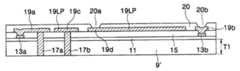
도 1은 본 발명의 일 실시예에 따른 멀티 칩 패키지를 도시한 단면도이고, 도 2는 도 1에 보여진 멀티 칩 패키지의 헬리클 안테나(helical antenna) 및 접지 쉴드(ground shield)를 도시한 사시도이다.1 is a cross-sectional view illustrating a multi-chip package according to an embodiment of the present invention, and FIG. 2 is a perspective view illustrating a helical antenna and a ground shield of the multi-chip package shown in FIG. 1. .
도 1 및 도 2를 참조하면, 패키지 보드(PB1) 상에 복수개의 반도체 칩들, 예 를 들면 제1 내지 제3 반도체 칩들(C1, C2, C3)이 차례로 적층된다. 상기 패키지 보드(PB1)는 앞면(fornt surface; 1FS) 및 뒷면(backside surface; 1BS)를 갖는 몸체(1)를 구비한다. 이에 더하여, 상기 패키지 보드(PB1)는 상기 앞면(1FS) 상에 배치된 제1 내지 제3 상부 보드 배선들(first to third upper board lines; 3a, 3b, 3c) 및 상기 뒷면(1BS) 상에 배치된 제1 내지 제3 하부 보드 배선들(5a, 5b, 5c)을 포함할 수 있다. 상기 제1 내지 제3 상부 보드 배선들(3a, 3b, 3c)은 각각 상기 몸체(1)를 관통하는 제1 내지 제3 보드 플러그들(도시하지 않음)을 통하여 상기 제1 내지 제3 하부 보드 배선들(5a, 5b, 5c)에 전기적으로 접속될 수 있다. 상기 제1 내지 제3 하부 보드 배선들(5a, 5b, 5c)은 각각 복수개의 볼들(53)과 접촉할 수 있다.1 and 2, a plurality of semiconductor chips, for example, first to third semiconductor chips C1, C2, and C3 are sequentially stacked on the package board PB1. The package board PB1 has a body 1 having a fornt surface 1FS and a backside surface 1BS. In addition, the package board PB1 is disposed on the first to third
상기 제1 내지 제3 반도체 칩들(C1, C2, C3)은 상기 패키지 보드(PB1)의 앞면(1FS) 상에 적층될 수 있다. 상기 제1 반도체 칩(C1)은 제1 반도체 기판(61), 상기 제1 반도체 기판(61) 상에 형성된 층간절연막(63), 및 상기 층간절연막(63) 상에 배치된 복수개의 하부 칩 패드들을 구비할 수 있다. 상기 하부 칩 패드들은 제1 및 제2 하부 칩 패드들(65a, 65b)을 포함할 수 있다. 이에 더하여, 상기 제1 반도체 칩(C1)은 상기 제1 및 제2 하부 칩 패드들(65a, 65b)을 덮도록 상기 층간절연막(63) 상에 제공된 하부 절연막(67), 상기 하부 절연막(67) 상에 배치된 복수개의 상부 칩 패드들, 및 상기 상부 칩 패드들을 덮도록 상기 하부 절연막(67) 상에 제공된 상부 절연막(71)을 구비할 수 있다. 상기 상부 칩 패드들은 제1 및 제2 상부 칩 패드들(69a, 69b)을 포함할 수 있다. 상기 제1 및 제2 상부 칩 패드들(69a, 69b)은 각각 상기 하부 절연막(67)을 관통하는 비아 홀들을 통하여 상기 제1 및 제2 하부 칩 패드들(65a, 65b)에 전기적으로 접속될 수 있다. 더 나아가서, 상기 제1 반도체 칩(C1)은 상기 상부 절연막(71) 상에 제공된 제1 열린 루프형 칩 배선(open loop-shaped chip line; 73LP)을 포함한다. 즉, 상기 제1 열린 루프형 칩 배선(73LP)은 제1 및 제2 단부들(73c, 73d)을 갖는다. 상기 제1 열린 루프형 칩 배선(73LP)은 재배치된 금속배선(redistributed metal line)일 수 있다.The first to third semiconductor chips C1, C2, and C3 may be stacked on the front surface 1FS of the package board PB1. The first semiconductor chip C1 may include a
상기 제1 하부 칩 패드(65a)가 송/수신 신호 패드(transceiving signal pad)인 경우에, 상기 제1 하부 칩 패드(65a)는 상기 제1 열린 루프형 칩 배선(73LP)의 상기 제1 단부(73c)에 전기적으로 접속된다. 상기 상부 절연막(71) 상에 본딩 패드(73b)가 추가로 배치될 수 있다. 상기 본딩 패드(73b)는 상기 상부 절연막(71)을 관통하는 비아 홀을 통하여 상기 제2 상부 칩 패드(69b)와 전기적으로 접속될 수 있다.When the first
상기 제1 반도체 칩(C1)이 와이어 본딩 칩인 경우에, 상기 본딩 패드(73b)는 제1 본딩 와이어(49a)를 통하여 상기 제1 상부 보드 배선(3a)에 전기적으로 접속될 수 있다. 상기 본딩 패드(73b)가 제공되지 않는 경우에, 상기 제1 본딩 와이어(49a)는 상기 제2 상부 칩 패드(69b)에 직접 연결될 수 있다. 상기 제1 반도체 칩(C1)은 제1 접착제(adhesive; 8)를 통하여 상기 패키지 보드(PB1)의 앞면(1FS)과 접촉할 수 있다.When the first semiconductor chip C1 is a wire bonding chip, the bonding pad 73b may be electrically connected to the first
상기 제2 반도체 칩(C2)은 제2 접착제(21)를 통하여 상기 제1 반도체 칩(C1)과 접촉할 수 있다. 상기 제2 반도체 칩(C2)은 제2 반도체 기판(23), 상기 제2 반 도체 기판(23) 상에 형성된 층간절연막(25), 및 상기 층간절연막(25) 상에 배치된 제1 및 제2 칩 패드들(27a, 27b)을 포함할 수 있다. 이에 더하여, 상기 제2 반도체 칩(C2)은 상기 칩 패드들(27a, 27b)을 덮도록 상기 층간절연막(25) 상에 형성된 절연막(29) 및 상기 절연막(29) 상에 배치된 제2 열린 루프형 칩 배선(33LP)를 포함할 수 있다. 상기 제2 열린 루프형 칩 배선(33LP)은 제1 및 제2 단부들(33c, 33d)을 갖는다. 상기 제2 열린 루프형 칩 배선(33LP) 역시 재배치된 금속배선일 수 있다. 더 나아가서, 상기 제2 반도체 칩(C2)은 상기 절연막(29) 상에 배치된 제1 및 제2 본딩 패드들(33a, 33b)을 포함할 수 있다. 상기 제1 및 제2 본딩 패드들(33a, 33b)은 각각 상기 절연막(29)을 관통하는 비아 홀들을 통하여 상기 제1 및 제2 칩 패드들(27a, 27b)에 전기적으로 접속될 수 있다.The second semiconductor chip C2 may contact the first semiconductor chip C1 through a
상기 제2 열린 루프형 칩 배선(33LP)의 상기 제1 단부(33c)는 제1 코넥터(31)를 통하여 상기 제1 열린 루프형 칩 배선(73LP)의 상기 제2 단부(73d)에 전기적으로 접속된다. 상기 제1 코넥터(31)는 도 1에 보여진 바와 같이 상기 제2 반도체 기판(23)을 관통하는 제1 금속 플러그일 수 있다.The
상기 제1 및 제2 본딩 패드들(33a, 33b)은 제2 본딩 와이어들(49b)을 통하여 상기 제2 상부 보드 배선들(3b)에 전기적으로 접속될 수 있다. 상기 제1 및 제2 본딩 패드들(33a, 33b)이 제공되지 않는 경우에, 상기 제2 본딩 와이어들(49b)은 상기 제1 및 제2 칩 패드들(27a, 27b)에 직접 접촉할 수 있다.The first and
상기 제3 반도체 칩(C3)은 제3 접착제(35)를 통하여 상기 제2 반도체 칩(C2)과 접촉할 수 있다. 상기 제3 반도체 칩(C3)은 상기 제2 반도체 칩(C2)과 동일한 구조를 가질 수 있다. 즉, 상기 제3 반도체 칩(C3)은 제3 반도체 기판(37), 상기 제3 반도체 기판(37) 상에 형성된 층간절연막(39), 및 상기 층간절연막(39) 상에 배치된 제1 및 제2 칩 패드들(41a, 41b)을 포함할 수 있다. 이에 더하여, 상기 제3 반도체 칩(C3)은 상기 칩 패드들(41a, 41b)을 덮도록 상기 층간절연막(39) 상에 형성된 절연막(43) 및 상기 절연막(43) 상에 배치된 제3 열린 루프형 칩 배선(47LP)를 포함할 수 있다. 상기 제3 열린 루프형 칩 배선(47LP)은 제1 및 제2 단부들(47c, 47d)을 갖는다. 상기 제3 열린 루프형 칩 배선(47LP) 역시 재배치된 금속배선일 수 있다. 더 나아가서, 상기 제3 반도체 칩(C3)은 상기 절연막(43) 상에 배치된 제1 및 제2 본딩 패드들(47a, 47b)을 포함할 수 있다. 상기 제1 및 제2 본딩 패드들(47a, 47b)은 각각 상기 절연막(43)을 관통하는 비아 홀들을 통하여 상기 제1 및 제2 칩 패드들(41a, 41b)에 전기적으로 접속될 수 있다.The third semiconductor chip C3 may be in contact with the second semiconductor chip C2 through a
상기 제3 열린 루프형 칩 배선(47LP)의 상기 제1 단부(47c)는 제2 코넥터(45)를 통하여 상기 제2 열린 루프형 칩 배선(33LP)의 상기 제2 단부(33d)에 전기적으로 접속된다. 상기 제2 코넥터(45)는 도 1에 보여진 바와 같이 상기 제3 반도체 기판(37)을 관통하는 제2 금속 플러그일 수 있다.The
상기 제1 및 제2 본딩 패드들(47a, 47b)은 제3 본딩 와이어들(49c)을 통하여 상기 제3 상부 보드 배선들(3c)에 전기적으로 접속될 수 있다. 상기 제1 및 제2 본딩 패드들(47a, 47b)이 제공되지 않는 경우에, 상기 제3 본딩 와이어들(49c)은 상기 제1 및 제2 칩 패드들(41a, 41b)에 직접 접촉할 수 있다. 상기 제1 내지 제3 반도체 칩들(C1, C2, C3) 및 상기 제1 내지 제3 본딩 와이어들(49a, 49b, 49c)은 도 1에 도시된 바와 같이 에폭시 성형 화합물(epoxy molding compound; 51)로 밀봉(encapsulate)될 수 있다.The first and
상술한 실시예에 따르면, 상기 제1 내지 제3 열린 루프형 칩 배선들(73LP, 33LP, 47LP), 상기 제1 코넥터(31) 및 상기 제2 코넥터(45)는 도 2에 도시된 바와 같이 상기 송/수신 신호 패드(65a)에 접속된 나선형의 안테나(spiral antenna), 즉 헬리클 안테나(helical antenna)를 구성할 수 있다.According to the above embodiment, the first to third open loop chip wires 73LP, 33LP, 47LP, the
상기 제1 반도체 칩(C1)은 상기 제1 반도체 기판(61) 내에 형성된 고주파 회로(monolithic microwave integrated circuit; MMIC)를 갖는 칩일 수 있다. 이 경우에, 상기 MMIC 칩이 동작하는 동안 상기 MMIC 칩으로부터 전자파 신호(electromagnetic wave signal)이 생성될 수 있고, 상기 전자파 신호는 상기 안테나의 송/수신 능력을 저하시킬 수 있다. 따라서, 상기 안테나의 성능이 상기 제1 반도체 칩(C1)으로부터의 전자파 신호에 기인하여 저하되는 것을 방지하기 위하여, 상기 제1 반도체 칩(C1)은 상기 제1 반도체 기판(61) 및 상기 제1 열린 루프형 칩 배선(73LP) 사이에 개재된 평판형 접지 쉴드(planar type ground shield; 69g)를 더 포함할 수 있다. 예를 들면, 상기 평판형 접지 쉴드(69g)는 상기 하부 절연막(67) 및 상기 상부 절연막(71) 사이에 배치될 수 있다. 상기 평판형 접지 쉴드(69g)는 도 1 및 도 2에 도시된 바와 같이 상기 제1 반도체 기판(61)과 중첩하도록 큰 면적을 갖는 접지 플레이트에 해당할 수 있다. 상기 접지 쉴드(69g)는 상기 층간절연막(65g) 상에 배치된 접지 칩 패드(65g)에 전기적으로 접속될 수 있다.The first semiconductor chip C1 may be a chip having a high frequency integrated circuit (MMIC) formed in the
도 3은 본 발명의 다른 실시예에 따른 멀티 칩 패키지를 도시한 단면도이고, 도 4는 도 3에 보여진 멀티 칩 패키지의 헬리클 안테나를 도시한 사시도이다.3 is a cross-sectional view illustrating a multi-chip package according to another embodiment of the present invention, and FIG. 4 is a perspective view illustrating a helical antenna of the multi-chip package shown in FIG. 3.
도 3 및 도 4를 참조하면, 패키지 보드(PB2) 상에 복수개의 반도체 칩들, 예를 들면 제1 내지 제3 반도체 칩들(C1', C2', C3')이 차례로 적층된다. 상기 제2 및 제3 반도체 칩들(C2', C3')은 각각 도 1에 보여진 상기 제2 및 제3 반도체 칩들(C2, C3)과 동일한 구조 및 동일한 구성요소들(components)을 가질 수 있다. 따라서, 본 실시예에서, 상기 제2 및 제3 반도체 칩들(C2', C3')에 대한 자세한 설명은 생략하기로 한다.3 and 4, a plurality of semiconductor chips, for example, first to third semiconductor chips C1 ′, C2 ′, and C3 ′, are sequentially stacked on the package board PB2. The second and third semiconductor chips C2 'and C3' may have the same structure and the same components as those of the second and third semiconductor chips C2 and C3 shown in FIG. 1, respectively. Therefore, in the present embodiment, detailed descriptions of the second and third semiconductor chips C2 'and C3' will be omitted.
상기 패키지 보드(PB2)는 도 1에 보여진 상기 패키지 보드(PB1)와 유사한 구조를 가질 수 있다. 예를 들면, 상기 패키지 보드(PB2)는 도 1에 보여진 상기 패키지 보드(PB1)의 몸체(1), 제1 내지 제3 상부 보드 배선들(3a, 3b, 3c), 제1 내지 제3 하부 보드 배선들(5a, 5b, 5c) 및 볼들(53)에 더하여 상기 앞면(1FS) 상에 배치된 제1 및 제2 보드 패드들(3d, 3e) 및 상기 몸체(1) 내에 배치된 열린 루프형 보드 배선(open loop-shaped board line; 7LP)를 더 포함할 수 있다. 상기 열린 루프형 보드 배선(7LP) 역시 제1 단부(7a) 및 제2 단부(7b)를 구비한다.The package board PB2 may have a structure similar to that of the package board PB1 shown in FIG. 1. For example, the package board PB2 may include a body 1 of the package board PB1, first to third
다른 실시예들에서, 상기 열린 루프형 보드 배선(7LP)은 상기 몸체(1)의 앞면(1FS) 또는 뒷면(1BS) 상에 배치될 수 있다. 상기 열린 루프형 보드 배선(7LP)이 상기 몸체(1)의 앞면(1FS) 상에 배치되는 경우에, 상기 열린 루프형 보드 배선(7LP)의 상기 제1 및 제2 단부들(7a, 7b)은 각각 상기 제1 및 제2 보드 패드들(3d, 3e)에 상응할 수 있다. 이와는 달리, 상기 열린 루프형 보드 배선(7LP)이 상기 몸체(1)의 벌크 영역 내에 또는 상기 몸체(1)의 뒷면(1BS) 상에 배치되는 경우에, 상 기 열린 루프형 보드 배선(7LP)의 상기 제1 및 제2 단부들(7a, 7b)은 각각 상기 제1 및 제2 보드 패드들(3d, 3e)에 전기적으로 접속될 수 있다.In other embodiments, the open loop board wiring 7LP may be disposed on the front surface 1FS or the rear surface 1BS of the body 1. When the open loop board wiring 7LP is disposed on the front surface 1FS of the body 1, the first and second ends 7a and 7b of the open loop board wiring 7LP. May correspond to the first and
상기 제1 반도체 칩(C1')은 상기 패키지 보드(PB2)의 앞면(1FS) 상에 적층될 수 있다. 상기 제1 반도체 칩(C1')은 제1 반도체 기판(9), 상기 제1 반도체 기판(9) 상에 형성된 층간절연막(11), 및 상기 층간절연막(11) 상에 배치된 복수개의 칩 패드들을 구비할 수 있다. 상기 칩 패드들은 제1 및 제2 칩 패드들(13a, 13b)을 포함할 수 있다. 이에 더하여, 상기 제1 반도체 칩(C1')은 상기 제1 및 제2 칩 패드들(13a, 13b)을 덮도록 상기 층간절연막(11) 상에 제공된 절연막(15), 상기 절연막(15) 상에 배치된 제1 열린 루프형 칩 배선(open loop-shaped chip line; 19LP)을 포함한다. 즉, 상기 제1 열린 루프형 칩 배선(19LP)은 제1 및 제2 단부들(19c, 19d)을 갖는다. 상기 제1 열린 루프형 칩 배선(19LP)은 재배치된 금속배선(redistributed metal line)일 수 있다. 더 나아가서, 상기 제1 반도체 칩(C1')은 상기 절연막(15) 상에 배치된 본딩 패드(19b)를 포함할 수 있다. 상기 본딩 패드(19b)는 상기 절연막(15)을 관통하는 비아 홀을 통하여 상기 제2 칩 패드(13b)에 전기적으로 접속될 수 있다.The first semiconductor chip C1 ′ may be stacked on the front surface 1FS of the package board PB2. The first semiconductor chip C1 ′ may include a
상기 제1 칩 패드(13a)가 송/수신 신호 패드(transceiving signal pad)인 경우에, 상기 제1 칩 패드(13a)는 국부배선(local line; 19a) 및 신호패드 코넥터(17a)를 통하여 상기 열린 루프형 보드 배선(7LP)의 상기 제1 단부(7a)에 전기적으로 접속될 수 있고, 상기 제1 열린 루프형 칩 배선(19LP)의 상기 제1 단부(19c)는 제1 코넥터(17b)를 통하여 상기 열린 루프형 보드 배선(7LP)의 상기 제2 단부(7b) 에 전기적으로 접속될 수 있다. 상기 국부배선(19a)은 도 3에 도시된 바와 같이 상기 절연막(15) 상에 배치된 금속배선일 수 있고, 상기 신호패드 코넥터(17a) 및 상기 제1 코넥터(17b)는 상기 제1 반도체 기판(9)을 관통하는 금속 플러그들일 수 있다.In the case where the
상기 제1 반도체 칩(C1')이 와이어 본딩 칩인 경우에, 상기 본딩 패드(19b)는 도 1에 보여진 실시예의 상기 제1 본딩 와이어(49a)를 통하여 상기 제1 상부 보드 배선(3a)에 전기적으로 접속될 수 있다. 상기 본딩 패드(19b)가 제공되지 않는 경우에, 상기 제1 본딩 와이어(49a)는 상기 제2 칩 패드(13b)에 직접 연결될 수 있다.When the first semiconductor chip C1 ′ is a wire bonding chip, the
상기 제2 반도체 칩(C2')은 상기 제1 반도체 칩(C1') 상에 적층된다. 상기 제2 반도체 칩(C2')은 상술한 바와 같이 도 1의 상기 제2 반도체 칩(C2)와 동일한 칩일 수 있다. 따라서, 상기 제2 열린 루프형 칩 배선(33LP)의 상기 제1 단부(33c)는 제2 코넥터(31')를 통하여 상기 제1 열린 루프형 칩 배선(19LP)의 상기 제2 단부(19d)에 전기적으로 접속될 수 있다. 상기 제2 코넥터(31')는 도 1에 보여진 실시예처럼 상기 제2 반도체 기판(23)을 관통하는 금속 플러그일 수 있다.The second semiconductor chip C2 'is stacked on the first semiconductor chip C1'. As described above, the second semiconductor chip C2 ′ may be the same chip as the second semiconductor chip C2 of FIG. 1. Accordingly, the
상기 제3 반도체 칩(C3')은 상기 제2 반도체 칩(C2') 상에 적층된다. 상기 제3 반도체 칩(C3')은 상술한 바와 같이 도 1의 상기 제3 반도체 칩(C3)과 동일한 구조를 가질 수 있다. 따라서, 상기 제3 열린 루프형 칩 배선(47LP)의 상기 제1 단부(47c)는 제3 코넥터(45')를 통하여 상기 제2 열린 루프형 칩 배선(33LP)의 상기 제2 단부(33d)에 전기적으로 접속될 수 있다. 상기 제3 코넥터(45')는 도 1에 보여 진 실시예처럼 상기 제3 반도체 기판(37)을 관통하는 금속 플러그일 수 있다.The third semiconductor chip C3 'is stacked on the second semiconductor chip C2'. As described above, the third semiconductor chip C3 ′ may have the same structure as the third semiconductor chip C3 of FIG. 1. Accordingly, the
결과적으로, 상기 열린 루프형 보드 배선(7LP), 상기 제1 내지 제3 열린 루프형 칩 배선들(19LP, 33LP, 47LP) 및 상기 코넥터들(17a, 17b, 31', 45')은 도 4에 도시된 바와 같이 상기 송/수신 신호 패드(13a)에 접속된 나선형의 안테나(spiral antenna), 즉 헬리클 안테나(helical antenna)를 구성할 수 있다.As a result, the open loop board wiring 7LP, the first to third open loop chip wirings 19LP, 33LP, 47LP, and the
본 실시예에 따르면, 상기 패키지 보드(PB2)의 내에 또는 상기 패키지 보드(PB2) 상에 상기 송/수신 신호 패드(13a)에 전기적으로 접속된 상기 열린 루프형 보드 배선이 제공된다. 그 결과, 본 실시예에 따른 멀티 칩 패키지의 안테나의 길이가 도 1 및 도 2에 보여진 실시예에 비하여 더욱 증가하므로 상기 안테나를 통하여 저주파 신호가 송/수신될 수 있다.According to the present embodiment, the open loop board wiring provided in the package board PB2 or on the package board PB2 is electrically connected to the transmit / receive
도 5는 본 발명의 또 다른 실시예에 따른 멀티 칩 패키지를 도시한 단면도이다.5 is a cross-sectional view illustrating a multi-chip package according to another embodiment of the present invention.
도 5를 참조하면, 패키지 보드(PB3) 상에 복수개의 상부 반도체 칩들, 예를 들면 제1 내지 제3 상부 반도체 칩들(FC1, C2", C3")이 차례로 적층된다. 상기 제2 및 제3 상부 반도체 칩들(C2", C3")은 각각 도 5에 도시된 바와 같이 도 1의 상기 제2 및 제3 반도체 칩들(C2, C3)과 동일한 구조 및 동일한 구성요소들을 가질 수 있다. 따라서, 본 실시예에서, 상기 제2 및 제3 상부 반도체 칩들(C2", C3")에 대한 자세한 설명은 생략하기로 한다.Referring to FIG. 5, a plurality of upper semiconductor chips, for example, first to third upper semiconductor chips FC1, C2 ″ and C3 ″ may be sequentially stacked on the package board PB3. The second and third upper semiconductor chips C2 "and C3" have the same structure and the same components as those of the second and third semiconductor chips C2 and C3 of FIG. 1, respectively, as shown in FIG. Can be. Therefore, in this embodiment, detailed description of the second and third upper semiconductor chips C2 "and C3" will be omitted.
상기 패키지 보드(PB3)는 앞면(fornt surface; 101FS) 및 뒷면(backside surface; 101BS)를 갖는 몸체(101)를 구비한다. 이에 더하여, 상기 패키지 보드 (PB3)는 상기 앞면(101FS) 상에 배치된 제1 내지 제3 상부 보드 배선들(first to third upper board lines; 103a, 103b, 103c) 및 상기 뒷면(101BS) 상에 배치된 제1 및 제2 하부 보드 배선들(105s, 105g)을 포함할 수 있다. 더 나아가서, 상기 패키지 보드(PB3)는 상기 앞면(101FS) 상에 배치된 상부 송/수신 보드 배선(103s)을 포함할 수 있다. 이 경우에, 상기 제1 하부 보드 배선(105s)은 상기 몸체(101)를 관통하는 보드 플러그(104s)를 통하여 상기 상부 송/수신 보드 배선(103s)에 전기적으로 접속될 수 있다. 즉, 상기 제1 하부 보드 배선(105s)은 하부 송/수신 보드 배선에 해당한다. 상기 제2 하부 보드 배선(105g)은 접지 보드 배선에 해당한다.The package board PB3 has a
본 실시예에서, 상기 패키지 보드(101)의 뒷면(101BS) 상에 하부 반도체 칩(FC2)이 제공될 수 있다. 상기 제1 상부 반도체 칩(FC1) 및 상기 하부 반도체 칩(FC2)은 각각 도 5에 도시된 바와 같이 제1 및 제2 플립 칩들일 수 있다. 그러나, 본 실시예는 플립 칩들을 갖는 멀티 칩 패키지에 한정되지 않는다. 다시 말해서, 상기 제1 상부 반도체 칩(FC1) 및 상기 하부 반도체 칩(FC2)중 적어도 어느 하나는 상기 제2 및 제3 상부 반도체 칩들(C2", C3")과 동일한 형태를 갖는 와이어 본딩 칩일 수 있다. 즉, 본 실시예는 본 발명이 적어도 하나의 플립 칩을 구비하는 멀티 칩 패키지에도 적용될 수 있음을 보여주기 위한 대표적인 예이다.In the present exemplary embodiment, the lower semiconductor chip FC2 may be provided on the rear surface 101BS of the
상기 제1 플립 칩(FC1)은 제1 반도체 기판(125), 상기 제1 반도체 기판(125)의 앞면 상에 형성된 층간절연막(127), 상기 층간절연막(127) 상에 배치된 칩 패드(129), 상기 칩 패드(129)를 덮도록 상기 층간절연막(127) 상에 형성된 하부 절연막(131) 및 상기 하부 절연막(131) 상에 제공된 제1 열린 루프형 칩 배선(135LP)을 포함할 수 있다. 또한, 상기 제1 플립 칩(FC1)은 상기 하부 절연막(131) 상에 배치된 본딩 패드(135a)를 더 포함할 수 있다. 상기 본딩 패드(135a)는 상기 하부 절연막(131)을 관통하는 비아 홀을 통하여 상기 칩 패드(129)에 전기적으로 접속될 수 있다. 이에 더하여, 상기 제1 플립 칩(FC1)은 상기 본딩 패드(135a) 및 상기 제1 열린 루프형 칩 배선(135LP)을 덮도록 상기 하부 절연막(131) 상에 형성된 상부 절연막(137)을 포함할 수 있다.The first flip chip FC1 may include a
더 나아가서, 상기 제1 플립 칩(FC1)은 상기 상부 절연막(137)을 관통하고 상기 상부 절연막(137)의 표면으로부터 돌출한 복수개의 금속 범프들(bumps)을 포함할 수 있다. 상기 범프들은 송/수신 신호 범프(139s) 및 복수개의 칩 범프들(139a)을 포함할 수 있다. 상기 송/수신 신호 범프(139s)는 상기 제1 열린 루프형 칩 배선(135LP)의 제1 단부(135b)에 전기적으로 접속될 수 있고, 상기 칩 범프들(139a)은 상기 제1 반도체 기판(125) 내에 형성된 내부 회로의 전원 패드들, 접지 패드들 및 신호 패드들에 각각 전기적으로 접속될 수 있다. 상기 송/수신 신호 범프(139s)는 상기 상부 송/수신 보드 배선(103s)에 접촉할 수 있고, 상기 복수개의 칩 범프들(139a)은 각각 그들에 대응하는 상기 제1 상부 보드 배선들(103a)에 접촉할 수 있다. 즉, 제1 플립 칩(FC1) 및 상기 패키지 보드(PB3) 사이에 제1 접착제(141)가 제공될 수 있다.In addition, the first flip chip FC1 may include a plurality of metal bumps penetrating the upper insulating
상기 제2 플립 칩(FC2)은 반도체 기판(109), 상기 반도체 기판(109)의 앞면 상에 형성된 층간절연막(111), 상기 층간절연막(111) 상에 배치된 칩 패드들을 포함할 수 있다. 상기 칩 패드들은 상기 반도체 기판(109) 내에 형성된 내부 회로의 송/수신 단자에 전기적으로 접속된 송/수신 신호 패드(113s)를 포함할 수 있다. 또한, 상기 칩 패드들은 제1 및 제2 접지 패드들(113g', 113g"), 전원 패드들(도시하지 않음) 및 신호 패드들(도시하지 않음)을 포함할 수 있다.The second flip chip FC2 may include a
이에 더하여, 상기 제2 플립 칩(FC2)은 상기 칩 패드들(113s, 113g', 113g")을 덮도록 상기 층간절연막(111) 상에 형성된 하부 절연막(115), 상기 하부 절연막(115) 상에 배치된 복수개의 본딩 패드들, 상기 본딩 패드들을 덮도록 상기 하부 절연막(115) 상에 형성된 상부 절연막(119) 및 상기 상부 절연막(119)을 관통하여 상기 본딩 패드들에 각각 접촉하는 복수개의 칩 범프들을 포함할 수 있다. 상기 본딩 패드들은 상기 송/수신 신호 패드(113s)에 전기적으로 접속된 송/수신 신호 본딩 패드(117s) 및 상기 제2 접지 패드(113g")에 전기적으로 접속된 접지 본딩 패드(117d)를 포함할 수 있고, 상기 칩 범프들은 상기 송/수신 신호 패드(113s) 및 상기 접지 본딩 패드(117d)에 각각 접촉하는 송/수신 신호 범프(121s) 및 상기 접지 범프(121g)를 포함할 수 있다.In addition, the second flip chip FC2 is formed on the lower insulating
상기 송/수신 신호 범프(121s)는 상기 하부 송/수신 보드 배선(105s)에 접촉할 수 있고, 상기 접지 범프(121g)는 상기 접지 보드 배선(105g)에 접촉할 수 있다. 결과적으로, 상기 제2 플립 칩(FC2)의 상기 송/수신 신호 패드(113s)는 상기 보드 플러그(104s)를 통하여 상기 제1 열린 루프형 칩 배선(135LP)의 제1 단부(135b)에 전기적으로 접속된다. 상기 제2 플립 칩(FC2) 및 상기 패키지 보드(PB3) 사이에 접착제(123)이 제공될 수 있다. 상기 제2 플립 칩(FC2)의 측벽들 및 상기 접착제(123)는 에폭시 수지(epoxy resin; 125)로 덮여질 수 있다. 이 경우에, 상기 제2 플립 칩(FC2)의 뒷면, 즉 상기 반도체 기판(109)의 뒷면은 노출된다.The transmit / receive
상기 제1 플립 칩(FC1)의 뒷면 상에 상기 제2 및 제3 상부 반도체 칩들(C2", C3")이 차례로 적층된다. 이 경우에, 상기 제2 열린 루프형 칩 배선(33LP)의 상기 제1 단부(33c)는 제1 및 제2 코넥터들(133, 31")을 통하여 상기 제1 열린 루프형 칩 배선(135LP)의 상기 제2 단부(135c)에 전기적으로 접속된다. 상기 제1 및 제2 코넥터들(133, 31")은 각각 도 5에 도시된 바와 같이 상기 제1 및 제2 반도체 기판들(125, 23)을 관통하는 제1 및 제2 금속 플러그들일 수 있다. 또한, 상기 제3 열린 루프형 칩 배선(47LP)의 상기 제1 단부(47c)는 제3 코넥터(45")를 통하여 상기 제2 열린 루프형 칩 배선(33LP)의 상기 제2 단부(33d)에 전기적으로 접속된다. 상기 제3 코넥터(45")는 상기 제3 반도체 기판(37)을 관통하는 제3 금속 플러그일 수 있다. 그 결과, 상기 제1 내지 제3 열린 루프형 칩 배선들(135LP, 33LP, 47LP), 상기 제1 내지 제3 코넥터들(133, 31", 45")은 상기 제2 플립 칩(FC2)의 상기 송/수신 신호 패드(113s)에 전기적으로 접속된 나선형의 안테나, 즉 헬리클 안테나를 구성한다.The second and third upper semiconductor chips C2 ″ and C3 ″ are sequentially stacked on the rear surface of the first flip chip FC1. In this case, the
상기 제2 플립 칩(FC2)이 상기 반도체 기판(109) 내에 형성된 고주파 회로(monolithic microwave integrated circuit; MMIC)를 갖는 반도체 칩인 경우에, 상기 MMIC 칩이 동작하는 동안 상기 MMIC 칩으로부터 전자파 신호(electromagnetic wave signal)이 생성될 수 있다. 따라서, 상기 안테나의 성능이 상기 제2 플립 칩(FC2)으로부터의 상기 전자파 신호에 기인하여 저하되는 것을 방지하기 위하여, 상기 제2 플립 칩(FC2)은 상기 반도체 기판(109) 상에 형성된 평판형 접지 쉴드 (117g)를 더 포함할 수 있다. 상기 평판형 접지 쉴드(117g)는 상기 하부 절연막(115) 및 상기 상부 절연막(119) 사이에 배치될 수 있다. 상기 평판형 접지 쉴드(117g)는 도 5에 도시된 바와 같이 상기 반도체 기판(109)과 중첩하도록 큰 면적을 갖는 접지 플레이트에 해당할 수 있다. 상기 접지 쉴드(117g)는 상기 제1 접지 패드(113g')에 전기적으로 접속될 수 있다.When the second flip chip FC2 is a semiconductor chip having a monolithic microwave integrated circuit (MMIC) formed in the
다른 실시예에서, 상기 제2 플립 칩(FC2)의 상기 접지 쉴드(117g) 대신에 상기 상기 패키지 보드(PB3)의 몸체(101) 내에 또는 상기 패키지 보드(PB3)의 표면 상에 배치된 평판형 접지 쉴드(107g)가 제공될 수 있다. 상기 접지 쉴드(107g)는 상기 제2 하부 보드 배선(105g)을 통하여 상기 제2 플립 칩(FC2)의 상기 제2 접지 패드(113g")에 전기적으로 접속될 수 있다.In another embodiment, a plate type disposed in the
도 6은 본 발명의 또 다른 실시예에 따른 멀티 적층 패키지(multi stack package)를 도시한 분해 사시도(exploded perspective view)이다.6 is an exploded perspective view showing a multi stack package according to another embodiment of the present invention.
도 6을 참조하면, 복수개의 패키지 보드들, 예를 들면 제1 내지 제3 패키지 보드들(PB11, PB22, PB33)이 차례로 적층된다. 상기 제1 패키지 보드(PB11)는 앞면 및 뒷면을 갖는 제1 몸체(151) 및 상기 제1 몸체(151)의 앞면 상에 배치된 제1 보드 배선(153a)을 구비할 수 있고, 상기 제2 패키지 보드(PB22)는 앞면 및 뒷면을 갖는 제2 몸체(161) 및 상기 제2 몸체(161)의 앞면 상에 배치된 제2 보드 배선들(163a, 163b)을 구비할 수 있다. 이와 마찬가지로, 상기 제3 패키지 보드(PB33)는 앞면 및 뒷면을 갖는 제3 몸체(171) 및 상기 제3 몸체(171)의 앞면 상에 배치된 제3 보드 배선(173a)을 구비할 수 있다.Referring to FIG. 6, a plurality of package boards, for example, first to third package boards PB11, PB22, and PB33 are sequentially stacked. The first package board PB11 may include a
상기 제1 패키지 보드(PB11)의 앞면 상에 제1 반도체 칩(C11)이 탑재되고, 상기 제2 패키지 보드(PB22)의 앞면 상에 제2 반도체 칩(C22)이 탑재된다. 이와 마찬가지로, 상기 제3 패키지 보드(PB33)의 앞면 상에 제3 반도체 칩(C33)이 탑재된다. 결과적으로, 상기 제1 반도체 칩(C11)은 상기 제1 및 제2 패키지 보드들(PB11, PB22) 사이에 제공되고, 상기 제2 반도체 칩(C22)은 상기 제2 및 제3 패키지 보드들(PB22, PB33) 사이에 제공된다.The first semiconductor chip C11 is mounted on the front surface of the first package board PB11, and the second semiconductor chip C22 is mounted on the front surface of the second package board PB22. Similarly, the third semiconductor chip C33 is mounted on the front surface of the third package board PB33. As a result, the first semiconductor chip C11 is provided between the first and second package boards PB11 and PB22, and the second semiconductor chip C22 is connected to the second and third package boards ( PB22, PB33).
상기 제1 반도체 칩(C11)은 제1 반도체 기판(155) 및 상기 제1 반도체 기판(155) 상에 제공된 제1 열린 루프형 칩 배선(157)을 포함하고, 상기 제2 반도체 칩(C22)은 제2 반도체 기판(165) 및 상기 제2 반도체 기판(165) 상에 제공된 제2 열린 루프형 칩 배선(167)을 포함한다. 이와 마찬가지로, 상기 제3 반도체 칩(C33)은 제3 반도체 기판(175) 및 상기 제3 반도체 기판(175) 상에 제공된 제3 열린 루프형 칩 배선(177)을 포함한다. 상기 제1 내지 제3 열린 루프형 칩 배선들(157, 167, 177)은 재배치된 금속 배선들일 수 있다.The first semiconductor chip C11 includes a
상기 제1 패키지 보드(PB11) 및 상기 제1 반도체 칩(C11)은 제1 반도체 패키지(PKG1)를 구성하고, 상기 제2 패키지 보드(PB22) 및 상기 제2 반도체 칩(C22)은 제2 반도체 패키지(PKG2)를 구성한다. 또한, 상기 제3 패키지 보드(PB33) 및 상기 제3 반도체 칩(C33)은 제3 반도체 패키지(PKG3)를 구성한다. 결과적으로, 본 실시예에 따른 반도체 패키지는 멀티 적층 패키지(multi stack package)에 해당한다.The first package board PB11 and the first semiconductor chip C11 constitute a first semiconductor package PKG1, and the second package board PB22 and the second semiconductor chip C22 are second semiconductors. Configure the package PKG2. In addition, the third package board PB33 and the third semiconductor chip C33 constitute a third semiconductor package PKG3. As a result, the semiconductor package according to the present embodiment corresponds to a multi stack package.
상기 제1 열린 루프형 칩 배선(157)의 제1 단부는 상기 제1 반도체 기판(155) 내에 형성된 내부회로의 송/수신 신호 패드(도시하지 않음)에 전기적으로 접 속될 수 있고, 상기 제1 열린 루프형 칩 배선(157)의 제2 단부는 제1 본딩 와이어(159)를 통하여 상기 제1 보드 배선(153a)에 전기적으로 접속될 수 있다. 상기 제2 열린 루프형 칩 배선(167)의 제1 단부는 제2 본딩 와이어(169a)를 통하여 상기 제2 보드 배선(163a)에 전기적으로 접속될 수 있고, 상기 제2 열린 루프형 칩 배선(167)의 제2 단부는 제2 본딩 와이어(169b)를 통하여 상기 제2 보드 배선(163b)에 전기적으로 접속될 수 있다. 또한, 상기 제3 열린 루프형 칩 배선(177)의 제1 단부는 제3 본딩 와이어(179)를 통하여 상기 제3 보드 배선(173a)에 전기적으로 접속될 수 있다.A first end of the first open
상기 제1 보드 배선(153a)은 상기 제2 패키지 보드(PB22)의 뒷면 상에 제공된 솔더 볼과 같은 제1 코넥터(160)를 통하여 상기 제2 보드 배선(163a)에 전기적으로 접속될 수 있고, 상기 제2 보드 배선(163b)은 상기 제3 패키지 보드(PB33)의 뒷면 상에 제공된 솔터 볼과 같은 제2 코넥터(170)를 통하여 상기 제3 보드 배선(173a)에 전기적으로 접속될 수 있다. 결과적으로, 상기 제1 내지 제3 열린 루프형 칩 배선들(157, 167, 177)은 상기 본딩 와이어들(159, 169a, 169b, 179), 상기 보드 배선들(153a, 163a, 163b, 163a) 및 상기 코넥터들(160, 170)과 함께 나선형의 안테나, 즉 헬리클 안테나를 구성한다.The
상기 제1 반도체 칩(C11)이 상기 제1 반도체 기판(155) 내에 형성된 고주파 회로(monolithic microwave integrated circuit; MMIC)를 갖는 반도체 칩인 경우에, 상기 MMIC 칩이 동작하는 동안 상기 MMIC 칩으로부터 전자파 신호(electromagnetic wave signal)이 생성될 수 있다. 따라서, 상기 안테나의 성능이 상기 제1 반도체 칩(C11)으로부터의 상기 전자파 신호에 기인하여 저하되는 것을 방지하기 위하여, 상기 제1 반도체 칩(C11)은 상기 제1 반도체 기판(155) 상에 형성된 평판형 접지 쉴드(도시하지 않음)를 더 포함할 수 있다. 상기 평판형 접지 쉴드는 상기 제1 열린 루프형 칩 배선(157) 및 상기 제1 반도체 기판(155) 사이에 배치될 수 있다. 상기 접지 쉴드는 도 1, 도 2 및 도 5를 참조하여 설명된 바와 같이 상기 제1 반도체 기판(155)과 중첩하도록 큰 면적을 갖는 접지 플레이트에 해당할 수 있다.When the first semiconductor chip C11 is a semiconductor chip having a monolithic microwave integrated circuit (MMIC) formed in the
도 7은 본 발명의 또 다른 실시예에 따른 멀티 칩 패키지를 도시한 단면도이다. 본 실시예는 변압기의 유도 코일을 갖는 멀티 칩 패키지를 설명하기 위한 대표적인 예(exemplary embodiment)이다.7 is a cross-sectional view illustrating a multi-chip package according to another embodiment of the present invention. This embodiment is an exemplary embodiment for describing a multi-chip package having an induction coil of a transformer.
도 7을 참조하면, 본 실시예에 따른 멀티 칩 패키지는 도 3에 보여진 실시예에 따른 멀티 칩 패키지의 구성요소들에 더하여 상기 제2 및 제3 반도체 기판들(23, 37)을 각각 관통하는 코넥터들(31p, 45p) 및 상기 제1 반도체 기판(9) 상에 배치된 제3 칩 패드(13c)를 포함한다. 상기 제3 칩 패드(13c)는 상기 코넥터들(31p, 45p)을 통하여 상기 제3 열린 루프형 칩 배선(47LP)의 상기 제2 단부(47d)에 전기적으로 접속될 수 있다. 그 결과, 상기 제1 내지 제3 열린 루프형 칩 배선들(19LP, 33LP, 47LP), 상기 열린 루프형 보드 배선(7LP), 상기 코넥터들(17a, 17b, 31', 45', 31p, 45p)은 상기 제1 칩 패드(13a) 및 상기 제3 칩 패드(13c)에 접속된 변압기의 유도 코일(induction coil)을 구성한다. 본 실시예에 따르면, 상기 유도 코일은 솔레노이드 코일(solenoid coil)에 해당할 수 있다.Referring to FIG. 7, the multi-chip package according to the present embodiment penetrates through the second and
상기 열린 루프형 보드 배선(7LP)이 제공되지 않으면, 상기 제1 열린 루프형 칩 배선(19LP)의 상기 제1 단부(19c)는 상기 제1 칩 패드(13a)에 전기적으로 접속될 수 있다. 이 경우에, 상기 유도 코일은 상기 제1 내지 제3 열린 루프형 칩 배선들(19LP, 33LP, 47LP) 및 상기 코넥터들(31', 45', 31p, 45p)만으로 구성될 수 있다.If the open loop board wiring 7LP is not provided, the
상술한 실시예에 따른 멀티 칩 패키지는 집적회로 카드(IC card) 등에 채택될 수 있다. 이 경우에, 상기 집적회로 카드가 외부 자계(MF)를 제공하는 시스템 단말기에 접촉되면, 상기 유도 코일은 상기 집적회로 카드 내의 내부회로를 구동시키는 전원 전압을 생성시킬 수 있다. 이에 따라, 상기 단말기에 접속된 메인 시스템 및 상기 카드 사이에 원하는 통신이 실행될 수 있다.The multi-chip package according to the above-described embodiment may be adopted as an integrated circuit card (IC card). In this case, when the integrated circuit card is in contact with a system terminal providing an external magnetic field (MF), the induction coil may generate a power supply voltage for driving the internal circuit in the integrated circuit card. Accordingly, desired communication can be executed between the main system and the card connected to the terminal.
도 8 내지 도 12는 도 3에 보여진 상기 제1 반도체 칩(C1')의 제조방법을 설명하기 위한 단면도들이다. 비록 본 실시예에 따른 방법이 도 3의 상기 제1 반도체 칩(C1')을 제조하는 방법을 예로 하여 설명될지라도, 본 발명이 본 발명의 사상 및 범위 내에서 상기 제1 반도체 칩(C1') 이외의 다른 반도체 칩들(예를 들면, 도 3의 제2 및 제3 반도체 칩들(C2', C3'))을 제조하는 방법들에 적용될 수 있음은 명백하다.8 to 12 are cross-sectional views illustrating a method of manufacturing the first semiconductor chip C1 ′ shown in FIG. 3. Although the method according to the present embodiment is described by taking the method of manufacturing the first semiconductor chip C1 'of FIG. 3 as an example, the present invention is within the spirit and scope of the present invention. It is apparent that the present invention can be applied to methods for manufacturing other semiconductor chips (eg, the second and third semiconductor chips C2 'and C3' of FIG. 3).
도 8 및 도 9를 참조하면, 제1 두께(T1)를 갖는 초기 반도체 기판(9') 상에 층간절연막(11)을 형성한다. 상기 층간절연막(11) 상에 복수개의 칩 패드들, 예를 들면 제1 및 제2 칩 패드들(13a, 13b)을 형성한다. 이어서, 상기 칩 패드들(13a, 13b)을 갖는 기판 상에 하부 절연막(15)을 형성한다. 상기 하부 절연막(15), 상기 층간절연막(11) 및 상기 초기 반도체 기판(9')을 식각 공정을 사용하여 패터닝하여 상기 하부 절연막(15), 상기 층간절연막(11) 및 상기 초기 반도체 기판(9')을 관통하는 제1 및 제2 홀들(17a, 17b)을 형성한다. 상기 식각 공정은 건식 식각 공정일 수 있다. 상기 제1 및 제2 홀들(17a, 17b) 내에 각각 제1 코넥터(17a) 및 제2 코넥터(17b)를 선택적으로 형성한다. 상기 코넥터들(17a, 17b)은 전기 도금법(electroplating technique)을 사용하여 형성할 수 있다. 이 경우에, 상기 코넥터들(17a, 17b)은 금속 플러그들일 수 있다.8 and 9, an
도 10 및 도 11을 참조하면, 상기 하부 절연막(15)을 패터닝하여 상기 제1 및 제2 칩 패드들(13a, 13b)을 각각 노출시키는 제1 및 제2 비아 홀들(15a, 15b)을 형성한다. 상기 제1 및 제2 비아 홀들(15a, 15b)을 갖는 기판 상에 재배치된 금속막을 형성한다. 상기 재배치된 금속막을 패터닝하여 열린 루프형 칩 배선(19LP), 국부배선(19a) 및 본딩 패드(19b)를 형성한다. 상기 열린 루프형 칩 배선(19LP)은 제1 및 제2 단부들(19c, 19d)을 갖도록 형성된다.10 and 11, the lower insulating
상기 열린 루프형 칩 배선(19LP)은 상기 제1 단부(19c)가 상기 제1 코넥터(17b)를 덮도록 형성될 수 있다. 상기 본딩 패드(19b)는 상기 제2 칩 패드(13b)를 노출시키는 상기 제2 비아 홀(도 10의 15b)을 덮도록 형성된다. 또한, 상기 제1 칩 패드(13a)가 송/수신 신호 패드(13a)일 때, 상기 국부 배선(19a)은 상기 송/수신 신호 패드(13a)를 노출시키는 상기 제1 비아 홀(도 10의 15a) 및 상기 제1 코넥터(17a)의 상부면을 덮도록 형성될 수 있다. 이 경우에, 상기 제1 코넥터(17a)는 신호패드 코넥터에 해당할 수 있다. 결과적으로, 상기 제1 칩 패드(13a)는 상기 국부 배선(19a)을 통하여 상기 제1 코넥터(17a)에 전기적으로 접속된다.The open loop chip wiring 19LP may be formed such that the
상기 열린 루프형 칩 배선(19LP)을 갖는 기판 상에 상부 절연막(20)을 추가로 형성할 수 있다. 상기 상부 절연막(20)을 패터닝하여 상기 열린 루프형 칩 배선(19LP)의 상기 제2 단부(19d)를 노출시키는 제1 개구부(first opening; 20a) 및 상기 본딩 패드(19b)를 노출시키는 제2 개구부(20b)를 형성할 수 있다.An upper insulating
도 12를 참조하면, 상기 초기 반도체 기판(9')의 뒷면을 선택적으로 폴리슁하여 상기 제1 두께(T1)보다 작은 제2 두께(T2)를 갖는 반도체 기판(9)을 형성한다. 그 결과, 상기 제1 및 제2 코넥터들(17a, 17b)은 상기 반도체 기판(9)의 뒷면으로부터 상대적으로 돌출할 수 있다. 즉, 상기 제1 및 제2 코넥터들(17a, 17b)은 돌출부들(P)을 가질 수 있다.Referring to FIG. 12, the back surface of the
상술한 실시예들에 따르면, 반도체 패키지 내의 반도체 칩들 상에 열린 루프형 칩 배선들이 제공되고, 이들 열린 루프형 칩 배선들의 단부들을 서로 접속시키는 코넥터들이 제공된다. 이에 따라, 상기 열린 루프형 칩 배선들 및 상기 코넥터들을 사용하여 상기 반도체 칩들중 어느 하나의 송/수신 신호 패드에 접속된 나선형 안테나를 구현할 수 있다. 또한, 상기 나선형 안테나의 일 단에 전기적으로 접속된 추가 코넥터들이 제공될 수 있고, 상기 추가 코넥터들은 상기 반도체 칩들중 어느 하나의 칩 패드에 전기적으로 접속될 수 있다. 이 경우에, 상기 나선형 안테나 및 상기 추가 코넥터들을 사용하여 변압기의 유도 코일을 구현할 수 있다. 결과적으로, 본 발명에 따르면, 반도체 패키지 크기의 증가 없이 고성능 안테나 및/또 는 고성능 변압기를 제공할 수 있다.According to the above-described embodiments, open loop chip wirings are provided on semiconductor chips in a semiconductor package, and connectors are provided for connecting ends of these open loop chip wirings to each other. Accordingly, the spiral antenna connected to the transmit / receive signal pad of any one of the semiconductor chips may be implemented using the open loop chip wires and the connectors. Further, additional connectors may be provided that are electrically connected to one end of the spiral antenna, and the additional connectors may be electrically connected to a chip pad of any one of the semiconductor chips. In this case, the spiral antenna and the additional connectors can be used to implement the induction coil of the transformer. As a result, according to the present invention, it is possible to provide a high performance antenna and / or a high performance transformer without increasing the semiconductor package size.
Claims (31)
Translated fromKoreanPriority Applications (4)
| Application Number | Priority Date | Filing Date | Title |
|---|---|---|---|
| KR20060017903AKR100714310B1 (en) | 2006-02-23 | 2006-02-23 | Semiconductor Packages with Transformer or Antenna |
| US11/541,779US7868462B2 (en) | 2006-02-23 | 2006-10-03 | Semiconductor package including transformer or antenna |
| CNB2006101494998ACN100487892C (en) | 2006-02-23 | 2006-11-21 | Semiconductor packages including transformer or antenna |
| JP2007002293AJP2007227897A (en) | 2006-02-23 | 2007-01-10 | Semiconductor package with transformer or antenna |
Applications Claiming Priority (1)
| Application Number | Priority Date | Filing Date | Title |
|---|---|---|---|
| KR20060017903AKR100714310B1 (en) | 2006-02-23 | 2006-02-23 | Semiconductor Packages with Transformer or Antenna |
Publications (1)
| Publication Number | Publication Date |
|---|---|
| KR100714310B1true KR100714310B1 (en) | 2007-05-02 |
Family
ID=38269642
Family Applications (1)
| Application Number | Title | Priority Date | Filing Date |
|---|---|---|---|
| KR20060017903AActiveKR100714310B1 (en) | 2006-02-23 | 2006-02-23 | Semiconductor Packages with Transformer or Antenna |
Country Status (4)
| Country | Link |
|---|---|
| US (1) | US7868462B2 (en) |
| JP (1) | JP2007227897A (en) |
| KR (1) | KR100714310B1 (en) |
| CN (1) | CN100487892C (en) |
Cited By (5)
| Publication number | Priority date | Publication date | Assignee | Title |
|---|---|---|---|---|
| KR100836536B1 (en) | 2006-12-21 | 2008-06-10 | 한국과학기술원 | SIP with reduced effect on conductor antenna and its design method |
| KR101099587B1 (en) | 2011-04-20 | 2011-12-28 | 앰코 테크놀로지 코리아 주식회사 | Stacked chip semiconductor package using TS |
| US8445996B2 (en) | 2007-10-11 | 2013-05-21 | Samsung Electronics Co., Ltd. | Semiconductor package |
| KR101481576B1 (en)* | 2008-10-06 | 2015-01-14 | 삼성전자주식회사 | Semiconductor package |
| JP2018157150A (en)* | 2017-03-21 | 2018-10-04 | 東芝メモリ株式会社 | Semiconductor device |
Families Citing this family (65)
| Publication number | Priority date | Publication date | Assignee | Title |
|---|---|---|---|---|
| JP5076909B2 (en)* | 2006-01-24 | 2012-11-21 | 日本電気株式会社 | Integrated circuit device |
| US7791199B2 (en) | 2006-11-22 | 2010-09-07 | Tessera, Inc. | Packaged semiconductor chips |
| US8569876B2 (en)* | 2006-11-22 | 2013-10-29 | Tessera, Inc. | Packaged semiconductor chips with array |
| US8405196B2 (en) | 2007-03-05 | 2013-03-26 | DigitalOptics Corporation Europe Limited | Chips having rear contacts connected by through vias to front contacts |
| SG148901A1 (en) | 2007-07-09 | 2009-01-29 | Micron Technology Inc | Packaged semiconductor assemblies and methods for manufacturing such assemblies |
| KR100906065B1 (en)* | 2007-07-12 | 2009-07-03 | 주식회사 동부하이텍 | Semiconductor chip, manufacturing method thereof and laminated package having same |
| JP2009021499A (en)* | 2007-07-13 | 2009-01-29 | Toshiba Corp | Multilayer semiconductor device |
| WO2009017835A2 (en) | 2007-07-31 | 2009-02-05 | Tessera, Inc. | Semiconductor packaging process using through silicon vias |
| JP4833192B2 (en)* | 2007-12-27 | 2011-12-07 | 新光電気工業株式会社 | Electronic equipment |
| US8253241B2 (en)* | 2008-05-20 | 2012-08-28 | Infineon Technologies Ag | Electronic module |
| US8129266B2 (en)* | 2008-07-09 | 2012-03-06 | Semiconductor Componenets Industries, LLC | Method of forming a shielded semiconductor device and structure therefor |
| US8183673B2 (en)* | 2008-10-21 | 2012-05-22 | Samsung Electronics Co., Ltd. | Through-silicon via structures providing reduced solder spreading and methods of fabricating the same |
| US8049319B2 (en)* | 2008-10-24 | 2011-11-01 | Electronics And Telecommunications Research Institute | Ultra wideband system-on-package |
| KR20100048610A (en) | 2008-10-31 | 2010-05-11 | 삼성전자주식회사 | Semiconductor fackage and forming method of the same |
| US20100127937A1 (en)* | 2008-11-25 | 2010-05-27 | Qualcomm Incorporated | Antenna Integrated in a Semiconductor Chip |
| US8278749B2 (en) | 2009-01-30 | 2012-10-02 | Infineon Technologies Ag | Integrated antennas in wafer level package |
| JP2011082450A (en) | 2009-10-09 | 2011-04-21 | Elpida Memory Inc | Semiconductor device, and information processing system with the same |
| US8035218B2 (en)* | 2009-11-03 | 2011-10-11 | Intel Corporation | Microelectronic package and method of manufacturing same |
| KR20110050964A (en)* | 2009-11-09 | 2011-05-17 | 주식회사 하이닉스반도체 | Semiconductor package and manufacturing method thereof |
| US9999129B2 (en)* | 2009-11-12 | 2018-06-12 | Intel Corporation | Microelectronic device and method of manufacturing same |
| US8304917B2 (en)* | 2009-12-03 | 2012-11-06 | Powertech Technology Inc. | Multi-chip stacked package and its mother chip to save interposer |
| KR20110078189A (en)* | 2009-12-30 | 2011-07-07 | 삼성전자주식회사 | Memory card and memory system having semiconductor chips of stacked structure |
| US8970000B2 (en)* | 2010-01-18 | 2015-03-03 | Infineon Technologies Austria Ag | Signal transmission arrangement |
| US8199518B1 (en) | 2010-02-18 | 2012-06-12 | Amkor Technology, Inc. | Top feature package and method |
| US8946886B1 (en) | 2010-05-13 | 2015-02-03 | Amkor Technology, Inc. | Shielded electronic component package and method |
| KR20110133945A (en)* | 2010-06-08 | 2011-12-14 | 삼성전자주식회사 | Stacked package and its manufacturing method |
| US8791575B2 (en) | 2010-07-23 | 2014-07-29 | Tessera, Inc. | Microelectronic elements having metallic pads overlying vias |
| US8796135B2 (en) | 2010-07-23 | 2014-08-05 | Tessera, Inc. | Microelectronic elements with rear contacts connected with via first or via middle structures |
| US9640437B2 (en) | 2010-07-23 | 2017-05-02 | Tessera, Inc. | Methods of forming semiconductor elements using micro-abrasive particle stream |
| US9007273B2 (en) | 2010-09-09 | 2015-04-14 | Advances Semiconductor Engineering, Inc. | Semiconductor package integrated with conformal shield and antenna |
| US8847380B2 (en) | 2010-09-17 | 2014-09-30 | Tessera, Inc. | Staged via formation from both sides of chip |
| US8610259B2 (en) | 2010-09-17 | 2013-12-17 | Tessera, Inc. | Multi-function and shielded 3D interconnects |
| JP5172925B2 (en)* | 2010-09-24 | 2013-03-27 | 株式会社東芝 | Wireless device |
| US8451618B2 (en) | 2010-10-28 | 2013-05-28 | Infineon Technologies Ag | Integrated antennas in wafer level package |
| US8736066B2 (en) | 2010-12-02 | 2014-05-27 | Tessera, Inc. | Stacked microelectronic assemby with TSVS formed in stages and carrier above chip |
| US8587126B2 (en) | 2010-12-02 | 2013-11-19 | Tessera, Inc. | Stacked microelectronic assembly with TSVs formed in stages with plural active chips |
| KR101711045B1 (en)* | 2010-12-02 | 2017-03-02 | 삼성전자 주식회사 | Stacked Package Structure |
| US8637968B2 (en) | 2010-12-02 | 2014-01-28 | Tessera, Inc. | Stacked microelectronic assembly having interposer connecting active chips |
| US8610264B2 (en) | 2010-12-08 | 2013-12-17 | Tessera, Inc. | Compliant interconnects in wafers |
| JP5414749B2 (en) | 2011-07-13 | 2014-02-12 | 株式会社東芝 | Wireless device |
| JP5417389B2 (en) | 2011-07-13 | 2014-02-12 | 株式会社東芝 | Wireless device |
| US8659126B2 (en)* | 2011-12-07 | 2014-02-25 | Taiwan Semiconductor Manufacturing Company, Ltd. | Integrated circuit ground shielding structure |
| US8610247B2 (en) | 2011-12-30 | 2013-12-17 | Taiwan Semiconductor Manufacturing Company, Ltd. | Structure and method for a transformer with magnetic features |
| US20130113089A1 (en)* | 2011-11-09 | 2013-05-09 | Azurewave Technologies, Inc. | Module ic package structure having a metal shielding function for preventing electrical malfunction induced by short-circuit |
| US8786060B2 (en)* | 2012-05-04 | 2014-07-22 | Advanced Semiconductor Engineering, Inc. | Semiconductor package integrated with conformal shield and antenna |
| US9136213B2 (en) | 2012-08-02 | 2015-09-15 | Infineon Technologies Ag | Integrated system and method of making the integrated system |
| CN103811444B (en)* | 2012-11-07 | 2016-11-23 | 环旭电子股份有限公司 | The manufacture method of electronic installation, system-in-package module and system-in-package module |
| JP6121705B2 (en) | 2012-12-12 | 2017-04-26 | 株式会社東芝 | Wireless device |
| JP6027905B2 (en)* | 2013-01-31 | 2016-11-16 | 新光電気工業株式会社 | Semiconductor device |
| US9978688B2 (en) | 2013-02-28 | 2018-05-22 | Advanced Semiconductor Engineering, Inc. | Semiconductor package having a waveguide antenna and manufacturing method thereof |
| CN103227170A (en)* | 2013-03-29 | 2013-07-31 | 日月光半导体制造股份有限公司 | Stacked semiconductor structure and manufacturing method thereof |
| KR102053349B1 (en)* | 2013-05-16 | 2019-12-06 | 삼성전자주식회사 | Semiconductor package |
| US20150179555A1 (en)* | 2013-12-20 | 2015-06-25 | Sung Soo Kim | Integrated circuit packaging system with vialess substrate and method of manufacture thereof |
| KR20150088453A (en)* | 2014-01-24 | 2015-08-03 | 한국전자통신연구원 | Multiband plasma loop antenna |
| US9190345B1 (en)* | 2014-03-28 | 2015-11-17 | Taiwan Semiconductor Manufacturing Company, Ltd. | Semiconductor devices and methods of manufacture thereof |
| KR101729378B1 (en)* | 2014-05-30 | 2017-04-21 | 타이완 세미콘덕터 매뉴팩쳐링 컴퍼니 리미티드 | Semiconductor devices and methods of manufacture thereof |
| US10236115B2 (en)* | 2014-06-16 | 2019-03-19 | Stmicroelectronics S.R.L. | Integrated transformer |
| US11717178B2 (en)* | 2016-01-25 | 2023-08-08 | Kyocera Corporation | Measurement sensor package and measurement sensor |
| US10243272B2 (en)* | 2016-04-27 | 2019-03-26 | Getac Technology Corporation | Antenna device and antenna module having the antenna device |
| US10079222B2 (en)* | 2016-11-16 | 2018-09-18 | Powertech Technology Inc. | Package-on-package structure and manufacturing method thereof |
| US10177095B2 (en) | 2017-03-24 | 2019-01-08 | Amkor Technology, Inc. | Semiconductor device and method of manufacturing thereof |
| DE102019110570B4 (en)* | 2019-04-24 | 2023-05-25 | Infineon Technologies Ag | MAGNETIC FIELD SENSOR PACKAGE WITH INTEGRATED PASSIVE COMPONENT |
| US11164826B2 (en) | 2019-08-30 | 2021-11-02 | Nxp Usa, Inc. | Packaged integrated circuit having stacked die and method for making |
| SE2030349A1 (en)* | 2020-11-30 | 2021-12-21 | Gapwaves Ab | Improved ultra-wideband circular-polarized radiation element with integrated feeding |
| EP4420165A4 (en)* | 2021-10-19 | 2025-08-13 | Adeia Semiconductor Bonding Technologies Inc | Stacked inductors in multi-chip stacking |
Citations (4)
| Publication number | Priority date | Publication date | Assignee | Title |
|---|---|---|---|---|
| KR20010056582A (en)* | 1999-12-16 | 2001-07-04 | 김덕중 | Method for macturing ltcc with the antener |
| KR20010082044A (en)* | 2000-02-18 | 2001-08-29 | 크리스티안 그레그와르 | Packaged integrated circuit |
| KR20020081089A (en)* | 2001-04-17 | 2002-10-26 | 가시오게산키 가부시키가이샤 | Semiconductor Device |
| JP2004342948A (en) | 2003-05-19 | 2004-12-02 | Tdk Corp | Electronic component module |
Family Cites Families (16)
| Publication number | Priority date | Publication date | Assignee | Title |
|---|---|---|---|---|
| US5023624A (en)* | 1988-10-26 | 1991-06-11 | Harris Corporation | Microwave chip carrier package having cover-mounted antenna element |
| US6440773B1 (en)* | 1997-12-22 | 2002-08-27 | Hitachi, Ltd. | Semiconductor device |
| CN1243294A (en) | 1998-07-28 | 2000-02-02 | 东芝株式会社 | Integrated circuit card, data read-write device and radio mark and mfg. method therefor |
| US6351033B1 (en)* | 1999-10-06 | 2002-02-26 | Agere Systems Guardian Corp. | Multifunction lead frame and integrated circuit package incorporating the same |
| US6304232B1 (en)* | 2000-02-24 | 2001-10-16 | The Goodyear Tire & Rubber Company | Circuit module |
| US6686649B1 (en)* | 2001-05-14 | 2004-02-03 | Amkor Technology, Inc. | Multi-chip semiconductor package with integral shield and antenna |
| US6897830B2 (en) | 2002-07-04 | 2005-05-24 | Antenna Tech, Inc. | Multi-band helical antenna |
| US6933603B2 (en)* | 2002-07-11 | 2005-08-23 | Teledyne Technologies Incorporated | Multi-substrate layer semiconductor packages and method for making same |
| US20040061213A1 (en)* | 2002-09-17 | 2004-04-01 | Chippac, Inc. | Semiconductor multi-package module having package stacked over die-up flip chip ball grid array package and having wire bond interconnect between stacked packages |
| AU2003298595A1 (en)* | 2002-10-08 | 2004-05-04 | Chippac, Inc. | Semiconductor stacked multi-package module having inverted second package |
| JP4381113B2 (en) | 2003-11-27 | 2009-12-09 | 三洋電機株式会社 | Antenna duplexer |
| CN2676405Y (en) | 2003-12-10 | 2005-02-02 | 立卫科技股份有限公司 | Die Attach Adhesive |
| KR100585226B1 (en) | 2004-03-10 | 2006-06-01 | 삼성전자주식회사 | Semiconductor package having heat sink and laminated package using same |
| US20060214271A1 (en)* | 2005-03-23 | 2006-09-28 | Jeremy Loraine | Device and applications for passive RF components in leadframes |
| US7763963B2 (en)* | 2005-05-04 | 2010-07-27 | Stats Chippac Ltd. | Stacked package semiconductor module having packages stacked in a cavity in the module substrate |
| US7312519B2 (en)* | 2006-01-12 | 2007-12-25 | Stats Chippac Ltd. | Stacked integrated circuit package-in-package system |
- 2006
- 2006-02-23KRKR20060017903Apatent/KR100714310B1/enactiveActive
- 2006-10-03USUS11/541,779patent/US7868462B2/enactiveActive
- 2006-11-21CNCNB2006101494998Apatent/CN100487892C/enactiveActive
- 2007
- 2007-01-10JPJP2007002293Apatent/JP2007227897A/enactivePending
Patent Citations (4)
| Publication number | Priority date | Publication date | Assignee | Title |
|---|---|---|---|---|
| KR20010056582A (en)* | 1999-12-16 | 2001-07-04 | 김덕중 | Method for macturing ltcc with the antener |
| KR20010082044A (en)* | 2000-02-18 | 2001-08-29 | 크리스티안 그레그와르 | Packaged integrated circuit |
| KR20020081089A (en)* | 2001-04-17 | 2002-10-26 | 가시오게산키 가부시키가이샤 | Semiconductor Device |
| JP2004342948A (en) | 2003-05-19 | 2004-12-02 | Tdk Corp | Electronic component module |
Cited By (5)
| Publication number | Priority date | Publication date | Assignee | Title |
|---|---|---|---|---|
| KR100836536B1 (en) | 2006-12-21 | 2008-06-10 | 한국과학기술원 | SIP with reduced effect on conductor antenna and its design method |
| US8445996B2 (en) | 2007-10-11 | 2013-05-21 | Samsung Electronics Co., Ltd. | Semiconductor package |
| KR101481576B1 (en)* | 2008-10-06 | 2015-01-14 | 삼성전자주식회사 | Semiconductor package |
| KR101099587B1 (en) | 2011-04-20 | 2011-12-28 | 앰코 테크놀로지 코리아 주식회사 | Stacked chip semiconductor package using TS |
| JP2018157150A (en)* | 2017-03-21 | 2018-10-04 | 東芝メモリ株式会社 | Semiconductor device |
Also Published As
| Publication number | Publication date |
|---|---|
| JP2007227897A (en) | 2007-09-06 |
| US20070194427A1 (en) | 2007-08-23 |
| CN100487892C (en) | 2009-05-13 |
| CN101026145A (en) | 2007-08-29 |
| US7868462B2 (en) | 2011-01-11 |
Similar Documents
| Publication | Publication Date | Title |
|---|---|---|
| KR100714310B1 (en) | Semiconductor Packages with Transformer or Antenna | |
| US12095142B2 (en) | Semiconductor package having discrete antenna device | |
| US9076789B2 (en) | Semiconductor device having a high frequency external connection electrode positioned within a via hole | |
| KR101719630B1 (en) | Semiconductor package and package on package comprising them | |
| US8587096B2 (en) | Semiconductor device including shielding layer and fabrication method thereof | |
| US7696629B2 (en) | Chip-stacked package structure | |
| US9030021B2 (en) | Printed circuit board having hexagonally aligned bump pads for substrate of semiconductor package, and semiconductor package including the same | |
| US20020036338A1 (en) | Stacked type semiconductor device | |
| KR20050047748A (en) | Semiconductor chip package having decoupling capacitor and manufacturing method thereof | |
| US7772694B2 (en) | Integrated circuit module and method of packaging same | |
| CN103187396A (en) | Semiconductor package with ultra-thin interposer without through-semiconductor vias | |
| JP2002510148A (en) | Semiconductor component having a plurality of substrate layers and at least one semiconductor chip and a method for manufacturing the semiconductor component | |
| US8692386B2 (en) | Semiconductor device, method of manufacturing semiconductor device, and electronic device | |
| US7626265B2 (en) | Semiconductor package having flexible lead connection plate for electrically connecting base and chip | |
| US20080078571A1 (en) | Device mounting board and semiconductor module | |
| KR20090131255A (en) | Circuit device and method of manufacturing the circuit device | |
| US20090283894A1 (en) | Semiconductor chip package and printed circuit board having through interconnections | |
| TWI887641B (en) | Antenna package | |
| US7884465B2 (en) | Semiconductor package with passive elements embedded within a semiconductor chip | |
| JP2004022667A (en) | Semiconductor module structure | |
| CN111863756B (en) | Packaging structure and semiconductor device with same | |
| US20250079319A1 (en) | Semiconductor package and method of fabricating the same | |
| US20250006703A1 (en) | Semiconductor package | |
| US20250105097A1 (en) | Semiconductor package including a dummy chip and method of manufacturing the same | |
| KR101811738B1 (en) | Enhanced stacked microelectric assemblies with central contacts |
Legal Events
| Date | Code | Title | Description |
|---|---|---|---|
| A201 | Request for examination | ||
| PA0109 | Patent application | Patent event code:PA01091R01D Comment text:Patent Application Patent event date:20060223 | |
| PA0201 | Request for examination | ||
| E701 | Decision to grant or registration of patent right | ||
| PE0701 | Decision of registration | Patent event code:PE07011S01D Comment text:Decision to Grant Registration Patent event date:20070317 | |
| GRNT | Written decision to grant | ||
| PR0701 | Registration of establishment | Comment text:Registration of Establishment Patent event date:20070426 Patent event code:PR07011E01D | |
| PR1002 | Payment of registration fee | Payment date:20070427 End annual number:3 Start annual number:1 | |
| PG1601 | Publication of registration | ||
| PR1001 | Payment of annual fee | Payment date:20100413 Start annual number:4 End annual number:4 | |
| PR1001 | Payment of annual fee | Payment date:20110405 Start annual number:5 End annual number:5 | |
| FPAY | Annual fee payment | ||
| PR1001 | Payment of annual fee | Payment date:20120402 Start annual number:6 End annual number:6 | |
| FPAY | Annual fee payment | ||
| PR1001 | Payment of annual fee | Payment date:20130329 Start annual number:7 End annual number:7 | |
| PR1001 | Payment of annual fee | Payment date:20140331 Start annual number:8 End annual number:8 | |
| PR1001 | Payment of annual fee | Payment date:20150331 Start annual number:9 End annual number:9 | |
| PR1001 | Payment of annual fee | Payment date:20160331 Start annual number:10 End annual number:10 | |
| PR1001 | Payment of annual fee | Payment date:20170331 Start annual number:11 End annual number:11 | |
| PR1001 | Payment of annual fee | Payment date:20180330 Start annual number:12 End annual number:12 | |
| FPAY | Annual fee payment | Payment date:20190329 Year of fee payment:13 | |
| PR1001 | Payment of annual fee | Payment date:20190329 Start annual number:13 End annual number:13 | |
| PR1001 | Payment of annual fee | Payment date:20200330 Start annual number:14 End annual number:14 | |
| PR1001 | Payment of annual fee | Payment date:20210329 Start annual number:15 End annual number:15 | |
| PR1001 | Payment of annual fee | Payment date:20220323 Start annual number:16 End annual number:16 | |
| PR1001 | Payment of annual fee | Payment date:20230327 Start annual number:17 End annual number:17 | |
| PR1001 | Payment of annual fee | Payment date:20240325 Start annual number:18 End annual number:18 |