KR100714305B1 - Formation method of self-aligned double pattern - Google Patents
Formation method of self-aligned double patternDownload PDFInfo
- Publication number
- KR100714305B1 KR100714305B1KR1020050129928AKR20050129928AKR100714305B1KR 100714305 B1KR100714305 B1KR 100714305B1KR 1020050129928 AKR1020050129928 AKR 1020050129928AKR 20050129928 AKR20050129928 AKR 20050129928AKR 100714305 B1KR100714305 B1KR 100714305B1
- Authority
- KR
- South Korea
- Prior art keywords
- mask pattern
- layer
- mask
- pattern
- forming
- Prior art date
- Legal status (The legal status is an assumption and is not a legal conclusion. Google has not performed a legal analysis and makes no representation as to the accuracy of the status listed.)
- Active
Links
Images


Classifications
- H—ELECTRICITY
- H01—ELECTRIC ELEMENTS
- H01L—SEMICONDUCTOR DEVICES NOT COVERED BY CLASS H10
- H01L21/00—Processes or apparatus adapted for the manufacture or treatment of semiconductor or solid state devices or of parts thereof
- H01L21/02—Manufacture or treatment of semiconductor devices or of parts thereof
- H01L21/027—Making masks on semiconductor bodies for further photolithographic processing not provided for in group H01L21/18 or H01L21/34
- H01L21/0271—Making masks on semiconductor bodies for further photolithographic processing not provided for in group H01L21/18 or H01L21/34 comprising organic layers
- H01L21/0273—Making masks on semiconductor bodies for further photolithographic processing not provided for in group H01L21/18 or H01L21/34 comprising organic layers characterised by the treatment of photoresist layers
- H—ELECTRICITY
- H01—ELECTRIC ELEMENTS
- H01L—SEMICONDUCTOR DEVICES NOT COVERED BY CLASS H10
- H01L21/00—Processes or apparatus adapted for the manufacture or treatment of semiconductor or solid state devices or of parts thereof
- H01L21/02—Manufacture or treatment of semiconductor devices or of parts thereof
- H01L21/04—Manufacture or treatment of semiconductor devices or of parts thereof the devices having potential barriers, e.g. a PN junction, depletion layer or carrier concentration layer
- H01L21/18—Manufacture or treatment of semiconductor devices or of parts thereof the devices having potential barriers, e.g. a PN junction, depletion layer or carrier concentration layer the devices having semiconductor bodies comprising elements of Group IV of the Periodic Table or AIIIBV compounds with or without impurities, e.g. doping materials
- H01L21/30—Treatment of semiconductor bodies using processes or apparatus not provided for in groups H01L21/20 - H01L21/26
- H01L21/302—Treatment of semiconductor bodies using processes or apparatus not provided for in groups H01L21/20 - H01L21/26 to change their surface-physical characteristics or shape, e.g. etching, polishing, cutting
- H01L21/306—Chemical or electrical treatment, e.g. electrolytic etching
- H01L21/308—Chemical or electrical treatment, e.g. electrolytic etching using masks
- H01L21/3083—Chemical or electrical treatment, e.g. electrolytic etching using masks characterised by their size, orientation, disposition, behaviour, shape, in horizontal or vertical plane
- H01L21/3086—Chemical or electrical treatment, e.g. electrolytic etching using masks characterised by their size, orientation, disposition, behaviour, shape, in horizontal or vertical plane characterised by the process involved to create the mask, e.g. lift-off masks, sidewalls, or to modify the mask, e.g. pre-treatment, post-treatment
- H—ELECTRICITY
- H01—ELECTRIC ELEMENTS
- H01L—SEMICONDUCTOR DEVICES NOT COVERED BY CLASS H10
- H01L21/00—Processes or apparatus adapted for the manufacture or treatment of semiconductor or solid state devices or of parts thereof
- H01L21/02—Manufacture or treatment of semiconductor devices or of parts thereof
- H01L21/027—Making masks on semiconductor bodies for further photolithographic processing not provided for in group H01L21/18 or H01L21/34
- H01L21/033—Making masks on semiconductor bodies for further photolithographic processing not provided for in group H01L21/18 or H01L21/34 comprising inorganic layers
- H01L21/0334—Making masks on semiconductor bodies for further photolithographic processing not provided for in group H01L21/18 or H01L21/34 comprising inorganic layers characterised by their size, orientation, disposition, behaviour, shape, in horizontal or vertical plane
- H01L21/0337—Making masks on semiconductor bodies for further photolithographic processing not provided for in group H01L21/18 or H01L21/34 comprising inorganic layers characterised by their size, orientation, disposition, behaviour, shape, in horizontal or vertical plane characterised by the process involved to create the mask, e.g. lift-off masks, sidewalls, or to modify the mask, e.g. pre-treatment, post-treatment
- H—ELECTRICITY
- H01—ELECTRIC ELEMENTS
- H01L—SEMICONDUCTOR DEVICES NOT COVERED BY CLASS H10
- H01L21/00—Processes or apparatus adapted for the manufacture or treatment of semiconductor or solid state devices or of parts thereof
- H01L21/02—Manufacture or treatment of semiconductor devices or of parts thereof
- H01L21/027—Making masks on semiconductor bodies for further photolithographic processing not provided for in group H01L21/18 or H01L21/34
- H01L21/033—Making masks on semiconductor bodies for further photolithographic processing not provided for in group H01L21/18 or H01L21/34 comprising inorganic layers
- H01L21/0334—Making masks on semiconductor bodies for further photolithographic processing not provided for in group H01L21/18 or H01L21/34 comprising inorganic layers characterised by their size, orientation, disposition, behaviour, shape, in horizontal or vertical plane
- H01L21/0338—Process specially adapted to improve the resolution of the mask
- H—ELECTRICITY
- H01—ELECTRIC ELEMENTS
- H01L—SEMICONDUCTOR DEVICES NOT COVERED BY CLASS H10
- H01L21/00—Processes or apparatus adapted for the manufacture or treatment of semiconductor or solid state devices or of parts thereof
- H01L21/02—Manufacture or treatment of semiconductor devices or of parts thereof
- H01L21/04—Manufacture or treatment of semiconductor devices or of parts thereof the devices having potential barriers, e.g. a PN junction, depletion layer or carrier concentration layer
- H01L21/18—Manufacture or treatment of semiconductor devices or of parts thereof the devices having potential barriers, e.g. a PN junction, depletion layer or carrier concentration layer the devices having semiconductor bodies comprising elements of Group IV of the Periodic Table or AIIIBV compounds with or without impurities, e.g. doping materials
- H01L21/30—Treatment of semiconductor bodies using processes or apparatus not provided for in groups H01L21/20 - H01L21/26
- H01L21/302—Treatment of semiconductor bodies using processes or apparatus not provided for in groups H01L21/20 - H01L21/26 to change their surface-physical characteristics or shape, e.g. etching, polishing, cutting
- H01L21/306—Chemical or electrical treatment, e.g. electrolytic etching
- H01L21/308—Chemical or electrical treatment, e.g. electrolytic etching using masks
- H01L21/3083—Chemical or electrical treatment, e.g. electrolytic etching using masks characterised by their size, orientation, disposition, behaviour, shape, in horizontal or vertical plane
- H01L21/3088—Process specially adapted to improve the resolution of the mask
- Y—GENERAL TAGGING OF NEW TECHNOLOGICAL DEVELOPMENTS; GENERAL TAGGING OF CROSS-SECTIONAL TECHNOLOGIES SPANNING OVER SEVERAL SECTIONS OF THE IPC; TECHNICAL SUBJECTS COVERED BY FORMER USPC CROSS-REFERENCE ART COLLECTIONS [XRACs] AND DIGESTS
- Y10—TECHNICAL SUBJECTS COVERED BY FORMER USPC
- Y10S—TECHNICAL SUBJECTS COVERED BY FORMER USPC CROSS-REFERENCE ART COLLECTIONS [XRACs] AND DIGESTS
- Y10S438/00—Semiconductor device manufacturing: process
- Y10S438/914—Doping
- Y10S438/925—Fluid growth doping control, e.g. delta doping
Landscapes
- Engineering & Computer Science (AREA)
- Physics & Mathematics (AREA)
- Condensed Matter Physics & Semiconductors (AREA)
- General Physics & Mathematics (AREA)
- Manufacturing & Machinery (AREA)
- Computer Hardware Design (AREA)
- Microelectronics & Electronic Packaging (AREA)
- Power Engineering (AREA)
- Chemical & Material Sciences (AREA)
- Inorganic Chemistry (AREA)
- Internal Circuitry In Semiconductor Integrated Circuit Devices (AREA)
- Drying Of Semiconductors (AREA)
Abstract
Translated fromKoreanDescription
Translated fromKorean도 1a 내지 도 1h는 본 발명의 제1 실시예에 따라 자기정렬 이중패터닝 방법을 도시한 단면도들이다.1A to 1H are cross-sectional views illustrating a self-aligned double patterning method according to a first embodiment of the present invention.
도 2a 내지 도 2h는 본 발명의 제2 실시예에 따라 소자 분리 트렌치를 형성하는 방법을 도시한 단면도들이다.2A-2H are cross-sectional views illustrating a method of forming an isolation trench in accordance with a second embodiment of the present invention.
* 도면의 주요부분에 대한 부호의 설명 *Explanation of symbols on the main parts of the drawings
100, 200 : 반도체 기판110 : 하지막100, 200: semiconductor substrate 110: base film
120, 210 : 실리콘 질화막135, 225 : 제1 마스크 패턴120 and 210:
155, 245 : 제2 마스크 패턴150 : 하지막 패턴155 and 245
260 : 트렌치260 trench
본 발명은 패턴의 형성 방법에 관한 것으로, 더욱 상세하게는 자기정렬 이중패터닝(Self Align Double Patterning) 방법에 관한 것이다.The present invention relates to a method of forming a pattern, and more particularly, to a method of Self Align Double Patterning.
최근 반도체 소자의 집적도가 향상됨에 따라 좁은 면적에 많은 소자를 집적 시키기 위한 기술이 요구되고 있다. 좁은 면적에 많은 소자들을 집적시키기 위해서는 반도체 기판 상에 형성되는 소자의 크기를 축소하여야 한다. 그러나 소자의 크기를 축소하는 것은 일정한 한계를 가지고 있다.Recently, as the degree of integration of semiconductor devices is improved, a technology for integrating many devices in a small area is required. In order to integrate many devices in a small area, the size of devices formed on a semiconductor substrate must be reduced. However, reducing the size of the device has certain limitations.
즉, 소자의 크기를 결정하는 포토리소그래피 공정에서 광원이 가지는 파장의 한계에 의해 소자의 크기를 축소하는 것은 일정한 한계가 있다. 상기 포토리소그래피 공정에서 광원으로 사용되는 엑시머 레이저(Excimer laser)는 KrF 엑시머 레이저 및 ArF 엑시머 레이저 등이 사용된다. ArF 엑시머 레이저는 193nm의 파장을 가지며 0.07um 내지 0.15um의 피쳐 사이즈(Feature size)를 가진다. 또한, KrF 엑시머 레이저는 248nm의 파장을 가지며 0.13um 내지 0.25um의 피쳐 사이즈(Feature size)를 가진다. 이외에도 I-line 또는 G-line 등의 수은 램프가 광원으로 사용되기도 한다.That is, in the photolithography process for determining the size of the device, the size of the device is reduced due to the limitation of the wavelength of the light source. As the excimer laser used as the light source in the photolithography process, an KrF excimer laser, an ArF excimer laser, or the like is used. The ArF excimer laser has a wavelength of 193 nm and a feature size of 0.07 um to 0.15 um. In addition, the KrF excimer laser has a wavelength of 248 nm and a feature size of 0.13 um to 0.25 um. In addition, mercury lamps such as I-line or G-line may be used as light sources.
파장이 짧은 광원을 사용하는 경우, 높은 해상도(resolution)로 인해 더욱 미세한 패턴을 형성할 수 있다. 그러나, 파장이 짧은 광원을 이용하는 경우, 상기 광원을 흡수하여 화학 증폭(Chemical Amplification)을 수행할 수 있는 포토레지스트가 구비되지 않는 경우가 대부분이다. 즉, 파장이 짧은 광원을 사용한다하더라도, 이에 대한 감광성(photo-sensitivity)을 가진 포토레지스트가 개발되어야 한다.When using a light source with a short wavelength, a higher resolution may form a finer pattern. However, when a light source having a short wavelength is used, a photoresist capable of absorbing the light source and performing chemical amplification is mostly not provided. That is, even if a light source having a short wavelength is used, a photoresist having photo-sensitivity to it should be developed.
상술한 문제점을 개선하기 위해 최근에 개발되고 있는 미세 패턴 형성 방법이 자기정렬 이중패터닝이다. 상기 자기정렬 이중패터닝은 포토리소그래피 장비가 가지는 해상도를 이용하고, 상기 해상도에 의해 형성되는 패턴에 비해 2배의 집적 도를 가진 패턴을 형성하는 방법이다.In order to improve the above-mentioned problem, a method of forming a fine pattern recently developed is self-aligned double patterning. The self-aligned double patterning is a method of forming a pattern having a density twice as large as a pattern formed by the resolution using photolithography equipment.
자기정렬 이중패터닝에 대해서는 대한민국 등록특허 제165399호, 대한민국 등록특허 제281891호 및 미국 등록특허 제6638441호에 개시된다.Self-aligned double patterning is disclosed in Korean Patent No. 165399, Korean Patent No. 281891 and US Patent No. 6638441.
대한민국 등록특허 제165399호는 금속 패턴의 형성 방법을 개시한다. 먼저, 기판 상에 제1 도전층 패턴, 제1 절연층 패턴, 제2 도전층 패턴 및 제2 절연층 패턴이 순차적으로 형성되고, 제2 절연층 패턴을 식각 마스크로 하여 식각이 수행된다. 식각에 의해 형성된 제2 절연층 패턴 사이의 공간에는 제3 절연층 패턴이 매립된다. 상술한 과정을 통해 해상도의 한계와 동일한 간격을 가지는 제1 도전층 패턴 사이에는 제2 도전성 패턴이 형성되는 자기정렬 이중패터닝이 수행된다.Republic of Korea Patent No. 165399 discloses a method of forming a metal pattern. First, a first conductive layer pattern, a first insulating layer pattern, a second conductive layer pattern, and a second insulating layer pattern are sequentially formed on a substrate, and etching is performed using the second insulating layer pattern as an etching mask. The third insulating layer pattern is buried in the space between the second insulating layer patterns formed by etching. Through the above-described process, self-aligned double patterning in which a second conductive pattern is formed between the first conductive layer patterns having the same interval as the resolution limit is performed.
대한민국 등록특허 제281891호에는 반도체장치의 배선패턴 형성 방법이 개시된다. 먼저, 제1 배선 패턴을 형성하고, 제1 배선 패턴 상부 및 패턴들 사이에는 절연막이 도포된다. 상기 절연막은 제1 배선 패턴 하부의 과식각 깊이와 동일한 두께를 가지고 형성된다. 또한, 절연막 상부에는 배선 물질층이 형성된다. 상기 배선 물질층에 대해 평탄화 공정을 수행하면, 제1 배선 패턴들 사이에 형성된 제2 배선 패턴을 얻을 수 있다.Korean Patent No. 281891 discloses a method of forming a wiring pattern of a semiconductor device. First, a first wiring pattern is formed, and an insulating film is coated over the first wiring pattern and the patterns. The insulating layer is formed to have the same thickness as the over-etching depth under the first wiring pattern. In addition, a wiring material layer is formed on the insulating film. When the planarization process is performed on the wiring material layer, a second wiring pattern formed between the first wiring patterns may be obtained.
또한, 미국 등록특허 제6638441호는 배선 사이의 간격을 감소시키는 방법이 개시된다. 먼저, 포토레지스트 패턴을 형성하고, 상기 포토레지스트 패턴 상에 유전층을 형성한다. 상기 유전층에 대해 에치백 공정을 수행하여 유전층 하부의 기판을 노출시킨다. 또한, 유전층 사이에 반사 방지막(Bottom Anti-reflection coating)을 매립한 후, 포토레지스트 패턴을 제거한다. 제거된 공간에는 다른 반사 방지막 및 유전층을 매립하고, 표면에 대한 평탄화 공정을 수행한다. 상술한 과정을 통해 기판 상에 포토레지스트 패턴보다 2배로 밀집된 밀도를 가진 유전층 패턴들을 얻을 수 있다.In addition, U.S. Patent No. 6,638,441 discloses a method for reducing the spacing between wirings. First, a photoresist pattern is formed, and a dielectric layer is formed on the photoresist pattern. An etch back process is performed on the dielectric layer to expose the substrate under the dielectric layer. Further, after embedding a bottom anti-reflection coating between the dielectric layers, the photoresist pattern is removed. Another anti-reflection film and dielectric layer are embedded in the removed space, and the surface planarization process is performed. Through the above-described process, dielectric layer patterns having a density twice as large as that of the photoresist pattern may be obtained on the substrate.
상술한 특허들은 다수의 문제점들을 가진다. 즉, 대한민국 등록특허 제165399호는 금속 패턴들의 높이가 일치하지 않으며, 대한민국 등록특허 제281891호는 제2 배선 패턴이 기판과의 전기적 연결을 달성할 수 없는 문제를 가진다. 또한, 미국 등록특허 제6638441호는 유전막 패턴의 형성 방법만을 개시할 뿐이며, 다수의 증착 공정을 이용하여 패턴의 형성 방법이 복잡하고, 제조 공정상 패턴의 형성이 곤란해진다는 문제가 있다.The aforementioned patents have a number of problems. That is, the Republic of Korea Patent No. 165399 does not match the height of the metal patterns, the Republic of Korea Patent No. 281891 has a problem that the second wiring pattern can not achieve an electrical connection with the substrate. In addition, US Patent No. 6664441 discloses only a method of forming a dielectric film pattern, there is a problem that a method of forming a pattern using a plurality of deposition processes is complicated, and it is difficult to form a pattern in a manufacturing process.
상기와 같은 문제점을 해결하기 위한 본 발명의 목적은, 유기 희생막을 사용하여 자기정렬 이중 패터닝을 구현하는 방법을 제공하는데 있다.An object of the present invention for solving the above problems is to provide a method for implementing self-aligned double patterning using an organic sacrificial film.
상기 목적을 달성하기 위한 본 발명은, 하지막 상부에 제1 마스크 패턴을 형성하는 단계; 상기 제1 마스크 패턴 및 상기 하지막 상에 희생층을 콘포말하게 형성하는 단계; 상기 희생층의 측벽들 사이에 매립된 제2 마스크 패턴을 형성하는 단계; 상기 희생층을 식각하여 상기 제2 마스크 패턴 하부에 잔류하는 희생 패턴을 형성하는 단계; 상기 제1 마스크 패턴 및 상기 제2 마스크 패턴 사이의 이격 공간을 매립하는 유기 희생막을 형성하는 단계; 상기 제1 마스크 패턴 및 상기 제2 마스크 패턴의 상부면이 동일 레벨을 가지도록 상기 유기 희생막에 대해 평탄화 공정 을 수행하는 단계; 및 상기 제1 마스크 패턴 및 상기 제2 마스크 패턴을 식각 마스크로 상기 하지막을 식각하여 하지막 패턴을 형성하는 단계를 포함하는 자기정렬 이중패턴의 형성방법을 제공한다.The present invention for achieving the above object, forming a first mask pattern on the base film; Conformally forming a sacrificial layer on the first mask pattern and the underlayer; Forming a second mask pattern buried between sidewalls of the sacrificial layer; Etching the sacrificial layer to form a sacrificial pattern remaining under the second mask pattern; Forming an organic sacrificial layer filling a space between the first mask pattern and the second mask pattern; Performing a planarization process on the organic sacrificial layer such that upper surfaces of the first mask pattern and the second mask pattern have the same level; And etching the base layer using the first mask pattern and the second mask pattern as an etch mask to form an underlayer pattern.
또한, 본 발명의 상기 목적은, 반도체 기판 상에 제1 마스크 패턴을 형성하는 단계; 상기 제1 마스크 패턴 및 상기 반도체 기판 상에 증착층을 형성하는 단계; 상기 증착층의 측벽들 사이에 매립된 제2 마스크 패턴을 형성하는 단계; 상기 증착층을 식각하여 상기 제2 마스크 패턴 하부에 잔류하는 증착층 패턴을 형성하는 단계; 상기 제1 마스크 패턴 및 상기 제2 마스크 패턴 사이의 이격 공간을 매립하는 유기 희생막을 형성하는 단계; 상기 제1 마스크 패턴 및 상기 제2 마스크 패턴의 상부면이 동일 레벨을 가지도록 상기 유기 희생막에 대한 평탄화 공정을 수행하는 단계; 및 상기 제1 마스크 패턴 및 상기 제2 마스크 패턴을 식각 마스크로 하여 상기 반도체 기판을 식각하여, 트렌치를 형성하는 단계를 포함하는 자기정렬 이중패턴의 형성방법을 제공한다.In addition, the object of the present invention, forming a first mask pattern on a semiconductor substrate; Forming a deposition layer on the first mask pattern and the semiconductor substrate; Forming a second mask pattern buried between sidewalls of the deposition layer; Etching the deposition layer to form a deposition layer pattern remaining under the second mask pattern; Forming an organic sacrificial layer filling a space between the first mask pattern and the second mask pattern; Performing a planarization process on the organic sacrificial layer such that upper surfaces of the first mask pattern and the second mask pattern have the same level; And etching the semiconductor substrate using the first mask pattern and the second mask pattern as an etching mask to form a trench.
이하, 본 발명에 따른 바람직한 실시예를 첨부된 도면을 참조하여 상세하게 설명한다.Hereinafter, exemplary embodiments of the present invention will be described in detail with reference to the accompanying drawings.
제1 실시예First embodiment
도 1a 내지 도 1h는 본 발명의 제1 실시예에 따라 자기정렬 이중패터닝 방법을 도시한 단면도들이다.1A to 1H are cross-sectional views illustrating a self-aligned double patterning method according to a first embodiment of the present invention.
도 1a를 참조하면, 반도체 기판(100) 상에 하지막(110)이 형성되고, 하지막 (110) 상부에 제1 마스크층(130)이 형성된다. 바람직하게는 상기 하지막(110)과 제1 마스크층(130) 사이에는 실리콘 질화막(SiN)(120)이 개재된다. 상기 하지막(110)은 이후의 공정에서 패터닝되며, 제1 마스크층(130)은 상기 하지막(110)의 패터닝시 식각 마스크로 사용된다.Referring to FIG. 1A, a
도 1b를 참조하면, 제1 마스크 패턴(135)이 형성되고, 노출된 실리콘 질화막(120) 상부 및 상기 제1 마스크 패턴(135) 상에 희생층(140)이 형성된다.Referring to FIG. 1B, a
상기 제1 마스크 패턴(135)의 폭 W1은 상기 제1 마스크 패턴(135)의 피치(pitch) P1의 1/4임이 바람직하다. 또한, 희생층(140)의 측벽들 사이의 거리 W2는 제1 마스크 패턴(135)의 피치(pitch) P1의 1/4임이 바람직하다.The width W1 of the
상기 도 1a에서, 제1 마스크층(130) 상에 포토레지스트를 도포하고, 통상적인 포토리소그래피 공정에 의해 포토레지스트 패턴을 형성한다. 형성된 포토레지스트 패턴을 식각 마스크로 하여 제1 마스크층(130)에 대해 식각을 수행하면, 제1 마스크 패턴(135)이 형성된다. 상기 제1 마스크 패턴(135)의 형성을 위한 식각 공정시 상기 실리콘 질화막(120)은 식각 저지막으로 작용함이 바람직하다.In FIG. 1A, a photoresist is applied on the
이어서, 노출된 실리콘 질화막(120) 및 제1 마스크 패턴(135) 상에 희생층(140)을 형성한다. 상기 희생층(140)은 실리콘 질화막(120) 및 제1 마스크 패턴(135) 상에 콘포말하게 형성됨이 바람직하다. 만일, 상기 질리콘 질화막(120)이 개재되지 않는 경우, 상기 희생층(140)은 노출된 하지막(110) 및 제1 마스크 패턴(135) 상에 형성된다.Subsequently, a
도 1c를 참조하면, 하지막(110) 상부에 형성된 제1 마스크 패턴(135), 희생 층(140) 및 희생층(140) 상부에 형성된 제2 마스크층(150)이 도시된다.Referring to FIG. 1C, the
먼저, 도 1b에서 희생층(140) 상부를 제2 마스크층(150)으로 도포한다. 또한, 상기 희생층(140)은 제1 마스크 패턴(135) 및 제2 마스크층(150)에 대해 식각 선택비를 가지는 물질로 형성됨이 바람직하다. 또한, 상기 제2 마스크층(150)은 상기 제1 마스크 패턴(135)과 동일한 식각 선택비를 가진 물질로 구성된다. 바람직하게는 상기 제2 마스크층(150)은 상기 제1 마스크 패턴(135)과 동일한 물질로 구성된다.First, in FIG. 1B, an upper portion of the
도 1d를 참조하면, 실리콘 질화막(120) 상부에 제1 마스크 패턴(135)이 형성되고, 제1 마스크 패턴들(135) 사이에는 제2 마스크 패턴(155)이 형성되며, 제1 마스크 패턴(135) 및 제2 마스크 패턴(155) 사이에는 희생층(140)이 구비된다.Referring to FIG. 1D, a
상기 도 1c에 도시된 제2 마스크층(150)에 대해 평탄화 공정을 수행하여 희생층(140) 상부의 제2 마스크층(150)을 제거하고, 희생층(140) 표면의 일부를 노출시킨다. 또한, 상기 희생층(140) 측벽들 사이에 개재된 상기 제2 마스크 패턴(155)이 잔류하게 된다. 상기 제2 마스크층(150)에 대한 평탄화 공정은 화학적 기계적 연마 또는 에치백 공정을 이용함이 바람직하다.A planarization process is performed on the
따라서, 상기 제2 마스크 패턴(155)은 상기 도 1c에서 제2 마스크층(150)에 대한 평탄화 공정에 의해 희생층(140) 상부의 제2 마스크층(150)이 제거되고, 희생층(140) 사이의 제1 마스크층(150)이 잔류함에 의해 형성된다.Accordingly, in the
도 1e를 참조하면, 실리콘 질화막(120) 상부에 제1 마스크 패턴(135)이 형성되고, 제2 마스크 패턴(155) 및 상기 제2 마스크 패턴(155) 하부에 희생 패턴(145) 이 형성된다.Referring to FIG. 1E, a
상기 제2 마스크 패턴(155) 하부의 희생 패턴(145)은 상기 도 1d에 도시된 희생층(140)에 대한 이방성 식각에 의하여 형성된다. 즉, 희생층(140)에 대해 제1 마스크 패턴(135) 및 제2 마스크 패턴(155)을 식각 마스크로 하여 이방성 식각을 수행하면, 제1 마스크 패턴(135) 및 제2 마스크 패턴(155) 사이의 희생층(140)은 제거되며, 제2 마스크 패턴(155) 하부의 희생층(140)은 잔류하게되어 희생 패턴(145)이 된다. 또한, 이방성 식각에 의해 실리콘 질화막(120) 표면은 노출된다.The
따라서, 제2 마스크 패턴의 폭 W2는 상기 제1 마스크 패턴의 피치 P1의 약 1/4에 해당하게 된다. 바람직하게는 상기 제2 마스크 패턴의 폭 W2는 상기 제1 마스크 패턴의 폭 W1과 동일한 값을 가진다.Therefore, the width W2 of the second mask pattern corresponds to about 1/4 of the pitch P1 of the first mask pattern. Preferably, the width W2 of the second mask pattern has the same value as the width W1 of the first mask pattern.
도 1f를 참조하면, 실리콘 질화막(120) 상에 제1 마스크 패턴(135), 희생 패턴(145) 및 상기 희생 패턴(145) 상부의 제2 마스크 패턴(155)이 도시되고, 상기 패턴들 사이의 이격 공간을 완전히 매립하는 유기 희생막(160)이 도시된다.Referring to FIG. 1F, a
즉, 상기 유기 희생막(160)은 제1 마스크 패턴(135) 및 제2 마스크 패턴(155) 사이의 이격 공간을 매립하도록 형성된다. 상기 유기 희생막(160)은 유기물로 이루어진다. 또한, 상기 유기 희생막(160)은 ArF 레이저, KrF 레이저 또는 I-line의 광원에 사용되는 포토레지스트일 수 있다. 이외에도 반사 방지막(Anti Reflective Coating) 또는 비정질 탄소막(Amorphous Carbon Layer) 등이 유기 희생막으로 사용될 수 있다.That is, the organic
도 1g를 참조하면, 실리콘 질화막(120) 상에 제1 마스크 패턴(135), 제2 마 스크 패턴(155) 및 상기 제2 마스크 패턴(155) 하부의 희생 패턴(145)이 도시된다. 또한, 상기 제2 마스크 패턴(155)의 상부 표면은 상기 제1 마스크 패턴(135)과 동일 레벨로 형성된다.Referring to FIG. 1G, a
먼저, 상기 도 1f에 개시된 유기 희생막(160)에 대한 화학적 기계적 연마 또는 에치백 공정이 수행된다. 유기 희생막(160)에 대한 화학적 기계적 연마 또는 에치백 공정에 의해 제2 마스크 패턴(155)은 과식각되고, 상기 제1 마스크 패턴(135)도 과식각될 수 있다. 즉, 연마 또는 에치백에 의해 제1 마스크 패턴(135)의 상부 표면의 높이와 하부에 희생 패턴(145)을 가지는 제2 마스크 패턴(155)의 상부 표면의 높이는 실질적으로 동일해진다. 계속해서, 제1 마스크 패턴(135) 및 제2 마스크 패턴(155) 사이의 유기 희생막(160)에 대한 에슁(Ashing) 공정을 수행하여 유기 희생막(160)을 제거하고, 제1 마스크 패턴(135), 제2 마스크 패턴(155) 및 제2 마스크 패턴(155) 하부의 희생 패턴(145)을 노출시킨다.First, a chemical mechanical polishing or etch back process of the organic
도 1h를 참조하면, 하지막(110)은 선택적으로 식각되어 하지막 패턴(170)이 형성되고, 하지막 패턴들(170) 상부에는 제1 마스크 패턴(135), 희생 패턴(145) 및 상기 희생 패턴(145) 상부에 형성된 제2 마스크 패턴(155)이 도시된다.Referring to FIG. 1H, the
먼저, 상기 제1 마스크 패턴(135) 및 제2 마스크 패턴(155)을 식각 마스크로 하여 하지막(110)에 대한 식각이 수행된다. 상기 하지막(110)에 대한 식각은 이방성 건식 식각임이 바람직하다. 상기 도 1g에서 하지막(110) 상에 형성된 제1 마스크 패턴(135) 및 제2 마스크 패턴(155)의 높이는 동일하므로, 인접한 마스크 패턴들 사이의 높이의 차이에서 발생되는 로딩 효과(Loading effect)는 방지된다. 즉, 이방성 식각에 의해 형성되는 하지막 패턴들은 서로 균일한 프로파일을 가질 수 있다.First, the
또한, 포토레지스트 공정에 의해 형성된 제1 마스크 패턴과는 달리 제2 마스크 패턴은 희생층 및 제2 마스크층의 형성에 의해 인접한 제1 마스크 패턴들 사이에 형성된다.In addition, unlike the first mask pattern formed by the photoresist process, the second mask pattern is formed between adjacent first mask patterns by forming the sacrificial layer and the second mask layer.
또한, 본 실시예에서는 하지막 상부에 실리콘 질화막이 개재되는 것을 전제로 도면 및 설명을 구성하였으나, 하지막 상부에 직접 제1 마스크 패턴을 형성할 수도 있다. 또한, 상기 하지막은 반도체 기판 상에 형성되되, 상기 하지막과 반도체 기판 사이에는 다른 막질이 형성될 수도 있다.In addition, in the present embodiment, although the drawings and the description are made on the premise that the silicon nitride film is interposed on the base film, the first mask pattern may be directly formed on the base film. In addition, the base film is formed on the semiconductor substrate, and another film quality may be formed between the base film and the semiconductor substrate.
상술한 과정을 통하여 상기 하지막 상에는 하지막 패턴이 형성된다. 특히 제1 마스크 패턴들 사이의 간격이 한계 해상도에 근접한 경우, 제1 마스크 패턴들 사이에는 제2 마스크 패턴들이 형성되므로 한계 해상도에 비해 2배의 집적도를 가진 하지막 패턴을 얻을 수 있다.Through the above-described process, an underlayer pattern is formed on the underlayer. In particular, when the spacing between the first mask patterns is close to the limit resolution, since the second mask patterns are formed between the first mask patterns, an underlayer pattern having a degree of integration twice as large as the limit resolution may be obtained.
제2 실시예Second embodiment
도 2a 내지 도 2h는 본 발명의 제2 실시예에 따라 소자 분리 트렌치를 형성하는 방법을 도시한 단면도들이다.2A-2H are cross-sectional views illustrating a method of forming an isolation trench in accordance with a second embodiment of the present invention.
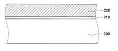
도 2a를 참조하면, 반도체 기판(200) 상에 실리콘 질화막(SiN)(210) 및 제1 마스크 층(220)이 형성된다. 상기 제1 마스크 층(220)은 다결정 실리콘층 또는 산화막으로 구성된다. 상기 반도체 기판(200)은 실리콘 단결정으로 이루어짐이 바람 직하다. 또한, 상기 제1 마스크 층(220)이 다결정 실리콘으로 이루어진 경우, 실리콘 질화막(210)의 상부에는 희생 산화막이 개재될 수 있다.Referring to FIG. 2A, a silicon nitride film (SiN) 210 and a
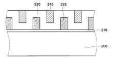
도 2b를 참조하면, 반도체 기판(200) 상에 실리콘 질화막(210)이 형성되고, 상기 실리콘 질화막(210) 상부에 제1 마스크 패턴(225)이 형성된다. 또한, 상기 제1 마스크 패턴(225) 및 노출된 실리콘 질화막(210) 상에는 증착층(230)이 형성된다.Referring to FIG. 2B, a
상기 도 2a의 제1 마스크층(220) 상부에 포토레지스트를 도포하고, 통상적인 포토리소그래피 공정을 이용하여 포토레지스트 패턴을 형성한다. 이어서, 포토레지스트 패턴이 형성된 반도체 기판(200)에 대해 건식 식각을 수행하고, 포토레지스트를 제거하면, 상기 제1 마스크 패턴(225)이 형성된다. 또한, 상기 제1 마스크 패턴(225) 및 노출된 실리콘 질화막(210) 상에 증착층(230)을 형성한다.A photoresist is applied on the
만일, 상기 제1 마스크 패턴(225)이 다결정 실리콘으로 이루어진 경우, 상기 증착층(230)은 산화물로 구성되며, 상기 제1 마스크 패턴(225)이 산화막인 경우, 상기 증착층(230)은 다결정 실리콘으로 이루어진다.If the
상기 제1 마스크 패턴(225)의 폭 W1'은 상기 제1 마스크 패턴(225)의 피치(pitch) P2의 1/4임이 바람직하다. 또한, 증착층(230)의 측벽들 사이의 거리 W2'는 제1 마스크 패턴(225)의 피치(pitch) P2의 1/4임이 바람직하다.The width W1 ′ of the
도 2c를 참조하면, 반도체 기판(200) 상에 실리콘 질화막(210), 제1 마스크 패턴(225) 및 증착층(230)이 형성되고, 증착층(230) 상에는 제2 마스크층(240)이 형성된다.Referring to FIG. 2C, a
상기 제2 마스크층(240)은 상기 제1 마스크 패턴(225)와 동일한 식각 선택비를 가진다. 바람직하게는 상기 제2 마스크층(240)과 상기 제1 마스크 패턴(225)은 동일한 물질로 이루어진다. 즉, 제1 마스크 패턴(225)이 다결정 실리콘으로 이루어진 경우, 상기 제2 마스크층(240)은 다결정 실리콘으로 이루어지며, 상기 제1 마스크 패턴(225)이 산화물로 구성된 경우, 상기 제2 마스크층(240)은 산화물로 이루어진다.The
도 2d를 참조하면, 반도체 기판(200) 상에 실리콘 질화막(210), 제1 마스크 패턴(225), 증착층(230) 및 증착층(230)의 측벽들 사이의 이격 공간에 매립된 제2 마스크 패턴(245)이 도시된다.Referring to FIG. 2D, a second buried in the spaced space between the
상기 제2 마스크 패턴(245)의 형성은 상기 도 2c의 제2 마스크층(240)에 대해 화학적 기계적 연마 또는 에치백 공정을 수행하여 상기 증착층(230) 상부의 제2 마스크층(240)을 제거하여 이루어진다. 따라서, 상기 증착층(230) 상부의 제2 마스크층(240)은 제거되고, 증착층(230)의 측벽들 사이의 이격 공간에는 제2 마스크 패턴(245)만이 잔류하게 된다.The
도 2e를 참조하면, 반도체 기판(200) 상에 실리콘 질화막(210), 제1 마스크 패턴(225), 증착층 패턴(235) 및 제2 마스크 패턴(245)이 도시된다. 상기 증착층 패턴(235)은 상기 도 2d에서 제1 마스크 패턴(225) 및 제2 마스크 패턴(245)을 식각 마스크로 하여 이방성 건식 식각에 의해 형성된다. 또한, 이방성 건식 식각이 수행되는 경우, 상기 실리콘 질화막(210)은 식각 저지막이 된다.Referring to FIG. 2E, a
이방성 건식 식각에 의해 상기 제2 마스크 패턴(245)의 하부에 도포된 증착 층(230)은 잔류하여 증착층 패턴(235)으로 형성된다. 또한, 상기 식각에 의해 제2 마스크 패턴(245) 사이의 증착층(230)은 제거되고, 하부의 실리콘 질화막(210)이 노출된다. 또한, 상기 제2 마스크 패턴(245)은 증착층(230)에 대해 식각 선택비를 가지므로 건식 식각이 수행되더라도 식각되지 않고 잔류한다. 마찬가지로, 제1 마스크 패턴(225)도 증착층(230)에 대해 식각 선택비를 가지므로 식각에도 불구하고 잔류하게 된다. 즉, 제1 마스크 패턴(225) 및 제2 마스크 패턴(245)은 증착층(230)의 식각에 대해 식각 마스크로서 기능한다.The
상기 제1 마스크 패턴(225) 및 제2 마스크 패턴(245)이 다결정 실리콘이고, 상기 증착층(230)이 산화물인 경우, 식각에 사용되는 식각 가스는 CHF3 또는 CH2F2 등이 사용된다. 또한, 상기 제1 마스크 패턴(225) 및 제2 마스크 패턴(245)이 산화물이고, 상기 증착층(230)이 다결정 실리콘인 경우, 식각에 사용되는 식각 가스는 Cl2, O2또는 Ar 등이 사용된다.When the
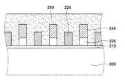
도 2f를 참조하면, 실리콘 질화막(210), 제1 마스크 패턴(225), 증착층 패턴(235) 및 제2 마스크 패턴(245)을 매립하는 유기 희생막(250)이 도시된다. 상기 유기 희생막(250)은 유기물로 이루어진다. 즉, 상기 유기 희생막(250)은 ArF 레이저, KrF 레이저 또는 I-line의 광원에 사용되는 포토레지스트일 수 있다. 이외에도 반사 방지막(Anti Reflective Coating) 또는 비정질 탄소막(Amorphous Carbon Layer) 등이 유기 희생막(250)으로 사용될 수 있다. 바람직하게는 상기 유기 희생막(250)은 스핀 코팅에 의해 형성되며, 실시의 형태에 따라 증착 공정에 의해서도 형성될 수 있다.Referring to FIG. 2F, an organic
이어서, 상기 유기 희생막(250)에 대해 화학적 기계적 연마 또는 에치백 공정을 수행하여 제1 마스크 패턴(225) 및 제2 마스크 패턴(245)에 대한 평탄화 공정을 수행한다. 평탄화 공정이 완료되면 평탄화된 제1 마스크 패턴(225)의 상부 표면 및 평탄화된 제2 마스크 패턴(245)의 상부 표면은 상기 실리콘 질화막(210) 표면으로부터 실질적으로 동일한 높이를 가진다.Subsequently, a chemical mechanical polishing or etch back process is performed on the organic
계속해서, 평탄화된 제1 마스크 패턴(225) 및 제2 마스크 패턴(245) 사이에 잔류하는 유기 희생막(250)은 에슁 공정에 의하여 제거된다.Subsequently, the organic
도 2g를 참조하면, 에슁 공정에 의해 유기 희생막(250)은 완전히 제거되고, 반도체 기판(200) 상에 실리콘 질화막(210), 제1 마스크 패턴(225), 증착층 패턴(235) 및 제2 마스크 패턴(245)이 도시된다. 특히, 평탄화 공정에 의해 제1 마스크 패턴(225)의 상부 표면과 제2 마스크 패턴(245)의 상부 표면을 동일 레벨의 높이를 가진다.Referring to FIG. 2G, the organic
도 2h를 참조하면, 상기 제1 마스크 패턴(225) 및 제2 마스크 패턴(245)을 식각 마스크로 하여 실리콘 질화막(210) 및 반도체 기판(200)을 식각하여 트렌치(260)를 형성한다.Referring to FIG. 2H, the
제1 마스크 패턴(225) 및 제2 마스크 패턴(245)의 높이는 동일하므로, 인접한 마스크 패턴들 사이의 높이의 차이에서 발생되는 로딩 효과(Loading effect)는 방지된다. 즉, 이방성 식각에 의해 형성되는 트렌치들은 서로 균일한 프로파일을 가질 수 있다.Since the heights of the
또한, 포토레지스트 공정에 의해 형성된 제1 마스크 패턴과는 달리 제2 마스크 패턴은 증착층 및 제2 마스크층의 형성에 의해 인접한 제1 마스크 패턴들 사이에 형성된다.In addition, unlike the first mask pattern formed by the photoresist process, the second mask pattern is formed between adjacent first mask patterns by formation of the deposition layer and the second mask layer.
특히 제1 마스크 패턴들 사이의 간격이 한계 해상도에 근접한 경우, 제1 마스크 패턴들 사이에는 제2 마스크 패턴들이 형성되므로 한계 해상도에 비해 2배의 집적도를 가진 트렌치를 얻을 수 있다.In particular, when the distance between the first mask patterns is close to the limit resolution, since the second mask patterns are formed between the first mask patterns, a trench having an integration density twice as large as the limit resolution may be obtained.
상기와 같은 본 발명에 따르면, 하지막 패턴 또는 트렌치의 형성시, 자기정렬 이중 패터닝에 의해 형성된 마스크 패턴들은 동일한 높이를 가진다. 따라서, 하지막 또는 반도체 기판에 대해 식각을 수행하는 경우, 마스크 패턴들의 높이의 불균일에 의해 발생되는 로딩 효과는 방지된다.According to the present invention as described above, in the formation of the underlying film pattern or trench, the mask patterns formed by self-aligned double patterning have the same height. Therefore, when etching is performed on the underlying film or the semiconductor substrate, the loading effect caused by the unevenness of the height of the mask patterns is prevented.
또한, 한계해상도에 근접한 피치를 가지는 패턴들 사이에 자기정렬된 패턴을 형성할 수 있으므로 2배의 집적도를 가진 하지막 패턴 또는 트렌치를 형성할 수 있다.In addition, since a self-aligned pattern can be formed between patterns having a pitch close to the limit resolution, an underlayer pattern or a trench having a double density can be formed.
상기에서는 본 발명의 바람직한 실시예를 참조하여 설명하였지만, 해당 기술 분야의 숙련된 당업자는 하기의 특허 청구의 범위에 기재된 본 발명의 사상 및 영역으로부터 벗어나지 않는 범위 내에서 본 발명을 다양하게 수정 및 변경시킬 수 있음을 이해할 수 있을 것이다.Although described above with reference to a preferred embodiment of the present invention, those skilled in the art will be variously modified and changed within the scope of the invention without departing from the spirit and scope of the invention described in the claims below I can understand that you can.
Claims (18)
Translated fromKoreanPriority Applications (2)
| Application Number | Priority Date | Filing Date | Title |
|---|---|---|---|
| KR1020050129928AKR100714305B1 (en) | 2005-12-26 | 2005-12-26 | Formation method of self-aligned double pattern |
| US11/602,270US7531456B2 (en) | 2005-12-26 | 2006-11-21 | Method of forming self-aligned double pattern |
Applications Claiming Priority (1)
| Application Number | Priority Date | Filing Date | Title |
|---|---|---|---|
| KR1020050129928AKR100714305B1 (en) | 2005-12-26 | 2005-12-26 | Formation method of self-aligned double pattern |
Publications (1)
| Publication Number | Publication Date |
|---|---|
| KR100714305B1true KR100714305B1 (en) | 2007-05-02 |
Family
ID=38194429
Family Applications (1)
| Application Number | Title | Priority Date | Filing Date |
|---|---|---|---|
| KR1020050129928AActiveKR100714305B1 (en) | 2005-12-26 | 2005-12-26 | Formation method of self-aligned double pattern |
Country Status (2)
| Country | Link |
|---|---|
| US (1) | US7531456B2 (en) |
| KR (1) | KR100714305B1 (en) |
Cited By (14)
| Publication number | Priority date | Publication date | Assignee | Title |
|---|---|---|---|---|
| KR100817088B1 (en) | 2007-02-16 | 2008-03-26 | 삼성전자주식회사 | Method of forming fine metal wiring pattern of semiconductor device using damascene process |
| KR100818387B1 (en)* | 2006-08-31 | 2008-04-01 | 동부일렉트로닉스 주식회사 | Metal wiring formation method of semiconductor device |
| KR100818389B1 (en)* | 2006-08-31 | 2008-04-01 | 동부일렉트로닉스 주식회사 | Method of forming fine pattern of semiconductor device |
| KR100858877B1 (en) | 2007-08-13 | 2008-09-17 | 주식회사 하이닉스반도체 | Semiconductor device manufacturing method |
| KR100866735B1 (en) | 2007-05-01 | 2008-11-03 | 주식회사 하이닉스반도체 | Method of forming fine pattern of semiconductor device |
| KR100919564B1 (en)* | 2007-06-29 | 2009-10-01 | 주식회사 하이닉스반도체 | Method for Forming Fine Pattern of Semiconductor Device |
| KR100929302B1 (en)* | 2007-12-26 | 2009-11-27 | 주식회사 하이닉스반도체 | Pattern formation method of semiconductor device |
| KR100939168B1 (en) | 2008-02-28 | 2010-01-28 | 주식회사 하이닉스반도체 | Pattern formation method of semiconductor device |
| KR100942078B1 (en)* | 2007-12-27 | 2010-02-12 | 주식회사 하이닉스반도체 | Method of forming fine pattern of semiconductor device |
| KR100942075B1 (en) | 2007-12-27 | 2010-02-12 | 주식회사 하이닉스반도체 | Method of forming fine pattern of semiconductor device |
| US7977204B2 (en) | 2008-12-15 | 2011-07-12 | Samsung Electronics Co., Ltd. | Method of forming a fine pattern of a semiconductor device using a double patterning technique |
| WO2013032873A1 (en)* | 2011-08-26 | 2013-03-07 | Applied Materials, Inc. | Double patterning etching process |
| KR101529867B1 (en)* | 2008-10-27 | 2015-06-18 | 삼성전자주식회사 | Embedded type gate electrode using self-aligned dual patterning technology and semiconductor having device isolation film and method for manufacturing the same |
| CN118870807A (en)* | 2023-04-23 | 2024-10-29 | 长鑫存储技术有限公司 | Method for preparing semiconductor structure |
Families Citing this family (94)
| Publication number | Priority date | Publication date | Assignee | Title |
|---|---|---|---|---|
| US7355384B2 (en)* | 2004-04-08 | 2008-04-08 | International Business Machines Corporation | Apparatus, method, and computer program product for monitoring and controlling a microcomputer using a single existing pin |
| US7910288B2 (en) | 2004-09-01 | 2011-03-22 | Micron Technology, Inc. | Mask material conversion |
| US7611944B2 (en) | 2005-03-28 | 2009-11-03 | Micron Technology, Inc. | Integrated circuit fabrication |
| KR100640640B1 (en)* | 2005-04-19 | 2006-10-31 | 삼성전자주식회사 | Fine Pattern Forming Method of Semiconductor Device Using Fine Pitch Hard Mask |
| US7429536B2 (en) | 2005-05-23 | 2008-09-30 | Micron Technology, Inc. | Methods for forming arrays of small, closely spaced features |
| US7560390B2 (en) | 2005-06-02 | 2009-07-14 | Micron Technology, Inc. | Multiple spacer steps for pitch multiplication |
| US7393789B2 (en) | 2005-09-01 | 2008-07-01 | Micron Technology, Inc. | Protective coating for planarization |
| US7572572B2 (en) | 2005-09-01 | 2009-08-11 | Micron Technology, Inc. | Methods for forming arrays of small, closely spaced features |
| US7897058B2 (en)* | 2006-02-13 | 2011-03-01 | Asml Netherlands B.V. | Device manufacturing method and computer program product |
| US7767570B2 (en)* | 2006-03-22 | 2010-08-03 | Taiwan Semiconductor Manufacturing Company, Ltd. | Dummy vias for damascene process |
| US7902074B2 (en) | 2006-04-07 | 2011-03-08 | Micron Technology, Inc. | Simplified pitch doubling process flow |
| US7488685B2 (en) | 2006-04-25 | 2009-02-10 | Micron Technology, Inc. | Process for improving critical dimension uniformity of integrated circuit arrays |
| US7611980B2 (en) | 2006-08-30 | 2009-11-03 | Micron Technology, Inc. | Single spacer process for multiplying pitch by a factor greater than two and related intermediate IC structures |
| US7666578B2 (en) | 2006-09-14 | 2010-02-23 | Micron Technology, Inc. | Efficient pitch multiplication process |
| US7923373B2 (en) | 2007-06-04 | 2011-04-12 | Micron Technology, Inc. | Pitch multiplication using self-assembling materials |
| US8563229B2 (en) | 2007-07-31 | 2013-10-22 | Micron Technology, Inc. | Process of semiconductor fabrication with mask overlay on pitch multiplied features and associated structures |
| US7919413B2 (en)* | 2007-08-06 | 2011-04-05 | Industrial Technology Research Institute | Methods for forming patterns |
| US7659208B2 (en) | 2007-12-06 | 2010-02-09 | Micron Technology, Inc | Method for forming high density patterns |
| US7790531B2 (en) | 2007-12-18 | 2010-09-07 | Micron Technology, Inc. | Methods for isolating portions of a loop of pitch-multiplied material and related structures |
| CN101971291B (en)* | 2008-02-08 | 2013-04-03 | 朗姆研究公司 | Double mask self-aligned double patterning technology (SaDPT) process |
| JP5254049B2 (en)* | 2008-02-15 | 2013-08-07 | 東京エレクトロン株式会社 | Pattern forming method and semiconductor device manufacturing method |
| JP5086283B2 (en)* | 2008-02-15 | 2012-11-28 | 東京エレクトロン株式会社 | Pattern forming method and semiconductor device manufacturing method |
| US8030218B2 (en) | 2008-03-21 | 2011-10-04 | Micron Technology, Inc. | Method for selectively modifying spacing between pitch multiplied structures |
| US7935965B1 (en) | 2008-05-16 | 2011-05-03 | Pdf Solutions, Inc. | Test structures and methods for electrical characterization of alignment of line patterns defined with double patterning |
| JP2009289974A (en)* | 2008-05-29 | 2009-12-10 | Toshiba Corp | Method of manufacturing semiconductor device |
| JP2010080942A (en)* | 2008-08-25 | 2010-04-08 | Elpida Memory Inc | Method of manufacturing semiconductor device |
| US8492282B2 (en)* | 2008-11-24 | 2013-07-23 | Micron Technology, Inc. | Methods of forming a masking pattern for integrated circuits |
| US7972959B2 (en)* | 2008-12-01 | 2011-07-05 | Applied Materials, Inc. | Self aligned double patterning flow with non-sacrificial features |
| US8133664B2 (en)* | 2009-03-03 | 2012-03-13 | Micron Technology, Inc. | Methods of forming patterns |
| US8519540B2 (en)* | 2009-06-16 | 2013-08-27 | International Business Machines Corporation | Self-aligned dual damascene BEOL structures with patternable low- K material and methods of forming same |
| US8659115B2 (en)* | 2009-06-17 | 2014-02-25 | International Business Machines Corporation | Airgap-containing interconnect structure with improved patternable low-K material and method of fabricating |
| US8163658B2 (en)* | 2009-08-24 | 2012-04-24 | International Business Machines Corporation | Multiple patterning using improved patternable low-k dielectric materials |
| US8202783B2 (en) | 2009-09-29 | 2012-06-19 | International Business Machines Corporation | Patternable low-k dielectric interconnect structure with a graded cap layer and method of fabrication |
| US8394280B1 (en) | 2009-11-06 | 2013-03-12 | Western Digital (Fremont), Llc | Resist pattern protection technique for double patterning application |
| US8637395B2 (en)* | 2009-11-16 | 2014-01-28 | International Business Machines Corporation | Methods for photo-patternable low-k (PPLK) integration with curing after pattern transfer |
| US8367540B2 (en)* | 2009-11-19 | 2013-02-05 | International Business Machines Corporation | Interconnect structure including a modified photoresist as a permanent interconnect dielectric and method of fabricating same |
| KR20110095694A (en)* | 2010-02-19 | 2011-08-25 | 삼성전자주식회사 | How to form a pattern structure |
| US8642252B2 (en) | 2010-03-10 | 2014-02-04 | International Business Machines Corporation | Methods for fabrication of an air gap-containing interconnect structure |
| US8896120B2 (en) | 2010-04-27 | 2014-11-25 | International Business Machines Corporation | Structures and methods for air gap integration |
| US8241992B2 (en) | 2010-05-10 | 2012-08-14 | International Business Machines Corporation | Method for air gap interconnect integration using photo-patternable low k material |
| US8373271B2 (en) | 2010-05-27 | 2013-02-12 | International Business Machines Corporation | Interconnect structure with an oxygen-doped SiC antireflective coating and method of fabrication |
| US8563439B2 (en)* | 2010-07-23 | 2013-10-22 | Taiwan Semiconductor Manufacturing Company, Ltd. | Method of pitch dimension shrinkage |
| US8461038B2 (en)* | 2011-03-02 | 2013-06-11 | Texas Instruments Incorporated | Two-track cross-connects in double-patterned metal layers using a forbidden zone |
| US8575020B2 (en)* | 2011-03-02 | 2013-11-05 | Texas Instruments Incorporated | Pattern-split decomposition strategy for double-patterned lithography process |
| US8309462B1 (en) | 2011-09-29 | 2012-11-13 | Sandisk Technologies Inc. | Double spacer quadruple patterning with self-connected hook-up |
| US8946078B2 (en)* | 2012-03-22 | 2015-02-03 | United Microelectronics Corp. | Method of forming trench in semiconductor substrate |
| CN103594337B (en)* | 2012-08-14 | 2016-05-25 | 中芯国际集成电路制造(上海)有限公司 | Double-patterning method |
| US9177820B2 (en) | 2012-10-24 | 2015-11-03 | Globalfoundries U.S. 2 Llc | Sub-lithographic semiconductor structures with non-constant pitch |
| CN103794476B (en)* | 2012-10-30 | 2017-09-22 | 中芯国际集成电路制造(上海)有限公司 | The forming method of the triple figures of autoregistration |
| US9318330B2 (en)* | 2012-12-27 | 2016-04-19 | Renesas Electronics Corporation | Patterning process method for semiconductor devices |
| CN103928392B (en)* | 2013-01-10 | 2017-05-17 | 中芯国际集成电路制造(上海)有限公司 | Manufacturing method of local interconnection structure |
| US9406331B1 (en) | 2013-06-17 | 2016-08-02 | Western Digital (Fremont), Llc | Method for making ultra-narrow read sensor and read transducer device resulting therefrom |
| US9564361B2 (en) | 2013-09-13 | 2017-02-07 | Qualcomm Incorporated | Reverse self aligned double patterning process for back end of line fabrication of a semiconductor device |
| US9230809B2 (en)* | 2013-10-17 | 2016-01-05 | Taiwan Semiconductor Manufacturing Company, Ltd. | Self-aligned double patterning |
| US9159577B2 (en)* | 2014-02-14 | 2015-10-13 | Taiwan Semiconductor Manufacturing Company Limited | Method of forming substrate pattern |
| KR101860251B1 (en)* | 2014-02-23 | 2018-05-21 | 도쿄엘렉트론가부시키가이샤 | Method for patterning a substrate for planarization |
| TWI545622B (en) | 2014-02-23 | 2016-08-11 | 東京威力科創股份有限公司 | Method for multiplying pattern density by crossing multiple patterned layers |
| US9640397B2 (en)* | 2014-03-14 | 2017-05-02 | Taiwan Semiconductor Manufacturing Company, Ltd. | Method of fabricating a semiconductor integrated circuit using a directed self-assembly block copolymer |
| CN103928313B (en)* | 2014-04-22 | 2017-12-15 | 上海华力微电子有限公司 | A kind of preparation method of small size figure |
| CN105336571B (en)* | 2014-07-28 | 2018-06-01 | 中芯国际集成电路制造(上海)有限公司 | The forming method of autoregistration multiple graphics mask |
| US9564312B2 (en) | 2014-11-24 | 2017-02-07 | Lam Research Corporation | Selective inhibition in atomic layer deposition of silicon-containing films |
| US9312064B1 (en) | 2015-03-02 | 2016-04-12 | Western Digital (Fremont), Llc | Method to fabricate a magnetic head including ion milling of read gap using dual layer hard mask |
| TWI640042B (en)* | 2015-03-09 | 2018-11-01 | 聯華電子股份有限公司 | Manufacturing method of patterned structure of semiconductor device |
| US10061210B2 (en)* | 2015-07-31 | 2018-08-28 | Nanometrics Incorporated | 3D target for monitoring multiple patterning process |
| KR102398664B1 (en) | 2016-01-26 | 2022-05-16 | 삼성전자주식회사 | Method of manufacturing semiconductor device |
| US10483073B2 (en) | 2016-03-14 | 2019-11-19 | Elwha Llc | Fabrication of vacuum electronic components with self-aligned double patterning lithography |
| US10629435B2 (en) | 2016-07-29 | 2020-04-21 | Lam Research Corporation | Doped ALD films for semiconductor patterning applications |
| US10832908B2 (en)* | 2016-11-11 | 2020-11-10 | Lam Research Corporation | Self-aligned multi-patterning process flow with ALD gapfill spacer mask |
| CN108091553B (en)* | 2016-11-23 | 2020-10-09 | 中芯国际集成电路制造(北京)有限公司 | Method for forming mask pattern |
| CN108389830B (en)* | 2017-02-03 | 2020-10-16 | 联华电子股份有限公司 | Method for manufacturing mask |
| CN108574010B (en)* | 2017-03-08 | 2021-05-04 | 中芯国际集成电路制造(上海)有限公司 | Semiconductor structure and method of forming the same |
| CN108054085B (en)* | 2017-03-30 | 2019-03-12 | 长鑫存储技术有限公司 | The preparation method of memory |
| CN109427686B (en) | 2017-08-29 | 2021-04-13 | 联华电子股份有限公司 | Isolation structure and method of forming the same |
| US10269559B2 (en) | 2017-09-13 | 2019-04-23 | Lam Research Corporation | Dielectric gapfill of high aspect ratio features utilizing a sacrificial etch cap layer |
| US10147608B1 (en)* | 2017-11-09 | 2018-12-04 | Nanya Technology Corporation | Method for preparing a patterned target layer |
| CN112005343B (en) | 2018-03-02 | 2025-05-06 | 朗姆研究公司 | Selective deposition using hydrolysis |
| CN110391133B (en) | 2018-04-17 | 2021-07-20 | 联华电子股份有限公司 | patterning method |
| US10475648B1 (en)* | 2018-05-01 | 2019-11-12 | United Microelectronics Corp. | Method for patterning a semiconductor structure |
| CN110544688B (en)* | 2018-05-29 | 2024-12-06 | 长鑫存储技术有限公司 | Active array, method for manufacturing active array and random access memory |
| CN108847387A (en)* | 2018-06-22 | 2018-11-20 | 长江存储科技有限责任公司 | A kind of hole forming method |
| US10643846B2 (en) | 2018-06-28 | 2020-05-05 | Lam Research Corporation | Selective growth of metal-containing hardmask thin films |
| KR102837863B1 (en) | 2019-06-04 | 2025-07-23 | 램 리써치 코포레이션 | Polymeric protective liner for reactive ion etching during patterning |
| CN114207184A (en) | 2019-08-06 | 2022-03-18 | 朗姆研究公司 | Thermal Atomic Layer Deposition of Silicon-Containing Films |
| CN113921472B (en)* | 2020-07-08 | 2024-07-19 | 长鑫存储技术有限公司 | Semiconductor structure and manufacturing method thereof |
| CN115735261A (en) | 2020-07-28 | 2023-03-03 | 朗姆研究公司 | Impurity reduction in silicon-containing films |
| CN114446769B (en)* | 2020-11-06 | 2024-09-13 | 长鑫存储技术有限公司 | Method for preparing semiconductor device |
| US12278106B2 (en) | 2020-11-06 | 2025-04-15 | Changxin Memory Technologies, Inc. | Preparation method of semiconductor device |
| CN115548086A (en) | 2021-06-29 | 2022-12-30 | 联华电子股份有限公司 | Manufacturing method of semiconductor element |
| CN115565979A (en) | 2021-07-02 | 2023-01-03 | 长鑫存储技术有限公司 | A kind of semiconductor transistor structure and manufacturing method |
| US11972977B2 (en) | 2021-09-08 | 2024-04-30 | International Business Machines Corporation | Fabrication of rigid close-pitch interconnects |
| KR20230163051A (en)* | 2022-05-23 | 2023-11-30 | 삼성전자주식회사 | Mathod for manufacturing semiconductor device |
| US11830744B1 (en) | 2022-05-31 | 2023-11-28 | Nanya Technology Corporation | Method of preparing active areas |
| US20230411162A1 (en)* | 2022-06-16 | 2023-12-21 | Nanya Technology Corporation | Method of manufacturing semiconductor structure |
| CN118299254B (en)* | 2024-06-05 | 2024-09-27 | 汉轩微电子制造(江苏)有限公司 | Semiconductor device and method for manufacturing the same |
Citations (3)
| Publication number | Priority date | Publication date | Assignee | Title |
|---|---|---|---|---|
| KR20000004547A (en)* | 1998-06-30 | 2000-01-25 | 김영환 | Method for forming fine pattern of semiconductor device |
| JP2001085510A (en) | 1999-09-14 | 2001-03-30 | Toshiba Corp | Method for manufacturing semiconductor device |
| KR20040057532A (en)* | 2002-12-26 | 2004-07-02 | 주식회사 하이닉스반도체 | Method for fabrication of semiconductor device using ArF photo-lithography capable of protecting tapered profile of hardmask |
Family Cites Families (10)
| Publication number | Priority date | Publication date | Assignee | Title |
|---|---|---|---|---|
| KR100281891B1 (en) | 1994-11-30 | 2001-04-02 | 윤종용 | Wiring pattern formation method of semiconductor device |
| KR0165399B1 (en) | 1995-05-29 | 1999-02-01 | 김광호 | Fine pattern formation method |
| US6063688A (en)* | 1997-09-29 | 2000-05-16 | Intel Corporation | Fabrication of deep submicron structures and quantum wire transistors using hard-mask transistor width definition |
| US6638441B2 (en) | 2002-01-07 | 2003-10-28 | Macronix International Co., Ltd. | Method for pitch reduction |
| KR100489657B1 (en)* | 2003-02-21 | 2005-05-17 | 삼성전자주식회사 | Method for forming patterns in a semiconductor device and method for a semiconductor device using the same |
| KR100541046B1 (en)* | 2003-05-27 | 2006-01-11 | 삼성전자주식회사 | How to form a self-aligned contact structure using a sacrificial mask film |
| US7183142B2 (en)* | 2005-01-13 | 2007-02-27 | International Business Machines Corporation | FinFETs with long gate length at high density |
| US7560388B2 (en)* | 2005-11-30 | 2009-07-14 | Lam Research Corporation | Self-aligned pitch reduction |
| KR100829606B1 (en)* | 2006-09-07 | 2008-05-14 | 삼성전자주식회사 | How to form a fine pattern |
| KR100790998B1 (en)* | 2006-10-02 | 2008-01-03 | 삼성전자주식회사 | Pad pattern formation method using self-aligned double patterning method and contact hole formation method using self-aligned double patterning method |
- 2005
- 2005-12-26KRKR1020050129928Apatent/KR100714305B1/enactiveActive
- 2006
- 2006-11-21USUS11/602,270patent/US7531456B2/enactiveActive
Patent Citations (3)
| Publication number | Priority date | Publication date | Assignee | Title |
|---|---|---|---|---|
| KR20000004547A (en)* | 1998-06-30 | 2000-01-25 | 김영환 | Method for forming fine pattern of semiconductor device |
| JP2001085510A (en) | 1999-09-14 | 2001-03-30 | Toshiba Corp | Method for manufacturing semiconductor device |
| KR20040057532A (en)* | 2002-12-26 | 2004-07-02 | 주식회사 하이닉스반도체 | Method for fabrication of semiconductor device using ArF photo-lithography capable of protecting tapered profile of hardmask |
Cited By (19)
| Publication number | Priority date | Publication date | Assignee | Title |
|---|---|---|---|---|
| KR100818387B1 (en)* | 2006-08-31 | 2008-04-01 | 동부일렉트로닉스 주식회사 | Metal wiring formation method of semiconductor device |
| KR100818389B1 (en)* | 2006-08-31 | 2008-04-01 | 동부일렉트로닉스 주식회사 | Method of forming fine pattern of semiconductor device |
| KR100817088B1 (en) | 2007-02-16 | 2008-03-26 | 삼성전자주식회사 | Method of forming fine metal wiring pattern of semiconductor device using damascene process |
| KR100866735B1 (en) | 2007-05-01 | 2008-11-03 | 주식회사 하이닉스반도체 | Method of forming fine pattern of semiconductor device |
| US7972766B2 (en) | 2007-06-29 | 2011-07-05 | Hynix Semiconductor Inc. | Method for forming fine pattern of semiconductor device |
| KR100919564B1 (en)* | 2007-06-29 | 2009-10-01 | 주식회사 하이닉스반도체 | Method for Forming Fine Pattern of Semiconductor Device |
| KR100858877B1 (en) | 2007-08-13 | 2008-09-17 | 주식회사 하이닉스반도체 | Semiconductor device manufacturing method |
| KR100929302B1 (en)* | 2007-12-26 | 2009-11-27 | 주식회사 하이닉스반도체 | Pattern formation method of semiconductor device |
| US8143163B2 (en) | 2007-12-26 | 2012-03-27 | Hynix Semiconductor Inc. | Method for forming pattern of semiconductor device |
| KR100942078B1 (en)* | 2007-12-27 | 2010-02-12 | 주식회사 하이닉스반도체 | Method of forming fine pattern of semiconductor device |
| US7879729B2 (en) | 2007-12-27 | 2011-02-01 | Hynix Semiconductor Inc. | Method of forming a micro pattern of a semiconductor device |
| KR100942075B1 (en) | 2007-12-27 | 2010-02-12 | 주식회사 하이닉스반도체 | Method of forming fine pattern of semiconductor device |
| US8647521B2 (en) | 2007-12-27 | 2014-02-11 | SK Hynix Inc. | Method of forming micro pattern of semiconductor device |
| KR100939168B1 (en) | 2008-02-28 | 2010-01-28 | 주식회사 하이닉스반도체 | Pattern formation method of semiconductor device |
| KR101529867B1 (en)* | 2008-10-27 | 2015-06-18 | 삼성전자주식회사 | Embedded type gate electrode using self-aligned dual patterning technology and semiconductor having device isolation film and method for manufacturing the same |
| US7977204B2 (en) | 2008-12-15 | 2011-07-12 | Samsung Electronics Co., Ltd. | Method of forming a fine pattern of a semiconductor device using a double patterning technique |
| WO2013032873A1 (en)* | 2011-08-26 | 2013-03-07 | Applied Materials, Inc. | Double patterning etching process |
| US8759223B2 (en) | 2011-08-26 | 2014-06-24 | Applied Materials, Inc. | Double patterning etching process |
| CN118870807A (en)* | 2023-04-23 | 2024-10-29 | 长鑫存储技术有限公司 | Method for preparing semiconductor structure |
Also Published As
| Publication number | Publication date |
|---|---|
| US7531456B2 (en) | 2009-05-12 |
| US20070148968A1 (en) | 2007-06-28 |
Similar Documents
| Publication | Publication Date | Title |
|---|---|---|
| KR100714305B1 (en) | Formation method of self-aligned double pattern | |
| US6955961B1 (en) | Method for defining a minimum pitch in an integrated circuit beyond photolithographic resolution | |
| KR100858877B1 (en) | Semiconductor device manufacturing method | |
| KR20150101398A (en) | A method for producing fin structures of a semiconductor device in a substrate | |
| CN110690117A (en) | Semiconductor structure and method of forming the same | |
| KR100810895B1 (en) | Semiconductor device and manufacturing method | |
| US20110248385A1 (en) | Method for selectively forming symmetrical or asymmetrical features using a symmetrical photomask during fabrication of a semiconductor device and electronic systems including the semiconductor device | |
| TW200828502A (en) | Method for fabricating landing plug contact in semiconductor device | |
| US20100055922A1 (en) | Method for fabricating semiconductor device | |
| JP4095588B2 (en) | Method for defining a minimum pitch that exceeds photolithographic resolution in an integrated circuit | |
| KR100726148B1 (en) | Manufacturing method of semiconductor device | |
| KR100650859B1 (en) | Method of forming fine pattern of semiconductor device | |
| KR100912958B1 (en) | Manufacturing method of fine pattern of semiconductor device | |
| KR101016855B1 (en) | Dual damascene pattern formation method of semiconductor device | |
| KR100460718B1 (en) | Method for manufacturing metal insulator metal capacitor | |
| KR100356478B1 (en) | Method of forming a gate electrode in a semiconductor device | |
| KR100772077B1 (en) | Contact hole formation method of semiconductor device | |
| KR100561513B1 (en) | Shallow trench isolation method for semiconductor devices | |
| KR100413043B1 (en) | Gate electrode formation method of semiconductor device | |
| KR100602133B1 (en) | Method of forming mask pattern of semiconductor device | |
| KR100632071B1 (en) | Metal wiring formation method of semiconductor device | |
| KR20080088929A (en) | Semiconductor device manufacturing method | |
| KR20120055153A (en) | Method for fabricating semiconductor device | |
| KR20000045440A (en) | Method for forming contact of semiconductor device | |
| KR20050073363A (en) | Method of forming a contact hole in a semiconductor device |
Legal Events
| Date | Code | Title | Description |
|---|---|---|---|
| A201 | Request for examination | ||
| PA0109 | Patent application | Patent event code:PA01091R01D Comment text:Patent Application Patent event date:20051226 | |
| PA0201 | Request for examination | ||
| E902 | Notification of reason for refusal | ||
| PE0902 | Notice of grounds for rejection | Comment text:Notification of reason for refusal Patent event date:20061117 Patent event code:PE09021S01D | |
| E701 | Decision to grant or registration of patent right | ||
| PE0701 | Decision of registration | Patent event code:PE07011S01D Comment text:Decision to Grant Registration Patent event date:20070312 | |
| GRNT | Written decision to grant | ||
| PR0701 | Registration of establishment | Comment text:Registration of Establishment Patent event date:20070426 Patent event code:PR07011E01D | |
| PR1002 | Payment of registration fee | Payment date:20070427 End annual number:3 Start annual number:1 | |
| PG1601 | Publication of registration | ||
| PR1001 | Payment of annual fee | Payment date:20100413 Start annual number:4 End annual number:4 | |
| PR1001 | Payment of annual fee | Payment date:20110405 Start annual number:5 End annual number:5 | |
| FPAY | Annual fee payment | ||
| PR1001 | Payment of annual fee | Payment date:20120402 Start annual number:6 End annual number:6 | |
| FPAY | Annual fee payment | ||
| PR1001 | Payment of annual fee | Payment date:20130329 Start annual number:7 End annual number:7 | |
| PR1001 | Payment of annual fee | Payment date:20140331 Start annual number:8 End annual number:8 | |
| PR1001 | Payment of annual fee | Payment date:20150331 Start annual number:9 End annual number:9 | |
| PR1001 | Payment of annual fee | Payment date:20160331 Start annual number:10 End annual number:10 | |
| PR1001 | Payment of annual fee | Payment date:20170331 Start annual number:11 End annual number:11 | |
| PR1001 | Payment of annual fee | Payment date:20180330 Start annual number:12 End annual number:12 | |
| FPAY | Annual fee payment | Payment date:20190329 Year of fee payment:13 | |
| PR1001 | Payment of annual fee | Payment date:20190329 Start annual number:13 End annual number:13 | |
| PR1001 | Payment of annual fee | Payment date:20200330 Start annual number:14 End annual number:14 | |
| PR1001 | Payment of annual fee | Payment date:20210329 Start annual number:15 End annual number:15 | |
| PR1001 | Payment of annual fee | Payment date:20220323 Start annual number:16 End annual number:16 | |
| PR1001 | Payment of annual fee | Payment date:20230327 Start annual number:17 End annual number:17 | |
| PR1001 | Payment of annual fee | Payment date:20240325 Start annual number:18 End annual number:18 |