KR100714010B1 - LED display device - Google Patents
LED display deviceDownload PDFInfo
- Publication number
- KR100714010B1 KR100714010B1KR1020050029185AKR20050029185AKR100714010B1KR 100714010 B1KR100714010 B1KR 100714010B1KR 1020050029185 AKR1020050029185 AKR 1020050029185AKR 20050029185 AKR20050029185 AKR 20050029185AKR 100714010 B1KR100714010 B1KR 100714010B1
- Authority
- KR
- South Korea
- Prior art keywords
- light emitting
- lower electrode
- electrode
- layer
- thin film
- Prior art date
- Legal status (The legal status is an assumption and is not a legal conclusion. Google has not performed a legal analysis and makes no representation as to the accuracy of the status listed.)
- Expired - Lifetime
Links
Images


Classifications
- H—ELECTRICITY
- H10—SEMICONDUCTOR DEVICES; ELECTRIC SOLID-STATE DEVICES NOT OTHERWISE PROVIDED FOR
- H10K—ORGANIC ELECTRIC SOLID-STATE DEVICES
- H10K59/00—Integrated devices, or assemblies of multiple devices, comprising at least one organic light-emitting element covered by group H10K50/00
- H10K59/10—OLED displays
- H10K59/12—Active-matrix OLED [AMOLED] displays
- H—ELECTRICITY
- H10—SEMICONDUCTOR DEVICES; ELECTRIC SOLID-STATE DEVICES NOT OTHERWISE PROVIDED FOR
- H10K—ORGANIC ELECTRIC SOLID-STATE DEVICES
- H10K59/00—Integrated devices, or assemblies of multiple devices, comprising at least one organic light-emitting element covered by group H10K50/00
- H10K59/80—Constructional details
- H10K59/805—Electrodes
- H10K59/8052—Cathodes
- H10K59/80522—Cathodes combined with auxiliary electrodes
- H—ELECTRICITY
- H10—SEMICONDUCTOR DEVICES; ELECTRIC SOLID-STATE DEVICES NOT OTHERWISE PROVIDED FOR
- H10K—ORGANIC ELECTRIC SOLID-STATE DEVICES
- H10K50/00—Organic light-emitting devices
- H10K50/80—Constructional details
- H10K50/805—Electrodes
- H—ELECTRICITY
- H10—SEMICONDUCTOR DEVICES; ELECTRIC SOLID-STATE DEVICES NOT OTHERWISE PROVIDED FOR
- H10K—ORGANIC ELECTRIC SOLID-STATE DEVICES
- H10K50/00—Organic light-emitting devices
- H10K50/80—Constructional details
- H10K50/805—Electrodes
- H10K50/81—Anodes
- H10K50/814—Anodes combined with auxiliary electrodes, e.g. ITO layer combined with metal lines
- H—ELECTRICITY
- H10—SEMICONDUCTOR DEVICES; ELECTRIC SOLID-STATE DEVICES NOT OTHERWISE PROVIDED FOR
- H10K—ORGANIC ELECTRIC SOLID-STATE DEVICES
- H10K50/00—Organic light-emitting devices
- H10K50/80—Constructional details
- H10K50/805—Electrodes
- H10K50/82—Cathodes
- H10K50/824—Cathodes combined with auxiliary electrodes
- H—ELECTRICITY
- H10—SEMICONDUCTOR DEVICES; ELECTRIC SOLID-STATE DEVICES NOT OTHERWISE PROVIDED FOR
- H10K—ORGANIC ELECTRIC SOLID-STATE DEVICES
- H10K59/00—Integrated devices, or assemblies of multiple devices, comprising at least one organic light-emitting element covered by group H10K50/00
- H10K59/10—OLED displays
- H10K59/12—Active-matrix OLED [AMOLED] displays
- H10K59/121—Active-matrix OLED [AMOLED] displays characterised by the geometry or disposition of pixel elements
- H10K59/1213—Active-matrix OLED [AMOLED] displays characterised by the geometry or disposition of pixel elements the pixel elements being TFTs
- H—ELECTRICITY
- H10—SEMICONDUCTOR DEVICES; ELECTRIC SOLID-STATE DEVICES NOT OTHERWISE PROVIDED FOR
- H10K—ORGANIC ELECTRIC SOLID-STATE DEVICES
- H10K59/00—Integrated devices, or assemblies of multiple devices, comprising at least one organic light-emitting element covered by group H10K50/00
- H10K59/10—OLED displays
- H10K59/12—Active-matrix OLED [AMOLED] displays
- H10K59/128—Active-matrix OLED [AMOLED] displays comprising two independent displays, e.g. for emitting information from two major sides of the display
- H—ELECTRICITY
- H01—ELECTRIC ELEMENTS
- H01L—SEMICONDUCTOR DEVICES NOT COVERED BY CLASS H10
- H01L2924/00—Indexing scheme for arrangements or methods for connecting or disconnecting semiconductor or solid-state bodies as covered by H01L24/00
- H01L2924/10—Details of semiconductor or other solid state devices to be connected
- H01L2924/11—Device type
- H01L2924/12—Passive devices, e.g. 2 terminal devices
- H01L2924/1204—Optical Diode
- H01L2924/12044—OLED
Landscapes
- Physics & Mathematics (AREA)
- Optics & Photonics (AREA)
- Engineering & Computer Science (AREA)
- Microelectronics & Electronic Packaging (AREA)
- Geometry (AREA)
- Electroluminescent Light Sources (AREA)
Abstract
Translated fromKoreanDescription
Translated fromKorean도 1은 종래의 양면발광 가능한 발광소자의 구조를 나타내는 개략적인 단면도이다.1 is a schematic cross-sectional view showing the structure of a conventional double-side light emitting device.
도 2는 본 발명에 따른 발광소자를 구현하는 화소회로를 나타내는 회로도이다.2 is a circuit diagram illustrating a pixel circuit implementing the light emitting device according to the present invention.
도 3은 본 발명의 일실시예에 따른 양면발광 가능한 발광소자가 채용된 화소회로의 개략적인 부분 측단면도이다.3 is a schematic partial side cross-sectional view of a pixel circuit employing a double-sided light emitting device according to an embodiment of the present invention.
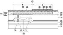
도 4는 본 발명의 일실시예에 따른 양면발광 가능한 발광소자가 채용된 화소회로의 개략적인 부분 측단면도이다.4 is a schematic partial side cross-sectional view of a pixel circuit employing a double-side light emitting device according to an embodiment of the present invention.
도 5는 본 발명의 다른 일실시예에 따른 양면발광 가능한 발광소자가 채용된 화소회로의 개략적인 부분 측단면도이다.5 is a schematic partial side cross-sectional view of a pixel circuit employing a double-sided light emitting device according to another embodiment of the present invention.
도 6은 본 발명의 다른 일실시예에 따른 양면발광 가능한 발광소자가 채용된 화소회로의 개략적인 부분 측단면도이다.6 is a schematic partial side cross-sectional view of a pixel circuit employing a double-sided light emitting device according to another embodiment of the present invention.
♣ 도면의 주요부분에 대한 상세한 설명 ♣ ♣ Detailed description of the main parts of the drawing ♣
310 : 박막트랜지스터320, 420, 520, 620 : 발광소자310:
A : 전면발광부322a,422a,522a,622a : 반사성도전층A: front
322b,422b,522b,622b:제1 하부전극324,424,524,624 : 제1 상부전극322b, 422b, 522b, 622b: first
B : 배면발광부322,422,522,622 : 제2 하부전극B: rear light emitting unit 322,422,522,622: second lower electrode
324,424,524,624 : 제2 상부전극425,625 : 상부보조전극층324,424,524,624: second upper electrode 425,625: upper auxiliary electrode layer
본 발명은 양면발광가능한 발광소자를 포함하는 발광표시장치에 관한 것으로, 보다 구체적으로는, 전면 발광영역 하부에 박막트랜지스터 등을 포함하는 구동회로를 형성함으로써 개구율을 극대화시킨 발광표시장치에 관한 것이다.The present invention relates to a light emitting display device including a light emitting device capable of emitting both sides, and more particularly, to a light emitting display device in which an aperture ratio is maximized by forming a driving circuit including a thin film transistor under the front light emitting area.
일반적으로, 발광표시장치는 외부광원을 필요로 하지 않고, 발광소자가 스스로 발광하여 표시하는 장치로서, 특히, 발광효율, 휘도 및 시야각이 뛰어나며 응답속도가 빠르다.In general, the light emitting display device does not require an external light source, and the light emitting device emits light by itself and displays the light emitting device. In particular, the light emitting display device has excellent light emission efficiency, brightness, viewing angle, and fast response speed.
이하에서는 도면을 참조하여 종래 양면발광 가능한 발광소자를 구체적으로 설명한다.Hereinafter, a conventional double-sided light emitting device will be described in detail with reference to the accompanying drawings.
도 1은 종래의 양면 발광가능한 발광소자의 구조를 나타내는 개략적인 단면도이다.1 is a schematic cross-sectional view showing the structure of a conventional double-sided light emitting device.
도 1을 참조하면, 양면 발광가능한 발광소자(100)는, 기판(110) 상에 형성되는 제1 전극(애노드전극;120)과, 제1 전극(110) 상에 형성되는 발광층(130)과, 발광층(130) 상에 형성되는 제2 전극(캐소드전극;140)을 포함한다.Referring to FIG. 1, a double-sided
일반적으로, 기판(110)은 투명성이 있는 유리 및 플라스틱과 같은 절연기판 등을 이용한다. 제1 전극(120)은 도전성 금속산화물, 예를 들면, ITO(indium tin oxide), IZO(indium zinc oxide) 및 ITZO(indium tin zinc oxide) 등과 같은 투명전극으로 형성된다. 또한, 제2 전극(140)은 일함수가 낮은 금속층, 예컨대, MgAg, Ca 등을 매우 얇게, 바람직하게는, 100Å이내로 증착함으로써 형성되며, 이 제2 전극(124) 상에는 ITO 등과 같은 투명전극이 보조전극(미도시)으로 형성되기도 한다.In general, the
이러한 구조의 발광소자(100) 제1 전극(120)과 제2 전극(140)으로부터의 전자와 정공이 발광층(130)에서 재결합하여 여기자를 형성함으로써 빛을 발생시킨다. 이때, 발광층(130)에는 전자와 정공의 주입특성을 향상시키기 위해 도시하지 않은 정공주입층, 정공수송층, 전자수송층 및 전자주입층 중 적어도 하나의 층들이 더 포함될 수 있다.In the
그러나, 전술한 구조의 종래의 발광소자는 하나의 발광층과 제1 및 제2 전극(애노드전극 및 캐소드전극)을 이용하여 양면발광을 구현하기 때문에, 어느 일측 화면에 표시되는 화상이 타측 화면에 표시될 수 있으며, 서로 다른 화면측으로 타측광이 유입되어 화질을 저하시킬 수 있으며, 주위환경의 조도에 따라 화상표시에 대한 시인성이 떨어질 수도 있다.However, the conventional light emitting device having the above-described structure implements double-sided light emission by using one light emitting layer and first and second electrodes (anode electrode and cathode electrode), so that an image displayed on one screen is displayed on the other screen. The other side light may be introduced to different screens, thereby degrading the image quality, and the visibility of the image display may be deteriorated according to the illuminance of the surrounding environment.
따라서, 본 발명은 전술한 문제점들을 해소하기 위해 제안된 발명으로, 본 발명의 목적은 일측 화상이 타측 화면에 표시되는 것을 방지할 수 있으며, 화상을 명확하게 표시할 수 있을 뿐만 아니라 개구율을 향상시킬 수 있는 발광표시장치를 제공하는 것이다.Accordingly, the present invention has been proposed to solve the above problems, and an object of the present invention is to prevent one image from being displayed on the other screen, to clearly display the image, and to improve the aperture ratio. It is to provide a light emitting display device.
전술한 목적을 달성하기 위한, 본 발명은 기판 상에 형성되는 적어도 하나의 발광소자와, 복수의 데이터선, 복수의 주사선, 복수의 전원선, 적어도 하나의 박막트랜지스터 및 적어도 하나의 캐패시터를 구비하여 상기 발광소자를 발광시키는 구동회로를 포함하는 발광표시장치에 관한 것으로, 상기 발광소자는, 상기 박막트랜지스터의 상부에 형성되며 반사성 도전층을 포함하는 제1 하부전극과, 상기 제1 하부전극 상에 형성되는 제1 발광층과, 상기 발광층 상에 형성되는 제1 상부전극을 구비하는 전면발광부; 및 상기 박막트랜지스터의 상부에 형성되며 투명도전층을 포함하고, 상기 제1 하부전극과 전기적으로 연결된 제2 하부전극과, 상기 제2 하부전극 상에 형성되는 제2 발광층과, 상기 제2 발광층 상에 형성되는 제2 상부전극과, 상기 제2 상부전극 상에 상기 제2 발광층과 대응되게 형성되는 상부보조전극층을 구비하는 배면발광부를 포함한다.In order to achieve the above object, the present invention comprises at least one light emitting element formed on a substrate, a plurality of data lines, a plurality of scanning lines, a plurality of power lines, at least one thin film transistor and at least one capacitor A light emitting display device comprising a driving circuit for emitting light of the light emitting device, wherein the light emitting device includes: a first lower electrode formed on an upper portion of the thin film transistor and including a reflective conductive layer; A front light emitting unit having a first light emitting layer formed thereon and a first upper electrode formed on the light emitting layer; And a second lower electrode formed on the thin film transistor and including a transparent conductive layer, electrically connected to the first lower electrode, a second light emitting layer formed on the second lower electrode, and on the second light emitting layer. And a rear light emitting part including a second upper electrode to be formed and an upper auxiliary electrode layer formed on the second upper electrode to correspond to the second light emitting layer.
바람직하게, 상기 제1 하부전극은 상기 박막트랜지스터와 전기적으로 접촉되는 상기 반사성 도전층 상에 투명성이 있는 하부도전층을 더 포함한다. 상기 상부보조전극층은 알루미늄, 은, 알루미늄합금, 은합금 중 적어도 하나에서 선택된다. 상기 제1 발광층과 상기 제2 발광층이 일체로 형성된다. 상기 제2 하부전극은 상기 제1 하부전극의 상면으로 연장되게 형성된다. 상기 제1 하부전극과 상기 제2 하부전극 간 단차를 줄이기 위해 적어도 상기 제2 하부전극 하부에 형성되는 보조절연층을 더 포함한다.Preferably, the first lower electrode further includes a lower conductive layer having transparency on the reflective conductive layer in electrical contact with the thin film transistor. The upper auxiliary electrode layer is selected from at least one of aluminum, silver, aluminum alloy, silver alloy. The first light emitting layer and the second light emitting layer are integrally formed. The second lower electrode is formed to extend to an upper surface of the first lower electrode. An auxiliary insulating layer is formed on at least a lower portion of the second lower electrode in order to reduce the step difference between the first lower electrode and the second lower electrode.
이하에서는 실시예 도면을 참조하여 본 발명을 구체적으로 설명한다.Hereinafter, the present invention will be described in detail with reference to the accompanying drawings.
도 2는 본 발명에 따른 발광소자를 구현하는 화소회로를 나타내는 회로도이고, 도 3은 본 발명의 일실시예에 따른 양면 발광가능한 발광소자가 채용된 화소회로의 개략적인 부분 측단면도이다.2 is a circuit diagram illustrating a pixel circuit implementing a light emitting device according to the present invention, and FIG. 3 is a schematic partial side cross-sectional view of a pixel circuit employing a double-sided light emitting device according to an embodiment of the present invention.
도 2를 참조하면, 화소회로(300)는 발광소자(320)와, 발광소자(320)로 전류 등의 전원을 전달하는 구동회로(Ⅲ)를 포함한다.Referring to FIG. 2, the pixel circuit 300 includes a
구동회로(Ⅲ)는 제1 트랜지스터(M1), 캐패시터(Cst) 및 제2 트랜지스터(M2)를 포함한다. 또한, 화소회로(300)에는 제1 트랜지스터(M1), 캐패시터(Cst) 및 제2 트랜지스터(M2;310, 도 2 참조) 중 적어도 하나에 연결되는 주사선(Sn), 데이터선(Dm) 및 전원선(Vdd)이 마련되어 있다. 여기서, 주사선(Sn)은 행방향으로 형성되고, 데이터선(Dm) 및 전원선(Vdd)은 열방향으로 형성된다.The driving circuit III includes a first transistor M1, a capacitor Cst and a second transistor M2. In addition, the pixel circuit 300 includes a scan line Sn, a data line Dm, and a power source connected to at least one of the first transistor M1, the capacitor Cst, and the second transistor M2; 310 (see FIG. 2). Line Vdd is provided. Here, the scanning line Sn is formed in the row direction, and the data line Dm and the power supply line Vdd are formed in the column direction.
도 3을 참조하면, 기판(301) 상에는 버퍼층(302), 반도체층(303), 게이트절연막(304), 게이트전극(311), 층간절연막(305), 소스/드레인전극(312) 및 보호막(306)이 형성됨으로써, 구동회로(Ⅲ)를 구성하는 소자들이 제조된다. 그 다음, 게이트전극(311), 소스/드레인전극(312)으로 구성되는 박막트랜지스터(310) 상부에는 박막트랜지스터(310)의 소스/드레인전극(312) 중 적어도 하나와 전기적으로 연결되는 발광소자(OLED ; 320)가 형성된다.Referring to FIG. 3, a
상기 발광소자(320)는 전면발광부(A)와 배면발광부(B)를 포함한다.The
전면발광부(A)는 반사성 도전층(322a)과 하부도전층(322b)를 포함하는 제1 하부전극(제1 애노드전극 ; 322)과, 제1 하부전극(322) 상에 형성되는 제1 발광층(323)과, 제1 발광층(323) 상에 형성되는 제1 상부전극(제1 캐소드전극 : 324)을 구비한다. 배면발광부(B)는 제2 하부전극(제2 애노드전극 : 322)과, 제2 하부전극(322) 상에 형성되는 제2 발광층(323)과, 제2 발광층(323) 상에 형성되는 제2 상부전극(제2 캐소드전극 : 324)을 구비한다.The front emission part A includes a first lower electrode (first anode electrode) 322 including a reflective
또한, 본 발광표시장치에는 반사성 도전층(322a)의 증착두께와 동일한 두께로 적어도 배면발광부(B)의 제2 하부전극(322) 하부에 형성되는 절연막(307)과, 화소정의막(308)이 형성된다. 절연막(307)은 전면발광부(A)와 배면발광부(B)의 단차를 줄여 화소 불량을 막는 역할을 하지만, 절연막(307)을 형성하는 대신 제1 하부전극(322)의 에지슬롭을 완만하게 하여 단차에 따른 화소 불량을 막을 수 있다. 본 절연막(307)은 본 실시예에 한정되지 않으며, 배면발광부(B)의 하부에만 형성할 수도 있다.In addition, the light emitting display device includes an
보다 구체적으로, 반사성 도전층(322a)은 박막트랜지스터(310)의 소스 및 드레인전극(312) 중 어느 하나와 전기적으로 연결되며, 하부 도전층(322b)은 반사성 도전층(322a) 상에 형성된다. 반사성 도전층(322a)은 은(Ag), 알루미늄(Al), 은을 주체로 하는 합금 및 알루미늄을 주체로 하는 합금 등으로 형성된다. 제2 하부전극(322)은 제1 하부전극(322)의 상면과 연장되게, 즉, 제1 하부전극(322)의 하부도전층(322b)과 제2 하부전극(322)을 일체로 형성한다. 이들은 투명성이 있는 도전 성 금속산화물, 예를 들면, ITO(indium tin oxide) 및 IZO(indium zinc oxide) 등으로 형성된다.More specifically, the reflective
본 실시예에서는 제2 하부전극(322)이 단일층으로 형성되어 있으나, 투명도전층을 더 포함하는 다중층으로 형성될 수 있다. 제1 및 제2 상부전극(324) 역시 일체로 형성되며, 투명성이 있는 도전성 금속산화물, 예를 들면, ITO(indium tin oxide) 및 IZO(indium zinc oxide) 등으로 형성된다. 또한, 제1 상부전극(337)은 MgAg, Ca 등을 매우 얇게, 바람직하게는, 100Å이내로 증착하여 형성하기도 한다.In the present exemplary embodiment, the second
또한, 제1 발광층 및 제2 발광층(323), 역시, 일체로 형성되며, 제1 및 제2 하부전극(322)과 제1 및 제2 상부전극(324)으로부터의 전자와 정공이 재결합하여 여기자를 형성하면서 발광하며, 제1 및 제2 발광층(323)에는 전자와 정공의 주입특성을 향상시키기 위해, 미도시된 정공주입층, 정공수송층, 전자수송층 및 전자주입층 중 적어도 일부층들을 더 포함할 수 있다.In addition, the first light emitting layer and the second
도 4는 본 발명의 일실시예에 따른 양면 발광가능한 발광소자가 채용된 화소회로의 개략적인 부분 측단면도이다. 설명의 편의상, 도 3에 개시된 구성요소와 동일한 구성요소에 대한 구체적인 설명은 생략한다.4 is a schematic partial side cross-sectional view of a pixel circuit employing a double-sided light emitting device according to an embodiment of the present invention. For convenience of description, detailed description of the same components as those shown in FIG. 3 will be omitted.
도 4를 참조하면, 기판(301) 상에는 게이트전극(311), 소스/드레인전극(312)으로 구성된 박막트랜지스터(310)가 형성된다. 박막트랜지스터(310) 상부에는 박막트랜지스터(310)의 소스/드레인전극(312) 중 적어도 하나와 전기적으로 연결되는 발광소자(420)가 형성된다.Referring to FIG. 4, a
발광소자(420)는 전면발광부(A)와 배면발광부(B)를 포함한다.The
전면발광부(A)는 반사성 도전층(422a)과 하부도전층(422a)를 포함하는 제1 하부전극(제1 애노드전극;422)과, 제1 하부전극(422) 상에 형성되는 제1 발광층(423)과, 제1 발광층(423) 상에 형성되는 제1 상부전극(제1 캐소드전극 : 424)를 구비한다. 배면발광부(B)는 제2 하부전극(제2 애노드전극 : 422)과, 제2 하부전극(422) 상에 형성되는 제2 발광층(423)과, 제2 발광층(423) 상에 형성되는 제2 상부전극(제2 캐소드전극 : 424)을 구비한다.The front emission part A includes a first lower electrode (first anode electrode) 422 including a reflective
여기서, 제1 하부전극(422)의 반사성 도전층(422a)은 은(Ag), 알루미늄(Al), 은을 주체로 하는 합금 및 알루미늄을 주체로 하는 합금 등으로 형성된다. 하부도전층(422b)과 제2 하부전극(422)은 일체로 형성되며, 이들은 투명성이 있는 도전성 금속산화물, 예를 들면, ITO(indium tin oxide) 및 IZO(indium zinc oxide) 등으로 형성된다. 제1 및 제2 상부전극(424) 역시 일체로 형성되며, 투명성이 있는 도전성 금속산화물, 예를 들면, ITO(indium tin oxide) 및 IZO(indium zinc oxide) 등으로 형성된다. 또한, 제1 상부전극(424)은 MgAg, Ca 등을 매우 얇게, 바람직하게는, 100Å이내로 증착하여 형성하기도 한다. 제1 및 제2 발광층(423)은 일체로 형성된다.The reflective
한편, 제2 상부전극(424) 상에는 적어도 제2 발광층(423)을 덮는 상부보조전극층(425)이 더 형성된다. 상부보조전극층(425)은 반사율이 높은 은, 알루미늄, 은합금, 알루미늄합금 등의 금속을 사용한다. 상부보조전극층(425)은 배면측의 반사율을 높여 빛이 전면으로 새는 것을 막아주는 역할을 하고 또한 제2 상부전극 (424)의 저항을 줄여주는 역할을 수행한다.Meanwhile, an upper
전술한 구조들에 의해, 발광소자(320,420)에 전원이 인가되면, 제1 및 제2 발광층(323,423)이 발광한다. 이때, 전면발광부(A)측 하부에 형성된 반사성 도전층(322a)은 발광층(323,423)에서 발광된 빛이 기판 하부측으로 투과되지 않도록 모아주는 역할을 수행하며, 배면발광부(B)측에 형성된 상부보조전극층(425)은 제1 및 제2 발광층(323,423)에서 발광된 빛이 제2 상부전극(324,424)측으로 투과되지 않도록 모아주는 역할을 수행한다. 게다가, 전면발광부(A) 하부 측에 박막트랜지스터(310,410) 등이 형성되기 때문에, 전면발광부(A) 측에서 발광된 빛이 배면으로 투과되는 것을 효율적으로 차단할 수 있으며, 배면발광부(B) 측에서 발광된 빛을 배면으로 효율적으로 투과시킬 수 있다.By the above-described structures, when power is applied to the
이하에서는 발광소자를 구성하는 구성요소들의 에지 슬롭을 완만하게 하여 단차에 따른 화소불량을 줄일 수 있는 실시예를 도시한 도 5 및 도 6을 참조하여 설명한다.Hereinafter, an exemplary embodiment in which edge defects of components constituting the light emitting device may be smoothed to reduce pixel defects due to steps may be described with reference to FIGS. 5 and 6.
도 5 및 도 6은 본 발명의 다른 일실시예에 따른 양면발광 가능한 발광소자가 채용된 화소회로의 개략적인 부분 측단면도이다. 설명의 중복을 피하기 위해, 도 3 및 도 4에 개시된 구성요소와 동일한 구성요소에 대한 구체적인 설명 및 작동원리는 생략한다.5 and 6 are schematic partial side cross-sectional views of a pixel circuit employing a double-sided light emitting device according to another embodiment of the present invention. In order to avoid duplication of description, detailed descriptions and operating principles of the same components as those shown in FIGS. 3 and 4 will be omitted.
도 5 및 도 6을 참조하면, 기판(501,602) 상에는 버퍼층(502,602), 반도체층 (503,603), 게이트절연막(504,604), 게이트전극(511,611), 층간절연막(505,605), 소스/드레인전극(512,612) 및 보호막(506,606)을 형성함으로써, 구동회로(Ⅲ, 도 2참조)를 구성하는 소자들을 제조한다. 그 다음, 게이트전극(511,611), 소스/드레인전극(512,612)으로 구성되는 박막트랜지스터(510,610) 상부에는 박막트랜지스터(510,610)의 소스/드레인전극(512,612) 중 적어도 하나와 전기적으로 연결되는 발광소자(OLED ; 520,620)가 형성된다.5 and 6, buffer layers 502 and 602, semiconductor layers 503 and 603,
발광소자(520,620)는 전면발광부(A)와 배면발광부(B)를 포함한다.The
전면발광부(A)는 반사성 도전층(522a,622a)과 하부도전층(522b,622b)를 포함하는 제1 하부전극(제1 애노드전극 ; 522,622)과, 제1 하부전극(522,622) 상에 형성되는 제1 발광층(523,623)과, 제1 발광층(523,623) 상에 형성되는 제1 상부전극(제1 캐소드전극 : 524,624)을 구비한다.The front light emitting portion A is disposed on the first lower electrodes (
배면발광부(B)는 제2 하부전극(제2 애노드전극 : 522,622)과, 제2 하부전극(522,622) 상에 형성되는 제2 발광층(523,623)과, 제2 발광층(523,623) 상에 형성되는 제2 상부전극(제2 캐소드전극 : 524,624)을 구비한다. 한편, 도 6의 배면발광부(B)는 제2 상부전극(624)상에 제2 발광층(423)과 대응하도록 형성된 상부보조전극층(625)을 더 포함한다. 상부보조전극층(625)은 반사율이 높은 은, 알루미늄, 은합금, 알루미늄합금 등의 금속을 사용한다. 상부보조전극층(625)은 배면측의 반사율을 높여 빛이 전면으로 새는 것을 막아주는 역할을 하고 또한 제2 상부전극(624)의 저항을 줄여주는 역할을 수행한다.The bottom light emitting unit B is formed on the second lower electrodes (
하부도전층(522b,622b)과 제2 하부전극(522,622)은 일체로 형성되며, 제1 및 제2 상부전극(524,624)과 제1 및 제2 발광층(523,623)은 모두 일체로 형성된다. 제1 및 제2 하부전극(522,622)과 제1 및 제2 상부전극(524,624)으로부터의 전자와 정공이 재결합하여 여기자를 형성하면서 발광한다.The lower
본 실시예들에서는 제1 하부전극의 하부도전층 및 제2 하부전극, 제1 및 제2 발광층, 제1 및 제2 상부전극을 각각 일체로 형성하는 것이 개시되어 있으나, 각 전극 및 발광층을 별도로 형성할 수 있다. 또한, 본 실시예들에서는 발광소자의 하부에 박막트랜지스터만 개시되어 있는 개략적인 화소회로만 개시되어 있으나, 발광소자의 하부에는 전원선, 데이터선, 커패시터 등을 포함하는 다양한 구동소자들이 더 개시될 수 있다.In the present exemplary embodiments, the lower conductive layer and the second lower electrode, the first and second light emitting layers, and the first and second upper electrodes of the first lower electrode are disclosed, but each electrode and the light emitting layer are separately formed. Can be formed. In addition, in the present exemplary embodiment, only a schematic pixel circuit in which only a thin film transistor is disclosed below the light emitting device is disclosed, but various driving devices including a power line, a data line, a capacitor, etc. may be further disclosed below the light emitting device. Can be.
본 발명의 기술사상은 상기 바람직한 실시예에 따라 구체적으로 기술되었으나, 상기한 실시예는 그 설명을 위한 것이며, 그 제한을 위한 것이 아님을 주지해여 한다. 또한, 본 발명의 기술분야에서 당업자는 본 발명의 기술 사상의 범위 내에서 다양한 실시예가 가능함을 이해할 수 있을 것이다.Although the technical spirit of the present invention has been described in detail according to the above-described preferred embodiment, it should be noted that the above-described embodiment is for the purpose of description and not of limitation. In addition, those skilled in the art will understand that various embodiments are possible within the scope of the technical idea of the present invention.
이상, 설명한 바와 같이, 본 발명에 의하면, 사용자가 원하는 화상을 타측화상에 영향받지 않고 정확하게 표시할 수 있을 뿐만 아니라 박막트랜지스터, 전원선 등 각종 소자들을 전면발광부 하부영역에 형성함으로써, 개구율을 극대화시킬 수 있다.As described above, according to the present invention, it is possible to accurately display the image desired by the user without being affected by the other image, and to maximize the aperture ratio by forming various elements such as a thin film transistor and a power line in the lower area of the front light emitting part. You can.
Claims (7)
Translated fromKoreanPriority Applications (1)
| Application Number | Priority Date | Filing Date | Title |
|---|---|---|---|
| KR1020050029185AKR100714010B1 (en) | 2005-04-07 | 2005-04-07 | LED display device |
Applications Claiming Priority (1)
| Application Number | Priority Date | Filing Date | Title |
|---|---|---|---|
| KR1020050029185AKR100714010B1 (en) | 2005-04-07 | 2005-04-07 | LED display device |
Publications (2)
| Publication Number | Publication Date |
|---|---|
| KR20060107151A KR20060107151A (en) | 2006-10-13 |
| KR100714010B1true KR100714010B1 (en) | 2007-05-04 |
Family
ID=37627517
Family Applications (1)
| Application Number | Title | Priority Date | Filing Date |
|---|---|---|---|
| KR1020050029185AExpired - LifetimeKR100714010B1 (en) | 2005-04-07 | 2005-04-07 | LED display device |
Country Status (1)
| Country | Link |
|---|---|
| KR (1) | KR100714010B1 (en) |
Cited By (1)
| Publication number | Priority date | Publication date | Assignee | Title |
|---|---|---|---|---|
| US9245933B2 (en) | 2013-08-30 | 2016-01-26 | Boe Technology Group Co., Ltd. | Electroluminescent (EL) device and display device |
Families Citing this family (4)
| Publication number | Priority date | Publication date | Assignee | Title |
|---|---|---|---|---|
| KR100892369B1 (en)* | 2007-04-02 | 2009-04-10 | 주식회사 나모텍 | Double sided display organic light emitting diode |
| TWI559064B (en) | 2012-10-19 | 2016-11-21 | Japan Display Inc | Display device |
| KR102637790B1 (en)* | 2018-05-31 | 2024-02-19 | 삼성디스플레이 주식회사 | Display device and manufacturing method thereof |
| KR102570021B1 (en)* | 2018-07-31 | 2023-08-22 | 엘지디스플레이 주식회사 | Organic Light Emitting Diode Display Device And Method Of Fabricating The Same |
Citations (4)
| Publication number | Priority date | Publication date | Assignee | Title |
|---|---|---|---|---|
| JP2004220888A (en) | 2003-01-14 | 2004-08-05 | Shoen Kagi Kofun Yugenkoshi | Double-sided display structure of transparent organic light emitting diode and method of manufacturing the same |
| KR20040099150A (en)* | 2003-05-16 | 2004-11-26 | 가부시키가이샤 한도오따이 에네루기 켄큐쇼 | Light-emitting device and electronic device |
| JP2005038608A (en) | 2003-05-16 | 2005-02-10 | Semiconductor Energy Lab Co Ltd | Display device |
| KR20060081507A (en)* | 2005-01-07 | 2006-07-13 | 삼성에스디아이 주식회사 | Light emitting diode and pixel circuit including light emitting diode |
- 2005
- 2005-04-07KRKR1020050029185Apatent/KR100714010B1/ennot_activeExpired - Lifetime
Patent Citations (4)
| Publication number | Priority date | Publication date | Assignee | Title |
|---|---|---|---|---|
| JP2004220888A (en) | 2003-01-14 | 2004-08-05 | Shoen Kagi Kofun Yugenkoshi | Double-sided display structure of transparent organic light emitting diode and method of manufacturing the same |
| KR20040099150A (en)* | 2003-05-16 | 2004-11-26 | 가부시키가이샤 한도오따이 에네루기 켄큐쇼 | Light-emitting device and electronic device |
| JP2005038608A (en) | 2003-05-16 | 2005-02-10 | Semiconductor Energy Lab Co Ltd | Display device |
| KR20060081507A (en)* | 2005-01-07 | 2006-07-13 | 삼성에스디아이 주식회사 | Light emitting diode and pixel circuit including light emitting diode |
Non-Patent Citations (1)
| Title |
|---|
| 1020040099150 |
Cited By (1)
| Publication number | Priority date | Publication date | Assignee | Title |
|---|---|---|---|---|
| US9245933B2 (en) | 2013-08-30 | 2016-01-26 | Boe Technology Group Co., Ltd. | Electroluminescent (EL) device and display device |
Also Published As
| Publication number | Publication date |
|---|---|
| KR20060107151A (en) | 2006-10-13 |
Similar Documents
| Publication | Publication Date | Title |
|---|---|---|
| US10418430B2 (en) | Display device | |
| KR100804859B1 (en) | Display and Array Boards | |
| US6897478B2 (en) | Flat panel display device with anti-reflection layer having concentration gradient | |
| KR101015851B1 (en) | Organic light emitting display | |
| CN1700830B (en) | Organic electroluminescence display device | |
| CN101615624B (en) | Luminescence display panel and method for fabricating the same | |
| US8598782B2 (en) | Organic electroluminescent device and electronic apparatus | |
| CN110061044A (en) | Organic light emitting display panel and display device | |
| JP2005310782A (en) | Display panel using organic light-emitting diodes | |
| JP2002208491A (en) | Self-luminous display | |
| WO2018120108A1 (en) | Top emission type oled display unit, manufacturing method, and display panel | |
| JP2002318553A (en) | Self-luminous display | |
| JPWO2017195560A1 (en) | Display device and electronic device | |
| KR20140064131A (en) | Multi-display device | |
| KR20220053756A (en) | Display device | |
| KR20220072109A (en) | Display device | |
| KR100684835B1 (en) | Flat panel display panel, method of forming flat panel and flat panel display device using same | |
| KR100453633B1 (en) | an active matrix organic electroluminescence display and a manufacturing method of the same | |
| CN114725163A (en) | display device | |
| KR102543973B1 (en) | Organic light emitting diode display device | |
| JP2005128310A (en) | Display device and electronic device | |
| JP4639588B2 (en) | Electro-optical device and method for manufacturing electro-optical device | |
| KR100714010B1 (en) | LED display device | |
| TW202004721A (en) | Display device and array substrate | |
| KR20030035219A (en) | an active matrix organic electroluminescence display and a manufacturing method of the same |
Legal Events
| Date | Code | Title | Description |
|---|---|---|---|
| A201 | Request for examination | ||
| PA0109 | Patent application | St.27 status event code:A-0-1-A10-A12-nap-PA0109 | |
| PA0201 | Request for examination | St.27 status event code:A-1-2-D10-D11-exm-PA0201 | |
| D13-X000 | Search requested | St.27 status event code:A-1-2-D10-D13-srh-X000 | |
| PG1501 | Laying open of application | St.27 status event code:A-1-1-Q10-Q12-nap-PG1501 | |
| D14-X000 | Search report completed | St.27 status event code:A-1-2-D10-D14-srh-X000 | |
| E902 | Notification of reason for refusal | ||
| PE0902 | Notice of grounds for rejection | St.27 status event code:A-1-2-D10-D21-exm-PE0902 | |
| AMND | Amendment | ||
| E13-X000 | Pre-grant limitation requested | St.27 status event code:A-2-3-E10-E13-lim-X000 | |
| P11-X000 | Amendment of application requested | St.27 status event code:A-2-2-P10-P11-nap-X000 | |
| P13-X000 | Application amended | St.27 status event code:A-2-2-P10-P13-nap-X000 | |
| E601 | Decision to refuse application | ||
| PE0601 | Decision on rejection of patent | St.27 status event code:N-2-6-B10-B15-exm-PE0601 | |
| J201 | Request for trial against refusal decision | ||
| PJ0201 | Trial against decision of rejection | St.27 status event code:A-3-3-V10-V11-apl-PJ0201 | |
| AMND | Amendment | ||
| P11-X000 | Amendment of application requested | St.27 status event code:A-2-2-P10-P11-nap-X000 | |
| P13-X000 | Application amended | St.27 status event code:A-2-2-P10-P13-nap-X000 | |
| PB0901 | Examination by re-examination before a trial | St.27 status event code:A-6-3-E10-E12-rex-PB0901 | |
| B701 | Decision to grant | ||
| PB0701 | Decision of registration after re-examination before a trial | St.27 status event code:A-3-4-F10-F13-rex-PB0701 | |
| GRNT | Written decision to grant | ||
| PR0701 | Registration of establishment | St.27 status event code:A-2-4-F10-F11-exm-PR0701 | |
| PR1002 | Payment of registration fee | St.27 status event code:A-2-2-U10-U11-oth-PR1002 Fee payment year number:1 | |
| PG1601 | Publication of registration | St.27 status event code:A-4-4-Q10-Q13-nap-PG1601 | |
| PN2301 | Change of applicant | St.27 status event code:A-5-5-R10-R11-asn-PN2301 | |
| R18-X000 | Changes to party contact information recorded | St.27 status event code:A-5-5-R10-R18-oth-X000 | |
| R18-X000 | Changes to party contact information recorded | St.27 status event code:A-5-5-R10-R18-oth-X000 | |
| PR1001 | Payment of annual fee | St.27 status event code:A-4-4-U10-U11-oth-PR1001 Fee payment year number:4 | |
| R18-X000 | Changes to party contact information recorded | St.27 status event code:A-5-5-R10-R18-oth-X000 | |
| PR1001 | Payment of annual fee | St.27 status event code:A-4-4-U10-U11-oth-PR1001 Fee payment year number:5 | |
| PR1001 | Payment of annual fee | St.27 status event code:A-4-4-U10-U11-oth-PR1001 Fee payment year number:6 | |
| PN2301 | Change of applicant | St.27 status event code:A-5-5-R10-R11-asn-PN2301 | |
| PN2301 | Change of applicant | St.27 status event code:A-5-5-R10-R14-asn-PN2301 | |
| FPAY | Annual fee payment | Payment date:20130329 Year of fee payment:7 | |
| PR1001 | Payment of annual fee | St.27 status event code:A-4-4-U10-U11-oth-PR1001 Fee payment year number:7 | |
| R18-X000 | Changes to party contact information recorded | St.27 status event code:A-5-5-R10-R18-oth-X000 | |
| FPAY | Annual fee payment | Payment date:20140401 Year of fee payment:8 | |
| PR1001 | Payment of annual fee | St.27 status event code:A-4-4-U10-U11-oth-PR1001 Fee payment year number:8 | |
| PR1001 | Payment of annual fee | St.27 status event code:A-4-4-U10-U11-oth-PR1001 Fee payment year number:9 | |
| R18-X000 | Changes to party contact information recorded | St.27 status event code:A-5-5-R10-R18-oth-X000 | |
| FPAY | Annual fee payment | Payment date:20160329 Year of fee payment:10 | |
| PR1001 | Payment of annual fee | St.27 status event code:A-4-4-U10-U11-oth-PR1001 Fee payment year number:10 | |
| P22-X000 | Classification modified | St.27 status event code:A-4-4-P10-P22-nap-X000 | |
| PR1001 | Payment of annual fee | St.27 status event code:A-4-4-U10-U11-oth-PR1001 Fee payment year number:11 | |
| P22-X000 | Classification modified | St.27 status event code:A-4-4-P10-P22-nap-X000 | |
| FPAY | Annual fee payment | Payment date:20180403 Year of fee payment:12 | |
| PR1001 | Payment of annual fee | St.27 status event code:A-4-4-U10-U11-oth-PR1001 Fee payment year number:12 | |
| FPAY | Annual fee payment | Payment date:20190401 Year of fee payment:13 | |
| PR1001 | Payment of annual fee | St.27 status event code:A-4-4-U10-U11-oth-PR1001 Fee payment year number:13 | |
| PR1001 | Payment of annual fee | St.27 status event code:A-4-4-U10-U11-oth-PR1001 Fee payment year number:14 | |
| PR1001 | Payment of annual fee | St.27 status event code:A-4-4-U10-U11-oth-PR1001 Fee payment year number:15 | |
| R18-X000 | Changes to party contact information recorded | St.27 status event code:A-5-5-R10-R18-oth-X000 | |
| PR1001 | Payment of annual fee | St.27 status event code:A-4-4-U10-U11-oth-PR1001 Fee payment year number:16 | |
| PR1001 | Payment of annual fee | St.27 status event code:A-4-4-U10-U11-oth-PR1001 Fee payment year number:17 | |
| PR1001 | Payment of annual fee | St.27 status event code:A-4-4-U10-U11-oth-PR1001 Fee payment year number:18 | |
| P22-X000 | Classification modified | St.27 status event code:A-4-4-P10-P22-nap-X000 | |
| PC1801 | Expiration of term | St.27 status event code:N-4-6-H10-H14-oth-PC1801 Not in force date:20250408 Ip right cessation event data comment text:Termination Category : EXPIRATION_OF_DURATION |