KR100707887B1 - Display device - Google Patents
Display deviceDownload PDFInfo
- Publication number
- KR100707887B1 KR100707887B1KR1020050044449AKR20050044449AKR100707887B1KR 100707887 B1KR100707887 B1KR 100707887B1KR 1020050044449 AKR1020050044449 AKR 1020050044449AKR 20050044449 AKR20050044449 AKR 20050044449AKR 100707887 B1KR100707887 B1KR 100707887B1
- Authority
- KR
- South Korea
- Prior art keywords
- display device
- electrode
- thin film
- film transistor
- film
- Prior art date
- Legal status (The legal status is an assumption and is not a legal conclusion. Google has not performed a legal analysis and makes no representation as to the accuracy of the status listed.)
- Expired - Fee Related
Links
Images


Classifications
- H—ELECTRICITY
- H10—SEMICONDUCTOR DEVICES; ELECTRIC SOLID-STATE DEVICES NOT OTHERWISE PROVIDED FOR
- H10D—INORGANIC ELECTRIC SEMICONDUCTOR DEVICES
- H10D30/00—Field-effect transistors [FET]
- H10D30/60—Insulated-gate field-effect transistors [IGFET]
- H10D30/67—Thin-film transistors [TFT]
- H10D30/6729—Thin-film transistors [TFT] characterised by the electrodes
- H10D30/673—Thin-film transistors [TFT] characterised by the electrodes characterised by the shapes, relative sizes or dispositions of the gate electrodes
- H—ELECTRICITY
- H10—SEMICONDUCTOR DEVICES; ELECTRIC SOLID-STATE DEVICES NOT OTHERWISE PROVIDED FOR
- H10K—ORGANIC ELECTRIC SOLID-STATE DEVICES
- H10K59/00—Integrated devices, or assemblies of multiple devices, comprising at least one organic light-emitting element covered by group H10K50/00
- H10K59/10—OLED displays
- H10K59/12—Active-matrix OLED [AMOLED] displays
- H—ELECTRICITY
- H10—SEMICONDUCTOR DEVICES; ELECTRIC SOLID-STATE DEVICES NOT OTHERWISE PROVIDED FOR
- H10D—INORGANIC ELECTRIC SEMICONDUCTOR DEVICES
- H10D30/00—Field-effect transistors [FET]
- H10D30/60—Insulated-gate field-effect transistors [IGFET]
- H10D30/67—Thin-film transistors [TFT]
- H10D30/6704—Thin-film transistors [TFT] having supplementary regions or layers in the thin films or in the insulated bulk substrates for controlling properties of the device
- H10D30/6713—Thin-film transistors [TFT] having supplementary regions or layers in the thin films or in the insulated bulk substrates for controlling properties of the device characterised by the properties of the source or drain regions, e.g. compositions or sectional shapes
- H10D30/6715—Thin-film transistors [TFT] having supplementary regions or layers in the thin films or in the insulated bulk substrates for controlling properties of the device characterised by the properties of the source or drain regions, e.g. compositions or sectional shapes characterised by the doping profiles, e.g. having lightly-doped source or drain extensions
- H10D30/6719—Thin-film transistors [TFT] having supplementary regions or layers in the thin films or in the insulated bulk substrates for controlling properties of the device characterised by the properties of the source or drain regions, e.g. compositions or sectional shapes characterised by the doping profiles, e.g. having lightly-doped source or drain extensions having significant overlap between the lightly-doped drains and the gate electrodes, e.g. gate-overlapped LDD [GOLDD] TFTs
- H—ELECTRICITY
- H10—SEMICONDUCTOR DEVICES; ELECTRIC SOLID-STATE DEVICES NOT OTHERWISE PROVIDED FOR
- H10D—INORGANIC ELECTRIC SEMICONDUCTOR DEVICES
- H10D30/00—Field-effect transistors [FET]
- H10D30/60—Insulated-gate field-effect transistors [IGFET]
- H10D30/67—Thin-film transistors [TFT]
- H10D30/6729—Thin-film transistors [TFT] characterised by the electrodes
- H10D30/673—Thin-film transistors [TFT] characterised by the electrodes characterised by the shapes, relative sizes or dispositions of the gate electrodes
- H10D30/6733—Multi-gate TFTs
- H—ELECTRICITY
- H10—SEMICONDUCTOR DEVICES; ELECTRIC SOLID-STATE DEVICES NOT OTHERWISE PROVIDED FOR
- H10D—INORGANIC ELECTRIC SEMICONDUCTOR DEVICES
- H10D30/00—Field-effect transistors [FET]
- H10D30/60—Insulated-gate field-effect transistors [IGFET]
- H10D30/67—Thin-film transistors [TFT]
- H10D30/6757—Thin-film transistors [TFT] characterised by the structure of the channel, e.g. transverse or longitudinal shape or doping profile
- H—ELECTRICITY
- H10—SEMICONDUCTOR DEVICES; ELECTRIC SOLID-STATE DEVICES NOT OTHERWISE PROVIDED FOR
- H10D—INORGANIC ELECTRIC SEMICONDUCTOR DEVICES
- H10D86/00—Integrated devices formed in or on insulating or conducting substrates, e.g. formed in silicon-on-insulator [SOI] substrates or on stainless steel or glass substrates
- H10D86/40—Integrated devices formed in or on insulating or conducting substrates, e.g. formed in silicon-on-insulator [SOI] substrates or on stainless steel or glass substrates characterised by multiple TFTs
- H10D86/411—Integrated devices formed in or on insulating or conducting substrates, e.g. formed in silicon-on-insulator [SOI] substrates or on stainless steel or glass substrates characterised by multiple TFTs characterised by materials, geometry or structure of the substrates
- H—ELECTRICITY
- H10—SEMICONDUCTOR DEVICES; ELECTRIC SOLID-STATE DEVICES NOT OTHERWISE PROVIDED FOR
- H10D—INORGANIC ELECTRIC SEMICONDUCTOR DEVICES
- H10D86/00—Integrated devices formed in or on insulating or conducting substrates, e.g. formed in silicon-on-insulator [SOI] substrates or on stainless steel or glass substrates
- H10D86/40—Integrated devices formed in or on insulating or conducting substrates, e.g. formed in silicon-on-insulator [SOI] substrates or on stainless steel or glass substrates characterised by multiple TFTs
- H10D86/481—Integrated devices formed in or on insulating or conducting substrates, e.g. formed in silicon-on-insulator [SOI] substrates or on stainless steel or glass substrates characterised by multiple TFTs integrated with passive devices, e.g. auxiliary capacitors
- H—ELECTRICITY
- H10—SEMICONDUCTOR DEVICES; ELECTRIC SOLID-STATE DEVICES NOT OTHERWISE PROVIDED FOR
- H10D—INORGANIC ELECTRIC SEMICONDUCTOR DEVICES
- H10D86/00—Integrated devices formed in or on insulating or conducting substrates, e.g. formed in silicon-on-insulator [SOI] substrates or on stainless steel or glass substrates
- H10D86/40—Integrated devices formed in or on insulating or conducting substrates, e.g. formed in silicon-on-insulator [SOI] substrates or on stainless steel or glass substrates characterised by multiple TFTs
- H10D86/60—Integrated devices formed in or on insulating or conducting substrates, e.g. formed in silicon-on-insulator [SOI] substrates or on stainless steel or glass substrates characterised by multiple TFTs wherein the TFTs are in active matrices
- H—ELECTRICITY
- H10—SEMICONDUCTOR DEVICES; ELECTRIC SOLID-STATE DEVICES NOT OTHERWISE PROVIDED FOR
- H10H—INORGANIC LIGHT-EMITTING SEMICONDUCTOR DEVICES HAVING POTENTIAL BARRIERS
- H10H20/00—Individual inorganic light-emitting semiconductor devices having potential barriers, e.g. light-emitting diodes [LED]
- H10H20/80—Constructional details
- H10H20/81—Bodies
- H10H20/813—Bodies having a plurality of light-emitting regions, e.g. multi-junction LEDs or light-emitting devices having photoluminescent regions within the bodies
- H—ELECTRICITY
- H10—SEMICONDUCTOR DEVICES; ELECTRIC SOLID-STATE DEVICES NOT OTHERWISE PROVIDED FOR
- H10K—ORGANIC ELECTRIC SOLID-STATE DEVICES
- H10K50/00—Organic light-emitting devices
- H10K50/80—Constructional details
- H10K50/84—Passivation; Containers; Encapsulations
- H10K50/841—Self-supporting sealing arrangements
- H—ELECTRICITY
- H10—SEMICONDUCTOR DEVICES; ELECTRIC SOLID-STATE DEVICES NOT OTHERWISE PROVIDED FOR
- H10K—ORGANIC ELECTRIC SOLID-STATE DEVICES
- H10K50/00—Organic light-emitting devices
- H10K50/80—Constructional details
- H10K50/84—Passivation; Containers; Encapsulations
- H10K50/842—Containers
- H10K50/8426—Peripheral sealing arrangements, e.g. adhesives, sealants
- H—ELECTRICITY
- H10—SEMICONDUCTOR DEVICES; ELECTRIC SOLID-STATE DEVICES NOT OTHERWISE PROVIDED FOR
- H10K—ORGANIC ELECTRIC SOLID-STATE DEVICES
- H10K50/00—Organic light-emitting devices
- H10K50/80—Constructional details
- H10K50/84—Passivation; Containers; Encapsulations
- H10K50/846—Passivation; Containers; Encapsulations comprising getter material or desiccants
- H—ELECTRICITY
- H10—SEMICONDUCTOR DEVICES; ELECTRIC SOLID-STATE DEVICES NOT OTHERWISE PROVIDED FOR
- H10K—ORGANIC ELECTRIC SOLID-STATE DEVICES
- H10K59/00—Integrated devices, or assemblies of multiple devices, comprising at least one organic light-emitting element covered by group H10K50/00
- H10K59/10—OLED displays
- H10K59/12—Active-matrix OLED [AMOLED] displays
- H10K59/121—Active-matrix OLED [AMOLED] displays characterised by the geometry or disposition of pixel elements
- H10K59/1213—Active-matrix OLED [AMOLED] displays characterised by the geometry or disposition of pixel elements the pixel elements being TFTs
- H—ELECTRICITY
- H10—SEMICONDUCTOR DEVICES; ELECTRIC SOLID-STATE DEVICES NOT OTHERWISE PROVIDED FOR
- H10K—ORGANIC ELECTRIC SOLID-STATE DEVICES
- H10K59/00—Integrated devices, or assemblies of multiple devices, comprising at least one organic light-emitting element covered by group H10K50/00
- H10K59/10—OLED displays
- H10K59/12—Active-matrix OLED [AMOLED] displays
- H10K59/127—Active-matrix OLED [AMOLED] displays comprising two substrates, e.g. display comprising OLED array and TFT driving circuitry on different substrates
- H—ELECTRICITY
- H10—SEMICONDUCTOR DEVICES; ELECTRIC SOLID-STATE DEVICES NOT OTHERWISE PROVIDED FOR
- H10K—ORGANIC ELECTRIC SOLID-STATE DEVICES
- H10K59/00—Integrated devices, or assemblies of multiple devices, comprising at least one organic light-emitting element covered by group H10K50/00
- H10K59/80—Constructional details
- H10K59/87—Passivation; Containers; Encapsulations
- H10K59/871—Self-supporting sealing arrangements
- H10K59/8722—Peripheral sealing arrangements, e.g. adhesives, sealants
- H—ELECTRICITY
- H10—SEMICONDUCTOR DEVICES; ELECTRIC SOLID-STATE DEVICES NOT OTHERWISE PROVIDED FOR
- H10K—ORGANIC ELECTRIC SOLID-STATE DEVICES
- H10K59/00—Integrated devices, or assemblies of multiple devices, comprising at least one organic light-emitting element covered by group H10K50/00
- H10K59/80—Constructional details
- H10K59/87—Passivation; Containers; Encapsulations
- H10K59/874—Passivation; Containers; Encapsulations including getter material or desiccant
- H—ELECTRICITY
- H01—ELECTRIC ELEMENTS
- H01L—SEMICONDUCTOR DEVICES NOT COVERED BY CLASS H10
- H01L2924/00—Indexing scheme for arrangements or methods for connecting or disconnecting semiconductor or solid-state bodies as covered by H01L24/00
- H01L2924/0001—Technical content checked by a classifier
- H01L2924/0002—Not covered by any one of groups H01L24/00, H01L24/00 and H01L2224/00
- H—ELECTRICITY
- H10—SEMICONDUCTOR DEVICES; ELECTRIC SOLID-STATE DEVICES NOT OTHERWISE PROVIDED FOR
- H10K—ORGANIC ELECTRIC SOLID-STATE DEVICES
- H10K2102/00—Constructional details relating to the organic devices covered by this subclass
- H10K2102/301—Details of OLEDs
- H10K2102/302—Details of OLEDs of OLED structures
- H10K2102/3023—Direction of light emission
- H10K2102/3026—Top emission
- H—ELECTRICITY
- H10—SEMICONDUCTOR DEVICES; ELECTRIC SOLID-STATE DEVICES NOT OTHERWISE PROVIDED FOR
- H10K—ORGANIC ELECTRIC SOLID-STATE DEVICES
- H10K50/00—Organic light-emitting devices
- H10K50/80—Constructional details
- H10K50/84—Passivation; Containers; Encapsulations
- H—ELECTRICITY
- H10—SEMICONDUCTOR DEVICES; ELECTRIC SOLID-STATE DEVICES NOT OTHERWISE PROVIDED FOR
- H10K—ORGANIC ELECTRIC SOLID-STATE DEVICES
- H10K50/00—Organic light-emitting devices
- H10K50/80—Constructional details
- H10K50/87—Arrangements for heating or cooling
- H—ELECTRICITY
- H10—SEMICONDUCTOR DEVICES; ELECTRIC SOLID-STATE DEVICES NOT OTHERWISE PROVIDED FOR
- H10K—ORGANIC ELECTRIC SOLID-STATE DEVICES
- H10K59/00—Integrated devices, or assemblies of multiple devices, comprising at least one organic light-emitting element covered by group H10K50/00
- H10K59/10—OLED displays
- H10K59/12—Active-matrix OLED [AMOLED] displays
- H10K59/123—Connection of the pixel electrodes to the thin film transistors [TFT]
- H—ELECTRICITY
- H10—SEMICONDUCTOR DEVICES; ELECTRIC SOLID-STATE DEVICES NOT OTHERWISE PROVIDED FOR
- H10K—ORGANIC ELECTRIC SOLID-STATE DEVICES
- H10K59/00—Integrated devices, or assemblies of multiple devices, comprising at least one organic light-emitting element covered by group H10K50/00
- H10K59/30—Devices specially adapted for multicolour light emission
- H10K59/38—Devices specially adapted for multicolour light emission comprising colour filters or colour changing media [CCM]
- H—ELECTRICITY
- H10—SEMICONDUCTOR DEVICES; ELECTRIC SOLID-STATE DEVICES NOT OTHERWISE PROVIDED FOR
- H10K—ORGANIC ELECTRIC SOLID-STATE DEVICES
- H10K59/00—Integrated devices, or assemblies of multiple devices, comprising at least one organic light-emitting element covered by group H10K50/00
- H10K59/80—Constructional details
- H10K59/8794—Arrangements for heating and cooling
Landscapes
- Physics & Mathematics (AREA)
- Engineering & Computer Science (AREA)
- Microelectronics & Electronic Packaging (AREA)
- Optics & Photonics (AREA)
- Geometry (AREA)
- Electroluminescent Light Sources (AREA)
- Devices For Indicating Variable Information By Combining Individual Elements (AREA)
- Thin Film Transistor (AREA)
Abstract
Translated fromKoreanDescription
Translated fromKorean도 1은 본 발명의 EL(전계 발광) 표시장치의 화소부의 단면 구조를 나타내는 도면.1 is a diagram showing a cross-sectional structure of a pixel portion of an EL (electroluminescence) display device of the present invention.
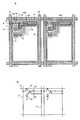
도 2(A) 및 도 2(B)는 EL 표시장치의 화소부의 상면 구조 및 구성을 나타내는 도면.2 (A) and 2 (B) are diagrams showing the top structure and configuration of a pixel portion of an EL display device.
도 3(A)∼도 3(E)는 액티브 매트릭스형 EL 표시장치의 제작공정을 나타내는 도면.3A to 3E are views showing the manufacturing steps of the active matrix EL display device.
도 4(A)∼도 4(D)는 액티브 매트릭스형 EL 표시장치의 제작공정을 나타내는 도면.4A to 4D show manufacturing steps of the active matrix EL display device.
도 5(A)∼도 5(C)는 액티브 매트릭스형 EL 표시장치의 제작공정을 나타내는 도면.5A to 5C show a manufacturing process of an active matrix EL display device.
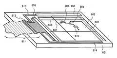
도 6은 EL 모듈의 외관을 나타내는 도면.6 is a view showing an appearance of an EL module;
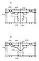
도 7은 EL 표시장치의 회로 블록 구성을 나타내는 도면.7 shows a circuit block configuration of an EL display device;
도 8은 EL 표시장치의 화소부의 확대도.8 is an enlarged view of a pixel portion of an EL display device;
도 9는 EL 표시장치의 샘플링 회로의 소자 구조를 나타내는 도면.9 is a diagram showing an element structure of a sampling circuit of an EL display device;
도 10은 EL 표시장치의 화소부의 구성을 나타내는 도면.10 is a diagram illustrating a configuration of a pixel portion of an EL display device.
도 11은 EL 표시장치의 단면 구조를 나타내는 도면.Fig. 11 shows a cross-sectional structure of an EL display device.
도 12(A) 및 도 12(B)는 EL 표시장치의 화소부의 상면 구조 및 구성을 나타내는 도면.12A and 12B show the top structure and the structure of a pixel portion of an EL display device;
도 13은 EL 표시장치의 화소부의 단면 구조를 나타내는 도면.Fig. 13 is a diagram showing a cross-sectional structure of a pixel portion of an EL display device.
도 14는 EL 표시장치의 화소부의 단면 구조를 나타내는 도면.Fig. 14 shows a cross-sectional structure of a pixel portion of an EL display device.
도 15(A) 및 도 15(B)는 각각 EL 표시장치의 화소부의 상면 구조 및 구성을 나타내는 도면.15A and 15B are diagrams showing the top structure and structure of the pixel portion of the EL display device, respectively.
도 16(A)∼도 16(F)는 전자 장치의 구체 예를 나타내는 도면.16A to 16F are diagrams showing specific examples of the electronic device.
도 17(A) 및 도 17(B)는 EL 모듈의 외관 및 단면을 나타내는 도면.17 (A) and 17 (B) show the appearance and cross section of an EL module.
도 18(A)∼도 18(C)는 콘택트 구조의 제작공정을 나타내는 도면.18 (A) to 18 (C) are diagrams illustrating a fabrication process of a contact structure.
도 19는 EL 층의 적층 구조를 나타내는 도면.19 is a diagram showing a laminated structure of an EL layer.
도 20(A) 및 도 20(B)는 전자 장치의 구체 예를 나타내는 도면.20A and 20B are diagrams showing specific examples of the electronic device.
도 21(A) 및 도 21(B)는 EL 표시장치의 화소부의 구성을 나타내는 도면.21A and 21B show the structure of a pixel portion of an EL display device;
도 22(A) 및 도 22(B)는 EL 표시장치의 화소부의 구성을 나타내는 도면.22A and 22B show the structure of a pixel portion of an EL display device;
도 23은 EL 표시장치의 화소부의 단면 구조를 나타내는 도면.Fig. 23 is a diagram showing a cross-sectional structure of a pixel portion of an EL display device.
<도면의 주요 부분에 대한 부호의 설명><Explanation of symbols for the main parts of the drawings>
11: 기판12: 하지막20: 제1 층간절연막DESCRIPTION OF
41: 제1 패시베이션 막44: 제2 층간절연막41: first passivation film 44: second interlayer insulating film
45: 제2 패시베이션 막46: 화소 전극47: EL 층45
48: 음극49: 보호 전극50: 제3 패시베이션 막48: cathode 49: protective electrode 50: third passivation film
201: 스위칭용 TFT202: 전류제어용 TFT203: EL 소자201: switching TFT 202: current control TFT 203: EL element
본 발명은 기판 상에 제조된 반도체 소자(반도체 박막을 사용한 소자)에 의해 형성된 EL(전계발광) 표시장치로 대표되는 전기광학장치, 및 그 전기광학장치를 디스플레이(표시부로도 칭함)로서 구비한 전자 기기(전자 장치)에 관한 것이다.The present invention provides an electro-optical device represented by an EL (electroluminescence) display device formed by a semiconductor device (a device using a semiconductor thin film) manufactured on a substrate, and the electro-optical device as a display (also referred to as a display). It relates to an electronic device (electronic device).
근년, 기판 상에 TFT(박막트랜지스터)를 형성하는 기술이 대폭으로 진보되고 있고, 액티브 매트릭스형 표시장치에의 응용 개발이 진행되고 있다. 특히, 폴리실리콘 막을 사용한 TFT는 종래의 비정질 규소막을 사용한 TFT보다 더 높은 전계 효과 이동도(이동도로도 칭함)를 가지므로, 고속 동작이 가능하다. 그 때문에, 종래, 기판의 외부에 있는 구동회로에 의해 행해지던 화소 제어를 화소와 동일 기판 상에 형성된 구동회로에 의해 행하는 것이 가능하게 된다.In recent years, the technology for forming a TFT (thin film transistor) on a substrate has been greatly advanced, and the development of application to an active matrix display device is progressing. In particular, a TFT using a polysilicon film has a higher field effect mobility (also referred to as mobility) than a TFT using a conventional amorphous silicon film, so that high speed operation is possible. Therefore, it becomes possible to perform pixel control conventionally performed by a drive circuit external to the substrate by a drive circuit formed on the same substrate as the pixel.
이러한 유형의 액티브 매트릭스형 표시장치는, 동일 기판 상에 각종의 회로 및 소자를 통합시킴으로써 제조 비용의 절감, 표시장치의 소형화, 생산수율의 향상 및 처리량의 증대와 같은 다수의 이점이 얻어질 수 있기 때문에 주목을 받고 있다.In this type of active matrix display device, a number of advantages can be obtained by integrating various circuits and elements on the same substrate, such as reducing manufacturing costs, miniaturizing the display device, improving production yield and increasing throughput. It is getting attention.
액티브 매트릭스형 표시장치에서는, 각 화소를 위한 TFT에 의해 스위칭 소자가 형성되고, 그러한 스위칭 소자를 사용한 드라이버 소자에 의해 전류제어가 행해지고, EL 층(전계발광 층)이 발광하게 된다. 전형적인 화소 구조가, 예를 들어, 미국 특허 제5,684,365호(일본 공개특허공고 평8-234683호)의 도 1에 개시되어 있다.In an active matrix display device, a switching element is formed by TFTs for each pixel, current control is performed by a driver element using such a switching element, and the EL layer (electroluminescent layer) emits light. A typical pixel structure is disclosed, for example, in FIG. 1 of US Pat. No. 5,684,365 (Japanese Patent Application Laid-open No. Hei 8-234683).
상기 미국 특허의 도 1에 도시된 바와 같이, 스위칭 소자(T1)의 드레인이 전류제어 소자(T2)의 게이트 전극에 접속되고, 또한 커패시터(Cs)에도 병렬로 접속되어 있다. 전류제어 소자(T2)의 게이트 전압은 커패시터(Cs)에 축적된 전하에 의해 유지된다.As shown in FIG. 1 of the above-mentioned US patent, the drain of the switching element T1 is connected to the gate electrode of the current control element T2, and also connected in parallel to the capacitor Cs. The gate voltage of the current control element T2 is maintained by the charge accumulated in the capacitor Cs.
반면에, 스위칭 소자(T1)가 비선택 상태에 있을 때, 커패시터(Cs)가 접속되지 않으면 스위칭 소자(T1)를 통해 전하가 누출되고(이 때 흐르는 전류를 오프(off) 전류라 부른다), 전류제어 소자의 게이트 전극에 인가되는 전압이 유지될 수 없게 된다. 이것은 스위칭 소자(T1)가 트랜지스터로 형성되어 있기 때문에 불가피한 문제이다. 그러나, 커패시터(Cs)가 화소 내에 형성되므로, 이것이 화소의 유효 발광 면적(유효 화상 표시 면적)을 감소시키는 요인이 된다.On the other hand, when the switching element T1 is in the unselected state, if the capacitor Cs is not connected, charge leaks through the switching element T1 (the current flowing at this time is called an off current), The voltage applied to the gate electrode of the current control element cannot be maintained. This is an inevitable problem because the switching element T1 is formed of a transistor. However, since the capacitor Cs is formed in the pixel, this becomes a factor of reducing the effective light emitting area (effective image display area) of the pixel.
또한, EL 층을 발광시키기 위해서는, 전류제어 소자(T2)에서 다량의 전류가 흐르는 것이 필요하다. 즉, TFT에 요구되는 성능이 스위칭 소자와 전류제어 소자에서 완전히 다르게 된다. 이러한 경우, 동일 구조의 TFT만으로는 모든 회로 및 소자에 요구되는 성능을 확보하는 것이 곤란하다.In addition, in order to make the EL layer emit light, a large amount of current needs to flow in the current control element T2. In other words, the performance required for the TFT becomes completely different in the switching element and the current control element. In such a case, it is difficult to ensure the performance required for all circuits and elements only with TFTs of the same structure.
본 발명은 상기한 종래 기술을 감안하여 이루어진 것으로, 본 발명의 목적은 동작 성능이 우수하고 신뢰성이 높은 전기광학장치, 특히 EL 표시장치를 제공하는데 있다. 본 발명의 다른 목적은 전기광학장치의 화질을 높임으로써 그 전기광학장치를 디스플레이로서 구비한 전자 기기(전자 장치)의 품질을 향상시키는데 있다.SUMMARY OF THE INVENTION The present invention has been made in view of the above-described prior art, and an object of the present invention is to provide an electro-optical device, particularly an EL display device, having excellent operating performance and high reliability. Another object of the present invention is to improve the quality of an electronic device (electronic device) having the electro-optical device as a display by increasing the image quality of the electro-optical device.
상기 목적들을 달성하기 위해, 본 발명에서는, EL 표시장치의 각 화소에 포함되는 소자들에 요구되는 성능을 감안하여 최적의 구조를 가지는 TFT를 할당한다. 즉, 상이한 구조를 가지는 TFT들이 동일 화소 내에 존재한다. 구체적으로는, 오프 전류값을 충분히 낮추는 것을 가장 중요한 과제로 하는 소자(예를 들어, 스위칭 소자)는 고속 동작보다는 오프 전류값을 감소시키는데 중점을 둔 TFT 구조로 하고, 대전류를 흐르게 하는 것을 가장 중요한 과제로 하는 소자(예를 들어, 전류제어 소자)는 오프 전류값의 감소보다는 대전류 흐름과, 그것과 동시에 현저한 문제가 되는 핫 캐리어 주입으로 인한 열화(劣化)를 억제하는데 중점을 둔 TFT 구조로 한다.In order to achieve the above objects, in the present invention, a TFT having an optimal structure is allocated in view of the performance required for elements included in each pixel of the EL display device. That is, TFTs having different structures exist in the same pixel. Specifically, an element (e.g., a switching element) whose main objective is to sufficiently reduce the off current value is a TFT structure which focuses on reducing the off current value rather than high speed operation, and the most important thing is to flow a large current. A device (for example, a current control device) to be a problem has a TFT structure which focuses on suppressing deterioration due to large current flow and hot carrier injection, which is a significant problem at the same time, rather than a reduction in off current value. .
본 발명에서는, 동일 기판 상에 상기한 바와 같은 적절한 TFT를 나누어 사용함으로써 EL 표시장치의 동작 성능을 높이고 그의 신뢰성을 향상시키는 것이 가능하게 된다. 본 발명의 사상은 화소부에만 한정되는 것이 아니고, 본 발명은 화소부 및 그 화소부를 구동시키는 구동회로부에 포함되는 TFT 구조의 최적화를 도모하는 점에도 특징이 있다.In the present invention, it is possible to improve the operating performance of the EL display device and to improve its reliability by dividing and using the appropriate TFT as described above on the same substrate. The idea of the present invention is not only limited to the pixel portion, but the present invention is also characterized in that the TFT structure included in the pixel portion and the driving circuit portion for driving the pixel portion is optimized.
[실시형태]Embodiment
도 1, 도 2(A) 및 도 2(B)를 사용하여 본 발명의 바람직한 실시형태를 설명한다. 도 1에는 본 발명의 EL 표시장치의 화소의 단면도가 도시되어 있고, 도 2(A)에는 그의 상면도가 도시되어 있고, 도 2(B)에는 그의 회로 구성이 도시되어 있다. 실제로는, 이러한 화소가 매트릭스 형태로 다수 배열되어 화소부(화상 표시부)가 형성된다.1, 2 (A) and 2 (B), a preferred embodiment of the present invention will be described. Fig. 1 is a cross sectional view of a pixel of the EL display device of the present invention, a top view thereof is shown in Fig. 2A, and a circuit configuration thereof is shown in Fig. 2B. In practice, a large number of such pixels are arranged in a matrix to form a pixel portion (image display portion).
도 1의 단면도는 도 2(A)에 도시된 상면도의 A-A'선에 따른 단면을 나타낸 다. 도 1, 도 2(A) 및 도 2(B)에서는 공통의 부호가 사용되고 있으므로, 이들 3개의 도면을 적절히 참조할 수 있다. 또한, 도 2(A)의 상면도에는 2개의 화소가 도시되어 있는데, 모두 동일한 구조이다.1 is a cross-sectional view taken along the line AA ′ of the top view shown in FIG. 2A. Since the common code | symbol is used in FIG.1, FIG.2 (A) and FIG.2 (B), these three figures can be referred suitably. In addition, two pixels are shown in the top view of Fig. 2A, and both have the same structure.
도 1에서, 부호 11은 기판을 나타내고, 부호 12는 하지막을 나타낸다. 기판(11)으로서는, 유리 기판, 유리 세라믹 기판, 석영 기판, 규소 기판, 세라믹 기판, 금속 기판 또는 플라스틱 기판(플라스틱 막을 포함하고 있는)이 사용될 수 있다.In Fig. 1,
또한, 하지막(12)은 가동(可動) 이온을 함유하는 기판 또는 도전성을 가지는 기판이 사용되는 경우에 특히 효과적이지만, 석영 기판에는 형성될 필요가 없다. 하지막(12)으로서는, 규소를 함유한 절연막이 사용될 수 있다. 본 명세서에서 "규소를 함유한 절연막"이란, 구체적으로는 산화규소막, 질화규소막 또는 잘화산화규소막(SiOxNy로 표시됨)과 같은, 규소, 산소 및 질소를 소정 비율로 함유하는 절연막을 가리킨다.Further, the
본 실시형태에서는, 화소 내에 2개의 TFT가 형성되어 있다. 부호 201은 스위칭 소자로서 기능하는 TFT(이후, 스위칭용 TFT라 칭함)를 나타내고, 부호 202는 EL 소자로 흐르는 전류의 양을 제어하는 전류제어 소자로서 기능하는 TFT(이후, 전류제어용 TFT라 칭함)를 나타내며, 양자 모두 n채널형 TFT로 형성되어 있다.In this embodiment, two TFTs are formed in the pixel.
n채널형 TFT의 전계효과 이동도는 p채널형 TFT의 전계효과 이동도보다 더 크므로, 동작 속도가 빠르고 대전류가 용이하게 흐를 수 있다. 또한, 동일 양의 전류 흐름에서도, n채널형 TFT가 보다 더 소형으로 될 수 있다. 따라서, 전류제어용 TFT로서 n채널형 TFT를 사용한 경우에 표시부의 유효 면적이 보다 더 커지므로, 바람직하다.Since the field effect mobility of the n-channel TFT is larger than that of the p-channel TFT, the operation speed is high and a large current can flow easily. Also, even with the same amount of current flow, the n-channel TFT can be made smaller. Therefore, the effective area of the display portion becomes larger when the n-channel TFT is used as the current control TFT, which is preferable.
p채널형 TFT는 핫 캐리어 주입이 거의 문제로 되지 않고 오프 전류값이 낮다는 이점을 가지며, 스위칭용 TFT 및 전류제어용 TFT로서 p채널형 TFT를 사용하는 예들이 이미 보고되어 있다. 그러나, 본 발명에서는, LDD 영역의 위치가 상이한 구조로 함으로써, n채널형 TFT에서도 핫 캐리어 주입 및 오프 전류값의 문제가 해결된다. 본 발명은 모든 화소 내의 모든 TFT를 n채널형 TFT로 하는 점에 특징이 있다.The p-channel TFT has the advantage that the hot carrier injection is hardly a problem and the off current value is low, and examples of using the p-channel TFT as the switching TFT and the current control TFT have already been reported. In the present invention, however, the structure of the LDD region has a different position, thereby solving the problem of hot carrier injection and off current value even in the n-channel TFT. The present invention is characterized in that all TFTs in all pixels are n-channel TFTs.
본 발명에서 스위칭용 TFT 및 전류제어용 TFT를 n채널형 TFT로 한정할 필요는 없고, 스위칭용 TFT 또는 전류제어용 TFT 또는 양자 모두에 p채널형 TFT를 사용하는 것도 가능하다.It is not necessary to limit the switching TFT and the current control TFT to the n-channel TFT in the present invention, and it is also possible to use a p-channel TFT for both the switching TFT or the current control TFT.
스위칭용 TFT(201)는 소스 영역(13), 드레인 영역(14), LDD 영역(15a∼15d), 고농도 불순물 영역(16) 및 채널 형성 영역(17a, 17b)을 포함하는 활성층; 게이트 절연막(18); 게이트 전극(19a, 19b); 제1 층간절연막(20); 소스 배선(21); 및 드레인 배선(22)을 가지도록 형성된다.The switching
도 2(A)에 도시된 바와 같이, 게이트 전극(19a, 19b)이, 상이한 재료(게이트 전극(19a, 19b)보다도 저항이 낮은 재료)로 형성된 게이트 배선(211)에 의해 전기적으로 접속된 이중 게이트 구조로 되어 있는 점이 본 발명의 특징이다. 물론, 이중 게이트 구조뿐만 아니라 삼중 게이트 구조와 같은 소위 멀티게이트 구조(2개 이상의 채널 형성 영역이 직렬 접속된 활성층을 포함하는 구조)도 사용될 수 있다. 멀티게이트 구조는 오프 전류값을 낮추는데 매우 효과적이고, 본 발명에서는 화소의 스위칭용 TFT(201)를 멀티게이트 구조로 함으로써 낮은 오프 전류값의 스위칭 소자를 실현하고 있다.As shown in Fig. 2A, the
활성층은 결정 구조를 포함하는 반도체막으로 형성된다. 즉, 단결정 반도체막이 사용될 수 있고, 다결정 반도체막 또는 미(微)결정 반도체막도 사용될 수 있다는 것이다. 또한, 게이트 절연막(18)은 규소를 함유한 절연막으로 형성될 수 있다. 또한, 게이트 전극, 소스 배선 및 드레인 배선 모두에 도전성 막이 사용될 수 있다.The active layer is formed of a semiconductor film containing a crystal structure. That is, a single crystal semiconductor film can be used, and a polycrystalline semiconductor film or a microcrystalline semiconductor film can also be used. In addition, the
또한, 스위칭용 TFT의 LDD 영역(15a∼15d)은 게이트 절연막(18)을 사이에 두고 게이트 전극(19a, 19b)과 겹치지 않도록 형성된다. 이러한 구조는 오프 전류값을 낮추는데 매우 효과적이다.In addition, the
채널 형성 영역과 LDD 영역 사이에 오프셋 영역(채널 형성 영역과 동일한 조성의 반도체 층을 포함하고 게이트 전압이 인가되지 않는 영역)을 형성하는 것이 오프 전류값을 낮추는데 보다 바람직하다. 또한, 2개 이상의 게이트 전극을 가진 멀티게이트 구조가 사용되는 경우, 채널 형성 영역들 사이에 형성된 고농도 불순물 영역이 오프 전류값을 낮추는데 효과적이다.It is more preferable to form an offset region (a region including a semiconductor layer having the same composition as the channel formation region and to which no gate voltage is applied) between the channel formation region and the LDD region to lower the off current value. In addition, when a multi-gate structure having two or more gate electrodes is used, a high concentration impurity region formed between the channel formation regions is effective to lower the off current value.
상기한 바와 같이, 본 발명에서는 스위칭용 TFT(201)로서 멀티게이트 구조의 TFT를 사용함으로써 오프 전류값이 충분히 낮은 스위칭 소자를 실현하는 것에 특징이 있다. 따라서, 종래의 예에서 설명된 것과 같은 커패시터(Cs)를 형성함이 없이도 충분한 시간(선택되고부터 다음에 선택될 때까지의 기간) 동안 전류제어용 소자 의 게이트 전압을 유지할 수 있다.As described above, the present invention is characterized in that a switching element having a sufficiently low off current value is realized by using a TFT having a multi-gate structure as the switching
즉, 유효 발광 면적의 감소를 야기하는 커패시터를 제거하는 것이 가능하게 되고, 유효 발광 면적을 증대시키는 것이 가능하게 된다. 이것은 EL 표시장치의 화질을 보다 밝게 할 수 있다는 것을 의미한다.That is, it becomes possible to eliminate the capacitor causing the reduction in the effective light emitting area, and to increase the effective light emitting area. This means that the image quality of the EL display device can be made brighter.
다음에, 전류제어용 TFT(202)는 소스 영역(31), 드레인 영역(32), LDD 영역(33) 및 채널 형성 영역(34)을 포함하는 활성층; 게이트 절연막(18); 게이트 전극(35); 제1 층간절연막(20); 소스 배선(36); 및 드레인 배선(37)을 가지도록 형성된다. 게이트 전극(35)은 단일 게이트 구조이지만, 멀티게이트 구조도 사용될 수 있다.Next, the
도 2(A) 및 도 2(B)에 도시된 바와 같이, 스위칭용 TFT(201)의 드레인은 전류제어용 TFT(202)의 게이트에 전기적으로 접속되어 있다. 구체적으로는, 전류제어용 TFT(202)의 게이트 전극(35)이 드레인 배선(접속 배선으로도 불림)(22)을 통해 스위칭용 TFT(201)의 드레인 영역(14)에 전기적으로 접속되어 있다. 또한, 소스 배선(36)은 전류 공급 배선(212)에 접속되어 있다.As shown in Figs. 2A and 2B, the drain of the switching
전류제어용 TFT의 특징은 그의 채널 폭이 스위칭용 TFT(201)의 채널 폭보다 더 크다는 것이다. 즉, 도 8에 도시된 바와 같이, 스위칭용 TFT의 채널 길이를 L1이라 하고, 그의 채널 폭을 W1이라 하고, 전류제어용 TFT의 채널 길이를 L2라 하고, 그의 채널 폭을 W2라고 할 때, W2/L2

멀티게이트 구조의 스위칭용 TFT의 채널 길이(L1)는 형성된 2개 이상의 채널 형성 영역 각각의 채널 길이의 합이다. 도 8의 경우에는 이중 게이트 구조가 형성되어 있으므로, 2개의 채널 형성 영역 각각의 채널 길이(L1a, L1b)의 합이 스위칭용 TFT의 채널 길이(L1)가 된다.The channel length L1 of the switching TFT of the multi-gate structure is the sum of the channel lengths of each of the two or more channel formation regions formed. In the case of Fig. 8, since the double gate structure is formed, the sum of the channel lengths L1a and L1b of each of the two channel formation regions becomes the channel length L1 of the switching TFT.
본 발명에서, 채널 길이(L1, L2) 및 채널 폭(W1, W2)은 특정의 수치 범위 내로 한정되는 것은 아니고, W1은 O.1∼5 ㎛(대표적으로는, 1∼3 ㎛)이고, W2는 0.5∼30 ㎛(대표적으로는, 2∼10 ㎛)인 것이 바람직하다. 이때, L1은 0.2∼18 ㎛(대표적으로는, 2∼15 ㎛)이고, L2는 0.1∼50 ㎛(대표적으로는, 1∼20 ㎛)인 것이 바람직하다.In the present invention, the channel lengths L1 and L2 and the channel widths W1 and W2 are not limited within a specific numerical range, W1 is 0.1 to 5 mu m (typically 1 to 3 mu m), It is preferable that W2 is 0.5-30 micrometers (typically 2-10 micrometers). At this time, it is preferable that L1 is 0.2-18 micrometers (typically 2-15 micrometers), and L2 is 0.1-50 micrometers (typically 1-20 micrometers).
과도한 전류 흐름을 방지하기 위해 전류제어용 TFT의 채널 길이(L2)를 더 길게 설정하는 것이 바람직하다. 바람직하게는, W2/L2

이들 수치 범위 내로 함으로써, VGA급 화소수(640 ×480)를 가진 EL 표시장치로부터 하이비젼급 화소수(1920 ×1080)를 가진 EL 표시장치에 이르는 모든 규격을 망라할 수 있다.By being within these numerical ranges, it is possible to cover all the standards ranging from an EL display device having a VGA class pixel number (640 x 480) to an EL display device having a high vision class pixel number (1920 x 1080).
또한, 스위칭용 TFT에 형성된 LDD 영역의 길이(폭)는 0.5∼3.5 ㎛, 대표적으로는 2.0∼2.5 ㎛로 하는 것이 좋다.In addition, the length (width) of the LDD region formed in the switching TFT is preferably set to 0.5 to 3.5 탆, typically 2.0 to 2.5 탆.
도 1에 도시된 EL 표시장치는 전류제어용 TFT(202)에서 드레인 영역(32)과 채널 형성 영역(34) 사이에 LDD 영역(33)이 형성되는 것을 특징으로 한다. 또한, LDD 영역(33)은 게이트 절연막(18)을 사이에 두고 게이트 전극(35)과 겹치는 영역과, 게이트 전극(35)과 겹치지 않는 영역 모두를 가지고 있다.The EL display device shown in Fig. 1 is characterized in that the
전류제어용 TFT(202)는 EL 소자(203)를 발광시키기 위한 전류를 공급하는 동시에, 그의 공급량을 제어하여 계조 표시를 가능하게 한다. 따라서, 대전류가 흐를 때에도 열화(劣化)가 없고, 핫 캐리어 주입으로 인한 열화에 대한 대책을 강구하는 것이 필요하다. 또한, 검은색을 표시할 때는 전류제어용 TFT(202)를 오프 상태로 하고, 이때 오프 전류값이 높으면 선명한 검은색 표시가 불가능하게 되고, 이것은 콘트라스트 감소와 같은 문제를 초래한다. 따라서, 오프 전류값을 억제하는 것이 필요하다.The
핫 캐리어 주입으로 인한 열화에 관해서는, LDD 영역이 게이트 전극과 겹치는 구조가 매우 효과적인 것으로 알려져 있으나, 전체 LDD 영역이 게이트 전극과 겹치게 되면, 오프 전류값이 증가하므로, 본 발명자는 게이트 전극과 겹치지 않는 LDD 영역이 직렬로 형성되어 있는 신규한 구조에 의해 핫 캐리어 주입과 오프 전류값 모두에 대한 대책을 일시에 해결하였다.As for the deterioration due to hot carrier injection, the structure in which the LDD region overlaps with the gate electrode is known to be very effective. However, when the entire LDD region overlaps with the gate electrode, the off current value increases, so the present inventors do not overlap the gate electrode. Due to the novel structure in which the LDD regions are formed in series, measures for both hot carrier injection and off current values are solved at one time.
이때, 게이트 전극과 겹치는 LDD 영역의 길이는 0.1∼3 ㎛(바람직하게는 0.3∼1.5 ㎛)로 될 수 있다. 그 길이가 너무 길면, 기생 용량이 커지고, 그 길이가 너무 짧으면, 핫 캐리어 방지 효과가 약화된다. 또한, 게이트 전극과 겹치지 않는 LDD 영역의 길이는 1.0∼3.5 ㎛(바람직하게는 1.5∼2.0 ㎛로 설정될 수 있다. 그 길이가 너무 길면, 충분한 전류가 흐를 수 없게 되고, 그 길이가 너무 짧으면, 오프 전류값을 감소시키는 효과가 약화된다.At this time, the length of the LDD region overlapping with the gate electrode may be 0.1 to 3 탆 (preferably 0.3 to 1.5 탆). If the length is too long, the parasitic capacitance becomes large, and if the length is too short, the hot carrier prevention effect is weakened. In addition, the length of the LDD region not overlapping with the gate electrode may be set to 1.0 to 3.5 mu m (preferably 1.5 to 2.0 mu m.) If the length is too long, sufficient current cannot flow and if the length is too short, The effect of reducing the off current value is weakened.
상기한 구조에서 게이트 전극과 LDD 영역이 겹치는 영역에 기생 용량이 형성되므로, 이 영역이 소스 영역(31)과 채널 형성 영역(34) 사이에는 형성되지 않는 것이 바람직하다. 전류제어용 TFT의 경우에는 캐리어(이 경우에는 전자) 흐름 방향이 항상 동일하므로, 드레인 영역 측에만 LDD 영역을 형성해도 충분하다.In the above structure, since the parasitic capacitance is formed in the region where the gate electrode and the LDD region overlap, it is preferable that this region is not formed between the
또한, 흐를 수 있는 전류의 양을 증대시키는 관점에서 보면, 전류제어용 TFT(202)의 활성층(특히, 채널 형성 영역)의 막 두께를 두껍게(바람직하게는 50∼100 ㎛, 더 바람직하게는 60∼80 ㎛) 하는 것도 효과적이다. 역으로, 스위칭용 TFT(201)에서는 오프 전류값을 작게 하는 관점에서 보면, 활성층(특히, 채널 형성 영역)의 막 두께를 얇게(바람직하게는 20∼50 ㎛, 더 바람직하게는 25∼40 ㎛) 하는 것도 효과적이다.Further, from the viewpoint of increasing the amount of current that can flow, the film thickness of the active layer (especially the channel formation region) of the
다음에, 부호 41은 제1 패시베이션 막을 나타내고, 그의 막 두께는 10 ㎚∼1 ㎛(바람직하게는 200∼500 ㎚)로 설정될 수 있다. 이 패시베이션 막의 재료로서는, 규소를 함유한 절연막(특히, 바람직하게는 질화산화규소막 또는 질화규소막)이 사용될 수 있다. 제1 패시베이션 막(41)은 제조된 TFT를 오염물 및 수분으로부터 보호하는 역할을 한다. 최종적으로 TFT 상에 형성되는 EL 층에는 나트륨과 같은 알칼리 금속이 함유된다. 즉, 제1 패시베이션 막(41)은 이들 알칼리 금속(가동 이온)이 TFT 속으로 침입하지 못하도록 하는 보호층으로서 작용한다. 본 명세서 전반에 걸쳐 "알칼리 금속"이라는 용어 내에는 알칼리 금속과 알칼리 토류 금속이 포함된다.Next,
또한, 제1 패시베이션 막(41)이 방열(放熱) 효과를 가지게 함으로써, EL 층 의 열적 열화를 방지하는데에도 효과적이다. 도 1 구조의 EL 표시장치에서는 기판(11) 측으로 광이 방출되므로, 제1 패시베이션 막(41)이 투광성을 가지는 것이 필요하다.In addition, by making the
방열 효과를 가지는 투광성 재료로서는, B(붕소), C(탄소) 및 N(질소)로 이루어진 군에서 선택된 적어도 하나의 원소와, Al(알루미늄), Si(규소) 및 P(인)로 이루어진 군에서 선택된 적어도 하나의 원소를 함유하는 화합물을 들 수 있다. 예를 들어, 질화알루미늄(AlxNy)으로 대표되는 알루미늄 질화물; 탄화규소(SixCy)로 대표되는 규소 탄화물; 질화규소(SixNy)로 대표되는 규소 질화물; 질화붕소(BxNy)로 대표되는 붕소 질화물; 또는 인화붕소(BxPy)로 대표되는 붕소 인화물을 사용할 수 있다. 또한, 산화알루미늄(AlxOy)으로 대표되는 알루미늄 산화물은 투광성이 우수하고, 20 Wm-1K-1의 열전도도를 가지기 때문에, 바람직한 재료 중 하나라고 말할 수 있다. 이들 재료는 방열 효과 뿐만 아니라 수분 및 알칼리 금속과 같은 물질의 침입을 방지하는 효과도 있다. 상기한 투광성 재료에서 x 및 y는 임의의 정수(整數)이다.The light transmissive material having a heat dissipation effect includes at least one element selected from the group consisting of B (boron), C (carbon) and N (nitrogen), and a group consisting of Al (aluminum), Si (silicon), and P (phosphorus). The compound containing the at least 1 element chosen from is mentioned. Aluminum nitrides represented by, for example, aluminum nitride (Alx Ny ); Silicon carbide represented by silicon carbide (Six Cy ); Silicon nitride represented by silicon nitride (Six Ny ); Boron nitride represented by boron nitride (Bx Ny ); Or boron phosphide represented by boron phosphide (Bx Py ). In addition, the aluminum oxide represented by aluminum oxide (Alx Oy ) is excellent in light transmittance and has a thermal conductivity of 20 Wm-1 K-1 , which can be said to be one of preferable materials. These materials have not only a heat dissipation effect but also an effect of preventing the ingress of substances such as moisture and alkali metals. In the above-mentioned translucent material, x and y are arbitrary integers.
상기한 화합물들은 다른 원소와 조합될 수도 있다. 예를 들어, 산화알루미늄에 질소가 첨가된 AlNxOy로 표시되는 질화산화 알루미늄을 사용하는 것도 가능하다. 이 재료도 방열 효과 뿐만 아니라 수분 및 알칼리 금속과 같은 물질의 침입응 방지하는 효과도 있다. 상기한 질화산화 알루미늄에서 x 및 y는 임의의 정수이다.The above compounds may be combined with other elements. For example, it is also possible to use aluminum nitride oxide represented by AlNx Oy in which nitrogen is added to aluminum oxide. This material not only has a heat dissipation effect, but also has an effect of preventing intrusion of substances such as moisture and alkali metals. In the aluminum nitride oxide described above, x and y are arbitrary integers.
또한, 일본 공개특허공고 소62-90260호 공보에 개시된 재료들도 사용될 수 있다. 즉, Si, Al, N, O 및 M을 함유하는 화합물도 사용될 수 있다(M은 희토류 원소, 바람직하게는 Ce(세슘), Yb(이테르븀), Sm(사마륨), Er(에르븀), Y(이트륨), La(란탄), Gd(가돌리늄), Dy(디스프로슘) 및 Nd(네오디뮴)으로 이루어진 군에서 선택된 적어도 하나의 원소이다). 이들 재료도 방열 효과 뿐만 아니라 수분 및 알칼리 금속과 같은 물질의 침입을 방지하는 효과도 있다.In addition, the materials disclosed in Japanese Patent Application Laid-open No. 62-90260 can also be used. That is, compounds containing Si, Al, N, O and M may also be used (M is a rare earth element, preferably Ce (cesium), Yb (ytterbium), Sm (samarium), Er (erbium), Y ( Yttrium), La (lanthanum), Gd (gadolinium), Dy (dysprosium), and Nd (neodymium). These materials also have the effect of preventing the invasion of substances such as moisture and alkali metals as well as the heat radiation effect.
또한, 다이아몬드 박막 또는 비정질 탄소(특히, 다이아몬드의 특성에 가까운 특성을 가지는 것, 다이아몬드와 닮은 탄소(diamond-like carbon)로 불림)와 같은 탄소막도 사용될 수 있다. 이들은 열전도율이 매우 높고, 방열층으로서 매우 효과적이다. 막 두께가 두껍게 되면, 갈색을 띠어 투과율이 감소되므로, 가능한 한 얇은 막 두께(바람직하게는 5∼100 ㎚)를 사용하는 것이 좋다.In addition, carbon films such as diamond thin films or amorphous carbons (particularly those having properties close to those of diamond, called diamond-like carbon) may also be used. They have a very high thermal conductivity and are very effective as a heat dissipation layer. If the film thickness becomes thick, the transmittance decreases because of brown color, and therefore it is preferable to use the film thickness as thin as possible (preferably 5 to 100 nm).
제1 패시베이션 막(41)의 목적은 오염물질 및 수분으로부터 TFT를 보호하는 것이므로, 이 효과를 상실하지 않도록 되어야 한다. 따라서, 상기한 방열 효과를 가지는 재료로 만들어진 박막이 단독으로 사용될 수 있지만, 그러한 박막과, 알칼리 금속 및 수분에 대한 차폐성을 가지는 박막(대표적으로, 질화규소막(SixNy) 또는 질화산화규소막(SiOxNy))을 적층시키는 것이 효과적이다. 상기한 질화규소 및 질화산화규소막에서 x 및 y는 임의의 정수이다.Since the purpose of the
부호 42는 컬러 필터를 나타내고, 부호 43은 형광체(형광 색소 층으로도 불림)을 나타낸다. 양자는 동일한 색의 조합이고, 적색(R), 녹색(G) 또는 청색(B)의 색소를 함유한다. 컬러 필터(42)는 색 순도를 증대시키기 위해 형성되고, 형광제(43)는 색 변환을 행하기 위해 형성된다.
EL 표시장치에는 크게 나누어 다음의 4가지 컬러 표시방식이 있다. 즉, R, G 및 B에 대응하는 3종류의 EL 소자를 형성하는 방식, 백색 발광 EL 소자를 컬러 필터와 조합시키는 방식, 청색 또는 청녹색 발광 EL 소자와 형광체(형광성 색 변환 층(CCM))을 조합시키는 방식, 및 음극(대향 전극)에 투명 전극을 사용하고 R, G 및 B에 대응하는 EL 소자를 중첩시키는 방식이 있다.The EL display device is divided into the following four color display methods. That is, a method of forming three types of EL elements corresponding to R, G, and B, a method of combining a white light emitting EL element with a color filter, and a blue or blue green light emitting EL element and a phosphor (fluorescent color conversion layer (CCM)) There is a method of combining, and a method of using a transparent electrode for the cathode (counter electrode) and superimposing EL elements corresponding to R, G, and B.
도 1의 구조는 청색 발광 EL 소자와 형광체를 조합시키는 방식을 사용하는 경우의 예이다. 여기서는 청색 발광 층이 EL 소자(203)로서 사용되고, 자외광을 포함한 청색 영역 파장을 가지는 광이 형성되고, 형광체(43)는 그 광에 의해 활성화되어 적색, 녹색 또는 청색 광을 방출한다. 컬러 필터(42)에 의해 광의 색 순도가 증대되고, 그러한 광이 출력된다.The structure of FIG. 1 is an example in the case of using the system which combines a blue light emitting EL element and fluorescent substance. Here, a blue light emitting layer is used as the
본 발명은 발광 방식에 관계없이 실시될 수 있고, 상기한 4가지 방식 모두가 본 발명에 사용될 수 있다.The present invention can be implemented irrespective of the light emission method, and all four above-mentioned methods can be used in the present invention.
또한, 컬러 필터(42) 및 형광체(43)를 형성한 후에, 제2 층간절연막(44)에 의해 평탄화를 행한다. 제2 층간절연막(44)으로서는 유기 수지 막이 바람직하고, 폴리이미드, 폴리아미드, 아크릴, BCB(벤조시클로부텐) 중의 하나가 사용될 수 있다. 물론, 충분한 평탄화가 가능하다면 무기 막도 사용할 수 있다.After the
TFT로 인한 단차를 제2 층간절연막(44)으로 평탄화하는 것은 매우 중요하다. 후에 형성되는 EL 층은 매우 얇기 때문에, 단차의 존재로 인해 발광 불량이 일어나 는 경우가 있다. 따라서, 화소 전극을 형성하기 전에 평탄화를 행하여 EL 층을 가능한 한 평탄한 표면에 형성하도록 하는 것이 바람직하다.It is very important to flatten the step caused by the TFT with the second
또한, 제2 층간절연막(44)상에 높은 방열 효과를 가지는 절연막(이후, 방열층이라 칭함)을 형성하는 것이 효과적이다. 5 ㎚∼1 ㎛(대표적으로는 20∼300 ㎚)의 막 두께가 바람직하다. 이러한 방열층은 EL 소자에 의해 발생된 열을 방출하여 EL 소자에 열이 축적되지 않도록 기능한다. 또한, 유기 수지 막으로 형성한 경우에는, 제2 층간절연막(44)이 열에 약하기 때문에, 방열층은 EL 소자에 의해 발생된 열로 인한 악영향을 제2 층간절연막(44)에 부여하지 않도록 작용한다.It is also effective to form an insulating film (hereinafter referred to as a heat dissipating layer) having a high heat dissipation effect on the second
상기한 바와 같이 EL 표시장치의 제조 시에 유기 수지 막에 의해 TFT의 평탄화를 행하는 것이 효과적이지만, EL 소자에 의해 발생된 열로 인한 유기 수지 막의 열화를 고려한 종래의 구조는 존재하지 않는다. 따라서, 방열층을 형성하는 것은 그러한 점을 해결하는데 매우 효과적이라고 말할 수 있다.As described above, it is effective to planarize the TFT by the organic resin film at the time of manufacturing the EL display device, but there is no conventional structure considering the deterioration of the organic resin film due to the heat generated by the EL element. Therefore, it can be said that forming a heat radiation layer is very effective in solving such a point.
또한, 수분, 산소 또는 알칼리 금속에 대하여 불투과성인 재료(제1 패시베이션막(41)의 것과 유사한 재료)가 방열층으로 사용되면, 상기한 바와 같이 열로 인한 EL 소자 및 유기 수지 막의 열화를 방지하는 동시에, EL 층 내의 알칼리 금속이 TFT 쪽으로 확산하지 못하도록 하는 보호층으로도 기능할 수 있다. 또한, 방열층은 수분 및 산소가 TFT로부터 EL 층 내로 침입하지 못하도록 하는 보호층으로도 기능한다.In addition, if a material that is impermeable to moisture, oxygen, or alkali metal (material similar to that of the first passivation film 41) is used as the heat dissipation layer, it is possible to prevent deterioration of the EL element and organic resin film due to heat as described above. At the same time, it can also function as a protective layer which prevents the alkali metal in the EL layer from diffusing to the TFT. The heat dissipation layer also functions as a protective layer that prevents moisture and oxygen from invading the TFT into the EL layer.
특히, 방열 효과가 요구된다면, 다이아몬드 막 또는 다이아몬드와 닮은 탄소(diamond-like carbon) 막과 같은 탄소막이 바람직하고, 수분과 같은 물질의 침입 을 방지하기 위해서는 탄소막과 질화규소막(또는 질화산화규소막)과의 적층 구조를 사용하는 것이 더욱 바람직하다.In particular, if a heat dissipation effect is required, a carbon film such as a diamond film or a diamond-like carbon film is preferable, and a carbon film and a silicon nitride film (or silicon nitride oxide film) may be used to prevent invasion of substances such as moisture. It is more preferable to use the laminated structure with the.
그리하여, 높은 방열 효과를 가지고 수분 및 알칼리 금속을 차단할 수 있는 절연막에 의해 TFT 측과 EL 소자 측이 분리되는 구조가 효과적이다.Thus, the structure in which the TFT side and the EL element side are separated by an insulating film capable of blocking moisture and alkali metal with a high heat radiation effect is effective.
부호 45는 투명 도전 막으로 된 화소 전극(EL 소자의 양극)을 나타낸다. 제2 층간절연막(44) 및 제1 패시베이션 막(41)에 콘택트 홀을 형성한 후, 화소 전극(45)을 전류제어용 TFT(202)의 드레인 배선(37)에 접속되도록 형성한다.
그리고, 화소 전극(45)상에 EL 층(유기 재료가 바람직함)(46), 음극(47) 및 보호 전극(48)을 순서대로 형성한다. EL 층(46)으로서는 단층 구조 또는 적층 구조가 사용될 수 있지만, 적층 구조를 사용하는 경우가 더 많다. 발광층, 전자 수송층, 전자 주입층, 정공 주입층 또는 정공 수송층과 같은 층들의 조합과 같은 각종 적층 구조가 제안되어 있지만, 본 발명에서는 어느 구조라도 사용될 수 있다. EL 층에 형광성 색소를 도핑하는 것도 행해질 수 있다. 본 명세서의 전반에 걸쳐 화소 전극(양극), EL 층 및 음극에 의해 형성된 발광 소자를 EL 소자라 부른다.Then, an EL layer (preferably organic material) 46, a
이미 공지된 모든 EL 재료가 본 발명에 사용될 수 있다. 유기 재료가 그러한 재료로서 널리 알려져 있고, 구동 전압을 고려하면 유기 재료를 사용하는 것이 바람직하다. 예를 들어, 하기의 미국 특허 및 일본 특허출원에 개시된 재료들이 유기 EL 재료로서 사용될 수 있다.All EL materials already known can be used in the present invention. Organic materials are widely known as such materials, and considering the driving voltage, it is preferable to use organic materials. For example, the materials disclosed in the following US patents and Japanese patent applications can be used as the organic EL material.
미국 특허 제4,356,429호, 미국 특허 제4,539,507호, 미국 특허 제4,720,432호, 미국 특허 제4,769,292호, 미국 특허 제4,885,211호, 미국 특허 제4,950,950 호, 미국 특허 제5,059,861호, 미국 특허 제5,047,687호, 미국 특허 제 5,073,446호, 미국 특허 제5,059,862호, 미국 특허 제5,061,617호, 미국 특허 제5,151,629호, 미국 특허 제5,294,869호, 미국 특허 제5,294,870호, 일본 공개특허공고 평10-189525호, 일본 공개특허공고 평8-241048호, 일본 공개특허공고 평8-78159호.U.S. Patent 4,356,429, U.S. Patent 4,539,507, U.S. Patent 4,720,432, U.S. Patent 4,769,292, U.S. Patent 4,885,211, U.S. Patent 4,950,950, U.S. Patent 5,059,861, U.S. Patent 5,047,687, U.S. Patent 5,073,446, U.S. Patent 5,059,862, U.S. Patent 5,061,617, U.S. Patent 5,151,629, U.S. Patent 5,294,869, U.S. Patent 5,294,870, JP 10-189525, JP 8-189525 -241048, Japanese Patent Application Laid-open No. Hei 8-78159.
구체적으로는, 아래의 일반식으로 표시되는 것과 같은 유기 재료가 정공 주입층의 유기 재료로서 사용될 수 있다.Specifically, an organic material such as that represented by the following general formula can be used as the organic material of the hole injection layer.
[화학식 1][Formula 1]

식 1에서, Q는 N 또는 C-R(탄소 체인)이고, M은 금속, 금속 산화물 또는 금속 할로겐화물이고, R은 수소, 알킬, 아르알킬, 아릴 또는 알칼릴이고, T1 및 T2는 수소, 알킬 또는 할로겐과 같은 치환기를 포함하는 불포화 6원 고리이다.In formula 1, Q is N or CR (carbon chain), M is a metal, metal oxide or metal halide, R is hydrogen, alkyl, aralkyl, aryl or alkali, and T1 and T2 are hydrogen, alkyl or Unsaturated 6-membered ring containing a substituent such as halogen.
또한, 아래의 일반식으로 표시되는 테트라아릴디아민을 포함하는 것이 바람직한 방향족 제3 아민이 정공 수송층의 유기 재료로서 사용될 수 있다.In addition, an aromatic tertiary amine, preferably containing tetraaryldiamine represented by the following general formula, may be used as the organic material of the hole transport layer.
[화학식 2][Formula 2]

식 2에서, Are는 아릴렌 기이고, n은 1∼4의 정수이고, Ar, R7, R8, R9는 각각 각종 선택된 아릴 기이다.In Formula 2, Are is an arylene group, n is an integer of 1-4, Ar, R <7> , R <8> , R <9> is each the various selected aryl group.
또한, EL 층, 전자 수송층 또는 전자 주입층의 유기 재료로서는 금속 옥시노이드 화합물이 사용될 수 있다. 아래의 일반식으로 표시되는 것과 같은 재료가 금속 옥시노이드 화합물로서 사용될 수 있다.In addition, a metal oxynoid compound can be used as the organic material of the EL layer, the electron transporting layer, or the electron injection layer. Materials such as those represented by the general formula below may be used as the metal oxynoid compound.
[화학식 3][Formula 3]

R2∼R7은 치환될 수 있고, 다음과 같은 금속 옥시노이드 회힙물도 사용될 수 있다.R2 to R7 may be substituted and the following metal oxynoid aggregates may also be used.
[화학식 4][Formula 4]

식 4에서, R2∼R7은 상기한 바와 같이 정의되고, L1∼L5는 1∼12개의 탄소 원소를 함유하는 탄수화물 기이며, L1과 L2 모두 또는 L2와 L3 모두는 벤조 고리로 형 성된다. 또한, 다음과 같은 금속 옥시노이드 화합물도 사용될 수 있다.In
[화학식 5][Formula 5]

화학식 5에서, R2∼R6은 치환될 수 있다. 그리하여, 유기 리간드(ligand)를 가진 배위 화합물이 유기 EL 재료로서 포함될 수 있다. 상기한 예들은 단지 본 발명의 EL 재료로서 사용될 수 있는 유기 EL 재료의 일부 예에 불과할 뿐이고, EL 재료를 이들에 한정할 필요는 전혀 없다.In
또한, EL 층을 형성하기 위해 잉크 제트법을 사용하는 경우, EL 재료로서 중합체 재료를 사용하는 것이 바람직하다. 대표적인 중합체 재료로서는, 폴리파라페닐렌 비닐렌(PPV) 및 폴리플루오렌과 같은 중합체 재료를 들 수 있다. 컬러화를 위해서는, 예를 들어, 적색 발광재료에 시아노-폴리페닐렌 비닐렌을, 녹색 발광재료에 폴리페닐렌 비닐렌을, 청색 발광재료에 폴리페닐렌 비닐렌 및 폴리알킬페닐렌을 사용하는 것이 바람직하다. 잉크 제트법에 사용될 수 있는 유기 EL 재료와 관해서는, 일본 공개특허공고 평10-012377호 공보에 개시된 모든 재료를 인용할 수 있다.In addition, when the ink jet method is used to form the EL layer, it is preferable to use a polymer material as the EL material. Representative polymer materials include polymer materials such as polyparaphenylene vinylene (PPV) and polyfluorene. For colorization, for example, cyano-polyphenylene vinylene is used as the red light emitting material, polyphenylene vinylene is used as the green light emitting material, and polyphenylene vinylene and polyalkylphenylene is used as the blue light emitting material. It is preferable. As for the organic EL material that can be used for the ink jet method, all materials disclosed in Japanese Patent Application Laid-open No. Hei 10-012377 can be cited.
또한, 음극(47)으로서는, 마그네슘(Mg), 리튬(Li), 세슘(Cs), 바륨(Ba), 칼륨(K), 베릴륨(Be) 또는 칼슘(Ca)과 같은 낮은 일 함수 재료를 함유하는 재료가 사용된다. 바람직하게는, MgAg(Mg:Ag = 10:1의 비율로 Mg와 Ag가 혼합된 재료)로 된 전극이 사용될 수도 있다. 또한, 또 다른 예로서, MgAgAl 전극, LiAl 전극 및 LiFAl 전극을 들 수 있다. 보호 전극(48)은 음극(47)으로의 외부 수분의 침입에 대한 보호막이 되도록 형성되는 전극이고, 알루미늄(Al) 또는 은(Ag)을 함유한 재료가 사용된다. 보호 전극(48)은 방열 효과도 가진다.In addition, the
EL 층(46)과 음극(47)을 대기에의 노출 없이 연속적으로 형성하는 것이 바람직하다. 즉, EL 층 및 음극이 어떠한 유형의 적층 구조를 가지더라도, 멀티체임버(클러스터 공구로도 불림)형의 성막장치에서 모두 연속적으로 형성되는 것이 바람직하다. 이것은, EL 층으로서 유기 재료를 사용할 경우에는 그것이 수분에 매우 약하기 때문에 EL 층이 대기에 노출되었을 때 수분을 흡수하는 것을 피하기 위한 것이다. 또한, EL 층(46)과 음극(47)뿐만 아니라 그 위에 있는 보호 전극(48)까지 연속적으로 형성하는 것이 더욱 바람직하다.It is preferable to form the
EL 층은 열에 매우 약하기 때문에, 성막방법으로서 진공 증착법(특히, 분자 단위 수준의 매우 얇은 막을 형성하는데 유기 분자 빔 증착법이 효과적이다), 스퍼터링법, 플라즈마 CVD법, 스핀 코팅법, 스크린 인쇄법 또는 이온 도금법을 사용하는 것이 바람직하다. 또한, 잉크 제트법에 의해 EL 층을 형성하는 것도 가능하다. 잉크 제트법에는, 공동화(cavitation)를 이용하는 버블 제트법(일본 공개특허공고 평5-116297호 공보 참조)과, 피에조 소자를 이용하는 피에조 방법(일본 공개특허공고 평8-290647호 공보 참조)이 있고, 유기 EL 재료가 열에 약하다는 사실을 고려할 때 피에조 방법이 바람직하다.Since the EL layer is very weak to heat, it is a vacuum deposition method (especially an organic molecular beam deposition method is effective for forming a very thin film on a molecular level) as a film formation method, sputtering method, plasma CVD method, spin coating method, screen printing method or ion. It is preferable to use the plating method. It is also possible to form the EL layer by the ink jet method. The ink jet method includes a bubble jet method using cavitation (see Japanese Laid-Open Patent Publication No. Hei 5-116297) and a piezo method using a piezo element (see Japanese Laid-Open Patent Publication No. Hei 8-290647). In view of the fact that the organic EL material is weak to heat, the piezo method is preferred.
부호 49는 제2 패시베이션 막을 나타내고, 그의 막 두께는 10 ㎚∼1 ㎛(바람직하게는 200∼500 ㎚)로 설정될 수 있다. 제2 패시베이션 막(49)을 형성하는 목적은 주로 EL 층(46)을 수분으로부터 보호하는 것이지만, 제1 패시베이션 막(41)과 마찬가지로 제2 패시베이션 막(49)이 방열 효과를 가지도록 만들어지는 것이 좋다. 따라서, 제2 패시베이션 막(49)의 형성 재료로서는, 제1 패시베이션 막(41)에 사용된 것과 동일한 재료가 사용될 수 있다. EL 층(46)으로서 유기 재료가 사용되는 경우에는 그 층이 산소와의 결합으로 인해 열화되기 때문에, 산소를 쉽게 방출하기 않는 절연막을 사용하는 것이 바람직하다.
또한, 상기한 바와 같이 EL 층이 열에 약하기 때문에, 가능한 한 낮은 온도(바람직하게는 실온으로부터 120℃까지의 온도 범위)에서 성막하는 것이 바람직하다. 따라서, 플라즈마 CVD법, 스퍼터링법, 진공 증착법, 이온 도금법 또는 용액 도포법(스핀 코팅법)이 바람직한 성막방법이라 말할 수 있다.In addition, since the EL layer is weak to heat as described above, it is preferable to form the film at a temperature as low as possible (preferably in a temperature range from room temperature to 120 ° C). Therefore, the plasma CVD method, the sputtering method, the vacuum deposition method, the ion plating method or the solution coating method (spin coating method) can be said to be a preferable film formation method.
본 발명의 EL 표시장치는 상기한 바와 같은 구조의 화소를 포함하는 화소부를 가지고 있고, 그 화소에는 기능에 따라 상이한 구조를 가지는 TFT가 배치되어 있다. 충분히 낮은 오프 전류값을 가지는 스위칭용 TFT와 핫 캐리어 주입에 대하여 강한 전류제어용 TFT가 동일 화소 내에 형성될 수 있고, 그리하여, 신뢰성이 높고 양호한 화상 표시를 할 수 있는 EL 표시장치가 형성될 수 있다.The EL display device of the present invention has a pixel portion including pixels having the above structure, and TFTs having different structures according to functions are disposed in the pixels. A switching TFT having a sufficiently low off current value and a strong current control TFT against hot carrier injection can be formed in the same pixel, and thus an EL display device capable of high reliability and good image display can be formed.
도 1의 화소 구조에서의 가장 중요한 점은 멀티게이트 구조의 TFT가 스위칭용 TFT로서 사용된다는 것이고, LDD 영역의 배치와 같은 것과 관련해서는 도 1의 구조에 한정될 필요는 없다.The most important point in the pixel structure of FIG. 1 is that the TFT of the multi-gate structure is used as the switching TFT, and need not be limited to the structure of FIG. 1 with respect to such arrangement of the LDD region.
이하, 상기한 구조를 가지는 본 발명을 실시예에 의거하여 더욱 상세히 설명한다.Hereinafter, the present invention having the above-described structure will be described in more detail with reference to Examples.
[실시예 1]Example 1
본 실시예를 도 3(A)∼도 5(C)를 사용하여 설명한다. 본 실시예에서는, 화소부와 그 화소부의 주변에 형성된 구동회로부의 TFT를 동시에 제작하는 방법에 관하여 설명한다. 설명을 간단히 하기 위해, 구동회로에 관해서는 기본 회로인 CMOS 회로를 나타내고 있다.This embodiment is demonstrated using FIG. 3 (A)-FIG. 5 (C). In this embodiment, a description will be given of a method of simultaneously manufacturing a pixel portion and TFTs of a driving circuit portion formed around the pixel portion. For simplicity, the driving circuit is a CMOS circuit which is a basic circuit.
먼저, 도 3(A)에 도시된 바와 같이, 유리 기판(300)상에 하지막(301)을 300 ㎚의 두께로 형성한다. 본 실시예에서는 하지막(301)으로서 질화산화규소막을 성막하였다. 이때, 유리 기판(300)과 접촉하는 막의 질소 농도를 10∼25 중량%로 하는 것이 좋다.First, as shown in Fig. 3A, an
또한, 하지막(301)의 일부로서, 도 1에 도시된 제1 패시베이션 막(41)과 동일한 재료로 이루어진 방열층(放熱層)을 형성하는 것이 효과적이다. 전류제어용 TFT에서는 큰 전류가 흘러 열이 쉽게 발생되므로, 전류제어용 TFT에 가능한 한 가깝게 방열층을 형성하는 것이 효과적이다.As a part of the
그 다음, 공지의 성막법에 의해 하지막(301)상에 비정질 규소막(도시되지 않음)을 50 ㎚의 두께로 형성한다. 이것은 비정질 규소막에 한정될 필요는 없고, 비정질 구조를 함유한 반도체막(미(微)결정 반도체막을 포함)이라면 다른 막을 형성할 수도 있다. 또한, 비정질 규소 게르마늄 막과 같은 비정질 구조를 함유한 화합물 반도체막도 사용될 수 있다. 또한, 그의 막 두께는 20∼100 ㎚로 할 수도 있 다.Then, an amorphous silicon film (not shown) is formed on the
그 다음, 공지의 방법으로 비정질 규소막을 결정화하여 결정성 규소막(다결정성 규소막 또는 폴리실리콘 막이라 부르기도 함)(302)을 형성한다. 공지의 결정화 방법으로서는, 전기로(爐)를 사용한 열 결정화법, 레이저를 사용한 레이저 어닐 결정화법 및 적외선 램프를 사용한 램프 어닐 결정화법이 있다. 본 실시예에서는 XeCl 가스를 이용한 엑시머 레이저로부터의 광을 사용하여 결정화를 행하였다.Then, the amorphous silicon film is crystallized by a known method to form a crystalline silicon film (also called a polycrystalline silicon film or a polysilicon film) 302. Known crystallization methods include a thermal crystallization method using an electric furnace, a laser annealing crystallization method using a laser, and a lamp annealing crystallization method using an infrared lamp. In this embodiment, crystallization was performed using light from an excimer laser using XeCl gas.
본 실시예에서는 선 형상으로 가공된 펄스 발진형 엑시머 레이저광을 사용하지만, 직사각형 형상도 사용될 수 있고, 연속 발진형 아르곤 레이저광 및 연속 발진형 엑시머 레이저광도 사용될 수 있다.In this embodiment, a pulse oscillation excimer laser beam processed in a linear shape is used, but a rectangular shape can also be used, and a continuous oscillation argon laser light and a continuous oscillation excimer laser light can also be used.
본 실시예에서는 결정성 규소막을 TFT의 활성층으로 사용하지만, 비정질 규소막을 활성층으로 사용하는 것도 가능하다. 그러나, 전류제어용 TFT는 큰 전류를 흐르게 할 필요성이 있으므로, 전류가 쉽게 흐를 수 있는 결정성 규소막을 사용하는 것이 보다 더 유효하다.In this embodiment, a crystalline silicon film is used as the active layer of the TFT, but it is also possible to use an amorphous silicon film as the active layer. However, since the current control TFT needs to flow a large current, it is more effective to use a crystalline silicon film in which the current can easily flow.
오프 전류를 감소시킬 필요가 있는 스위칭용 TFT의 활성층을 비정질 규소막으로 형성하고, 전류제어용 TFT의 활성층을 결정성 규소막으로 형성하는 것이 효과적이다. 비정질 규소막은 캐리어 이동도가 낮기 때문에 전류가 흐르기 어려워 오프 전류가 쉽게 흐르지 못한다. 즉, 전류가 흐르기 어려운 비정질 규소막과 전류가 흐르기 쉬운 결정성 규소막 모두의 이점이 최대한으로 발휘될 수 있다.It is effective to form the active layer of the switching TFT that needs to reduce the off current into an amorphous silicon film, and to form the active layer of the current control TFT into a crystalline silicon film. Since the amorphous silicon film has a low carrier mobility, current hardly flows, so the off current does not easily flow. That is, the advantages of both the amorphous silicon film in which current does not easily flow and the crystalline silicon film in which current easily flows can be exhibited to the maximum.
그 다음, 도 3(B)에 도시된 바와 같이, 결정성 규소막(302)상에 산화규소막으로 된 보호막(303)을 130 ㎚의 두께로 형성한다. 이 두께는 100∼200 ㎚(바람직 하게는 130∼170 ㎚)의 범위 내에서 선택될 수 있다. 또한, 규소를 함유한 절연막이라면 다른 막을 형성할 수도 있다. 보호막(303)은 불순물의 첨가 시에 결정성 규소막이 플라즈마에 직접 노출되지 않도록 하고 또한 불순물의 섬세한 농도 제어를 가능하게 하기 위해 형성된다.Then, as shown in Fig. 3B, a
그리고, 보호막(303)상에 레지스트 마스크(304a, 304b)를 형성하고, n형 도전성을 부여하는 불순물 원소(이후, n형 불순물 원소라 칭함)를 첨가한다. n형 불순물 원소로서는, 주기율표 15족에 속하는 원소, 전형적으로는 인 또는 비소가 사용될 수 있다. 본 실시예에서는 질량 분리 없이 포스핀(PH3)을 플라즈마 여기하는 플라즈마 도핑법을 사용하고, 인을 1 ×10¹⁸ 원자/㎤의 농도로 첨가하였다. 물론, 질량 분리를 행하는 이온 주입법이 사용될 수도 있다.Then, resist
이 공정에 의해 형성되는 n형 불순물 영역(304, 306)에는 n형 불순물 원소가 2 ×10¹⁶∼5 ×10¹⁹ 원자/㎤(대표적으로는 5 ×10¹⁷∼5 ×10¹⁸ 원자/㎤)의 농도로 함유되도록 도즈량을 조절한다.In the n-
그 다음, 도 3(C)에 도시된 바와 같이, 보호막(303)을 제거하고, 첨가된 주기율표 15족 원소를 활성화시킨다. 활성화 수단으로서는 공지의 활성화 기술을 사용할 수 있으나, 본 실시예에서는 엑시머 레이저광의 조사에 의해 활성화를 행하였다. 펄스 발진형 레이저와 연속 발진형 레이저 모두가 사용될 수 있고, 엑시머 레이저광에 한정될 필요는 없다. 그러나, 첨가된 불순물 원소의 활성화가 목적이므로, 결정성 규소막이 용융되지 않는 정도의 에너지로 레이저광 조사를 행하는 것이 바람직하다. 보호막(303)을 그대로 둔 채 레이저광 조사를 행할 수도 있다.Then, as shown in Fig. 3C, the
레이저광에 의한 불순물 원소의 활성화와 함께 열처리에 의한 활성화를 행할 수도 있다. 열처리에 의해 활성화를 행할 때에는, 기판의 내열성을 고려하여 450∼550℃ 정도로 열처리를 행하는 것이 좋다.In addition to activation of the impurity element by laser light, activation by heat treatment may be performed. When activation is performed by heat treatment, it is preferable to perform heat treatment on the order of 450 to 550 캜 in consideration of the heat resistance of the substrate.
이 공정에 의해, n형 불순물 영역(305, 306)의 엣지(edge), 즉, n형 불순물 영역(305, 306)의 주변에 존재하는 n형 불순물 원소가 첨가되지 않은 영역과의 경계부(접합부)가 명확하게 된다. 이것은 후에 TFT가 완성된 시점에서 LDD 영역과 채널 형성 영역 사이에 매우 양호한 접합부가 형성될 수 있다는 것을 의미한다.By this process, an edge portion of the n-
그 다음, 도 3(D)에 도시된 바와 같이, 결정성 규소막의 불필요한 부분을 제거하여, 섬 형상의 반도체막(이후, 활성층이라 칭함)(307∼310)을 형성한다.Next, as shown in Fig. 3D, unnecessary portions of the crystalline silicon film are removed to form island-like semiconductor films (hereinafter referred to as active layers) 307 to 310. As shown in Figs.
그 다음, 도 3(E)에 도시된 바와 같이, 활성층(307∼310)을 덮도록 게이트 절연막(311)을 형성한다. 게이트 절연막(311)으로서는, 규소를 함유하고 두께가 10∼200 ㎚, 바람직하게는 50∼150 ㎚인 절연막이 사용될 수 있다. 이것은 단층 구조이어도 좋고 또는 적층 구조이어도 좋다. 본 실시예에서는 두께 110 ㎚의 질화산화규소막을 사용하였다.Next, as shown in FIG. 3E, the
그 다음, 두께 200∼400 ㎚의 도전막을 형성하고, 패터닝하여 게이트 전극(312∼316)을 형성한다. 본 실시예에서는, 게이트 전극과 그 게이트 전극에 접속된 인출 배선(이후, 게이트 배선이라 칭힘)을 상이한 재료로 형성하였다. 구체적으로는, 게이트 전극의 것보다 저항이 낮은 재료를 게이트 배선에 사용한다. 그 이유는, 게이트 전극으로서는 미세 가공될 수 있는 재료를 사용하고, 게이트 배선 에는 미세 가공될 수 없을지라도 배선 저항이 낮은 재료를 사용하여야 하기 때문이다. 물론, 게이트 전극과 게이트 배선을 동일한 재료로 형성할 수도 있다.Next, a conductive film having a thickness of 200 to 400 nm is formed and patterned to form
또한, 게이트 배선을 단층의 도전막으로 형성할 수도 있고, 필요한 경우에는 2층 또는 3층의 적층막을 사용하는 것이 바람직할 수도 있다. 게이트 전극의 재료로서는 공지의 모든 도전막을 사용할 수 있다. 그러나, 상기한 바와 같이, 미세 가공될 수 있는 재료, 구체적으로는, 2 ㎛ 이하의 선 폭으로 패터닝될 수 있는 재료를 사용하는 것이 바람직하다.In addition, the gate wiring may be formed by a single layer conductive film, and if necessary, it may be preferable to use a two-layer or three-layer laminated film. As the material of the gate electrode, any known conductive film can be used. However, as mentioned above, it is preferable to use a material that can be microfabricated, specifically, a material that can be patterned with a line width of 2 μm or less.
대표적으로는, 탄탈(Ta), 티탄(Ti), 몰리브덴(Mo), 텅스텐(W) 및 크롬(Cr)으로 이루어진 군에서 선택된 재료의 막, 또는 상기 원소들의 질화물 막(대표적으로, 질화 탄탈 막, 질화 텅스텐 막 또는 질화 티탄 막), 또는 상기 원소들을 조합한 합금막(대표적으로, Mo-W 합금막 또는 Mo-Ta 합금막), 또는 상기 원소들의 규화물 막(대표적으로 규화 텅스텐 막 또는 규화 티탄 막), 또는 도전성을 가지는 규소막이 사용될 수 있다. 물론, 단층 막 또는 적층 막이 사용될 수 있다.Typically, a film of a material selected from the group consisting of tantalum (Ta), titanium (Ti), molybdenum (Mo), tungsten (W) and chromium (Cr), or a nitride film of the elements (typically a tantalum nitride film) , A tungsten nitride film or a titanium nitride film), or an alloy film combining the elements (typically, a Mo-W alloy film or a Mo-Ta alloy film), or a silicide film of the elements (typically a tungsten silicide film or titanium silicide film) Film), or a silicon film having conductivity can be used. Of course, single layer films or laminated films can be used.
본 실시예에서는, 두께 50 ㎚의 질화탄탈(TaN)막과 두께 350 ㎚의 Ta 막으로 된 적층막을 사용하였다. 이 막은 스퍼터링법에 의해 형성하는 것이 좋다. 또한, 스퍼터링 가스로서 Xe 또는 Ne와 같은 불활성 가스를 첨가하면, 응력으로 인한 막의 벗겨짐이 방지될 수 있다.In this embodiment, a laminated film made of a tantalum nitride (TaN) film having a thickness of 50 nm and a Ta film having a thickness of 350 nm was used. This film is preferably formed by sputtering. In addition, when an inert gas such as Xe or Ne is added as the sputtering gas, peeling of the film due to stress can be prevented.
이때, 게이트 전극(313, 316)은 각각 게이트 절연막(311)을 사이에 두고 n형 불순물 영역(305, 306)의 일부와 겹치도록 형성된다. 이 겹침 부분은 후에 게이트 전극과 겹치는 LDD 영역이 된다.In this case, the
그 다음, 도 4(A)에 도시된 바와 같이, 게이트 전극(312∼316)을 마스크로 하여 자기정합적으로 n형 불순물 원소(본 실시예에서는 인)를 첨가한다. 이렇게 하여 형성되는 불순물 영역(317∼323)에는 n형 불순물 영역(305, 306)의 농도의 1/10∼1/2(대표적으로는 1/4∼1/3)의 농도로 인이 첨가되도록 조절한다. 구체적으로는, 1 ×10¹⁶∼5 ×10¹⁸ 원자/㎤(대표적으로는 3 ×10¹⁷∼3 ×10¹⁸ 원자/㎤)의 농도가 바람직하다.Then, as shown in Fig. 4A, n-type impurity elements (phosphorus in this embodiment) are added in self-alignment with the
그 다음, 도 4(B)에 도시된 바와 같이, 게이트 전극들을 덮도록 레지스트 마스크(324a∼324d)를 형성하고, n형 불순물 원소(본 실시예에서는 인)를 첨가하여, 고농도로 인을 함유한 불순물 영역(325∼331)을 형성한다. 여기서도, 포스핀(PH3)을 사용한 이온 도핑법으로 행하고, 이들 영역의 인의 농도가 1 ×10²⁰∼1 ×10²¹ 원자/㎤(대표적으로는 2 ×10²⁰∼5 ×10²⁰ 원자/㎤)로 되도록 이온 도핑을 조절한다.Then, as shown in Fig. 4B, resist
이 공정에 의해 n채널형 TFT의 소스 영역 및 드레인 영역이 형성되고, 스위칭용 TFT에서는 도 4(A)의 공정에서 형성된 n형 불순물 영역(320∼322)의 일부가 잔존한다. 이들 잔존 영역이 도 1의 스위칭용 TFT의 LDD 영역(15a∼15d)에 대응한다.This process forms a source region and a drain region of the n-channel TFT, and a part of the n-
그 다음, 도 4(C)에 도시된 바와 같이, 레지스트 마스크(324a∼324d)를 제거하고, 새로운 레지스트 마스크(332)를 형성한다. 이어서, p형 불순물 원소(본 실시예에서는 붕소)를 첨가하여, 고농도로 붕소를 함유한 불순물 영역(333, 334)을 형성한다. 여기서는, 디보란(B2H6)을 사용한 이온 도핑법에 의해 3 ×10²⁰∼3 ×10²¹ 원자/㎤(대표적으로는 5 ×10²⁰∼1 ×10²¹ 원자/㎤)의 농도로 붕소를 첨가한다.Then, as shown in Fig. 4C, the resist
불순물 영역(333, 334)에는 인이 1 ×10¹⁶∼5 ×10¹⁸ 원자/㎤의 농도로 이미 첨가되어 있지만, 여기서 첨가되는 붕소가 인의 농도의 적어도 3배의 농도로 첨가되기 때문에, 이미 형성되어 있는 n형 불순물 영역이 p형으로 완전히 반전하여 p형 불순물 영역으로서 기능한다.Phosphorus has already been added to the
그 다음, 레지스트 마스크(332)를 제거한 후, 다양한 농도로 첨가된 n형 및 p형 불순물 원소를 활성화시킨다. 활성화 수단으로서는 노 어닐, 레이저 어닐 또는 램프 어닐을 행할 수 있다. 본 실시예에서는, 전기로에서 질소 분위기 중에 550℃로 4시간 열처리를 행하였다.Then, after removing the resist
이때 분위기 중의 산소를 가능한 한 많이 제거하는 것이 중요하다. 이것은 산소가 조금이라도 존재하면 게이트 전극의 노출된 표면이 산화하여 저항의 증가를 초래하는 동시에 후에 옴 접촉(ohmic contact)을 이루기가 더욱 곤란하게 되기 때문이다. 따라서, 상기한 활성화 공정에서의 처리 분위기 중의 산소 농도를 1 ppm 이하, 바람직하게는 0.1 ppm 이하로 하는 것이 바람직하다.At this time, it is important to remove oxygen in the atmosphere as much as possible. This is because if any oxygen is present, the exposed surface of the gate electrode oxidizes, leading to an increase in resistance, and at the same time it becomes more difficult to make an ohmic contact later. Therefore, the oxygen concentration in the processing atmosphere in the above activation step is preferably 1 ppm or less, preferably 0.1 ppm or less.
활성화 공정을 완료한 후에, 두께 300 ㎚의 게이트 배선(335)을 형성한다. 게이트 배선(335)의 재료로서는, 알루미늄(Al) 또는 구리(Cu)를 주성분(조성으로서 50∼100%를 포함)으로 하는 금속막이 사용될 수 있다. 도 2의 게이트 배선(211)과 같이, 스위칭용 TFT의 게이트 전극(314, 315)(도 2의 게이트 전극(19a, 19b)에 대응함)을 전기적으로 접속하도록 하는 배치로 게이트 배선(335)을 형성한다.(도 4(D))After the activation process is completed, a
이러한 구조로 함으로써 게이트 배선의 배선 저항이 극히 작게 될 수 있으므로, 면적이 큰 화상 표시 영역(화소부)을 형성할 수 있다. 즉, 본 실시예의 화소 구조는 화면 크기가 대각선 10인치 이상(또한, 대각선 30인치 이상)인 EL 표시장치를 실현할 수 있기 때문에 매우 효과적이다.With such a structure, the wiring resistance of the gate wiring can be extremely small, so that an image display area (pixel portion) having a large area can be formed. That is, the pixel structure of this embodiment is very effective because the EL display device having a screen size of 10 inches or more diagonally (30 inches or more diagonally) can be realized.
그 다음, 도 5(A)에 도시된 바와 같이, 제1 층간절연막(336)을 형성한다. 제1 층간절연막(336)으로서는 규소를 함유한 절연막을 단층으로 사용하지만, 적층 막을 중간에 조합할 수도 있다. 또한, 400 ㎚∼1.5 ㎛의 막 두께가 사용될 수 있다. 본 실시예에서는, 두께 200 ㎚의 질화산화규소막 상에 두께 800 ㎚의 산화규소막을 적층한 구조가 사용되었다.Next, as shown in Fig. 5A, a first
또한, 3∼100%의 수소를 함유한 분위기에서 300∼400℃로 1∼12시간 열처리하여 수소화 처리를 행한다. 이 공정은 열적으로 활성화된 수소에 의해 반도체막 중의 댕글링 본드(dangling bond)를 수소 종단하는 공정이다. 다른 수소화 수단으로서, 플라즈마 수소화(플라즈마에 의해 활성화된 수소를 사용)를 행할 수도 있다.Further, hydrogenation is performed by heat treatment at 300 to 400 ° C. for 1 to 12 hours in an atmosphere containing 3 to 100% of hydrogen. This step is a step of hydrogen termination of dangling bonds in a semiconductor film by thermally activated hydrogen. As another hydrogenation means, plasma hydrogenation (using hydrogen activated by plasma) can also be performed.
수소화 처리는 제1 층간절연막(336)의 형성 공정 중에 개재될 수도 있다. 즉, 두께 200 ㎚의 질화산화규소막을 형성한 후에 상기한 바와 같이 수소화 처리를 행하고, 이어서 두께 800 ㎚의 산화규소막을 형성할 수도 있다.The hydrogenation process may be interposed during the process of forming the first
그 다음, 제1 층간절연막(336)에 콘택트 홀을 형성하고, 소스 배선(337∼340) 및 드레인 배선(341∼343)을 형성한다. 본 실시예에서는, 이들 배선으로서, 스퍼터링법에 의해 연속적으로 형성된 100 ㎚의 티탄 막, 300 ㎚의 티탄 함유 알루미늄 막 및 150 ㎚의 티탄 막의 3층 구조의 적층막을 사용하였다. 물론, 다른 도전막도 사용될 수 있고, 은, 팔라듐 및 구리를 함유한 합금막도 사용될 수 있다.Next, contact holes are formed in the first
그 다음, 제1 패시베이션 막(344)을 50∼500 ㎚(대표적으로는 200∼300 ㎚)의 두께로 형성한다. 본 실시예에서는 제1 패시베이션 막(344)으로서 두께 300 ㎚의 질화산화규소막을 사용하였다. 이것은 질화규소막으로 대체될 수도 있다. 물론, 도 1의 제1 패시베이션 막(41)과 동일한 재료를 사용하는 것도 가능하다.Next, the
질화산화규소막을 형성하기 전에 H2 또는 NH3과 같은 수소 함유 가스를 사용하여 플라즈마 처리를 행하는 것이 효과적이다. 이 전(前)처리에 의해 활성화된 수소가 제1 층간절연막(336)에 공급되고, 열처리를 행함으로써 제1 패시베이션 막(344)의 막질이 개선된다. 그와 동시에, 제1 층간절연막(336)에 첨가된 수소가 하층 측으로 확산하여, 활성층이 효과적으로 수소화될 수 있다.It is effective to perform a plasma treatment using a hydrogen containing gas such as H2 or NH3 before forming the silicon nitride oxide film. Hydrogen activated by this preprocess is supplied to the first
그 다음, 도 5(B)에 도시된 바와 같이, 컬러 필터(345) 및 형광체(346)를 형성한다. 이들에는 공지의 재료가 사용될 수 있다. 또한, 이들은 별도로 패터닝되어 형성되거나, 또는 연속적으로 형성된 후 함께 패터닝될 수도 있다. 그 성막 방법으로서는, 스크린 인쇄법, 잉크 제트법 또는 마스크 증착법(마스크재를 사용한 선택적 성막 방법) 등의 방법이 사용될 수 있다.Then, as shown in Fig. 5B, the
각각의 막 두께는 0.5∼5 ㎛(대표적으로는 1∼2 ㎛)의 범위 내에서 선택될 수 있다. 특히, 형광체(346)의 최적 막 두께는 사용되는 재료에 따라 다르다. 즉, 막 두께가 너무 얇으면 색변환 효율이 나빠지고, 막 두께가 너무 두꺼우면 단차가 커져서 투과 광량이 떨어진다. 따라서, 최적의 막 두께는 양 특성의 균형을 고려하여 결정되어야 한다.Each film thickness can be selected within the range of 0.5-5 탆 (typically 1-2 탆). In particular, the optimum film thickness of the
본 실시예에서는, EL 층으로부터 발생한 광을 색변환하는 컬러화 방식을 예로 들어 E명하지만, R, G 및 B에 대응하는 EL 층을 개별로 제조하는 방식을 채용하는 경우에는 컬러 필터 및 형광체가 생략될 수 있다.In this embodiment, the colorization method of color conversion of light generated from the EL layer is taken as an example. However, when adopting a method of separately manufacturing the EL layers corresponding to R, G, and B, color filters and phosphors are omitted. Can be.
그 다음, 유기 수지로 제2 층간절연막(347)을 형성한다. 유기 수지로서는, 폴리이미드, 폴리아미드, 아크릴 및 BCB(벤조시클로부텐)와 같은 재료가 사용될 수 있다. 특히, 제2 층간절연막(347)은 평탄화의 의미가 강하므로, 평탄성이 우수한 아크릴이 바람직하다. 본 실시예에서는, 컬러 필터(345)와 형광체(346) 사이의 단차를 충분히 평탄화할 수 있는 막 두께로 아크릴 막을 형성하였다. 이 두께는 1∼5 ㎛(더욱 바람직하게는 2∼4 ㎛)가 바람직하다.Next, a second
그 다음, 제2 층간절연막(347) 및 제1 패시베이션 막(344)에 드레인 배선(343)에 이르는 콘택트 홀을 형성하고, 화소 전극(348)을 형성한다. 본 실시예에서는, 산화인듐-산화주석 화합물(ITO) 막을 110 ㎚의 두께로 형성하고, 패터닝하여 화소 전극을 형성하였다. 화소 전극(348)은 EL 소자의 양극이 된다. 산화인듐-산화아연 화합물 막 또는 산화갈륨을 함유한 산화아연 막과 같은 다른 재료도 사용될 수 있다. 본 실시예에서는, 화소 전극(348)이 드레인 배선(343)을 통해 전류제어용 TFT의 드레인 영역(331)에 전기적으로 접속된 구조로 되어 있다. 이 구조는 다 음과 같은 이점들을 가진다.Next, contact holes reaching the
화소 전극(348)은 EL 층(발광 층) 또는 전하 수송 층과 같은 유기 재료와 직접 접속되어 있기 때문에, EL 층에 함유된 가동(可動) 이온이 화소 전극 전체에 걸쳐 확산하는 것이 가능하다. 즉, 본 실시예의 구조에서는, 화소 전극(348)을 활성층의 일부인 드레인 영역(331)에 직접 접속함이 없이, 개재된 드레인 배선(343)에 의한 활성층에의 가동 이온의 침입이 방지될 수 있다.Since the
그 다음, 도 5(C)에 도시된 바와 같이, EL 층(349), 음극(MgAg 전극)(350) 및 보호 전극(351)을 대기에의 노출 없이 형성한다. 이때, EL 층(349) 및 음극(350)을 형성하기 전에 화소 전극(348)에 열처리를 행하여 수분을 완전히 제거하는 것이 바람직하다. EL 층(349)으로서는 공지의 재료가 사용될 수 있다.Then, as shown in Fig. 5C, an
EL 층(349)으로서는 본 명세서의 실시형태의 부분에서 설명된 재료가 사용될 수 있다. 본 실시예에서는, 도 19에 도시된 바와 같이, 정공 주입층, 정공 수송층, 발광 층 및 전자 수송층의 4층 구조를 가지는 EL 층이 사용되지만, 전자 수송층이 형성되지 않는 경우와 전자 주입층도 형성되는 경우가 있다. 또한, 정공 주입층이 생략되는 경우도 있다. 이들 유형의 조합의 여러 예들이 이미 보고되어 있고, 이들 중 어느 구성이라도 사용될 수 있다.As the
정공 주입층 또는 정공 수송층으로서는 TPD(트리페닐아민 유전체)와 같은 아민이 사용될 수 있고, 또한 히드라존(대표적으로는 DEH), 스틸벤(대표적으로는 STB), 스타버스트(대표적으로는 m-MTDATA)가 사용될 수도 있다. 특히, 유리 전이 온도가 높고 결정화가 어려운 스타버스트 재료가 바람직하다. 또한, 폴리아닐린 (PAni), 폴리티오펜(PEDOT) 및 구리 프탈로시아닌(CuPc)도 사용될 수 있다.As the hole injection layer or the hole transport layer, an amine such as TPD (triphenylamine dielectric) can be used, and also hydrazone (typically DEH), stilbene (typically STB), starburst (typically m-MTDATA) ) May be used. In particular, a starburst material having a high glass transition temperature and being difficult to crystallize is preferable. Polyaniline (PAni), polythiophene (PEDOT) and copper phthalocyanine (CuPc) may also be used.
발광 층 중의 적색 발광 층으로서는 BPPC, 페릴렌 및 DCM이 사용될 수 있고, 특히, Eu(DBM)3(Phen)으로 나타내어지는 Eu 착체(錯體)(상세한 것은Kido, J., et al., Appl. Phys., vol. 35, pp. L394-6, 1996을 참조할 것)가 620 ㎚의 파장에 섬세한 발광을 가지고 단색성이 높다.BPPC, perylene and DCM can be used as the red light emitting layer in the light emitting layer, and in particular, an Eu complex represented by Eu (DBM)3 (Phen) (seeKido, J., et al., Appl. (See Phys., Vol. 35, pp. L394-6, 1996 ) has a monochromatic emission with delicate emission at a wavelength of 620 nm.
또한, 녹색 발광 층으로서는, 대표적으로 퀴나크리돈(quinacridone) 또는 코우마린(coumarin)이 수 몰%의 수준으로 첨가된 Alq3(8-하이드록시퀴놀린 알루미늄)이 사용될 수 있다. 그의 화학식은 다음과 같이 표시된다.In addition, as the green light emitting layer, Alq3 (8-hydroxyquinoline aluminum) in which quinacridone or coumarin is added at a level of several mol% may be used. The chemical formula is represented as follows.
[화학식 6][Formula 6]

또한, 청색 발광 층으로서는, 아미노 치환 DSA가 DSA(디스틸 아릴렌 유도체)에 첨가된 디스틸 아릴렌 아미노 유도체가 사용될 수 있다. 특히, 고성능 재료인 디스틸 비페닐(DPVBi)을 사용하는 것이 바람직하다. 그의 화학식은 다음과 같이 표시된다.In addition, as the blue light emitting layer, a dimethyl arylene amino derivative in which an amino substituted DSA is added to DSA (distyl arylene derivative) can be used. In particular, it is preferable to use the high performance material dityl biphenyl (DPVBi). The chemical formula is represented as follows.
[화학식 7][Formula 7]

또한, 제2 패시베이션 막(352)으로서 두께 300 ㎚의 질화규소막을 형성하는데, 이 막은 보호 전극(351)을 형성한 후에 대기에의 노출 없이 연속적으로 형성될 수 있다. 제2 패시베이션 막(352)의 재료로서는, 물론, 도 1의 제2 패시베이션 막(49)의 것과 동일한 재료가 사용될 수도 있다.Also, as the
본 실시예에서는, 정공 주입층, 정공 수송층, 발광 층 및 전자 주입층으로 이루어진 4층 구조가 사용되지만, 많은 조합의 예들이 이미 보고되어 있고, 이들 중 어느 구성이라도 사용될 수 있다. 또한, 본 실시예에서는, EL 소자의 음극으로서 MgAg 전극을 사용하지만, 다른 공지의 재료가 사용될 수도 있다.In this embodiment, a four-layer structure consisting of a hole injection layer, a hole transport layer, a light emitting layer, and an electron injection layer is used, but many combination examples have already been reported, and any of these configurations can be used. Further, in this embodiment, although the MgAg electrode is used as the cathode of the EL element, other known materials may be used.
또한, 보호 전극(351)은 MgAg 전극(350)의 열화를 방지하기 위해 형성되고, 알루미늄을 주성분으로 하는 금속막이 대표적이다. 물론, 다른 재료도 사용될 수 있다. 또한, EL 층(349) 및 MgAg 전극(350)은 수분에 매우 약하기 때문에, 보호 전극(351)에 이르기까지 대기에의 노출 없이 연속적으로 형성하여 EL 층을 외부 공기로부터 보호하도록 하는 것이 바람직하다.In addition, the
EL 층(349)의 막 두께는 10∼400 ㎚(대표적으로는 60∼160 ㎚)로 할 수 있고, MgAg 전극(350)의 두께는 180∼300 ㎚(대표적으로는 200∼250 ㎚)로 할 수 있 다.The film thickness of the
이렇게 하여, 도 5(C)에 도시된 바와 같은 구조를 가지는 액티브 매트릭스형 EL 표시장치가 완성된다. 본 실시예의 액티브 매트릭스형 EL 표시장치는, 화소부 뿐만 아니라 구동회로부에도 최적의 구조를 가진 TFT를 배치함으로써, 매우 높은 신뢰성을 나타내고, 동작 특성도 향상될 수 있다.In this way, an active matrix EL display device having a structure as shown in Fig. 5C is completed. In the active matrix type EL display device of this embodiment, by disposing a TFT having an optimal structure not only in the pixel portion but also in the driving circuit portion, very high reliability can be obtained and the operation characteristics can be improved.
먼저, 동작 속도의 저하 없이 핫 캐리어 주입을 최대한으로 감소시키는 구조를 가지는 TFT가 구동회로를 형성하는 CMOS 회로의 n채널형 TFT로서 사용된다. 여기서 말하는 구동회로는 시프트 레지스터, 버퍼, 레벨 시프터, 샘플링 회로(전달 게이트라고도 불림)를 포함한다. 디지털 구동이 행해지는 경우에는, D/A 컨버터와 같은 신호 변환 회로도 포함된다.First, a TFT having a structure that reduces hot carrier injection to the maximum without lowering the operation speed is used as an n-channel TFT of a CMOS circuit which forms a driving circuit. The driving circuit here includes a shift register, a buffer, a level shifter, and a sampling circuit (also called a transfer gate). When digital driving is performed, a signal conversion circuit such as a D / A converter is also included.
본 실시예의 경우에는, 도 5(C)에 도시된 바와 같이, n채널형 TFT(205)의 활성층이 소스 영역(355), 드레인 영역(356), LDD 영역(357) 및 채널 형성 영역(358)을 포함하고, LDD 영역(357)이 게이트 절연막(311)을 사이에 두고 게이트 전극(313)과 겹쳐 있다.In the case of this embodiment, as shown in Fig. 5C, the active layer of the n-channel TFT 205 has a
드레인 영역 측에만 LDD 영역을 형성하는 것은 동작 속도를 저하시키지 않는 것을 고려한 것이다. 또한, 이 n채널형 TFT(205)에서는 오프 전류값에 관심을 기울일 필요는 없고, 오히려 동작 속도를 중시하는 것이 좋다. 따라서, LDD 영역(357)이 게이트 전극과 전체적으로 겹쳐 저항 성분을 최대한 감소시키는 것이 바람직하다. 즉, 모든 오프셋을 제거하는 것이 좋다.Forming the LDD region only on the drain region side takes into account that the operation speed is not lowered. In addition, in this n-channel TFT 205, it is not necessary to pay attention to the off current value, but it is better to focus on the operation speed. Therefore, it is preferable that the
핫 캐리어 주입에 의한 CMOS 회로의 p채널형 TFT(206)의 열화가 거의 무시되 기 때문에, LDD 영역이 형성되지 않는다. 물론, n채널형 TFT(205)와 마찬가지로 LDD 영역을 형성하여 핫 캐리어 대책을 강구할 수도 있다.Since the deterioration of the p-channel TFT 206 of the CMOS circuit due to hot carrier injection is almost ignored, no LDD region is formed. Of course, similarly to the n-channel TFT 205, an LDD region may be formed to take hot carrier countermeasures.
구동회로 중에서도 샘플링 회로는 다른 회로와 비교할 때에 다소 특별한 것이고, 채널 형성 영역에서 양 방향으로 큰 전류가 흐른다. 즉, 소스 영역과 드레인 영역의 역할이 바뀐다. 또한, 오프 전류값을 최대한으로 억제하는 것이 필요하고, 그러한 의미에서 스위칭용 TFT와 전류제어용 TFT 사이의 중간 정도의 기능을 가지는 TFT를 배치하는 것이 바람직하다.Among the driving circuits, the sampling circuit is rather special compared with other circuits, and a large current flows in both directions in the channel formation region. In other words, the roles of the source region and the drain region are reversed. In addition, it is necessary to suppress the off current value to the maximum, and in such a sense, it is preferable to arrange a TFT having a function approximately intermediate between the switching TFT and the current control TFT.
따라서, 샘플링 회로를 형성하는 n채널형 TFT로서, 도 9에 도시된 구조를 가지는 TFT를 배치하는 것이 바람직하다. 도 9에 도시된 바와 같이, LDD 영역(901a, 901b)의 일부가 게이트 절연막(902)을 사이에 두고 게이트 전극(903)과 겹쳐 있다. 이것의 효과는 전류제어용 TFT(202)의 설명에서 설명된 바와 같고, 샘플링 회로의 경우는 채널 형성 영역(904)을 사이에 끼우는 형상으로 LDD 영역(901a, 901b)을 형성하는 점이 상이하다.Therefore, it is preferable to arrange the TFT having the structure shown in Fig. 9 as the n-channel TFT forming the sampling circuit. As shown in FIG. 9, portions of the
또한, 도 1에 도시된 구조를 가지는 화소가 형성되어 화소부를 형성한다. 화소 내에 형성되는 스위칭용 TFT 및 전류제어용 TFT의 구조는 도 1에서 이미 설명되었기 때문에, 여기서는 그의 설명을 생략한다.In addition, a pixel having the structure shown in FIG. 1 is formed to form a pixel portion. Since the structures of the switching TFT and the current control TFT formed in the pixel have already been described in FIG. 1, the description thereof is omitted here.
실제로는, 도 5(C)까지의 공정을 완료한 후에, 외부 공기에 노출되지 않도록 기밀성이 높은 보호 막(층상 막 또는 자외선 경화 수지 막 등) 또는 세라믹 밀봉 캔과 같은 하우징 부재를 사용하여 패키징(봉입)을 추가적으로 행하는 것이 바람직하다. 그 경우, 하우징 부재의 내부를 불활성 분위기로 하고 하우징 부재 내에 흡 습성 재료(예를 들어, 산화바륨)를 배치하면, EL 층의 신뢰성(수명)이 증가된다.In fact, after the process up to FIG. 5C is completed, packaging is performed using a housing member such as a high-tightness protective film (such as a layered film or an ultraviolet curable resin film) or a ceramic sealing can so as not to be exposed to external air. Encapsulation) is preferably performed. In that case, if the inside of the housing member is made into an inert atmosphere and a hygroscopic material (for example barium oxide) is placed in the housing member, the reliability (life) of the EL layer is increased.
또한, 패키징 등의 처리에 의해 기밀성을 향상시킨 후에, 기판 상에 형성된 소자 또는 회로로부터의 인출 단자들과 외부 신호 단자들을 접속하기 위한 커넥터(가요성 인쇄 회로: FPC)를 부착하여 제품을 완성한다. 본 명세서에서는, 출하될 수 있는 이런 상태의 EL 표시장치를 EL 모듈이라 칭한다.In addition, after the airtightness is improved by processing such as packaging, a product (Flexible Printed Circuit: FPC) for connecting the outgoing terminals from the element or circuit formed on the substrate and the external signal terminals is attached to complete the product. . In this specification, the EL display device in this state that can be shipped is called an EL module.
여기서, 본 실시예의 액티브 매트릭스형 EL 표시장치의 구성을 도 6의 사시도를 참조하여 설명한다. 본 실시예의 액티브 매트릭스형 EL 표시장치는 유리 기판(601)상에 형성되고, 화소부(602), 게이트측 구동회로(603) 및 소스측 구동회로(604)로 이루어져 있다. 화소부의 스위칭용 TFT(605)는 n채널형 TFT이고, 게이트측 구동회로(603)에 접속된 게이트 배선(606)과 소스측 구동회로(604)에 접속된 소스 배선(607)과의 교차점에 배치되어 있다. 스위칭용 TFT(605)의 드레인은 전류제어용 TFT(608)의 게이트에 전기적으로 접속되어 있다.Here, the configuration of the active matrix type EL display device of this embodiment will be described with reference to the perspective view of FIG. The active matrix type EL display device of this embodiment is formed on the
또한, 전류제어용 TFT(608)의 소스는 전류 공급선(609)에 접속되고, EL 소자(610)는 전류제어용 TFT(608)의 드레인에 전기적으로 접속되어 있다. 전류제어용 TFT(608)가 n채널형 TFT이면, EL 소자(610)의 음극을 전류제어용 TFT(608)의 드레인에 접속하는 것이 바람직하다. 또한, 전류제어용 TFT(608)가 p채널형 TFT이면, EL 소자(610)의 양극을 전류제어용 TFT(60)의 드레인에 접속하는 것이 바람직하다.The source of the
그리고, 구동회로에 신호를 전송하기 위해, 외부 입력 단자인 FPC(611)에 입력 배선(접속 배선)(612, 613)과, 전류 공급선(609)에 접속된 입력 배선(614)이 형성되어 있다.In order to transmit a signal to the drive circuit, input wirings (connection wirings) 612 and 613 and an
도 6에 도시된 EL 표시장치의 회로 구성의 예가 도 7에 도시되어 있다. 본 실시예의 EL 표시장치는 소스측 구동회로(701), 게이트측 구동회로(A)(707), 게이트측 구동회로(B)(711) 및 화소부(706)를 가지고 있다. 본 명세서에서, 구동회로는 소스측 구동회로와 게이트측 구동회로를 총칭하는 용어이다.An example of the circuit configuration of the EL display device shown in FIG. 6 is shown in FIG. The EL display device of this embodiment has a source side driver circuit 701, a gate side driver circuit (A) 707, a gate side driver circuit (B) 711, and a pixel portion 706. In the present specification, the driving circuit is a term that generically refers to the source side driving circuit and the gate side driving circuit.
소스측 구동회로(701)는 시프트 레지스터(702), 레벨 시프터(703), 버퍼(704) 및 샘플링 회로(전달 게이트)(705)를 구비하고 있다. 또한, 게이트측 구동회로(A)(707)는 시프트 레지스터(708), 레벨 시프터(709) 및 버퍼(710)를 구비하고 있고, 게이트측 구동회로(B)(711)도 동일한 구성을 가진다.The source side driver circuit 701 includes a shift register 702, a level shifter 703, a buffer 704, and a sampling circuit (transfer gate) 705. The gate side driver circuit (A) 707 includes a
여기서, 시프트 레지스터(702, 708)의 구동 전압은 5∼16 V(대표적으로는 10 V)이고, 그 회로를 형성하는 CMOS 회로에 사용되는 n채널형 TFT에는 도 5(C)에서 부호 205로 나타낸 구조가 적합하다.Here, the driving voltages of the shift registers 702 and 708 are 5 to 16 V (typically 10 V), and the n-channel TFT used for the CMOS circuit forming the circuit is indicated by the symbol 205 in Fig. 5C. The structure shown is suitable.
또한, 레벨 시프터(703, 709) 및 버퍼(704, 710)의 구동 전압은 14∼16 V로 높고, 시프트 레지스터와 마찬가지로, 도 5(C)의 n채널형 TFT(205)를 포함하는 CMOS 회로가 적합하다. 게이트 배선에 이중 게이트 구조 또는 3중 게이트 구조와 같은 멀티게이트 구조를 사용하는 것은 각 회로의 신뢰성을 향상시키는데 효과적이다.Further, the driving voltages of the
샘플링 회로(705)의 구동 전압은 14∼16 V이지만, 소스 영역과 드레인 영역이 반전하기 때문에 오프 전류값을 감소시키는 것이 필요하고, 따라서, 도 9의 n채널형 TFT(208)를 포함하는 CMOS 회로가 적합하다.Although the driving voltage of the sampling circuit 705 is 14 to 16 V, since the source region and the drain region are inverted, it is necessary to reduce the off current value, and therefore, the CMOS including the n-channel TFT 208 of FIG. The circuit is suitable.
또한, 화소부(706)의 구동 전압은 14∼16 V이고, 도 1에 도시된 구조를 가지 는 화소가 배치된다.In addition, the driving voltage of the pixel portion 706 is 14 to 16 V, and pixels having the structure shown in FIG. 1 are arranged.
상기한 구성은 도 3(A)∼도 5(C)에 도시된 제작공정에 따라 TFT를 제작함으로써 쉽게 실현될 수 있다. 또한, 본 실시예에서는 화소부와 구동회로의 구성만을 나타내지만, 구동회로에 추가하여, 본 실시예의 제작공정에 따라 신호 분할 회로, D/A 컨버터 회로, 연산 증폭기, γ보정 회로 등의 논리 회로를 동일 기판 상에 형성하는 것도 가능하다. 또한, 메모리부, 마이크로프로세서 등의 회로도 형성될 수 있다.The above configuration can be easily realized by fabricating TFTs according to the fabrication steps shown in Figs. 3A to 5C. Incidentally, in the present embodiment, only the configuration of the pixel portion and the driving circuit is shown, but in addition to the driving circuit, logic circuits such as a signal division circuit, a D / A converter circuit, an operational amplifier, a gamma correction circuit, and the like in accordance with the fabrication process of the present embodiment. It is also possible to form on the same substrate. In addition, circuits such as a memory unit and a microprocessor may be formed.
또한, 하우징 부재를 포함하는 본 실시예의 EL 모듈을 도 17(A) 및 도 17(B)를 이용하여 설명한다. 도 6 및 도 7에 사용된 부호를 필요에 따라 인용한다.In addition, the EL module of this embodiment including the housing member will be described with reference to Figs. 17A and 17B. Reference numerals used in FIGS. 6 and 7 are cited as necessary.
기판(TFT 아래에 있는 하지막을 포함함)(1700)상에 화소부(1701), 소스측 구동회로(1702) 및 게이트측 구동회로(1703)가 형성되어 있다. 각각의 구동회로로부터의 각종 배선은 입력 배선(612∼614)을 통해 FPC(611)를 거쳐 외부 기기에 접속된다.The
이때, 적어도 화소부, 바람직하게는 구동회로 및 화소부를 둘러싸도록 하우징 부재(1704)가 형성된다. 하우징 부재(1704)는 내부 치수가 EL 소자의 외부 치수보다 큰 오목부를 가지는 형상으로 되거나 또는 시트(sheet) 형상을 가지고, 접착제(1705)에 의해 기판(1700)에 고정되어 기판(1700)과 함께 기밀 공간을 형성한다. 이때, EL 소자는 상기 기밀 공간 내에 완전히 밀봉되는 상태에 있고, 외부 공기로부터 완전히 차단되어 있다. 다수의 하우징 부재(1704)가 형성될 수도 있다.At this time, the
하우징 부재(1704)의 재료로서는, 유리 또는 중합체와 같은 절연성 재료를 사용하는 것이 바람직하다. 예를 들어, 비정질 유리(붕규산염 유리, 석영 등), 결정화된 유리, 세라믹 유리, 유기 수지(아크릴 수지, 스티렌 수지, 폴리카보네이트 수지, 에폭시 수지 등), 및 실리콘 수지를 들 수 있다. 또한, 세라믹도 사용될 수 있다. 또한, 접착제(1705)가 절연성 물질이면, 스테인리스 합금과 같은 금속 재료를 사용하는 것도 가능하다.As the material of the
접착제(1705)의 재료로서는, 에폭시 수지, 아크릴레이트 수지 등의 접착제가 사용될 수 있다. 또한, 열 경화성 수지 또는 광 경화성 수지도 접착제로서 사용될 수 있다. 산소 및 수분이 가능한 한 투과하지 않는 재료를 사용할 필요가 있다.As a material of the adhesive 1705, an adhesive such as an epoxy resin or an acrylate resin can be used. In addition, thermosetting resins or photocurable resins may also be used as the adhesive. It is necessary to use a material that does not permeate oxygen and moisture as much as possible.
또한, 하우징 부재와 기판(1700) 사이의 공간(1706)을 불활성 가스(아르곤, 헬륨, 질소 등)로 채우는 것이 바람직하다. 가스에 한정되지 않고, 불활성 액체(퍼플루오로알칸으로 대표적으로는 액체 불소화 탄소 등)를 사용할 수도 있다. 불활성 액체에 관해서는, 일본 공개특허공고 평8-78519호 공보에 개시된 것과 같은 재료를 들 수 있다. 또한, 그 공간이 수지로 충전될 수도 있다.It is also desirable to fill the
또한, 공간(1706)내에 건조제를 마련하는 것이 효과적이다. 건조제로서는, 일본 공개특허공고 평9-148066호 공보에 개시된 것과 같은 재료가 사용될 수 있다. 대표적으로는, 산화바륨이 사용될 수 있다. 또한, 건조제뿐만 아니라 산화방지제도 마련하는 것이 효과적이다.In addition, it is effective to provide a desiccant in the
또한, 도 17(B)에 도시된 바와 같이, 화소부에는 EL 소자를 가지는 다수의 격리된 화소가 형성되고, 화소 모두는 공통 전극으로서 보호 전극(1707)을 가지고 있다. 본 실시예에서는, EL 층, 음극(MgAg 전극) 및 보호 전극을 대기에의 노출 없이 연속적으로 형성하는 것이 바람직하다. EL 층 및 음극은 동일한 마스크재를 사용하여 형성되고, 보호 전극만이 별도의 마스크재에 의해 형성된다면, 도 17(B)의 구조가 실현될 수 있다.In addition, as shown in Fig. 17B, a plurality of isolated pixels having EL elements are formed in the pixel portion, and all of the pixels have a
이때, EL 층 및 음극은 화소부에만 형성될 수 있고, 구동회로에는 그들을 형성할 필요가 없다. 물론, 그 EL 층 및 음극을 구동회로에 형성하여도 문제가 없지만, EL 층에 알칼리 금속이 함유되어 있음을 고려할 때 구동회로 상에는 마련하지 않는 것이 바람직하다.At this time, the EL layer and the cathode can be formed only in the pixel portion, and there is no need to form them in the driving circuit. Of course, there is no problem even if the EL layer and the cathode are formed in the driving circuit, but it is preferable not to provide it on the driving circuit considering that the alkali metal is contained in the EL layer.
부호 1708로 나타낸 영역에서 보호 전극(1707)에 입력 배선(1709)이 접속되어 있다. 입력 배선(1709)은 보호 전극(1707)에 소정의 전압을 인가하기 위한 배선이고, 도전성 페이스트 재료(대표적으로는 이방성 도전막)(1710)를 통해 FPC(611)에 접속된다.In the region indicated by
다음에, 영역(1708)에서의 콘택트 구조를 실현하기 위한 제조공정을 도 18(A)∼도 18(C)를 이용하여 설명한다.Next, a manufacturing process for realizing the contact structure in the
먼저, 본 실시예의 제작공정에 따라 도 5(A)의 상태를 얻는다. 이때, 기판의 엣지(도 17(B)에서 부호 1708로 나타낸 영역)로부터 제1 층간절연막(336) 및 게이트 절연막(311)을 제거하고, 그 위에 입력 배선(1709)을 형성한다. 물론, 도 5(A)의 소스 배선과 드레인 배선이 동시에 형성된다.(도 18(A))First, the state of FIG. 5 (A) is obtained according to the manufacturing process of this embodiment. At this time, the first
그 다음, 도 5(B)에서 제2 층간절연막(347) 및 제1 패시베이션 막(344)을 에칭할 때, 부호 1801로 나타낸 영역을 제거하고, 개방부(1802)를 형성한다.(도 18(B))Next, when etching the second
이 상태에서, 화소부의 EL 소자를 형성하는 공정(화소 전극, EL 층 및 음극의 형성 공정)이 행해진다. 이때, 도 18(A)∼도 18(C)에 도시된 영역에서 마스크재를 사용하여 이 영역에는 EL 소자가 형성되지 않게 한다. 음극(349)을 형성한 후, 별도의 마스크재를 사용하여 보호 전극(350)을 형성한다. 그리하여, 보호 전극(350)과 입력 배선(1709)이 전기적으로 접속된다. 또한, 제2 패시베이션 막(352)을 형성하여, 도 18(C)의 상태를 얻는다.In this state, a step of forming an EL element of the pixel portion (a step of forming a pixel electrode, an EL layer, and a cathode) is performed. At this time, the mask element is used in the region shown in Figs. 18A to 18C so that the EL element is not formed in this region. After the
상기한 공정들에 의해, 도 17(B)에 부호 1708로 나타낸 영역의 콘택트 구조가 실현된다. 그 다음, 입력 배선(1709)이 하우징 부재(1704)와 기판(1700) 사이의 공간을 통해 FPC(611)에 접속된다(그 공간은 접착제(1705)로 채워지므로, 접착제(1705)의 두께는 입력 배선에 기인한 단차를 충분히 평탄화시킬 수 있는 정도일 것이 요구됨). 본 실시예에서는 입력 배선(1709)에 관해 설명하지만, 다른 입력 배선(612∼614)도 동일하게 하우징 부재(1704) 아래쪽 부분을 통과하여 FPC(611)에 접속된다.By the above processes, the contact structure of the region indicated by 1708 in Fig. 17B is realized. Then, the
[실시예 2]Example 2
본 실시예에서는, 도 2(B)에 도시된 구성과는 상이한 화소 구성의 예를 도 10을 이용하여 설명한다.In this embodiment, an example of a pixel configuration different from that shown in Fig. 2B will be described with reference to Fig. 10.
본 실시예에서는, 도 2(B)에 도시된 2개의 화소가 전류 공급선을 기준으로 대칭적으로 배치되어 있다. 즉, 도 10에 도시된 바와 같이, 전류 공급선(213)을 그에 인접한 2개의 화소 사이에서 공통화 함으로써, 필요로 하는 배선의 수를 감소시킬 수 있다. 화소 내에 배치되는 TFT의 구조 등은 그대로 유지될 수 있다.In this embodiment, two pixels shown in Fig. 2B are arranged symmetrically with respect to the current supply line. That is, as shown in FIG. 10, the number of wirings can be reduced by making the
이러한 구성으로 하면, 더욱 고정세한 화소부를 제조하여 화질을 향상시키는 것이 가능하게 된다.With such a configuration, it is possible to manufacture a more precise pixel portion and to improve the image quality.
본 실시예의 구성은 실시예 1의 제작공정에 따라 용이하게 실현될 수 있고, TFT의 구조 등에 관해서는 실시예 1 또는 도 1의 설명을 참조하면 된다.The configuration of this embodiment can be easily realized in accordance with the fabrication process of Embodiment 1, and the structure of the TFT and the like may be referred to the description of Embodiment 1 or FIG.
[실시예 3]Example 3
본 실시예에서는 도 1의 것과는 상이한 구조를 가지는 화소부를 형성하는 예를 도 11을 참조하여 설명한다. 제2 층간절연막(44)을 형성하는 공정까지는 실시예 1에 따라 실행될 수 있다. 또한, 제2 층간절연막(44)으로 덮이는 스위칭용 TFT(201) 및 전류제어용 TFT(202)의 구조는 도 1의 구조와 동일하기 때문에, 그에 관한 설명을 생략한다.In this embodiment, an example of forming a pixel portion having a structure different from that of FIG. 1 will be described with reference to FIG. The process of forming the second
본 실시예의 경우에는, 제2 층간절연막(44) 및 제1 패시베이션 막(41)에 콘택트 홀을 형성한 후에 화소 전극(51), 음극(52) 및 EL 층(53)을 형성한다. 본 실시예에서는 음극(52)과 EL 층(53)을 진공 증착법에 의해 대기에의 노출 없이 연속적으로 형성하고, 이때, 마스크재를 사용하여 별개의 화소에 적색 발광 EL 층, 녹색 발광 EL 층 및 청색 발광 EL 층을 각각 선택적으로 형성한다. 도 11에는 단지 하나의 화소만이 도시되어 있지만, 적색, 녹색 및 청색의 각각에 대응하여 동일한 구조의 화소들이 형성되고, 이들 화소에 의해 컬러 표시가 행해질 수 있다. 각 색의 EL 층에 대해서는 공지의 재료가 이용될 수 있다.In this embodiment, after forming contact holes in the second
본 실시예에서는 화소 전극(51)으로서 두께 150 ㎚의 알루미늄 합금막(1 중량%의 티탄을 함유한 알루미늄 막)을 형성한다. 화소 전극의 재료로서는, 그것이 금속 재료라면 어떠한 재료라도 사용할 수 있지만, 반사율이 높은 재료인 것이 바람직하다. 또한, 음극(52)으로서는, 두께 230 ㎚의 MgAg 전극을 사용하고, EL 층(53)의 막 두께는 90 ㎚(하층으로부터, 두께 20 ㎚의 전자 수송층, 두께 40 ㎚의 발광 층, 및 두께 30 ㎚의 정공 수송층)로 한다.In this embodiment, an aluminum alloy film (an aluminum film containing 1 wt% titanium) having a thickness of 150 nm is formed as the
그 다음, 투명 도전막(본 실시예에서는 ITO 막)으로 된 양극(54)을 110 ㎚의 두께로 형성한다. 이렇게 하여 EL 소자(209)가 형성되고, 실시예 1에서와 동일한 재료로 제2 패시베이션 막(55)을 형성하면, 도 11에 도시된 구조를 가지는 화소가 완성된다.Next, an
본 실시예의 구조를 채용할 경우, 각각의 화소에서 발생되는 적색, 녹색 또는 청색 광은 TFT가 형성되어 있는 기판의 반대측으로 방출된다. 따라서, 화소 내의 거의 모든 영역, 즉, TFT가 형성된 영역이 유효 발광 영역으로 사용될 수 있다. 그 결과, 화소의 유효 발광 면적이 대폭적으로 증대되고, 화상의 밝기 및 콘트라스트 비(명암 비)가 향상된다.When the structure of this embodiment is adopted, red, green or blue light generated in each pixel is emitted to the opposite side of the substrate on which the TFT is formed. Therefore, almost all regions in the pixel, that is, regions in which the TFTs are formed can be used as the effective light emitting regions. As a result, the effective light emitting area of the pixel is greatly increased, and the brightness and contrast ratio (contrast ratio) of the image are improved.
본 실시예의 구성은 실시예 1 및 2 중 어느 구성과도 자유롭게 조합될 수 있다.The configuration of this embodiment can be freely combined with any of the first and second configurations.
[실시예 4]Example 4
본 실시예에서는 실시예 1의 도 2의 것과 상이한 구조를 가지는 화소를 형성하는 경우를 도 12(A) 및 도 12(B)를 사용하여 설명한다.In this embodiment, a case in which a pixel having a structure different from that of Fig. 2 of Embodiment 1 is formed will be described using Figs. 12A and 12B.
도 12(A)에서 부호 1201은 스위칭용 TFT를 나타내고, 이 스위칭용 TFT는 활성층(56), 게이트 전극(57a), 게이트 배선(57b), 소스 배선(58) 및 드레인 배선 (59)을 포함한다. 또한, 부호 1202는 전류제어용 TFT를 나타내고, 이 전류제어용 TFT는 활성층(60), 게이트 전극(61), 소스 배선(62) 및 드레인 배선(63)을 포함한다. 전류제어용 TFT(1202)의 소스 배선(62)은 전류 공급선(64)에 접속되고, 드레인 배선(63)은 EL 소자(65)에 접속되어 있다. 도 12(B)는 이러한 화소의 회로 구성을 나타내는 것이다.In Fig. 12A,
도 12(A)와 도 2(A)의 차이점은 스위칭용 TFT의 구조에 있다. 본 실시예에서는 게이트 전극(57a)이 0.1∼5 ㎛의 미세한 선폭으로 형성되고, 활성층(56)이 그 부분을 횡단하도록 형성된다. 각 화소의 게이트 전극(57a)을 전기적으로 접속하도록 게이트 배선(57b)이 형성된다. 그리하여, 많은 면적을 차지하지 않는 3중 게이트 구조가 실현된다.The difference between FIG. 12A and FIG. 2A lies in the structure of the switching TFT. In the present embodiment, the
다른 부분은 도 2(A)의 것과 동일하고, 본 실시예의 구조를 채용할 경우에는 스위칭용 TFT가 전적으로 차지하는 면적이 작게 되기 때문에 유효 발광 면적이 커지게 된다. 즉, 화상의 밝기가 증대된다. 또한, 용장성이 증대되어 오프 전류값을 감소시키는 게이트 구조가 실현될 수 있으므로, 화질이 더욱 향상될 수 있다.The other parts are the same as those in Fig. 2A, and when the structure of this embodiment is adopted, the area occupied entirely by the switching TFTs becomes small, so that the effective light emitting area becomes large. In other words, the brightness of the image is increased. In addition, since the gate structure in which redundancy is increased to reduce the off current value can be realized, the image quality can be further improved.
본 실시예의 구성에서는, 실시예 2에서와 마찬가지로 전류 공급선(64)이 인접하는 화소들 사이에서 공통화 될 수 있고, 실시예 3과 같은 구조도 사용될 수 있다. 또한, 제작공정은 실시예 1의 것에 따라 행해질 수 있다.In the configuration of this embodiment, as in Embodiment 2, the
[실시예 5]Example 5
실시예 1∼4에서는 탑 게이트형 TFT가 사용되는 경우에 관해 설명하였지만, 본 발명은 보텀 게이트형 TFT를 사용하여 실시될 수도 있다. 본 실시예에서는, 역 스태거형 TFT에서 본 발명을 실시하는 경우에 관해 도 13을 사용하여 설명한다. TFT 구조 이외는 도 1의 구조와 동일하므로, 필요한 경우에는 도 1의 부호와 동일한 부호를 사용한다.Although the case where the top gate type TFT is used in Embodiments 1 to 4 has been described, the present invention may be implemented using the bottom gate type TFT. In this embodiment, the case where the present invention is implemented in the reverse staggered TFT will be described with reference to FIG. Since it is the same as that of FIG. 1 except for TFT structure, the code | symbol same as the code | symbol of FIG. 1 is used as needed.
도 13에서, 기판(11) 및 하지막(12)에는 도 1의 것과 유사한 재료가 사용될 수 있다. 그 다음, 하지막(12)상에 스위칭용 TFT(1301) 및 전류제어용 TFT(1302)가 형성된다.In FIG. 13, a material similar to that of FIG. 1 may be used for the
스위칭용 TFT(1301)는 게이트 전극(70a, 70b); 게이트 배선(71); 게이트 절연막(72); 소스 영역(73); 드레인 영역(74); LDD 영역(75a∼75d); 고농도 불순물 영역(76); 채널 형성 영역(77a, 77b); 채널 보호막(78a, 78b); 제1 층간절연막(79); 소스 배선(80); 및 드레인 배선(81)으로 이루어져 있다.The switching
또한, 전류제어용 TFT(1302)는 게이트 전극(82); 게이트 절연막(72); 소스 영역(83); 드레인 영역(84); LDD 영역(85); 채널 형성 영역(86); 채널 보호막(87); 제1 층간절연막(79); 소스 배선(88); 및 드레인 배선(89)으로 이루어져 있다. 이때, 게이트 전극(82)은 스위칭용 TFT(1301)의 드레인 배선(81)에 전기적으로 접속된다.In addition, the current control TFT 1302 includes a
상기한 스위칭용 TFT(1301) 및 전류제어용 TFT(1302)는 역스태거형 TFT를 제작하는 공지의 방법에 따라 형성될 수 있다. 또한, 상기한 TFT들에 형성되는 각 부분(예를 들어, 배선, 절연막 및 활성층)의 재료로는, 실시예 1의 탑 게이트형 TFT의 대응하는 부분들에 사용된 것과 유사한 재료가 사용될 수 있다. 탑 게이트형 TFT의 구성에는 없는 채널 보호막(78a, 78b, 87)은 규소를 함유한 절연막으로 형성될 수 있다. 또한, 소스 영역, 드레인 영역 및 LDD 영역과 같은 불순물 영역의 형성에 관해서는, 포토리소그래피 기술을 사용하고 불순물 농도를 개별적으로 변경함으로써 형성될 수 있다.The switching
TFT들이 완성된 때, 제1 패시베이션 막(41), 절연막(평탄화 막)(44), 제2 패시베이션 막(49), 화소 전극(양극)(46), EL 층(47), MgAg 전극(음극)(45), 알루미늄 전극(보호막)(46) 및 제3 패시베이션 막(50)이 순서대로 형성된 EL 소자(1303)를 가지는 화소가 완성된다. 이들의 제작공정 및 재료에 관해서는 실시예 1을 참조할 수 있다.When the TFTs are completed, the
본 실시예의 구성은 실시예 2∼4 중 어느 구성괴도 자유롭게 조합될 수 있다.The configuration of this embodiment can be freely combined with any of the configuration ingots of the embodiments 2-4.
[실시예 6]Example 6
실시예 1의 도 5(C) 또는 도 1의 구조에서 활성층과 기판 사이에 형성되는 하지막으로서, 제1 패시베이션 막(41) 및 제2 패시베이션 막(49)과 마찬가지로 방열 효과가 높은 재료를 사용하는 것이 효과적이다. 특히, 전류제어용 TFT에서는 다량의 전류가 흐르므로, 열이 발생되기 쉽고, 자기 발열로 인한 열화(劣化)가 문제로 될 수 있다. 이러한 경우에, 방열 효과를 가지는 본 실시예의 하지막을 사용함으로써 TFT의 열적 열화를 방지할 수 있다.As a base film formed between the active layer and the substrate in the structure of FIG. 5C or FIG. 1 of Embodiment 1, a material having a high heat dissipation effect is used, similar to the
물론, 기판으로부터의 가동 이온의 확산을 방지하는 효과도 매우 중요하므로, 제1 패시베이션 막(41)과 마찬가지로, Si, Al, N, O 및 M을 포함한 화합물과 규소 함유 절연막과의 적층 구조를 사용하는 것이 바람직하다.Of course, the effect of preventing diffusion of movable ions from the substrate is also very important, so that similarly to the
본 실시예의 구성은 실시예 1∼5 중 어느 구성과도 자유롭게 조합될 수 있다.The structure of this embodiment can be freely combined with any of the embodiments 1 to 5.
[실시예 7]Example 7
실시예 3에 나타낸 화소 구조가 사용되는 경우에는, EL 층으로부터 발생하는 광이 기판의 반대측 방향으로 방출되므로, 기판과 화소 전극 사이에 존재하는 절연막과 같은 재료의 투과율에 주목할 필요가 없다. 즉, 투과율이 다소 낮은 재료라도 사용될 수 있다.When the pixel structure shown in Embodiment 3 is used, since light generated from the EL layer is emitted in the direction opposite to the substrate, it is not necessary to pay attention to the transmittance of a material such as an insulating film existing between the substrate and the pixel electrode. That is, even a material with a slightly lower transmittance may be used.
따라서, 하지막(12) 또는 제1 패시베이션 막(41)으로서, 다이아몬드 박막, 다이아몬드와 닮은 탄소(diamond-like carbon) 막 또는 비정질 탄소막으로 불리는 것과 같은 탄소막을 사용하는 것이 유리하다. 즉, 투과율을 낮추는 것을 염려할 필요가 없기 때문에, 막 두께를 100∼500 ㎚까지 두껍게 할 수 있어, 방열 효과를 매우 높게 하는 것이 가능하다.Therefore, as the
제2 패시베이션 막(49)에 상기한 탄소막을 사용하는 것에 관해서는, 투과율의 감소를 피해야 하기 때문에, 막 두께를 5∼100 ㎚로 하는 것이 바람직하다.In the case of using the above-described carbon film for the
본 실시예에서는, 하지막(12), 제1 패시베이션 막(41), 제2 패시베이션 막(49) 중 어느 것에 탄소막이 사용되는 경우에도 다른 절연막과 적층시켜 사용하는 것이 효과적이다.In the present embodiment, even when a carbon film is used for any of the
또한, 본 실시예는 실시예 3에 나타낸 화소 구조가 사용될 때 효과적이고, 다른 구성에 대해서는, 본 실시예의 구성이 실시예 1∼6 중 어느 구성과도 자유롭게 조합될 수 있다.In addition, this embodiment is effective when the pixel structure shown in Embodiment 3 is used, and for other configurations, the configuration of this embodiment can be freely combined with any of Embodiments 1 to 6.
[실시예 8]Example 8
본 발명에서는, EL 표시장치의 화소에서 스위칭용 TFT를 멀티게이트 구조로 함으로써 스위칭용 TFT의 오프 전류값을 감소시키고, 보유 용량의 필요성을 배제하는 것을 특징으로 하고 있다. 이것은 보유 용량이 전유하는 면적을 발광 영역으로 양호하게 사용할 수 있게 하는 구성이다.The present invention is characterized by reducing the off current value of the switching TFT by eliminating the need for a storage capacitor by making the switching TFT in the pixel of the EL display device a multi-gate structure. This configuration is such that the area reserved for the storage capacitor can be used well as the light emitting area.
그러나, 보유 용량이 완전히 제거되지 않더라도, 그에 전용되는 면적을 작게 하는 만큼 유효 발광 면적을 증대시키는 효과가 얻어질 수 있다. 즉, 본 발명의 목적은, 스위칭용 TFT를 멀티게이트 구조로 하여 오프 전류값을 감소시키고 또한 보유 용량의 전유 면적을 감축시키는 것만으로 충분히 달성될 수 있다.However, even if the storage capacitance is not completely removed, the effect of increasing the effective light emitting area can be obtained by decreasing the area dedicated thereto. That is, the object of the present invention can be sufficiently achieved by reducing the off current value and reducing the exclusive area of the storage capacitor by using the switching TFT as a multi-gate structure.
따라서, 도 14에 도시된 것과 같은 화소 구조를 사용하는 것이 가능하다. 도 14에서는 필요에 따라 도 1에서와 동일한 부호가 사용된다.Therefore, it is possible to use the pixel structure as shown in FIG. In Fig. 14, the same reference numerals as in Fig. 1 are used as necessary.
도 14와 도 1의 차이점은 스위칭용 TFT에 접속되는 보유 용량(1401)이 존재하는 점이다. 보유 용량(1401)은 스위칭용 TFT(201)의 드레인 영역(14)으로부터 연장하는 반도체 영역(하부 전극), 게이트 절연막(18) 및 용량 전극(상부 전극)(1403)에 의해 형성된다. 용량 전극(1403)은 TFT의 게이트 전극(19a, 19b, 35)과 동시에 형성된다.The difference between FIG. 14 and FIG. 1 is that there is a
도 15(A)에 상면도가 도시되어 있고, 도 15(A)의 A-A'선에 따른 단면도가 도 14에 대응한다. 도 15(A)에 도시된 바와 같이, 용량 전극(1403)은 용량 전극(1403)에 전기적으로 접속된 접속 배선(1404)을 통해 전류제어용 TFT의 소스 영역(31)에 전기적으로 접속된다. 접속 배선(1404)은 소스 배선(21, 36) 및 드레인 배 선(22, 37)과 동시에 형성된다. 또한, 도 15(B)는 도 15(A)의 상면도의 회로 구성을 나타낸다.A top view is shown in Fig. 15A, and a cross-sectional view along the line A-A 'in Fig. 15A corresponds to Fig. 14. As shown in Fig. 15A, the
본 실시예의 구성은 실시예 1∼7 중 어느 구성과도 자유롭게 조합될 수 있다. 즉, 화소 내에 보유 용량만이 형성되고, TFT의 구조 또는 EL 층의 재료에 관해서는 어떠한 한정도 가해지지 않는다.The configuration of this embodiment can be freely combined with any of the embodiments 1-7. That is, only the storage capacitor is formed in the pixel, and no limitation is imposed on the structure of the TFT or the material of the EL layer.
[실시예 9]Example 9
실시예 1에서는 결정성 규소막(302)을 형성하는 수단으로서 레이저 결정화가 사용되었지만, 본 실시예에서는 다른 결정화 수단을 사용하는 경우에 관해 설명한다.Although laser crystallization was used as a means for forming the
본 실시예에서는 비정질 규소막을 형성한 후에 일본 공개특허공고 평7-130652호 공보에 개시된 기술을 사용하여 결정화를 행한다. 이 공보에 개시된 기술은 결정화를 조장하는 촉매로서 니켈과 같은 원소를 사용하여 양호한 결정성을 가지는 결정성 규소막을 얻는 것이다.In this embodiment, after the amorphous silicon film is formed, crystallization is performed using the technique disclosed in Japanese Patent Application Laid-open No. Hei 7-130652. The technique disclosed in this publication is to obtain a crystalline silicon film having good crystallinity by using an element such as nickel as a catalyst for promoting crystallization.
또한, 결정화 공정이 완료된 후에는 결정화에 사용된 촉매를 제거하는 공정이 행해질 수 있다. 이 경우, 일본 공개특허공고 평10-270363호 또는 일본 공개특허공고 평8-330602호 공보에 개시된 기술을 사용하여 촉매를 게터링할 수 있다.In addition, after the crystallization process is completed, a process of removing the catalyst used for crystallization may be performed. In this case, the catalyst can be gettered using the technique disclosed in Japanese Patent Application Laid-open No. Hei 10-270363 or Japanese Patent Application Laid-open No. Hei 8-330602.
또한, 본 출원인의 일본 공개특허공고 평11-076967호의 명세서에 기재된 기술을 사용하여 TFT를 형성할 수도 있다.In addition, a TFT may be formed using the technique described in the specification of Japanese Patent Application Laid-open No. Hei 11-076967.
실시예 1에 나타낸 제작공정은 본 발명의 한가지 실시예이고, 도 1 또는 실시예 1의 도 5(C)의 구조가 실현될 수 있다면 다른 제작공정이 아무런 문제 없이 사용될 수도 있다.The fabrication process shown in Example 1 is one embodiment of the present invention, and other fabrication processes may be used without any problem as long as the structure of FIG. 1 or FIG. 5C of Embodiment 1 can be realized.
본 실시예의 구성은 실시예 1∼8 중 어느 구성과도 자유롭게 조합될 수 있다.The configuration of this embodiment can be freely combined with any of the embodiments 1-8.
[실시예 10]Example 10
본 발명의 EL 표시장치를 구동하는데 있어서는, 화상 신호로서 아날로그 신호를 사용하는 아날로그 구동이 행해질 수 있고, 디지털 신호를 사용하는 디지털 구동이 행해질 수도 있다.In driving the EL display device of the present invention, analog driving using an analog signal as an image signal may be performed, and digital driving using a digital signal may be performed.
아날로그 구동이 행해지는 경우, 아날로그 신호가 스위칭용 TFT의 소스 배선으로 보내지고, 계조 정보를 함유하고 있는 아날로그 신호가 전류제어용 TFT의 게이트 전압이 된다. 그 다음, EL 소자에서 흐르는 전류가 전류제어용 TFT에 의해 제어되고, EL 소자의 발광 강도가 제어되어, 계조 표시가 행해진다. 이 경우, 포화 영역에서 전류제어용 TFT를 동작시키는 것이 바람직하다. 즉, |Vds| > |Vgs - Vth|의 조건 내에서 TFT를 동작시키는 것이 바람직하다. Vds는 소스 영역과 드레인 영역 사이의 전압차이고, Vgs는 소스 영역과 게이트 전극 사이의 전압차이며, Vth는 TFT의 스레시홀드 전압이다.When analog driving is performed, an analog signal is sent to the source wiring of the switching TFT, and the analog signal containing gray scale information becomes the gate voltage of the current control TFT. Then, the current flowing in the EL element is controlled by the current control TFT, the light emission intensity of the EL element is controlled, and gradation display is performed. In this case, it is preferable to operate the current control TFT in the saturation region. That is, it is preferable to operate the TFT within the conditions of | Vds |> | Vgs -Vth |. Vds is the voltage difference between the source region and the drain region, Vgs is the voltage difference between the source region and the gate electrode, and Vth is the threshold voltage of the TFT.
한편, 디지털 구동이 행해지는 경우에는, 아날로그적인 계조 표시와는 다르고, 계조 표시가 시분할 구동(시간 비 계조 구동) 또는 면적 비 계조 구동에 의해 행해진다. 즉, 발광 시간의 길이 또는 발광 면적의 비를 조절함으로써, 색 계조가 시각적으로 변화하여 보인다. 이 경우, 선형 영역에서 전류제어용 TFT를 동작시키 는 것이 바람직하다. 즉, |Vds| < |Vgs - Vth|의 조건 내에서 TFT를 동작시키는 것이 바람직하다.On the other hand, when digital driving is performed, it differs from analog gray scale display, and gray scale display is performed by time division driving (time ratio gray scale driving) or area ratio gray scale driving. That is, by adjusting the length of the light emission time or the ratio of the light emission area, the color gradation is visually changed. In this case, it is preferable to operate the current control TFT in the linear region. That is, it is preferable to operate the TFT within the conditions of | Vds | << | Vgs -Vth |.
EL 소자는 액정 소자에 비하여 매우 빠른 응답속도를 가지므로, 고속 구동을 실행하는 것이 가능하다. 따라서, EL 소자는 1 프레임을 다수의 서브프레임(subframe)으로 분할한 다음, 계조 표시를 행하는 시분할 구동에 적합한 것이다. 또한, 1 프레임의 기간이 짧다는 이점이 있기 때문에, 전류제어용 TFT의 게이트 전압을 유지하는 시간도 짧고, 보유 용량을 더욱 작게 하거나 또는 제거할 수 있다.Since the EL element has a very fast response speed as compared with the liquid crystal element, it is possible to carry out high speed driving. Therefore, the EL element is suitable for time division driving for dividing one frame into a plurality of subframes and then performing gradation display. Further, since there is an advantage that the period of one frame is short, the time for maintaining the gate voltage of the current control TFT is also short, and the storage capacitance can be further reduced or eliminated.
본 발명은 소자 구조와 관련된 기술이므로, 어느 구동 방법이라도 사용될 수 있다.Since the present invention is a technique related to the device structure, any driving method can be used.
[실시예 11]Example 11
본 실시예에서는 본 발명의 EL 표시장치의 화소 구조의 예를 도 21(A) 및 도 21(B)에 나타내고 있다. 본 실시예에서, 부호 4701은 스위칭용 TFT(4702)의 소스 배선, 부호 4703은 스위칭용 TFT(4702)의 게이트 배선, 부호 4704는 전류제어용 TFT, 부호 4705는 전류 공급선, 부호 4706은 전원제어용 TFT, 부호 4707은 전원 제어 게이트 배선, 부호 4708은 EL 소자를 나타낸다. 전원제어용 TFT(4706)의 동작에 관해서는 일본 공개특허공고 평11-341272호 공보가 참조될 수 있다.In this embodiment, examples of the pixel structure of the EL display device of the present invention are shown in Figs. 21A and 21B. In this embodiment,
또한, 본 실시예에서는, 전원제어용 TFT(4706)가 전류제어용 TFT(4704)와 EL 소자(4708) 사이에 형성되지만, 전류제어용 TFT(4704)가 전원제어용 TFT(4706)와 EL 소자(4708) 사이에 형성되는 구조도 사용될 수 있다. 또한, 전원제어용 TFT(4706)가 전류제어용 TFT(4704)와 동일한 구조를 가지거나 또는 양자가 동일한 활성층에 의해 직렬로 형성되는 것이 바람직하다.Further, in this embodiment, the power
도 21(A)는 전류 공급선(4705)이 2개의 화소에서 공통인 경우의 예이다. 즉, 이것은 2개의 화소가 전류 공급선(4705)을 중심으로 선대칭으로 형성되는 것을 특징으로 한다. 이 경우, 전류 공급선의 수가 감소되므로, 화소부가 더욱 고정세하게 만들어질 수 있다.21A is an example of the case where the
또한, 도 21(B)는 전류 공급선(4710)이 게이트 배선(4703)과 평행하게 형성되고, 전원제어 게이트 배선(4711)이 소스 배선(4701)과 평행하게 형성되는 경우의 예이다. 도 21(B)에서는, 전류 공급선(4710)과 게이트 배선(4703)이 겹치지 않도록 구성되지만, 양자가 상이한 층 상에 형성되는 배선이라면 절연막을 사이에 두고 서로 겹치도록 형성될 수도 있다. 이 경우, 전류 공급선(4710) 및 게이트 배선(4703)의 전유 면적이 공유될 수 있으므로, 화소부가 더욱 고정세하게 만들어질 수 있다.21B is an example in which the
[실시예 12]Example 12
본 실시예에서는 본 발명의 EL 표시장치의 화소 구조의 예를 도 22(A) 및 도 22(B)에 나타내고 있다. 본 실시예에서, 부호 4801은 스위칭용 TFT(4802)의 소스 배선, 부호 4803은 스위칭용 TFT(4802)의 게이트 배선, 부호 4804는 전류제어용 TFT, 부호 4805는 전류 공급선, 부호 4806은 소거(消去)용 TFT, 부호 4807은 소거 게이트 배선, 부호 4808은 EL 소자를 나타낸다. 소거용 TFT(4806)의 동작에 관해서는 일본 공개특허공고 평11-338786호 공보가 참조될 수 있다.In this embodiment, examples of the pixel structure of the EL display device of the present invention are shown in Figs. 22A and 22B. In this embodiment,
소거용 TFT(4806)의 드레인은 전류제어용 TFT(4804)의 게이트에 접속되고, 전류제어용 TFT(4804)의 게이트 전압을 강제적으로 변경하는 것이 가능하게 된다. 소거용 TFT(4806)에는 n채널형 TFT 또는 p채널형 TFT가 사용될 수 있지만, 소거용 TFT(4806)를 스위칭용 TFT(4802)와 동일한 구조로 하여 오프 전류값이 작게 될 수 있도록 하는 것이 바람직하다.The drain of the erasing
도 22(A)는 전류 공급선(4805)이 2개의 화소에서 공통인 경우의 예이다. 즉, 이것은 2개의 화소가 전류 공급선(4805)을 중심으로 선대칭으로 형성되는 것을 특징으로 한다. 이 경우, 전류 공급선의 수가 감소되므로, 화소부가 더욱 고정세하게 만들어질 수 있다.FIG. 22A shows an example where the
또한, 도 22(B)는 전류 공급선(4810)이 게이트 배선(4803)과 평행하게 형성되고, 소거 게이트 배선(4811)이 소스 배선(4801)과 평행하게 형성되는 경우의 예이다. 도 22(B)에서는, 전류 공급선(4810)과 게이트 배선(4803)이 겹치지 않도록 구성되지만, 양자가 상이한 층 상에 형성되는 배선이라면 절연막을 사이에 두고 서로 겹치도록 형성될 수도 있다. 이 경우, 전류 공급선(4810) 및 게이트 배선(4803)의 전유 면적이 공유될 수 있으므로, 화소부가 더욱 고정세하게 만들어질 수 있다.22B is an example in which the
[실시예 13]Example 13
본 발명의 EL 표시장치는 하나의 화소 내에 여러 개의 TFT가 형성되는 구조를 가질 수도 있다. 실시예 11 및 12에서는, 3개의 TFT를 형성하는 예를 나타내었지만, 4∼6개의 TFT가 형성될 수도 있다. EL 표시장치의 화소의 구조에 어떤 제한 을 두지 않고 본 발명을 실시하는 것이 가능하다.The EL display device of the present invention may have a structure in which several TFTs are formed in one pixel. In Examples 11 and 12, an example of forming three TFTs is shown, but four to six TFTs may be formed. It is possible to implement the present invention without placing any limitation on the structure of the pixel of the EL display device.
[실시예 14]Example 14
본 실시예에서는 도 1의 전류제어용 TFT(202)로서 p채널형 TFT를 사용하는 예를 설명한다. 다른 부분은 도 1의 부분과 동일하므로, 그에 관한 상세한 설명은 생략한다.In this embodiment, an example of using a p-channel TFT as the
도 23에 본 실시예의 화소의 단면 구조가 도시되어 있다. 본 실시예에 사용되는 p채널형 TFT의 제작방법에 관해서는 실시예 1을 참조할 수 있다. p채널형 TFT의 활성층은 소스 영역(2801), 드레인 영역(2802) 및 채널 형성 영역(2803)을 포함하고, 소스 영역(2801)은 소스 배선(36)에 접속되고, 드레인 영역(2802)은 드레인 배선(37)에 접속되어 있다.Fig. 23 shows a cross sectional structure of the pixel of this embodiment. Embodiment 1 can be referred to for a method of manufacturing the p-channel TFT used in this embodiment. The active layer of the p-channel TFT includes a source region 2801, a drain region 2802 and a channel formation region 2803, the source region 2801 is connected to the
EL 소자의 양극이 전류제어용 TFT에 접속되는 경우에는, 전류제어용 TFT로서 p채널형 TFT를 사용하는 것이 바람직하다.When the anode of the EL element is connected to the current control TFT, it is preferable to use a p-channel TFT as the current control TFT.
본 실시예의 구성은 실시예 1∼13 중 어느 구성과도 자유롭게 조합될 수 있다.The configuration of this embodiment can be freely combined with any of the embodiments 1-13.
[실시예 15]Example 15
본 실시예에서는, 3중항 여기자로부터의 인광을 발광에 이용할 수 있는 EL 재료를 사용함으로써, 외부 방출 양자 효율을 크게 증가시킬 수 있다. 그렇게 함으로써, 저소비전력, 긴 수명, 경량의 EL 소자로 하는 것이 가능하다.In this embodiment, the external emission quantum efficiency can be greatly increased by using an EL material which can utilize phosphorescence from triplet excitons for light emission. By doing so, it is possible to obtain a low power consumption, long life, and light weight EL element.
3중항 여기자를 이용하여 외부 방출 양자 효율을 증가시키는 것에 관한 보고들이 다음의 논문들에 나타나 있다.Reports on increasing external emission quantum efficiency using triplet excitons are presented in the following papers.
Tsutsui, T., Adachi, C., and Saito, S., Photochemical Processes inOrganized Molecular Systems, Ed. Honda, K., (Elsevier Sci. Pub., Tokyo, 1991), p. 437.Tsutsui, T., Adachi, C., and Saito, S., Photochemical Processes in Organized Molecular Systems, Ed. Honda, K., (Elsevier Sci. Pub., Tokyo, 1991), p. 437.
상기 논문에 보고된 EL 재료(쿠마린 안료)의 분자식을 아래에 나타낸다.The molecular formula of the EL material (coumarin pigment) reported in the above paper is shown below.
[화학식 8][Formula 8]

Baldo, M. A., O'Brien, D. F., You, Y., Shoustikov, A., Sibley, S.,Thompson, M. E., and Forrest, S. R., Nature 395 (1998) p. 151.Baldo, MA, O'Brien, DF, You, Y., Shoustikov, A., Sibley, S., Thompson, ME, and Forrest, SR, Nature 395 (1998) p. 151.
상기 논문에 보고된 EL 재료(Pt 착체)의 분자식을 아래에 나타낸다.The molecular formula of the EL material (Pt complex) reported in the above paper is shown below.
[화학식 9][Formula 9]

Baldo, M. A., Lamansky, S., Burrows, P. E., Thompson, M. E., andForrest, S. R., Appl. Phys. Lett., 75 (1999) p.4.Baldo, MA, Lamansky, S., Burrows, PE, Thompson, ME, and Forrest, SR, Appl. Phys. Lett., 75 (1999) p.4.
Tsutui, T., Yang, M. J., Yashiro, M., Nakamura, K., Watanabe, T.,Tsuji, T., Fukuda, Y., Wakimoto, T., Mayagichi, S., Jpn. Appl. Phys., 38 (1999) L1502.Tsutui, T., Yang, MJ, Yashiro, M., Nakamura, K., Watanabe, T., Tsuji, T., Fukuda, Y., Wakimoto, T., Mayagichi, S., Jpn. Appl. Phys., 38 (1999) L1502.
상기 논문에 보고된 EL 재료(Ir 착체)의 분자식을 아래에 나타낸다.The molecular formula of the EL material (Ir complex) reported in the above paper is shown below.
[화학식 10][Formula 10]

3중항 여기자로부터의 인광 발광을 이용할 수 있다면, 원칙적으로 단일항 여기자로부터 형광 발광을 이용하는 경우에 비해 3∼4배 더 높은 외부 방출 양자 효율을 실현하는 것이 가능하다.If phosphorescence emission from triplet excitons can be used, it is possible in principle to realize external emission quantum efficiencies three to four times higher than in the case of using fluorescent emission from singlet excitons.
본 실시예의 구성은 실시예 1∼13 중 어느 구성과도 자유롭게 조합될 수 있다.The configuration of this embodiment can be freely combined with any of the embodiments 1-13.
[실시예 16]Example 16
실시예 1에서는 EL 재료로서 유기 EL 재료를 사용하는 것이 바람직하지만, 본 발명은 무기 EL 재료를 사용하여도 실시될 수 있다. 그러나, 현재의 무기 EL 재료는 구동 전압이 매우 높기 때문에, 아날로그 구동을 행하는 경우에는 구동 전압에 견딜 수 있는 내전압 특성이 있는 TFT를 사용해야 한다.In Example 1, it is preferable to use an organic EL material as the EL material, but the present invention can also be practiced using an inorganic EL material. However, current inorganic EL materials have a very high driving voltage, and therefore, when performing analog driving, a TFT having a withstand voltage characteristic that can withstand the driving voltage must be used.
또는, 종래의 무기 EL 재료보다 구동 전압이 낮은 무기 EL 재료가 개발된다면, 본 발명에 적용하는 것이 가능하다.Alternatively, if an inorganic EL material having a lower driving voltage than the conventional inorganic EL material is developed, it is possible to apply it to the present invention.
또한, 본 실시예의 구성은 실시예 1∼14 중 어느 구성과도 자유롭게 조합될 수 있다.In addition, the structure of this embodiment can be combined freely with any structure of Examples 1-14.
[실시예 17]Example 17
본 발명을 실시하여 형성되는 액티브 매트릭스형 EL 표시장치(EL 모듈)는 자기 발광형 장치이기 때문에 밝은 장소에서의 시인성(視認性)이 액정 표시장치에 비해 우수하다. 따라서, 직시형 EL 표시장치(EL 모듈을 구비한 표시장치를 나타냄)로서 광범위하게 사용된다.Since the active matrix EL display device (EL module) formed by implementing the present invention is a self-luminous device, visibility in a bright place is superior to that of a liquid crystal display device. Therefore, it is widely used as a direct view type EL display device (representing a display device provided with an EL module).
EL 표시장치가 액정 표시장치에 비해 우수한 한가지 이점으로서는 넓은 시야각을 들 수 있다. 따라서, 본 발명의 EL 표시장치는 대화면에 의한 TV 방송의 감상을 위한 대각선 30인치 이상(대표적으로는 40인치 이상)의 디스플레이(디스플레이 모니터)로서 사용될 수 있다.One advantage that the EL display device is superior to the liquid crystal display device is a wide viewing angle. Therefore, the EL display device of the present invention can be used as a display (display monitor) of 30 inches or more diagonally (typically 40 inches or more) for viewing TV broadcast by a large screen.
또한, 본 발명의 EL 표시장치는 퍼스널 컴퓨터 모니터, TV 방송 수신용 모니터 또는 광고 표시 모니터와 같은 EL 표시장치로서 사용될 수 있을 뿐만 아니라, 각종의 전자 장치의 표시장치로서도 사용될 수 있다.In addition, the EL display device of the present invention can be used not only as an EL display device such as a personal computer monitor, a TV broadcast reception monitor or an advertisement display monitor, but also as a display device of various electronic devices.
그러한 전자 장치의 예로서는, 비디오 카메라, 디지털 카메라, 고글형 표시장치(헤드 장착형 표시장치), 자동차 내비게이션 시스템, 퍼스널 컴퓨터, 휴대형 정보 단말기(예를 들어, 모바일 컴퓨터, 휴대 전화기 또는 전자 책), 및 기록 매체를 구비한 화상 재생 장치(구체적으로는 컴팩트 디스크(CD), 레이저 디스크(LD) 또는 디지털 비디오 디스크(DVD) 등의 기록 매체를 재생하고 그의 화상을 표시할 수 있는 표시장치를 구비한 장치)를 들 수 있다. 이들 전자 장치의 예가 도 16(A)∼도 16(F)에 도시되어 있다.Examples of such electronic devices include video cameras, digital cameras, goggle displays (head mounted displays), automotive navigation systems, personal computers, portable information terminals (e.g., mobile computers, mobile phones or e-books), and recordings. Image reproducing apparatus having a medium (specifically, a device having a display device capable of reproducing a recording medium such as a compact disc (CD), a laser disc (LD), or a digital video disc (DVD) and displaying an image thereof) Can be mentioned. Examples of these electronic devices are shown in Figs. 16A to 16F.
도 16(A)는 본체(2001), 케이싱(2002), 표시부(2003) 및 키보드(2004)를 가지는 퍼스널 컴퓨터(PC)이다. 본 발명은 표시부(2003)에 사용될 수 있다.Fig. 16A is a personal computer (PC) having a
도 16(B)는 본체(2101), 표시부(2102), 음성 입력부(2103), 조작 스위치(2104), 배터리(2105) 및 수상부(2106)를 가지는 비디오 카메라이다. 본 발명은 표시부(2102)에 사용될 수 있다.Fig. 16B is a video camera having a
도 16(C)는 본체(2201), 표시부(2202) 및 암(arm)부(2203)을 가지는 고글형 표시장치이다. 본 발명은 표시부(2202)에 사용될 수 있다.FIG. 16C shows a goggle display device having a
도 16(D)는 본체(2301), 카메라부(2302), 수상부(2303), 조작 스위치(2304) 및 표시부(2305)를 가지는 모바일 컴퓨터이다. 본 발명은 표시부(2305)에 사용될 수 있다.FIG. 16D illustrates a mobile computer having a
도 16(E)는 본체(2401), 기록 매체(예를 들어, CD, LD 또는 DVD)(2402), 조작 스위치(2403), 표시부(a)(2404) 및 표시부(b)(2405)를 가지는, 기록 매체를 구비한 화상 재생 장치(구체적으로는, DVD 재생 장치)이다. 표시부(a)는 주로 화상 정보의 표시에 사용되고, 표시부(b)는 주로 문자 정보의 표시에 사용되며, 본 발명은 표시부(a)(2404) 및 표시부(b)(2405)에 사용될 수 있다. 본 발명은 CO 재생 장치 및 게임 기기와 같은 장치에서 기록 매체가 내장된 화상 재생 장치로서 사용될 수도 있다.Fig. 16E shows the
도 16(F)는 케이싱(2501), 지지대(2502) 및 표시부(2503)를 가지는 EL 표시장치이다. 본 발명은 표시부(2503)에 사용될 수 있다. 본 발명의 EL 표시장치는 화면이 큰 경우에 특히 유리하고, 대각선 10인치 이상의 표시장치(구체적으로는 대 각선 30인치 이상인 것)에 바람직하다.16F is an EL display device having a
또한, 장래에 EL 재료의 발광 휘도가 보다 더 높아지게 되면, 프론트형 또는 리어형 프로젝터에 본 발명을 사용하는 것도 가능하게 될 것이다.Also, in the future, when the light emission luminance of the EL material becomes higher, it will be possible to use the present invention for a front-type or rear-type projector.
상기한 전자 장치는 인터넷 또는 CATV(케이블 TV)와 같은 전자 전송 회로를 통해 제공되는 정보를 표시하는데 더욱 빈번하게 사용되고, 특히 애니메이션 정보를 표시할 기회가 늘고 있다. EL 재료의 응답 속도는 매우 높으므로, EL 표시장치는 이러한 유형의 표시를 행하는데 적합하다.Such electronic devices are more frequently used to display information provided through electronic transmission circuits such as the Internet or CATV (cable TV), and in particular, opportunities for displaying animation information are increasing. Since the response speed of the EL material is very high, the EL display is suitable for making this type of display.
EL 표시장치의 발광부가 전력을 소비하므로, 발광부가 가능한 한 작게 되도록 정보를 표시하는 것이 바람직하다. 따라서, 휴대형 정보 단말기, 특히 휴대 전화기 또는 자동차 오디오 시스템과 같이 주로 문자 정보를 표시하는 표시부에 EL 표시장치를 사용하는 경우에는, 비발광부를 배경으로 하고 발광부에 문자 정보를 형성함으로써 EL 표시장치의 구동을 행하는 것이 바람직하다.Since the light emitting portion of the EL display device consumes electric power, it is preferable to display the information so that the light emitting portion is as small as possible. Therefore, when the EL display device is used in a display unit that mainly displays text information, such as a portable information terminal, particularly a mobile phone or a car audio system, the EL display device is formed by forming the text information in the light emitting unit in the background of the non-light emitting unit. It is preferable to drive.
도 20(A)는 본체(2601), 음성 출력부(2602), 음성 입력부(2603), 표시부(2604), 조작 스위치(2605) 및 안테나(2606)를 가지는 휴대 전화기이다. 본 발명의 EL 표시장치는 표시부(2604)에 사용될 수 있다. 표시부(2604)에서 검은색 배경에 백색 문자를 표시함으로써, 휴대 전화기의 전력소비가 감소될 수 있다.FIG. 20A illustrates a mobile phone having a
도 20(B)는 본체(2701), 표시부(2702) 및 조작 스위치(2703, 2704)를 가지는 탑재형(on-board) 오디오 시스템(자동차 오디오 시스템)이다. 본 발명의 EL 표시장치는 표시부(2702)에 사용될 수 있다. 또한, 본 실시예에서는 탑재형 오디오 시스템을 나타내고 있지만, 데스크탑(desktop)형 오디오 시스템도 사용될 수 있다. 표시부(2702)에서 검은색 배경에 백색 문자를 표시함으로써, 전력소비가 감소될 수 있다.FIG. 20B is an on-board audio system (car audio system) having a
그리하여, 본 발명의 적용 범위는 매우 넓고, 본 발명을 모든 분야의 전자 장치에 적용하는 것이 가능하다. 또한, 본 실시예의 전자 장치는 실시예 1∼16의 어느 조합의 구성을 사용하여서도 실현될 수 있다.Thus, the scope of application of the present invention is very wide, and it is possible to apply the present invention to electronic devices in all fields. In addition, the electronic device of this embodiment can be realized using any combination of the embodiments 1-16.
본 발명을 사용함으로써, 소자에 요구되는 사양에 부합하는 최적의 성능을 가지는 TFT가 동일 기판 상에 형성된 화소를 형성하는 것이 가능하게 되고, 액티브 매트릭스형 EL 표시장치의 동작 성능 및 신뢰성이 크게 향상될 수 있다.By using the present invention, it becomes possible to form a pixel in which a TFT having an optimal performance in accordance with a specification required for an element is formed on the same substrate, and the operation performance and reliability of an active matrix type EL display device can be greatly improved. Can be.
또한, 이러한 EL 표시장치를 디스플레이로서 사용함으로써, 양호한 화질과 내구성(높은 신뢰성)을 가지는 응용 제품(전자 기기)을 제조하는 것이 가능하게 된다.In addition, by using such an EL display device as a display, it becomes possible to manufacture an application product (electronic device) having good image quality and durability (high reliability).
Claims (18)
Translated fromKoreanApplications Claiming Priority (2)
| Application Number | Priority Date | Filing Date | Title |
|---|---|---|---|
| JPJP-P-1999-00158787 | 1999-06-04 | ||
| JP15878799 | 1999-06-04 |
Related Parent Applications (1)
| Application Number | Title | Priority Date | Filing Date |
|---|---|---|---|
| KR1020000030752ADivisionKR100674581B1 (en) | 1999-06-04 | 2000-06-05 | Electroluminescent (EL) Display |
Related Child Applications (2)
| Application Number | Title | Priority Date | Filing Date |
|---|---|---|---|
| KR1020060111084ADivisionKR100707888B1 (en) | 1999-06-04 | 2006-11-10 | Semiconductor device and car audio system |
| KR1020060111083ADivisionKR100766905B1 (en) | 1999-06-04 | 2006-11-10 | Light emitting device |
Publications (2)
| Publication Number | Publication Date |
|---|---|
| KR20050067370A KR20050067370A (en) | 2005-07-01 |
| KR100707887B1true KR100707887B1 (en) | 2007-04-16 |
Family
ID=15679341
Family Applications (4)
| Application Number | Title | Priority Date | Filing Date |
|---|---|---|---|
| KR1020000030752AExpired - LifetimeKR100674581B1 (en) | 1999-06-04 | 2000-06-05 | Electroluminescent (EL) Display |
| KR1020050044449AExpired - Fee RelatedKR100707887B1 (en) | 1999-06-04 | 2005-05-26 | Display device |
| KR1020060111083AExpired - LifetimeKR100766905B1 (en) | 1999-06-04 | 2006-11-10 | Light emitting device |
| KR1020060111084AExpired - Fee RelatedKR100707888B1 (en) | 1999-06-04 | 2006-11-10 | Semiconductor device and car audio system |
Family Applications Before (1)
| Application Number | Title | Priority Date | Filing Date |
|---|---|---|---|
| KR1020000030752AExpired - LifetimeKR100674581B1 (en) | 1999-06-04 | 2000-06-05 | Electroluminescent (EL) Display |
Family Applications After (2)
| Application Number | Title | Priority Date | Filing Date |
|---|---|---|---|
| KR1020060111083AExpired - LifetimeKR100766905B1 (en) | 1999-06-04 | 2006-11-10 | Light emitting device |
| KR1020060111084AExpired - Fee RelatedKR100707888B1 (en) | 1999-06-04 | 2006-11-10 | Semiconductor device and car audio system |
Country Status (7)
| Country | Link |
|---|---|
| US (7) | US8853696B1 (en) |
| EP (4) | EP1770779A3 (en) |
| JP (1) | JP4647017B2 (en) |
| KR (4) | KR100674581B1 (en) |
| CN (5) | CN1193435C (en) |
| DE (1) | DE60036436T2 (en) |
| TW (1) | TW457728B (en) |
Families Citing this family (141)
| Publication number | Priority date | Publication date | Assignee | Title |
|---|---|---|---|---|
| US7126161B2 (en) | 1998-10-13 | 2006-10-24 | Semiconductor Energy Laboratory Co., Ltd. | Semiconductor device having El layer and sealing material |
| US6518594B1 (en)* | 1998-11-16 | 2003-02-11 | Semiconductor Energy Laboratory Co., Ltd. | Semiconductor devices |
| US6277679B1 (en) | 1998-11-25 | 2001-08-21 | Semiconductor Energy Laboratory Co., Ltd. | Method of manufacturing thin film transistor |
| US6512504B1 (en) | 1999-04-27 | 2003-01-28 | Semiconductor Energy Laborayory Co., Ltd. | Electronic device and electronic apparatus |
| US8853696B1 (en) | 1999-06-04 | 2014-10-07 | Semiconductor Energy Laboratory Co., Ltd. | Electro-optical device and electronic device |
| JP5210473B2 (en) | 1999-06-21 | 2013-06-12 | 株式会社半導体エネルギー研究所 | Display device |
| TW556357B (en)* | 1999-06-28 | 2003-10-01 | Semiconductor Energy Lab | Method of manufacturing an electro-optical device |
| JP2001092413A (en)* | 1999-09-24 | 2001-04-06 | Semiconductor Energy Lab Co Ltd | EL display device and electronic device |
| TW591584B (en)* | 1999-10-21 | 2004-06-11 | Semiconductor Energy Lab | Active matrix type display device |
| US7339317B2 (en)* | 2000-06-05 | 2008-03-04 | Semiconductor Energy Laboratory Co., Ltd. | Light-emitting device having triplet and singlet compound in light-emitting layers |
| US6822629B2 (en) | 2000-08-18 | 2004-11-23 | Semiconductor Energy Laboratory Co., Ltd. | Light emitting device |
| US6864628B2 (en) | 2000-08-28 | 2005-03-08 | Semiconductor Energy Laboratory Co., Ltd. | Light emitting device comprising light-emitting layer having triplet compound and light-emitting layer having singlet compound |
| JP4014831B2 (en) | 2000-09-04 | 2007-11-28 | 株式会社半導体エネルギー研究所 | EL display device and driving method thereof |
| TWI221645B (en)* | 2001-01-19 | 2004-10-01 | Semiconductor Energy Lab | Method of manufacturing a semiconductor device |
| US7115453B2 (en)* | 2001-01-29 | 2006-10-03 | Semiconductor Energy Laboratory Co., Ltd. | Semiconductor device and manufacturing method of the same |
| JP2002231627A (en)* | 2001-01-30 | 2002-08-16 | Semiconductor Energy Lab Co Ltd | Method for manufacturing photoelectric conversion device |
| US7075112B2 (en) | 2001-01-31 | 2006-07-11 | Gentex Corporation | High power radiation emitter device and heat dissipating package for electronic components |
| US6639360B2 (en)* | 2001-01-31 | 2003-10-28 | Gentex Corporation | High power radiation emitter device and heat dissipating package for electronic components |
| US6724150B2 (en)* | 2001-02-01 | 2004-04-20 | Semiconductor Energy Laboratory Co., Ltd. | Display device and manufacturing method thereof |
| US7141822B2 (en)* | 2001-02-09 | 2006-11-28 | Semiconductor Energy Laboratory Co., Ltd. | Semiconductor device and method for manufacturing the same |
| JP4993810B2 (en)* | 2001-02-16 | 2012-08-08 | 株式会社半導体エネルギー研究所 | Method for manufacturing semiconductor device |
| JP4718700B2 (en) | 2001-03-16 | 2011-07-06 | 株式会社半導体エネルギー研究所 | Method for manufacturing semiconductor device |
| US7052943B2 (en)* | 2001-03-16 | 2006-05-30 | Semiconductor Energy Laboratory Co., Ltd. | Method of manufacturing a semiconductor device |
| US6509941B2 (en)* | 2001-03-22 | 2003-01-21 | Eastman Kodak Company | Light-producing display having high aperture ratio pixels |
| US6812081B2 (en)* | 2001-03-26 | 2004-11-02 | Semiconductor Energy Laboratory Co.,.Ltd. | Method of manufacturing semiconductor device |
| JP2002329576A (en)* | 2001-04-27 | 2002-11-15 | Semiconductor Energy Lab Co Ltd | Light emitting device and manufacturing method thereof |
| JP4209606B2 (en) | 2001-08-17 | 2009-01-14 | 株式会社半導体エネルギー研究所 | Method for manufacturing semiconductor device |
| TWI282126B (en) | 2001-08-30 | 2007-06-01 | Semiconductor Energy Lab | Method for manufacturing semiconductor device |
| US7112517B2 (en) | 2001-09-10 | 2006-09-26 | Semiconductor Energy Laboratory Co., Ltd. | Laser treatment device, laser treatment method, and semiconductor device fabrication method |
| US7317205B2 (en) | 2001-09-10 | 2008-01-08 | Semiconductor Energy Laboratory Co., Ltd. | Light emitting device and method of manufacturing a semiconductor device |
| TW577179B (en)* | 2001-10-09 | 2004-02-21 | Semiconductor Energy Lab | Switching element, display device, light emitting device using the switching element, and semiconductor device |
| JP4149168B2 (en) | 2001-11-09 | 2008-09-10 | 株式会社半導体エネルギー研究所 | Light emitting device |
| KR100477103B1 (en)* | 2001-12-19 | 2005-03-18 | 삼성에스디아이 주식회사 | TFT with Multiple Gates and Fabrication Method thereof using MILC |
| CN101673508B (en) | 2002-01-18 | 2013-01-09 | 株式会社半导体能源研究所 | Light-emitting device |
| TWI258317B (en)* | 2002-01-25 | 2006-07-11 | Semiconductor Energy Lab | A display device and method for manufacturing thereof |
| JP4017441B2 (en)* | 2002-04-26 | 2007-12-05 | 三洋電機株式会社 | Organic EL panel and manufacturing method thereof |
| JP2003317971A (en) | 2002-04-26 | 2003-11-07 | Semiconductor Energy Lab Co Ltd | Light emitting device and manufacturing method thereof |
| JP2004063363A (en)* | 2002-07-31 | 2004-02-26 | Semiconductor Energy Lab Co Ltd | Electroluminescent device material and electroluminescent device using the same |
| US7150537B2 (en)* | 2002-08-16 | 2006-12-19 | Infocus Corporation | Projection television device and screen |
| KR100915233B1 (en)* | 2002-11-05 | 2009-09-02 | 삼성전자주식회사 | a thin film transistor array panel |
| US7374976B2 (en)* | 2002-11-22 | 2008-05-20 | Semiconductor Energy Laboratory Co., Ltd. | Method for fabricating thin film transistor |
| JP2004264634A (en)* | 2003-03-03 | 2004-09-24 | Sanyo Electric Co Ltd | Electroluminescence display device |
| JP2004361424A (en)* | 2003-03-19 | 2004-12-24 | Semiconductor Energy Lab Co Ltd | Element substrate, light emitting device, and driving method of light emitting device |
| CN102709478B (en)* | 2003-03-26 | 2016-08-17 | 株式会社半导体能源研究所 | Light-emitting device |
| KR100543001B1 (en)* | 2003-09-03 | 2006-01-20 | 삼성에스디아이 주식회사 | Thin Film Transistors and Active Matrix Flat Panel Displays |
| US7314785B2 (en)* | 2003-10-24 | 2008-01-01 | Semiconductor Energy Laboratory Co., Ltd. | Display device and manufacturing method thereof |
| KR100741962B1 (en) | 2003-11-26 | 2007-07-23 | 삼성에스디아이 주식회사 | Flat Panel Display |
| US7315047B2 (en) | 2004-01-26 | 2008-01-01 | Semiconductor Energy Laboratory Co., Ltd. | Light-emitting device |
| KR100573154B1 (en)* | 2004-06-26 | 2006-04-24 | 삼성에스디아이 주식회사 | Electroluminescent display device and manufacturing method thereof |
| KR101025846B1 (en)* | 2004-09-13 | 2011-03-30 | 삼성전자주식회사 | Transistors in Semiconductor Devices Containing Carbon Nanotube Channels |
| KR100699997B1 (en) | 2004-09-21 | 2007-03-26 | 삼성에스디아이 주식회사 | An organic light emitting display device having a plurality of driving transistors and a plurality of anode or cathode electrodes |
| ATE476757T1 (en)* | 2004-10-21 | 2010-08-15 | Lg Display Co Ltd | ORGANIC ELECTROLUMINESCENT DEVICE AND METHOD OF PRODUCTION |
| US7579220B2 (en)* | 2005-05-20 | 2009-08-25 | Semiconductor Energy Laboratory Co., Ltd. | Semiconductor device manufacturing method |
| KR20060121514A (en)* | 2005-05-24 | 2006-11-29 | 삼성전자주식회사 | Organic light emitting display and manufacturing method |
| US7524593B2 (en)* | 2005-08-12 | 2009-04-28 | Semiconductor Energy Laboratory Co., Ltd. | Exposure mask |
| KR100729077B1 (en)* | 2005-11-14 | 2007-06-14 | 삼성에스디아이 주식회사 | Organic light emitting display |
| KR101404582B1 (en) | 2006-01-20 | 2014-06-09 | 가부시키가이샤 한도오따이 에네루기 켄큐쇼 | Method of driving display device |
| KR100685853B1 (en)* | 2006-01-25 | 2007-02-22 | 삼성에스디아이 주식회사 | Organic light emitting display device and manufacturing method |
| KR101277606B1 (en)* | 2006-03-22 | 2013-06-21 | 삼성디스플레이 주식회사 | Display device and manufacturing method thereof |
| US7557498B2 (en)* | 2006-05-17 | 2009-07-07 | Tpo Displays Corp. | System for displaying images including electroluminescent device and method for fabricating the same |
| WO2008001727A1 (en)* | 2006-06-26 | 2008-01-03 | Panasonic Corporation | Radio communication device and cqi generation method |
| KR101331803B1 (en)* | 2006-06-30 | 2013-11-25 | 엘지디스플레이 주식회사 | Liquid crystal display and method for fabricating the same |
| DE102006060734B4 (en) | 2006-06-30 | 2014-03-06 | Lg Display Co., Ltd. | Liquid crystal display and method for its production |
| KR100795801B1 (en)* | 2006-07-19 | 2008-01-21 | 삼성에스디아이 주식회사 | Electrophoretic display device |
| US7863612B2 (en) | 2006-07-21 | 2011-01-04 | Semiconductor Energy Laboratory Co., Ltd. | Display device and semiconductor device |
| JP5881926B2 (en) | 2006-10-25 | 2016-03-09 | オスラム オーエルイーディー ゲゼルシャフト ミット ベシュレンクテル ハフツングOSRAM OLED GmbH | Optoelectronic device and method for manufacturing the optoelectronic device |
| DE102006059168B4 (en)* | 2006-10-25 | 2022-03-17 | Pictiva Displays International Limited | Optoelectronic device and method of manufacturing an optoelectronic device |
| WO2008069259A1 (en)* | 2006-12-05 | 2008-06-12 | Semiconductor Energy Laboratory Co., Ltd. | Film formation apparatus, film formation method, manufacturing apparatus, and method for manufacturing light-emitting device |
| KR101383713B1 (en)* | 2007-03-21 | 2014-04-09 | 삼성디스플레이 주식회사 | Display device and method of manufacturing for the same |
| KR101457653B1 (en)* | 2007-03-22 | 2014-11-03 | 가부시키가이샤 한도오따이 에네루기 켄큐쇼 | Film formation apparatus, manufacturing apparatus, film formation method, and method for manufacturing a light-emitting device |
| KR101563237B1 (en)* | 2007-06-01 | 2015-10-26 | 가부시키가이샤 한도오따이 에네루기 켄큐쇼 | Manufacturing apparatus and manufacturing method of light-emitting device |
| KR20090041314A (en)* | 2007-10-23 | 2009-04-28 | 가부시키가이샤 한도오따이 에네루기 켄큐쇼 | Manufacturing method of substrate and light emitting device for deposition |
| US8153201B2 (en)* | 2007-10-23 | 2012-04-10 | Semiconductor Energy Laboratory Co., Ltd. | Method of manufacturing light-emitting device, and evaporation donor substrate |
| KR20090041316A (en)* | 2007-10-23 | 2009-04-28 | 가부시키가이샤 한도오따이 에네루기 켄큐쇼 | Film formation method and manufacturing method of light emitting device |
| US8425974B2 (en)* | 2007-11-29 | 2013-04-23 | Semiconductor Energy Laboratory Co., Ltd. | Evaporation donor substrate and method for manufacturing light-emitting device |
| KR101689519B1 (en)* | 2007-12-26 | 2016-12-26 | 가부시키가이샤 한도오따이 에네루기 켄큐쇼 | Evaporation donor substrate, method for manufacturing the same, and method for manufacturing light-emitting device |
| US8080811B2 (en) | 2007-12-28 | 2011-12-20 | Semiconductor Energy Laboratory Co., Ltd. | Method for manufacturing evaporation donor substrate and light-emitting device |
| KR101492626B1 (en)* | 2008-01-15 | 2015-02-12 | 엘지디스플레이 주식회사 | Organic Light Emitting Display |
| WO2009099002A1 (en)* | 2008-02-04 | 2009-08-13 | Semiconductor Energy Laboratory Co., Ltd. | Deposition method and method for manufacturing light-emitting device |
| KR101506671B1 (en)* | 2008-02-20 | 2015-03-27 | 삼성디스플레이 주식회사 | Organic light emitting display and manufacturing method thereof |
| US20090218219A1 (en)* | 2008-02-29 | 2009-09-03 | Semiconductor Energy Laboratory Co., Ltd. | Manufacturing Apparatus |
| JP5416987B2 (en) | 2008-02-29 | 2014-02-12 | 株式会社半導体エネルギー研究所 | Film forming method and light emitting device manufacturing method |
| WO2009107548A1 (en)* | 2008-02-29 | 2009-09-03 | Semiconductor Energy Laboratory Co., Ltd. | Deposition method and manufacturing method of light-emitting device |
| JP5238544B2 (en)* | 2008-03-07 | 2013-07-17 | 株式会社半導体エネルギー研究所 | Film forming method and light emitting device manufacturing method |
| US8182863B2 (en) | 2008-03-17 | 2012-05-22 | Semiconductor Energy Laboratory Co., Ltd. | Deposition method and manufacturing method of light-emitting device |
| US7993945B2 (en)* | 2008-04-11 | 2011-08-09 | Semiconductor Energy Laboratory Co., Ltd. | Method for manufacturing light-emitting device |
| JP5244680B2 (en)* | 2008-04-14 | 2013-07-24 | 株式会社半導体エネルギー研究所 | Method for manufacturing light emitting device |
| US8409672B2 (en)* | 2008-04-24 | 2013-04-02 | Semiconductor Energy Laboratory Co., Ltd. | Method of manufacturing evaporation donor substrate and method of manufacturing light-emitting device |
| JP5159689B2 (en)* | 2008-04-25 | 2013-03-06 | 株式会社半導体エネルギー研究所 | Method for manufacturing light emitting device |
| CN101577070B (en)* | 2008-05-05 | 2011-08-24 | 广达电脑股份有限公司 | Electronic device housing graphics display device |
| JP5469950B2 (en)* | 2008-08-08 | 2014-04-16 | 株式会社半導体エネルギー研究所 | Method for manufacturing light emitting device |
| US8013340B2 (en)* | 2008-09-30 | 2011-09-06 | Infineon Technologies Ag | Semiconductor device with semiconductor body and method for the production of a semiconductor device |
| US8486736B2 (en)* | 2008-10-20 | 2013-07-16 | Semiconductor Energy Laboratory Co., Ltd. | Method for manufacturing light-emitting device |
| JP5291607B2 (en)* | 2008-12-15 | 2013-09-18 | 株式会社半導体エネルギー研究所 | Method for manufacturing light emitting device |
| TWI587734B (en)* | 2009-03-26 | 2017-06-11 | 精工愛普生股份有限公司 | Organic EL device, method of manufacturing organic EL device, and electronic device |
| KR20110041107A (en)* | 2009-10-15 | 2011-04-21 | 삼성모바일디스플레이주식회사 | Organic light emitting display device and manufacturing method thereof |
| CN107731931B (en) | 2009-10-21 | 2021-03-23 | 株式会社半导体能源研究所 | Display device and electronic equipment including display device |
| KR102162746B1 (en) | 2009-10-21 | 2020-10-07 | 가부시키가이샤 한도오따이 에네루기 켄큐쇼 | Analog circuit and semiconductor device |
| KR101698543B1 (en)* | 2009-11-19 | 2017-01-23 | 엘지디스플레이 주식회사 | Organic Light Emitting Device and Method of manufacturing the same |
| WO2011064819A1 (en) | 2009-11-27 | 2011-06-03 | パナソニック株式会社 | Light-emitting display device |
| JP5573219B2 (en)* | 2010-02-18 | 2014-08-20 | ソニー株式会社 | THIN FILM TRANSISTOR, ELECTRONIC DEVICE, AND ITS MANUFACTURING METHOD |
| KR101117739B1 (en)* | 2010-03-15 | 2012-02-24 | 삼성모바일디스플레이주식회사 | Thin film transistor and method for fabrication thereof |
| JP5494115B2 (en)* | 2010-03-29 | 2014-05-14 | ソニー株式会社 | Display device and electronic device |
| WO2011161910A1 (en) | 2010-06-22 | 2011-12-29 | パナソニック株式会社 | Light-emitting display device and manufacturing method for same |
| JP5459142B2 (en)* | 2010-08-11 | 2014-04-02 | セイコーエプソン株式会社 | ORGANIC EL DEVICE, METHOD FOR MANUFACTURING ORGANIC EL DEVICE, AND ELECTRONIC DEVICE |
| JP5508301B2 (en)* | 2011-01-18 | 2014-05-28 | パナソニック株式会社 | Luminescent display device |
| WO2013008765A1 (en) | 2011-07-08 | 2013-01-17 | Semiconductor Energy Laboratory Co., Ltd. | Light-emitting module, light-emitting device, and method for manufacturing the light-emitting module |
| JP6077280B2 (en)* | 2011-11-29 | 2017-02-08 | 株式会社半導体エネルギー研究所 | Display device and electronic device |
| CN102789107A (en)* | 2012-09-07 | 2012-11-21 | 深圳市华星光电技术有限公司 | Liquid crystal display panel |
| KR101967600B1 (en)* | 2012-11-09 | 2019-04-10 | 엘지디스플레이 주식회사 | Flexible organic electroluminescent device and method for fabricating the same |
| US10086584B2 (en) | 2012-12-13 | 2018-10-02 | Corning Incorporated | Glass articles and methods for controlled bonding of glass sheets with carriers |
| CN103909689A (en)* | 2013-01-07 | 2014-07-09 | 深圳富泰宏精密工业有限公司 | Ceramic and plastic complex, and electronic device using complex |
| GB2514836B (en) | 2013-06-07 | 2020-04-22 | Thermo Fisher Scient Bremen Gmbh | Isotopic Pattern Recognition |
| KR20150011219A (en)* | 2013-07-22 | 2015-01-30 | 삼성디스플레이 주식회사 | Thin film transistor and thin film transistor array panel including the same |
| TWI653755B (en)* | 2013-09-12 | 2019-03-11 | 日商新力股份有限公司 | Display device, manufacturing method thereof, and electronic device |
| KR102130516B1 (en)* | 2013-11-26 | 2020-07-06 | 엘지디스플레이 주식회사 | Oxide thin film transitor and method of fabricating the same |
| KR102185256B1 (en)* | 2013-12-31 | 2020-12-02 | 엘지디스플레이 주식회사 | Display device |
| CN106132688B (en) | 2014-01-27 | 2020-07-14 | 康宁股份有限公司 | Article and method for controlled bonding of a sheet to a carrier |
| KR102128969B1 (en) | 2014-02-17 | 2020-07-02 | 삼성디스플레이 주식회사 | Liquid crystal display and method of manufacturing the same |
| EP3129221A1 (en) | 2014-04-09 | 2017-02-15 | Corning Incorporated | Device modified substrate article and methods for making |
| KR102346675B1 (en)* | 2014-10-31 | 2022-01-04 | 삼성디스플레이 주식회사 | Display apparatus and manufacturing method thereof |
| KR102308669B1 (en) | 2014-12-05 | 2021-10-05 | 엘지디스플레이 주식회사 | Organic light emitting display device and method of fabricating the same |
| KR20160087022A (en)* | 2015-01-12 | 2016-07-21 | 삼성디스플레이 주식회사 | Display panel |
| CN104701265A (en)* | 2015-03-27 | 2015-06-10 | 深圳市华星光电技术有限公司 | Low-temperature polycrystalline silicon TFT substrate structure and manufacturing method thereof |
| EP3297824A1 (en) | 2015-05-19 | 2018-03-28 | Corning Incorporated | Articles and methods for bonding sheets with carriers |
| KR102524620B1 (en) | 2015-06-26 | 2023-04-21 | 코닝 인코포레이티드 | Methods and articles including sheets and carriers |
| CN105137689A (en)* | 2015-10-16 | 2015-12-09 | 深圳市华星光电技术有限公司 | Array substrate used for improving horizontal brightness line and liquid crystal display panel |
| KR102424108B1 (en)* | 2015-11-26 | 2022-07-25 | 엘지디스플레이 주식회사 | Thin Film Transistor Substrate And Display Using The Same |
| KR102148834B1 (en)* | 2015-12-30 | 2020-08-28 | 베이징 이타운 세미컨덕터 테크놀로지 컴퍼니 리미티드 | Gas flow control for millisecond annealing systems |
| TW201825623A (en) | 2016-08-30 | 2018-07-16 | 美商康寧公司 | Peptide plasma polymer for sheet bonding |
| TWI821867B (en) | 2016-08-31 | 2023-11-11 | 美商康寧公司 | Articles of controllably bonded sheets and methods for making same |
| US10700138B2 (en)* | 2017-07-13 | 2020-06-30 | Shenzhen China Star Optoelectronics Semiconductor Display Technology Co., Ltd. | Active illuminating display panels and manufacturing methods thereof comprising plural illuminating patterns providing plural color lights |
| CN107507836A (en)* | 2017-08-02 | 2017-12-22 | 武汉华星光电技术有限公司 | A kind of manufacturing method thereof of low temperature polycrystalline silicon array base palte and the manufacturing method thereof of low-temperature polysilicon film transistor |
| JP7260523B2 (en) | 2017-08-18 | 2023-04-18 | コーニング インコーポレイテッド | Temporary binding using polycationic polymers |
| US11331692B2 (en) | 2017-12-15 | 2022-05-17 | Corning Incorporated | Methods for treating a substrate and method for making articles comprising bonded sheets |
| US10748879B2 (en) | 2018-02-28 | 2020-08-18 | Sharp Kabushiki Kaisha | Image display device and display |
| EP3874535A1 (en) | 2018-10-29 | 2021-09-08 | Hager-Electro Sas | Auxiliary shunt module for a differential protection device |
| JP7449280B2 (en) | 2019-04-23 | 2024-03-13 | 京セラ株式会社 | Micro LED element substrate and display device |
| KR102737512B1 (en) | 2019-11-01 | 2024-12-05 | 삼성전자주식회사 | Image sensor |
| KR20210113513A (en) | 2020-03-06 | 2021-09-16 | 삼성디스플레이 주식회사 | Light emitting display device and manufacturing method thereof |
| KR102819936B1 (en) | 2020-11-27 | 2025-06-13 | 삼성디스플레이 주식회사 | Thin film transistor substrate, display apparatus, and method of manufacturing the same |
Citations (1)
| Publication number | Priority date | Publication date | Assignee | Title |
|---|---|---|---|---|
| JPH1197705A (en)* | 1997-09-23 | 1999-04-09 | Semiconductor Energy Lab Co Ltd | Semiconductor integrated circuit |
Family Cites Families (249)
| Publication number | Priority date | Publication date | Assignee | Title |
|---|---|---|---|---|
| US579213A (en)* | 1896-01-31 | 1897-03-23 | Herbert | |
| US2003221A (en)* | 1929-06-24 | 1935-05-28 | Mcconway & Torley Co | Railway draft appliance |
| US4040073A (en) | 1975-08-29 | 1977-08-02 | Westinghouse Electric Corporation | Thin film transistor and display panel using the transistor |
| US4357557A (en) | 1979-03-16 | 1982-11-02 | Sharp Kabushiki Kaisha | Glass sealed thin-film electroluminescent display panel free of moisture and the fabrication method thereof |
| US4356429A (en) | 1980-07-17 | 1982-10-26 | Eastman Kodak Company | Organic electroluminescent cell |
| US4366079A (en) | 1981-02-26 | 1982-12-28 | American Cyanamid Company | Sulfonated rubrene and aqueous chemiluminescent compositions containing the same |
| US4530750A (en) | 1981-03-20 | 1985-07-23 | A. S. Laboratories, Inc. | Apparatus for coating optical fibers |
| US4523189A (en) | 1981-05-25 | 1985-06-11 | Fujitsu Limited | El display device |
| JPS58143305A (en) | 1982-02-22 | 1983-08-25 | Hitachi Ltd | Display panel |
| US4539507A (en) | 1983-03-25 | 1985-09-03 | Eastman Kodak Company | Organic electroluminescent devices having improved power conversion efficiencies |
| WO1984003992A1 (en) | 1983-03-31 | 1984-10-11 | Matsushita Electric Industrial Co Ltd | Thin-film integrated device |
| JPS60138545A (en) | 1983-12-26 | 1985-07-23 | Fuji Photo Film Co Ltd | Photosensitive composition |
| JPS60140088U (en) | 1984-02-24 | 1985-09-17 | 富士通株式会社 | Structure of display device |
| JPH06102530B2 (en) | 1985-04-23 | 1994-12-14 | 三菱油化株式会社 | Method for manufacturing graphite molded body |
| JPH0714678B2 (en) | 1985-08-31 | 1995-02-22 | カシオ計算機株式会社 | Method of manufacturing decorative panel |
| JPS6290260U (en) | 1985-11-27 | 1987-06-09 | ||
| DE3788134T2 (en) | 1986-09-19 | 1994-03-10 | Komatsu Mfg Co Ltd | THIN FILM ARRANGEMENT. |
| JPS63123188A (en) | 1986-11-12 | 1988-05-26 | Hiromitsu Ishii | Mobile body counter |
| US4720432A (en) | 1987-02-11 | 1988-01-19 | Eastman Kodak Company | Electroluminescent device with organic luminescent medium |
| US4885211A (en) | 1987-02-11 | 1989-12-05 | Eastman Kodak Company | Electroluminescent device with improved cathode |
| JPS63131494U (en) | 1987-02-19 | 1988-08-29 | ||
| US4769292A (en) | 1987-03-02 | 1988-09-06 | Eastman Kodak Company | Electroluminescent device with modified thin film luminescent zone |
| JP2620240B2 (en) | 1987-06-10 | 1997-06-11 | 株式会社日立製作所 | Liquid crystal display |
| US5003221A (en) | 1987-08-29 | 1991-03-26 | Hoya Corporation | Electroluminescence element |
| US4975338A (en) | 1988-04-12 | 1990-12-04 | Ricoh Company, Ltd. | Thin film electroluminescence device |
| JP2653099B2 (en) | 1988-05-17 | 1997-09-10 | セイコーエプソン株式会社 | Active matrix panel, projection display and viewfinder |
| JPH0536475Y2 (en) | 1988-05-25 | 1993-09-14 | ||
| JP2742057B2 (en) | 1988-07-14 | 1998-04-22 | シャープ株式会社 | Thin film EL panel |
| JPH0714678Y2 (en) | 1988-08-12 | 1995-04-10 | バンドー化学株式会社 | Flat belt for high load transmission and belt transmission mechanism using the belt |
| EP0368260B1 (en) | 1988-11-10 | 1995-01-18 | Kabushiki Kaisha Toshiba | Liquid crystal display device and color filter for use with the liquid crystal display device and method of making the color filter |
| US5189405A (en) | 1989-01-26 | 1993-02-23 | Sharp Kabushiki Kaisha | Thin film electroluminescent panel |
| GB8909011D0 (en) | 1989-04-20 | 1989-06-07 | Friend Richard H | Electroluminescent devices |
| US4950950A (en) | 1989-05-18 | 1990-08-21 | Eastman Kodak Company | Electroluminescent device with silazane-containing luminescent zone |
| US5270267A (en) | 1989-05-31 | 1993-12-14 | Mitel Corporation | Curing and passivation of spin on glasses by a plasma process wherein an external polarization field is applied to the substrate |
| JPH0329291A (en) | 1989-06-27 | 1991-02-07 | Sumitomo Bakelite Co Ltd | Water-trapping film for organic dispersed EL lamps |
| US5073446A (en) | 1990-07-26 | 1991-12-17 | Eastman Kodak Company | Organic electroluminescent device with stabilizing fused metal particle cathode |
| US5059861A (en) | 1990-07-26 | 1991-10-22 | Eastman Kodak Company | Organic electroluminescent device with stabilizing cathode capping layer |
| US5059862A (en) | 1990-07-26 | 1991-10-22 | Eastman Kodak Company | Electroluminescent device with improved cathode |
| US5047687A (en) | 1990-07-26 | 1991-09-10 | Eastman Kodak Company | Organic electroluminescent device with stabilized cathode |
| US5402254B1 (en) | 1990-10-17 | 1998-09-22 | Hitachi Ltd | Liquid crystal display device with tfts in which pixel electrodes are formed in the same plane as the gate electrodes with anodized oxide films before the deposition of silicon |
| US5680185A (en) | 1990-11-26 | 1997-10-21 | Seiko Epson Corporation | Polymer dispersed liquid crystal (PDLC) display apparatus |
| EP0488801B1 (en)* | 1990-11-30 | 1998-02-04 | Sharp Kabushiki Kaisha | Thin-film semiconductor device |
| US5061617A (en) | 1990-12-07 | 1991-10-29 | Eastman Kodak Company | Process for the preparation of high chloride tabular grain emulsions |
| US5206749A (en) | 1990-12-31 | 1993-04-27 | Kopin Corporation | Liquid crystal display having essentially single crystal transistors pixels and driving circuits |
| EP0491521B1 (en) | 1990-12-15 | 1997-03-12 | Fujitsu Limited | Process for producing diamond film |
| US5661371A (en) | 1990-12-31 | 1997-08-26 | Kopin Corporation | Color filter system for light emitting display panels |
| JP2873632B2 (en) | 1991-03-15 | 1999-03-24 | 株式会社半導体エネルギー研究所 | Semiconductor device |
| US5151632A (en) | 1991-03-22 | 1992-09-29 | General Motors Corporation | Flat panel emissive display with redundant circuit |
| JP2782020B2 (en) | 1991-05-28 | 1998-07-30 | 株式会社半導体エネルギー研究所 | Liquid crystal electro-optical device and manufacturing method thereof |
| US5151629A (en) | 1991-08-01 | 1992-09-29 | Eastman Kodak Company | Blue emitting internal junction organic electroluminescent device (I) |
| JPH0595115A (en) | 1991-10-01 | 1993-04-16 | Nippon Telegr & Teleph Corp <Ntt> | Method for manufacturing MOS transistor |
| JPH05116297A (en) | 1991-10-25 | 1993-05-14 | Canon Inc | Jet recording method |
| US5680165A (en) | 1991-10-25 | 1997-10-21 | Canon Kabushiki Kaisha | Jet recording method |
| JP2701629B2 (en) | 1991-11-01 | 1998-01-21 | カシオ計算機株式会社 | Liquid crystal display device and manufacturing method thereof |
| JP2650543B2 (en) | 1991-11-25 | 1997-09-03 | カシオ計算機株式会社 | Matrix circuit drive |
| US5294869A (en) | 1991-12-30 | 1994-03-15 | Eastman Kodak Company | Organic electroluminescent multicolor image display device |
| US5294870A (en) | 1991-12-30 | 1994-03-15 | Eastman Kodak Company | Organic electroluminescent multicolor image display device |
| JP3191061B2 (en) | 1992-01-31 | 2001-07-23 | キヤノン株式会社 | Semiconductor device and liquid crystal display device |
| JPH0595115U (en) | 1992-05-18 | 1993-12-24 | 河村電器産業株式会社 | Rail mounting mechanism for distribution board |
| EP0659282B1 (en) | 1992-09-11 | 1998-11-25 | Kopin Corporation | Color filter system for display panels |
| DE69327028T2 (en) | 1992-09-25 | 2000-05-31 | Sony Corp., Tokio/Tokyo | Liquid crystal display device |
| JP3343160B2 (en) | 1992-09-25 | 2002-11-11 | ソニー株式会社 | Liquid crystal display |
| US5859627A (en) | 1992-10-19 | 1999-01-12 | Fujitsu Limited | Driving circuit for liquid-crystal display device |
| JP3253383B2 (en) | 1992-12-17 | 2002-02-04 | セイコーエプソン株式会社 | Liquid crystal display |
| DE4322211A1 (en) | 1993-07-03 | 1995-01-12 | Basf Ag | Aqueous, multi-phase, stable ready-to-use formulation for crop protection agents and processes for their preparation |
| FI92897C (en) | 1993-07-20 | 1995-01-10 | Planar International Oy Ltd | Process for producing a layer structure for electroluminescence components |
| US6777763B1 (en) | 1993-10-01 | 2004-08-17 | Semiconductor Energy Laboratory Co., Ltd. | Semiconductor device and method for fabricating the same |
| JPH07109573A (en) | 1993-10-12 | 1995-04-25 | Semiconductor Energy Lab Co Ltd | Glass substrate and heat treatment |
| JP2821347B2 (en) | 1993-10-12 | 1998-11-05 | 日本電気株式会社 | Current control type light emitting element array |
| US5552668A (en) | 1993-10-15 | 1996-09-03 | Seiko Precision Inc. | Self-waterproofing electroluminescent device |
| US5923962A (en) | 1993-10-29 | 1999-07-13 | Semiconductor Energy Laboratory Co., Ltd. | Method for manufacturing a semiconductor device |
| TW264575B (en) | 1993-10-29 | 1995-12-01 | Handotai Energy Kenkyusho Kk | |
| JP3431033B2 (en) | 1993-10-29 | 2003-07-28 | 株式会社半導体エネルギー研究所 | Semiconductor fabrication method |
| US5482896A (en) | 1993-11-18 | 1996-01-09 | Eastman Kodak Company | Light emitting device comprising an organic LED array on an ultra thin substrate and process for forming same |
| JPH07169567A (en) | 1993-12-16 | 1995-07-04 | Idemitsu Kosan Co Ltd | Organic EL element |
| TW277129B (en) | 1993-12-24 | 1996-06-01 | Sharp Kk | |
| JP3153065B2 (en) | 1993-12-27 | 2001-04-03 | 株式会社半導体エネルギー研究所 | Method for manufacturing electrode of semiconductor integrated circuit |
| US5798746A (en) | 1993-12-27 | 1998-08-25 | Semiconductor Energy Laboratory Co., Ltd. | Liquid crystal display device |
| US5441468A (en)* | 1994-03-04 | 1995-08-15 | Quinton Instrument Company | Resiliently mounted treadmill deck |
| JPH07249766A (en) | 1994-03-10 | 1995-09-26 | Fujitsu Ltd | Semiconductor device and manufacturing method thereof |
| JPH07263705A (en)* | 1994-03-24 | 1995-10-13 | Sony Corp | Thin film transistor |
| US5445059A (en)* | 1994-03-30 | 1995-08-29 | Dyno Nobel Inc. | Method for forming paper-wrapped emulsion explosive cartridges |
| JP3192546B2 (en) | 1994-04-15 | 2001-07-30 | シャープ株式会社 | Semiconductor device and method of manufacturing the same |
| JP3402400B2 (en) | 1994-04-22 | 2003-05-06 | 株式会社半導体エネルギー研究所 | Manufacturing method of semiconductor integrated circuit |
| JP2701738B2 (en) | 1994-05-17 | 1998-01-21 | 日本電気株式会社 | Organic thin film EL device |
| JP3312083B2 (en) | 1994-06-13 | 2002-08-05 | 株式会社半導体エネルギー研究所 | Display device |
| EP0770147A4 (en) | 1994-08-03 | 2000-04-19 | Int Food Processing Inc | Process for producing refined sugar |
| JP2639355B2 (en) | 1994-09-01 | 1997-08-13 | 日本電気株式会社 | Semiconductor device and manufacturing method thereof |
| JP3254335B2 (en) | 1994-09-08 | 2002-02-04 | 出光興産株式会社 | Method for sealing organic EL element and organic EL element |
| JPH0875908A (en) | 1994-09-08 | 1996-03-22 | Nippon Sheet Glass Co Ltd | Optical two-dimensional image transmitting device |
| JP3187254B2 (en) | 1994-09-08 | 2001-07-11 | シャープ株式会社 | Image display device |
| EP0781075B1 (en) | 1994-09-08 | 2001-12-05 | Idemitsu Kosan Company Limited | Method for sealing organic el element and organic el element |
| JP3097945B2 (en) | 1994-10-03 | 2000-10-10 | シャープ株式会社 | Method for manufacturing reflective liquid crystal display device |
| JP3471928B2 (en) | 1994-10-07 | 2003-12-02 | 株式会社半導体エネルギー研究所 | Driving method of active matrix display device |
| JP3240858B2 (en) | 1994-10-19 | 2001-12-25 | ソニー株式会社 | Color display |
| JP3062406B2 (en) | 1994-10-26 | 2000-07-10 | 沖電気工業株式会社 | Memory drive method for DC gas discharge panel |
| JPH08122821A (en) | 1994-10-28 | 1996-05-17 | Hitachi Ltd | Liquid crystal display device and manufacturing method thereof |
| KR960019779A (en)* | 1994-11-30 | 1996-06-17 | 엄길용 | Thin film transistor for liquid crystal display device and manufacturing method |
| DE69535970D1 (en) | 1994-12-14 | 2009-08-06 | Eastman Kodak Co | Electroluminescent device with an organic electroluminescent layer |
| US5550066A (en)* | 1994-12-14 | 1996-08-27 | Eastman Kodak Company | Method of fabricating a TFT-EL pixel |
| US5684365A (en) | 1994-12-14 | 1997-11-04 | Eastman Kodak Company | TFT-el display panel using organic electroluminescent media |
| US5703382A (en) | 1995-11-20 | 1997-12-30 | Xerox Corporation | Array having multiple channel structures with continuously doped interchannel regions |
| JP3698749B2 (en) | 1995-01-11 | 2005-09-21 | 株式会社半導体エネルギー研究所 | Liquid crystal cell manufacturing method and apparatus, and liquid crystal cell production system |
| JP3545078B2 (en) | 1995-02-03 | 2004-07-21 | 三洋電機株式会社 | Cordless telephone equipment |
| US5909081A (en) | 1995-02-06 | 1999-06-01 | Idemitsu Kosan Co., Ltd. | Multi-color light emission apparatus with organic electroluminescent device |
| US6011607A (en) | 1995-02-15 | 2000-01-04 | Semiconductor Energy Laboratory Co., | Active matrix display with sealing material |
| JP3778964B2 (en) | 1995-02-15 | 2006-05-24 | 株式会社半導体エネルギー研究所 | Active matrix display device |
| TW345654B (en) | 1995-02-15 | 1998-11-21 | Handotai Energy Kenkyusho Kk | Active matrix display device |
| JP3630489B2 (en) | 1995-02-16 | 2005-03-16 | 株式会社東芝 | Liquid crystal display |
| US6853083B1 (en) | 1995-03-24 | 2005-02-08 | Semiconductor Energy Laboratory Co., Ltd. | Thin film transfer, organic electroluminescence display device and manufacturing method of the same |
| US5640067A (en) | 1995-03-24 | 1997-06-17 | Tdk Corporation | Thin film transistor, organic electroluminescence display device and manufacturing method of the same |
| JP3539821B2 (en) | 1995-03-27 | 2004-07-07 | 株式会社半導体エネルギー研究所 | Method for manufacturing semiconductor device |
| KR100265179B1 (en) | 1995-03-27 | 2000-09-15 | 야마자끼 순페이 | Semiconductor device and manufacturing method |
| CN1056459C (en) | 1995-03-28 | 2000-09-13 | 松下电器产业株式会社 | Metal oxide film resistor |
| JPH08290647A (en) | 1995-04-20 | 1996-11-05 | Seiko Epson Corp | Color inkjet recording method |
| US5771562A (en) | 1995-05-02 | 1998-06-30 | Motorola, Inc. | Passivation of organic devices |
| US5959598A (en) | 1995-07-20 | 1999-09-28 | The Regents Of The University Of Colorado | Pixel buffer circuits for implementing improved methods of displaying grey-scale or color images |
| JPH0945930A (en) | 1995-07-28 | 1997-02-14 | Sony Corp | Thin film transistor and its manufacture |
| JP3184771B2 (en)* | 1995-09-14 | 2001-07-09 | キヤノン株式会社 | Active matrix liquid crystal display |
| US5688551A (en) | 1995-11-13 | 1997-11-18 | Eastman Kodak Company | Method of forming an organic electroluminescent display panel |
| TWI228625B (en) | 1995-11-17 | 2005-03-01 | Semiconductor Energy Lab | Display device |
| JPH09148066A (en) | 1995-11-24 | 1997-06-06 | Pioneer Electron Corp | Organic electroluminescent element |
| US5686360A (en) | 1995-11-30 | 1997-11-11 | Motorola | Passivation of organic devices |
| US5811177A (en) | 1995-11-30 | 1998-09-22 | Motorola, Inc. | Passivation of electroluminescent organic devices |
| JPH09162415A (en) | 1995-12-09 | 1997-06-20 | Semiconductor Energy Lab Co Ltd | Semiconductor device and manufacturing method thereof |
| TW309633B (en) | 1995-12-14 | 1997-07-01 | Handotai Energy Kenkyusho Kk | |
| JP3188167B2 (en) | 1995-12-15 | 2001-07-16 | 三洋電機株式会社 | Thin film transistor |
| US6195142B1 (en) | 1995-12-28 | 2001-02-27 | Matsushita Electrical Industrial Company, Ltd. | Organic electroluminescence element, its manufacturing method, and display device using organic electroluminescence element |
| JPH10125463A (en) | 1995-12-28 | 1998-05-15 | Matsushita Electric Ind Co Ltd | Organic electroluminescence element, liquid crystal lighting device, display device, and method of manufacturing organic electroluminescence element |
| JPH1041067A (en)* | 1996-07-24 | 1998-02-13 | Matsushita Electric Ind Co Ltd | Organic electroluminescent device |
| US5985740A (en) | 1996-01-19 | 1999-11-16 | Semiconductor Energy Laboratory Co., Ltd. | Method of manufacturing a semiconductor device including reduction of a catalyst |
| JP3289125B2 (en) | 1996-03-15 | 2002-06-04 | ソニーケミカル株式会社 | Optical information recording medium |
| DE19712233C2 (en) | 1996-03-26 | 2003-12-11 | Lg Philips Lcd Co | Liquid crystal display and manufacturing method therefor |
| CN2291695Y (en) | 1996-04-04 | 1998-09-16 | 张志林 | Long-life organic thin-film electroluminescent screen |
| KR970070651A (en)* | 1996-04-04 | 1997-11-07 | 김영귀 | Acceleration prevention device and method of auto transmission |
| JP3593212B2 (en) | 1996-04-27 | 2004-11-24 | 株式会社半導体エネルギー研究所 | Display device |
| US6037712A (en) | 1996-06-10 | 2000-03-14 | Tdk Corporation | Organic electroluminescence display device and producing method thereof |
| JP3036436B2 (en) | 1996-06-19 | 2000-04-24 | セイコーエプソン株式会社 | Method of manufacturing active matrix type organic EL display |
| US6288764B1 (en)* | 1996-06-25 | 2001-09-11 | Semiconductor Energy Laboratory Co., Ltd. | Display device or electronic device having liquid crystal display panel |
| CN1196832A (en) | 1996-06-28 | 1998-10-21 | 精工爱普生株式会社 | Thin film transistor, manufacturing method thereof, circuit and liquid crystal display device using same |
| US6283578B1 (en) | 1996-06-28 | 2001-09-04 | Pelikan Produktions Ag | Hydrophobic coating for ink jet printing heads |
| TW556263B (en) | 1996-07-11 | 2003-10-01 | Semiconductor Energy Lab | Semiconductor device and method of manufacturing the same |
| US6027958A (en) | 1996-07-11 | 2000-02-22 | Kopin Corporation | Transferred flexible integrated circuit |
| US5824374A (en) | 1996-07-22 | 1998-10-20 | Optical Coating Laboratory, Inc. | In-situ laser patterning of thin film layers during sequential depositing |
| US5693956A (en) | 1996-07-29 | 1997-12-02 | Motorola | Inverted oleds on hard plastic substrate |
| DE69739752D1 (en) | 1996-08-19 | 2010-03-18 | Tdk Corp | Organic electroluminescent device |
| JP2937129B2 (en)* | 1996-08-30 | 1999-08-23 | 日本電気株式会社 | Active matrix type liquid crystal display |
| JPH1082994A (en) | 1996-09-09 | 1998-03-31 | Casio Comput Co Ltd | Display device and driving method thereof |
| EP0863495B1 (en) | 1996-09-26 | 2005-08-24 | Seiko Epson Corporation | Display device |
| JPH10104663A (en) | 1996-09-27 | 1998-04-24 | Semiconductor Energy Lab Co Ltd | Electrooptic device and its formation |
| JP4032443B2 (en) | 1996-10-09 | 2008-01-16 | セイコーエプソン株式会社 | Thin film transistor, circuit, active matrix substrate, liquid crystal display device |
| JPH10144928A (en)* | 1996-11-08 | 1998-05-29 | Semiconductor Energy Lab Co Ltd | Semiconductor device and manufacturing method thereof |
| JPH10154816A (en) | 1996-11-21 | 1998-06-09 | Semiconductor Energy Lab Co Ltd | Semiconductor device |
| JP3899566B2 (en) | 1996-11-25 | 2007-03-28 | セイコーエプソン株式会社 | Manufacturing method of organic EL display device |
| JP3392672B2 (en) | 1996-11-29 | 2003-03-31 | 三洋電機株式会社 | Display device |
| KR100229678B1 (en) | 1996-12-06 | 1999-11-15 | 구자홍 | Thin film transistor and its manufacturing method |
| JPH10172762A (en) | 1996-12-11 | 1998-06-26 | Sanyo Electric Co Ltd | Method of manufacturing display device using electroluminescence element and display device |
| JP3530362B2 (en) | 1996-12-19 | 2004-05-24 | 三洋電機株式会社 | Self-luminous image display device |
| JPH10189998A (en) | 1996-12-20 | 1998-07-21 | Sony Corp | Display thin film semiconductor device and method of manufacturing the same |
| US5981306A (en) | 1997-09-12 | 1999-11-09 | The Trustees Of Princeton University | Method for depositing indium tin oxide layers in organic light emitting devices |
| KR100226548B1 (en) | 1996-12-24 | 1999-10-15 | 김영환 | Wafer Wet Processing Equipment |
| JP3463971B2 (en) | 1996-12-26 | 2003-11-05 | 出光興産株式会社 | Organic active EL light emitting device |
| JPH10319872A (en) | 1997-01-17 | 1998-12-04 | Xerox Corp | Active matrix organic light emitting diode display |
| JP3353875B2 (en)* | 1997-01-20 | 2002-12-03 | シャープ株式会社 | SOI / MOS field effect transistor |
| US5990615A (en) | 1997-02-03 | 1999-11-23 | Nec Corporation | Organic electroluminescent display with protective layer on cathode and an inert medium |
| JPH10275682A (en) | 1997-02-03 | 1998-10-13 | Nec Corp | Organic EL device |
| US6049167A (en) | 1997-02-17 | 2000-04-11 | Tdk Corporation | Organic electroluminescent display device, and method and system for making the same |
| US6462722B1 (en) | 1997-02-17 | 2002-10-08 | Seiko Epson Corporation | Current-driven light-emitting display apparatus and method of producing the same |
| CN100341042C (en) | 1997-02-17 | 2007-10-03 | 精工爱普生株式会社 | Display device |
| DE69838780T2 (en)* | 1997-02-17 | 2008-10-30 | Seiko Epson Corp. | POWER-CONTROLLED EMISSION DISPLAY DEVICE, METHOD FOR THE CONTROL THEREOF AND MANUFACTURING METHOD |
| JP3288242B2 (en) | 1997-02-17 | 2002-06-04 | ティーディーケイ株式会社 | Organic electroluminescence display device and method of manufacturing the same |
| TW379360B (en) | 1997-03-03 | 2000-01-11 | Semiconductor Energy Lab | Method of manufacturing a semiconductor device |
| JP3641342B2 (en) | 1997-03-07 | 2005-04-20 | Tdk株式会社 | Semiconductor device and organic EL display device |
| US5952778A (en) | 1997-03-18 | 1999-09-14 | International Business Machines Corporation | Encapsulated organic light emitting device |
| JPH10268360A (en) | 1997-03-26 | 1998-10-09 | Semiconductor Energy Lab Co Ltd | Display device |
| JP3544280B2 (en) | 1997-03-27 | 2004-07-21 | 株式会社半導体エネルギー研究所 | Method for manufacturing semiconductor device |
| JP3274081B2 (en) | 1997-04-08 | 2002-04-15 | 松下電器産業株式会社 | Method for manufacturing thin film transistor and method for manufacturing liquid crystal display device |
| JP3290375B2 (en) | 1997-05-12 | 2002-06-10 | 松下電器産業株式会社 | Organic electroluminescent device |
| JP3566028B2 (en) | 1997-05-15 | 2004-09-15 | シャープ株式会社 | Liquid crystal display device and method of manufacturing the same |
| JP3269787B2 (en) | 1997-05-27 | 2002-04-02 | シャープ株式会社 | Liquid crystal display |
| JP3304287B2 (en) | 1997-06-30 | 2002-07-22 | 出光興産株式会社 | Organic EL multicolor light emitting display |
| JP3541625B2 (en) | 1997-07-02 | 2004-07-14 | セイコーエプソン株式会社 | Display device and active matrix substrate |
| US6337492B1 (en) | 1997-07-11 | 2002-01-08 | Emagin Corporation | Serially-connected organic light emitting diode stack having conductors sandwiching each light emitting layer |
| EP1021255A1 (en) | 1997-07-11 | 2000-07-26 | Fed Corporation | Sealing structure for organic light emitting devices |
| US6198220B1 (en) | 1997-07-11 | 2001-03-06 | Emagin Corporation | Sealing structure for organic light emitting devices |
| JPH1145999A (en)* | 1997-07-24 | 1999-02-16 | Hitachi Ltd | Semiconductor device, method of manufacturing the same, and image display device |
| JPH1154268A (en)* | 1997-08-08 | 1999-02-26 | Sanyo Electric Co Ltd | Organic electroluminescent display device |
| JP3580092B2 (en) | 1997-08-21 | 2004-10-20 | セイコーエプソン株式会社 | Active matrix display |
| JP3830238B2 (en) | 1997-08-29 | 2006-10-04 | セイコーエプソン株式会社 | Active matrix type device |
| EP0899987A1 (en) | 1997-08-29 | 1999-03-03 | TDK Corporation | Organic electroluminescent device |
| GB9718516D0 (en) | 1997-09-01 | 1997-11-05 | Cambridge Display Tech Ltd | Methods of Increasing the Efficiency of Organic Electroluminescent Devices |
| US5853905A (en) | 1997-09-08 | 1998-12-29 | Motorola, Inc. | Efficient single layer electroluminescent device |
| JP4397439B2 (en) | 1997-09-30 | 2010-01-13 | 株式会社半導体エネルギー研究所 | Semiconductor device |
| US6013930A (en) | 1997-09-24 | 2000-01-11 | Semiconductor Energy Laboratory Co., Ltd. | Semiconductor device having laminated source and drain regions and method for producing the same |
| US6218219B1 (en) | 1997-09-29 | 2001-04-17 | Semiconductor Energy Laboratory Co., Ltd. | Semiconductor device and fabrication method thereof |
| JP4397438B2 (en) | 1997-09-29 | 2010-01-13 | 株式会社半導体エネルギー研究所 | Semiconductor device |
| JPH11112002A (en)* | 1997-10-07 | 1999-04-23 | Semiconductor Energy Lab Co Ltd | Semiconductor device and manufacturing method thereof |
| KR100249784B1 (en) | 1997-11-20 | 2000-04-01 | 정선종 | Packaging method of organic or polymer electroluminescent device using polymer composite membrane |
| GB9724682D0 (en) | 1997-11-21 | 1998-01-21 | Cambridge Display Tech Ltd | Electroluminescent device |
| JP2845239B1 (en)* | 1997-12-17 | 1999-01-13 | 日本電気株式会社 | Organic thin film EL device and manufacturing method thereof |
| JP3543170B2 (en) | 1998-02-24 | 2004-07-14 | カシオ計算機株式会社 | Electroluminescent device and method of manufacturing the same |
| JPH11251059A (en) | 1998-02-27 | 1999-09-17 | Sanyo Electric Co Ltd | Color display |
| JPH11272235A (en) | 1998-03-26 | 1999-10-08 | Sanyo Electric Co Ltd | Drive circuit of electroluminescent display device |
| US6268842B1 (en) | 1998-04-13 | 2001-07-31 | Semiconductor Energy Laboratory Co., Ltd. | Thin film transistor circuit and semiconductor display device using the same |
| US6111270A (en)* | 1998-04-27 | 2000-08-29 | Motorola, Inc. | Light-emitting apparatus and method of fabrication |
| TW410478B (en) | 1998-05-29 | 2000-11-01 | Lucent Technologies Inc | Thin-film transistor monolithically integrated with an organic light-emitting diode |
| US6165543A (en) | 1998-06-17 | 2000-12-26 | Nec Corporation | Method of making organic EL device and organic EL transfer base plate |
| US6146225A (en) | 1998-07-30 | 2000-11-14 | Agilent Technologies, Inc. | Transparent, flexible permeability barrier for organic electroluminescent devices |
| JP3629712B2 (en) | 1998-08-04 | 2005-03-16 | セイコーエプソン株式会社 | Electro-optical device and electronic apparatus |
| JP2000077191A (en) | 1998-08-31 | 2000-03-14 | Sanyo Electric Co Ltd | Display device |
| US7126161B2 (en) | 1998-10-13 | 2006-10-24 | Semiconductor Energy Laboratory Co., Ltd. | Semiconductor device having El layer and sealing material |
| US6274887B1 (en) | 1998-11-02 | 2001-08-14 | Semiconductor Energy Laboratory Co., Ltd. | Semiconductor device and manufacturing method therefor |
| JP2000148046A (en) | 1998-11-06 | 2000-05-26 | Harness Syst Tech Res Ltd | Display device |
| US6617644B1 (en) | 1998-11-09 | 2003-09-09 | Semiconductor Energy Laboratory Co., Ltd. | Semiconductor device and method of manufacturing the same |
| TW439387B (en) | 1998-12-01 | 2001-06-07 | Sanyo Electric Co | Display device |
| US6268695B1 (en) | 1998-12-16 | 2001-07-31 | Battelle Memorial Institute | Environmental barrier material for organic light emitting device and method of making |
| EP1533649B1 (en) | 1998-12-28 | 2016-04-20 | Kyocera Corporation | Liquid crystal display device |
| JP2000223279A (en) | 1999-01-29 | 2000-08-11 | Sanyo Electric Co Ltd | Electroluminescent display device |
| JP2000231346A (en) | 1999-02-09 | 2000-08-22 | Sanyo Electric Co Ltd | Electroluminescence display device |
| US6674136B1 (en) | 1999-03-04 | 2004-01-06 | Semiconductor Energy Laboratory Co., Ltd. | Semiconductor device having driver circuit and pixel section provided over same substrate |
| US6531713B1 (en) | 1999-03-19 | 2003-03-11 | Semiconductor Energy Laboratory Co., Ltd. | Electro-optical device and manufacturing method thereof |
| JP4578609B2 (en) | 1999-03-19 | 2010-11-10 | 株式会社半導体エネルギー研究所 | Electro-optic device |
| JP2000276078A (en) | 1999-03-23 | 2000-10-06 | Sanyo Electric Co Ltd | Organic electroluminescence display device |
| JP2000305483A (en) | 1999-04-20 | 2000-11-02 | Toshiba Corp | Active matrix substrate manufacturing method |
| US6512504B1 (en) | 1999-04-27 | 2003-01-28 | Semiconductor Energy Laborayory Co., Ltd. | Electronic device and electronic apparatus |
| JP4298131B2 (en) | 1999-05-14 | 2009-07-15 | 株式会社半導体エネルギー研究所 | Method for manufacturing liquid crystal display device |
| TWI232595B (en) | 1999-06-04 | 2005-05-11 | Semiconductor Energy Lab | Electroluminescence display device and electronic device |
| US8853696B1 (en) | 1999-06-04 | 2014-10-07 | Semiconductor Energy Laboratory Co., Ltd. | Electro-optical device and electronic device |
| US7288420B1 (en) | 1999-06-04 | 2007-10-30 | Semiconductor Energy Laboratory Co., Ltd. | Method for manufacturing an electro-optical device |
| JP4408118B2 (en) | 1999-06-04 | 2010-02-03 | 株式会社半導体エネルギー研究所 | Display device |
| US6198225B1 (en) | 1999-06-07 | 2001-03-06 | Symetrix Corporation | Ferroelectric flat panel displays |
| JP5210473B2 (en)* | 1999-06-21 | 2013-06-12 | 株式会社半導体エネルギー研究所 | Display device |
| JP2001035659A (en) | 1999-07-15 | 2001-02-09 | Nec Corp | Organic electroluminescent device and method of manufacturing the same |
| JP3942770B2 (en) | 1999-09-22 | 2007-07-11 | 株式会社半導体エネルギー研究所 | EL display device and electronic device |
| US6413645B1 (en) | 2000-04-20 | 2002-07-02 | Battelle Memorial Institute | Ultrabarrier substrates |
| TW525122B (en) | 1999-11-29 | 2003-03-21 | Semiconductor Energy Lab | Electronic device |
| JP4831862B2 (en) | 1999-11-30 | 2011-12-07 | 株式会社半導体エネルギー研究所 | Electronic equipment |
| TW587239B (en) | 1999-11-30 | 2004-05-11 | Semiconductor Energy Lab | Electric device |
| US7768210B2 (en) | 1999-12-22 | 2010-08-03 | General Electric Company | Hybrid electroluminescent devices |
| US6307322B1 (en) | 1999-12-28 | 2001-10-23 | Sarnoff Corporation | Thin-film transistor circuitry with reduced sensitivity to variance in transistor threshold voltage |
| US6882102B2 (en) | 2000-02-29 | 2005-04-19 | Semiconductor Energy Laboratory Co., Ltd. | Light emitting device and manufacturing method thereof |
| US6492026B1 (en) | 2000-04-20 | 2002-12-10 | Battelle Memorial Institute | Smoothing and barrier layers on high Tg substrates |
| US6683333B2 (en) | 2000-07-14 | 2004-01-27 | E Ink Corporation | Fabrication of electronic circuit elements using unpatterned semiconductor layers |
| US6605826B2 (en) | 2000-08-18 | 2003-08-12 | Semiconductor Energy Laboratory Co., Ltd. | Light-emitting device and display device |
| JP2002108250A (en) | 2000-09-29 | 2002-04-10 | Sharp Corp | Active matrix drive type self-luminous display device and manufacturing method thereof |
| TW558743B (en) | 2001-08-22 | 2003-10-21 | Semiconductor Energy Lab | Peeling method and method of manufacturing semiconductor device |
| US6758583B2 (en) | 2001-09-01 | 2004-07-06 | Coretronic Corporation | Light source cooling system having a double exhaust fan for a projector |
| US6770502B2 (en) | 2002-04-04 | 2004-08-03 | Eastman Kodak Company | Method of manufacturing a top-emitting OLED display device with desiccant structures |
| JP5116297B2 (en) | 2006-12-08 | 2013-01-09 | 株式会社オーディオテクニカ | Manufacturing method of diaphragm assembly, electret condenser microphone unit, and electret condenser microphone |
- 2000
- 2000-05-26USUS09/578,895patent/US8853696B1/ennot_activeExpired - Fee Related
- 2000-05-31TWTW089110625Apatent/TW457728B/ennot_activeIP Right Cessation
- 2000-06-02DEDE60036436Tpatent/DE60036436T2/ennot_activeExpired - Lifetime
- 2000-06-02EPEP06026640Apatent/EP1770779A3/ennot_activeWithdrawn
- 2000-06-02EPEP05010071.8Apatent/EP1562231B1/ennot_activeExpired - Lifetime
- 2000-06-02EPEP00112035Apatent/EP1058311B1/ennot_activeExpired - Lifetime
- 2000-06-02EPEP06015168Apatent/EP1717859B1/ennot_activeExpired - Lifetime
- 2000-06-03CNCNB001241087Apatent/CN1193435C/ennot_activeExpired - Lifetime
- 2000-06-03CNCNB2004100544295Apatent/CN1327283C/ennot_activeExpired - Fee Related
- 2000-06-03CNCNA2005101164832Apatent/CN1808723A/enactivePending
- 2000-06-03CNCN200510055941Apatent/CN100595932C/ennot_activeExpired - Lifetime
- 2000-06-03CNCN2006100997171Apatent/CN1874026B/ennot_activeExpired - Lifetime
- 2000-06-05KRKR1020000030752Apatent/KR100674581B1/ennot_activeExpired - Lifetime
- 2003
- 2003-10-06USUS10/678,299patent/US8227809B2/ennot_activeExpired - Fee Related
- 2005
- 2005-03-09USUS11/074,687patent/US7701134B2/ennot_activeExpired - Fee Related
- 2005-05-26KRKR1020050044449Apatent/KR100707887B1/ennot_activeExpired - Fee Related
- 2005-10-27USUS11/258,933patent/US7642559B2/ennot_activeExpired - Fee Related
- 2006
- 2006-04-20USUS11/407,145patent/US7741775B2/ennot_activeExpired - Fee Related
- 2006-11-10KRKR1020060111083Apatent/KR100766905B1/ennot_activeExpired - Lifetime
- 2006-11-10KRKR1020060111084Apatent/KR100707888B1/ennot_activeExpired - Fee Related
- 2009
- 2009-05-28JPJP2009129442Apatent/JP4647017B2/ennot_activeExpired - Lifetime
- 2012
- 2012-08-02USUS13/565,226patent/US9368680B2/ennot_activeExpired - Fee Related
- 2013
- 2013-09-20USUS14/032,220patent/US9123854B2/ennot_activeExpired - Fee Related
Patent Citations (1)
| Publication number | Priority date | Publication date | Assignee | Title |
|---|---|---|---|---|
| JPH1197705A (en)* | 1997-09-23 | 1999-04-09 | Semiconductor Energy Lab Co Ltd | Semiconductor integrated circuit |
Non-Patent Citations (1)
| Title |
|---|
| 11097705 |
Also Published As
Similar Documents
| Publication | Publication Date | Title |
|---|---|---|
| KR100707887B1 (en) | Display device | |
| CN100420040C (en) | Electro-optical device and electronic apparatus | |
| JP4730994B2 (en) | Electro-optical device, manufacturing method thereof, and electronic device | |
| JP3904807B2 (en) | Display device | |
| JP4408118B2 (en) | Display device | |
| KR100786550B1 (en) | Display device and manufacturing method thereof | |
| KR100786992B1 (en) | Electronic device | |
| JP2006011454A (en) | Electro-optical device and electronic device |
Legal Events
| Date | Code | Title | Description |
|---|---|---|---|
| A107 | Divisional application of patent | ||
| A201 | Request for examination | ||
| PA0107 | Divisional application | St.27 status event code:A-0-1-A10-A16-div-PA0107 St.27 status event code:A-0-1-A10-A18-div-PA0107 | |
| PA0201 | Request for examination | St.27 status event code:A-1-2-D10-D11-exm-PA0201 | |
| PG1501 | Laying open of application | St.27 status event code:A-1-1-Q10-Q12-nap-PG1501 | |
| E902 | Notification of reason for refusal | ||
| PE0902 | Notice of grounds for rejection | St.27 status event code:A-1-2-D10-D21-exm-PE0902 | |
| A107 | Divisional application of patent | ||
| P11-X000 | Amendment of application requested | St.27 status event code:A-2-2-P10-P11-nap-X000 | |
| P13-X000 | Application amended | St.27 status event code:A-2-2-P10-P13-nap-X000 | |
| PA0107 | Divisional application | St.27 status event code:A-0-1-A10-A16-div-PA0107 St.27 status event code:A-0-1-A10-A18-div-PA0107 | |
| E701 | Decision to grant or registration of patent right | ||
| PE0701 | Decision of registration | St.27 status event code:A-1-2-D10-D22-exm-PE0701 | |
| GRNT | Written decision to grant | ||
| PR0701 | Registration of establishment | St.27 status event code:A-2-4-F10-F11-exm-PR0701 | |
| PR1002 | Payment of registration fee | Fee payment year number:1 St.27 status event code:A-2-2-U10-U11-oth-PR1002 | |
| PG1601 | Publication of registration | St.27 status event code:A-4-4-Q10-Q13-nap-PG1601 | |
| PN2301 | Change of applicant | St.27 status event code:A-5-5-R10-R11-asn-PN2301 St.27 status event code:A-5-5-R10-R13-asn-PN2301 | |
| PR1001 | Payment of annual fee | Fee payment year number:4 St.27 status event code:A-4-4-U10-U11-oth-PR1001 | |
| PR1001 | Payment of annual fee | Fee payment year number:5 St.27 status event code:A-4-4-U10-U11-oth-PR1001 | |
| PR1001 | Payment of annual fee | Fee payment year number:6 St.27 status event code:A-4-4-U10-U11-oth-PR1001 | |
| FPAY | Annual fee payment | Payment date:20130318 Year of fee payment:7 | |
| PR1001 | Payment of annual fee | Fee payment year number:7 St.27 status event code:A-4-4-U10-U11-oth-PR1001 | |
| FPAY | Annual fee payment | Payment date:20140320 Year of fee payment:8 | |
| PR1001 | Payment of annual fee | Fee payment year number:8 St.27 status event code:A-4-4-U10-U11-oth-PR1001 | |
| PR1001 | Payment of annual fee | Fee payment year number:9 St.27 status event code:A-4-4-U10-U11-oth-PR1001 | |
| FPAY | Annual fee payment | Payment date:20160310 Year of fee payment:10 | |
| PR1001 | Payment of annual fee | Fee payment year number:10 St.27 status event code:A-4-4-U10-U11-oth-PR1001 | |
| FPAY | Annual fee payment | Payment date:20170317 Year of fee payment:11 | |
| PR1001 | Payment of annual fee | Fee payment year number:11 St.27 status event code:A-4-4-U10-U11-oth-PR1001 | |
| PR1001 | Payment of annual fee | Fee payment year number:12 St.27 status event code:A-4-4-U10-U11-oth-PR1001 | |
| PR1001 | Payment of annual fee | Fee payment year number:13 St.27 status event code:A-4-4-U10-U11-oth-PR1001 | |
| PC1903 | Unpaid annual fee | Not in force date:20200410 Payment event data comment text:Termination Category : DEFAULT_OF_REGISTRATION_FEE St.27 status event code:A-4-4-U10-U13-oth-PC1903 | |
| PC1903 | Unpaid annual fee | Ip right cessation event data comment text:Termination Category : DEFAULT_OF_REGISTRATION_FEE Not in force date:20200410 St.27 status event code:N-4-6-H10-H13-oth-PC1903 | |
| P22-X000 | Classification modified | St.27 status event code:A-4-4-P10-P22-nap-X000 | |
| P22-X000 | Classification modified | St.27 status event code:A-4-4-P10-P22-nap-X000 |