KR100707798B1 - P-type compound semiconductor layer formation method - Google Patents
P-type compound semiconductor layer formation methodDownload PDFInfo
- Publication number
- KR100707798B1 KR100707798B1KR1020060060820AKR20060060820AKR100707798B1KR 100707798 B1KR100707798 B1KR 100707798B1KR 1020060060820 AKR1020060060820 AKR 1020060060820AKR 20060060820 AKR20060060820 AKR 20060060820AKR 100707798 B1KR100707798 B1KR 100707798B1
- Authority
- KR
- South Korea
- Prior art keywords
- source gas
- temperature
- type
- compound semiconductor
- semiconductor layer
- Prior art date
- Legal status (The legal status is an assumption and is not a legal conclusion. Google has not performed a legal analysis and makes no representation as to the accuracy of the status listed.)
- Expired - Fee Related
Links
Images


Landscapes
- Led Devices (AREA)
Abstract
Translated fromKoreanDescription
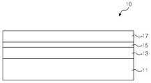
Translated fromKorean도 1은 종래의 (Al, Ga, In)N계 화합물 반도체의 개략적 종단면도이다.1 is a schematic longitudinal cross-sectional view of a conventional (Al, Ga, In) N-based compound semiconductor.
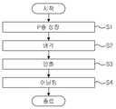
도 2는 종래의 (Al, Ga, In)N계 화합물 반도체의 P층 제조방법을 설명하는 순서도이다.FIG. 2 is a flowchart for explaining a P layer manufacturing method of a conventional (Al, Ga, In) N compound semiconductor.
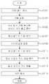
도 3은 본 발명의 바람직한 실시예에 따른 P형 화합물 반도체층 형성방법을 설명하기 위한 흐름도이다.3 is a flowchart illustrating a method of forming a P-type compound semiconductor layer according to a preferred embodiment of the present invention.
도 4는 본 발명의 바람직한 실시예에 따른 P형 화합물 반도체층 형성방법을 개략적으로 설명하기 위한 그래프이다.4 is a graph schematically illustrating a method of forming a P-type compound semiconductor layer according to a preferred embodiment of the present invention.
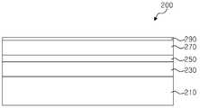
도 5는 본 발명의 바람직한 실시예에 따라 제조된 P형 화합물 반도체층을 구비하는 (Al, Ga, In)N계 화합물 반도체의 개략적 종 단면도이다.5 is a schematic longitudinal cross-sectional view of a (Al, Ga, In) N-based compound semiconductor having a P-type compound semiconductor layer prepared according to a preferred embodiment of the present invention.
본 발명은 P형 화합물 반도체층 형성방법에 관한 것으로서, 더욱 상세하게는 반도체 제조 공정을 단순화할 수 있는 P형 불순물을 포함하는 (Al,Ga,In)N계 화합물 반도체층(P층)의 형성방법에 관한 것이다.The present invention relates to a method of forming a P-type compound semiconductor layer, and more particularly, to the formation of a (Al, Ga, In) N-based compound semiconductor layer (P layer) containing a P-type impurity that can simplify the semiconductor manufacturing process. It is about a method.
(Al, Ga, In)N계 화합물 반도체는 예를 들어, 발광소자(Light Emitting Diode; LED) 또는 레이저소자(Laser Diode; LD)와 같은 화합물 반도체 소자에 응용된다. 도 1은 종래의 (Al,Ga,In)N계 화합물 반도체 소자를 개략적으로 나타낸 종단면도이다.The (Al, Ga, In) N-based compound semiconductors are applied to compound semiconductor devices such as, for example, light emitting diodes (LEDs) or laser diodes (LDs). 1 is a longitudinal sectional view schematically showing a conventional (Al, Ga, In) N-based compound semiconductor device.
도 1을 참조하면, 기판(11)상에 N형 불순물을 포함하는 (Al,Ga,In)N계 화합물 반도체층(N층, 13), 활성층(15) 및 P형 불순물을 포함하는 (Al,Ga,In)N계 화합물 반도체층(P층, 17)이 순차적으로 형성된다.Referring to FIG. 1, an (Al, Ga, In) N compound semiconductor layer (N layer, 13) containing an N-type impurity on the substrate 11 (N layer, 13), an
이러한 종래의 (Al, Ga, In)N계 화합물 반도체층은 금속유기화학기상증착법(Metaorganic Chemical Vapor Deposition: MOCVD) 등의 공정을 통해 성장된다.The conventional (Al, Ga, In) N-based compound semiconductor layer is grown through a process such as metalorganic chemical vapor deposition (MOCVD).
금속유기화학기상증착법에 따르면 (Al, Ga, In)N계 화합물 반도체층은, Al, Ga, 또는 In와 같은 III 족 원소의 소오스 가스, 수소와 질소를 함유한 암모니아(NH3) 가스가 반응챔버 내에 유입되고, 900~1200℃에서 상기 기판(11)상에 N층(13), 활성층(15) 및 P층(17)이 순차적으로 성장된다. 그리고, 마그네슘(Mg) 도핑 등으로 P층(17)이 형성되면 III 족 원소의 소오스 가스의 유입이 중단되고 암모니아의 유입은 유지되면서 반응챔버의 온도가 강하되어 기판(11)이 냉각된다.According to the metal organic chemical vapor deposition method, in the (Al, Ga, In) N compound semiconductor layer, a source gas of a group III element such as Al, Ga, or In, ammonia (NH3) gas containing hydrogen and nitrogen is a reaction chamber.
한편, 종래의 (Al,Ga,In)N계 화합물 반도체 소자(10)에서는 통상적으로, P층(17)에 예를 들어 마그네슘(Mg) 도핑 등으로 전도성을 확보한다. 그런데, 마그네슘(Mg)과 같은 P형 불순물은 상기한 바와 같은 반응챔버의 온도 강하 과정 중에 암모니아에 함유된 수소(H)와 쉽게 결합하게 되며, 이에 따라 P형 불순물의 자유정공을 제공하는 전자수용체(acceptor)로서의 기능이 저하되어 P형 화합물 반도체층의 저항값이 커지는 문제점이 있다.On the other hand, in the conventional (Al, Ga, In) N-based
따라서, (Al,Ga,In)N계 화합물 반도체의 P층 제조 공정에서는, P형 불순물과 수소의 결합을 떼어놓기 위해 별도의 어닐링 공정이 수행된다.Therefore, in the P-layer manufacturing process of the (Al, Ga, In) N-based compound semiconductor, a separate annealing process is performed to separate the bond between the P-type impurity and hydrogen.
도 2는 종래의 (Al,Ga,In)N계 화합물 반도체의 P층 제조방법을 설명하기 위한 순서도이다.2 is a flowchart for explaining a P layer manufacturing method of a conventional (Al, Ga, In) N-based compound semiconductor.
도 2를 참조하면, 반응챔버 내에서 기판의 온도를 900~1200℃로 상승시키고, P형 불순물, III 족 원소 및 암모니아를 공급하여 기판상에 화합물 반도체의 P층을 성장시킨다(S1). 상기 P층이 성장되면 P형 불순물과 III 족 원소의 소오스 가스의 공급을 중단하되 수소를 함유한 질소의 소오스 가스는 지속적으로 공급하며 반응챔버의 온도를 강하하여 기판을 상온으로 냉각시킨다(S2). 기판이 상온으로 냉각되면, 상기 P층이 성장된 기판을 반응챔버에서 인출하고(S3), 인출된 기판에 성장된 P층의 저항값을 낮추기 위해 어닐링 공정을 수행한다(S4). 미국 특허 US5,306,662호를 참조하면, P형 불순물, III 족 원소 및 암모니아로 화합물 반도체의 P층을 성장시킨 후, 400℃ 이상의 온도에서 상기 P층의 어닐링 공정을 수행한다. 그 결과, P층에 존재하는 P형 불순물에 결합된 수소가 제거되어, 저항값이 낮은 P형 (Al,Ga,In)N계 화합물 반도체가 제조된다.Referring to FIG. 2, the temperature of the substrate is raised to 900 to 1200 ° C. in the reaction chamber, and the P layer of the compound semiconductor is grown on the substrate by supplying P-type impurities, group III elements, and ammonia (S1). When the P layer is grown, supply of source gas of P-type impurities and group III elements is stopped, but source gas of nitrogen containing hydrogen is continuously supplied, and the temperature of the reaction chamber is lowered to cool the substrate to room temperature (S2). . When the substrate is cooled to room temperature, the substrate on which the P layer is grown is withdrawn from the reaction chamber (S3), and an annealing process is performed to lower the resistance value of the P layer grown on the extracted substrate (S4). Referring to US Pat. No. 5,306,662, a P layer of a compound semiconductor is grown with P-type impurities, Group III elements and ammonia, and then annealing of the P layer is performed at a temperature of 400 ° C or higher. As a result, hydrogen bonded to the P-type impurity present in the P layer is removed, thereby producing a P-type (Al, Ga, In) N-based compound semiconductor having a low resistance value.
이와 같이 종래의 (Al,Ga,In)N계 화합물 반도체 소자에서는, P층의 저항값을 낮추기 위해 적어도 한 번의 어닐링 공정을 추가하여 수행하여야 한다. 그러나, 이와 같이 추가적인 어닐링 공정은 화합물 반도체 소자의 제조 공정을 복잡하고 번거롭게 하는 문제가 있다.As described above, in the conventional (Al, Ga, In) N compound semiconductor device, at least one annealing process should be added to lower the resistance value of the P layer. However, this additional annealing process has a problem of complicated and cumbersome manufacturing process of the compound semiconductor device.
또한, 어닐링 공정의 추가에 따라 제품 제조에 소요되는 시간이 늘어나며, 특히 어닐링 공정을 위한 고가의 장비를 구입하여야 하고 장비설치를 위한 공간을 필요로 하는 등 제조설비를 위한 투자비용을 증가시켜, 제품의 단가를 상승시키는 요인이 된다.In addition, the time required for manufacturing the product increases with the addition of the annealing process, and in particular, the investment cost for the manufacturing equipment is increased by purchasing expensive equipment for the annealing process and requiring space for equipment installation. It is a factor that raises the unit price of.
한편, 종래 이와 같은 문제점을 해결하기 위해 반응챔버 내에서 900~1200℃의 온도에서 P층의 성장이 완료되면 P형 불순물, III 족 원소 및 암모니아의 공급을 중단하고 반응챔버의 온도를 강하하여 기판을 상온으로 냉각시키는 방법이 제안된 바 있다.On the other hand, in order to solve the conventional problem, when the growth of the P layer is completed in the reaction chamber at a temperature of 900 ~ 1200 ℃, the supply of P-type impurities, group III elements and ammonia is stopped and the temperature of the reaction chamber is lowered to the substrate It has been proposed to cool to room temperature.
그러나, 이 경우 성장된 P층으로부터 Al, Ga, In의 III족 원소와 질소가 분해되어 P층의 (Al, Ga, In)N 화합물 표면이 심하게 손상되는 문제점이 있다.However, in this case, Al, Ga, In group III elements and nitrogen are decomposed from the grown P layer, so that the (Al, Ga, In) N compound surface of the P layer is severely damaged.
본 발명이 이루고자 하는 기술적 과제는, P형 화합물 반도체층의 형성시 P형 불순물과 수소의 결합을 차단하고 P형 화합물 반도체층의 손상을 방지하는 P형 화합물 반도체층의 형성방법을 제공하는 데 있다.SUMMARY OF THE INVENTION The present invention has been made in an effort to provide a method of forming a P-type compound semiconductor layer that blocks the bonding of P-type impurities and hydrogen and prevents damage to the P-type compound semiconductor layer when the P-type compound semiconductor layer is formed. .
상기 기술적 과제들을 달성하기 위하여, 본 발명은 P형 화합물 반도체층 형성방법을 개시한다. 본 발명의 일 태양에 따른 P형 화합물 반도체층의 형성방법은, 반응챔버 내에 로딩된 기판을 제1 온도로 상승시키는 단계, 상기 반응챔버 내에 III 족 원소의 소오스 가스, P형 불순물의 소오스 가스, 및 수소를 함유하는 질소의 소오스 가스를 공급하여 P형 화합물 반도체층을 성장시키는 단계, 상기 P형 화 합물 반도체층의 성장이 완료된 후, 상기 III 족 원소의 소오스 가스 및 상기 P형 불순물의 소오스 가스들의 공급을 중단하고, 상기 기판의 온도를 제2 온도로 냉각시키는 단계, 상기 제2 온도에서 상기 III 족 원소의 소오스 가스, n형 또는 P형 불순물의 소오스 가스 및 상기 수소를 함유하는 질소의 소오스 가스를 공급하여 ITO 터널층을 성장시키는 단계, 및 상기 ITO 터널층의 성장이 완료되면 상기 III 족 원소의 소오스 가스, 상기 n형 또는 P형 불순물의 소오스 가스 및 상기 수소를 함유하는 질소의 소오스 가스을 중단하고 상기 기판 온도를 상온으로 냉각시키는 단계를 포함한다.In order to achieve the above technical problem, the present invention discloses a method for forming a P-type compound semiconductor layer. According to one or more exemplary embodiments, a method of forming a P-type compound semiconductor layer includes raising a substrate loaded in a reaction chamber to a first temperature, a source gas of a group III element, a source gas of a P-type impurity, And growing a P-type compound semiconductor layer by supplying a source gas of hydrogen containing nitrogen, and after completion of growth of the P-type compound semiconductor layer, a source gas of the Group III element and a source gas of the P-type impurity Suspending the supply of water and cooling the temperature of the substrate to a second temperature, the source gas of the Group III element, the source gas of n-type or P-type impurity and the source of nitrogen containing hydrogen at the second temperature Supplying a gas to grow the ITO tunnel layer, and when the growth of the ITO tunnel layer is completed, source gas of the group III element, n-type or P-type impurities Agarose gas and suspended gaseueul source of nitrogen containing the hydrogen, and including the step of cooling the substrate to room temperature.
여기서, 상기 제2 온도는 400 내지 900℃인 것이 바람직하다.Here, the second temperature is preferably 400 to 900 ° C.
또한, 상기 제2 온도에서 상기 ITO 터널층 성장이 완료되면 기설정된 시간동안 상기 제2 온도를 유지하는 단계를 더 포함하는 것이 더욱 바람직하다.The method may further include maintaining the second temperature for a predetermined time when the ITO tunnel layer growth is completed at the second temperature.
그리고, 상기 제2 온도에서 상기 ITO 터널층 성장이 완료되면 상기 반응챔버 내에 잔류하는 수소를 함유하는 질소의 소오스 가스를 배출하는 단계를 더 포함하는 것이 바람직하다.The method may further include discharging a source gas of nitrogen containing hydrogen remaining in the reaction chamber when the ITO tunnel layer growth is completed at the second temperature.
한편, 본 발명의 또다른 태양에 따른 P형 화합물 반도체층 형성방법은, 반응챔버 내에 로딩된 기판을 제1 온도로 상승시키고, 상기 반응챔버 내에 III 족 원소의 소오스 가스, P형 불순물의 소오스 가스, 및 수소를 함유하는 질소의 소오스 가스를 공급하여 P형 화합물 반도체층을 성장시킨다. 그리고, 상기 P형 화합물 반도체층의 성장이 완료된 후, 상기 III 족 원소의 소오스 가스 및 상기 P형 불순물의 소오스 가스들의 공급을 중단하고, 상기 기판의 온도를 제2 온도로 냉각시킨다. 이 어서, 상기 제2 온도에서 상기 III 족 원소의 소오스 가스, n형 또는 P형 불순물의 소오스 가스 및 상기 수소를 함유하는 질소의 소오스 가스를 공급하여 ITO 터널층을 성장시키고, 상기 ITO 터널층의 성장이 완료된 후, 상기 III 족 원소의 소오스 가스, 상기 n형 또는 P형 불순물의 소오스 가스의 공급을 중단한다. 이어서, 상기 기판의 온도를 제3 온도로 냉각시키고, 상기 수소를 함유하는 질소의 소오스 가스를 중단한 후 상기 기판 온도를 상온으로 냉각시킨다.On the other hand, the method for forming a P-type compound semiconductor layer according to another aspect of the present invention, by raising the substrate loaded in the reaction chamber to the first temperature, the source gas of the group III element, the source gas of the P-type impurities in the reaction chamber And a source gas of nitrogen containing hydrogen are supplied to grow the P-type compound semiconductor layer. After the growth of the P-type compound semiconductor layer is completed, supply of the source gas of the group III element and the source gas of the P-type impurity is stopped, and the temperature of the substrate is cooled to a second temperature. Then, at a second temperature, a source gas of the group III element, a source gas of n-type or P-type impurity, and a source gas of nitrogen containing hydrogen are supplied to grow an ITO tunnel layer, and After the growth is completed, the supply of the source gas of the group III element and the source gas of the n-type or P-type impurity is stopped. Subsequently, the temperature of the substrate is cooled to a third temperature, and the substrate temperature is cooled to room temperature after stopping the source gas of nitrogen containing hydrogen.
여기서, 상기 제3 온도는 400 내지 850℃이다.Here, the third temperature is 400 to 850 ℃.
이하, 첨부한 도면들을 참조하여 본 발명의 실시예들을 상세히 설명한다. 다음에 소개되는 실시예들은 당업자에게 본 발명의 사상이 충분히 전달될 수 있도록 하기 위해 예로서 제공되어지는 것이다. 따라서, 본 발명은 이하 설명된 실시예들에 한정되지 않고 다른 형태로 구체화될 수도 있다. 그리고, 도면들에 있어서, 구성요소의 폭, 길이, 두께 등은 편의를 위하여 과장되어 표현될 수도 있다. 명세서 전체에 걸쳐서 동일한 참조번호들은 동일한 구성요소들을 나타낸다.Hereinafter, with reference to the accompanying drawings will be described embodiments of the present invention; The following embodiments are provided as examples to sufficiently convey the spirit of the present invention to those skilled in the art. Accordingly, the invention is not limited to the embodiments described below and may be embodied in other forms. In the drawings, widths, lengths, thicknesses, and the like of components may be exaggerated for convenience. Like numbers refer to like elements throughout.
도 3은 본 발명의 바람직한 실시예에 따른 P형 반도체의 제조방법을 설명하기 위한 흐름도이고, 도 4는 본 발명의 바람직한 실시예에 따른 P형 반도체의 제조방법을 설명하기 위한 그래프이다.3 is a flowchart illustrating a method of manufacturing a P-type semiconductor according to a preferred embodiment of the present invention, and FIG. 4 is a graph illustrating a method of manufacturing a P-type semiconductor according to a preferred embodiment of the present invention.
본 발명의 바람직한 실시예에 따르면, III 족 원소의 질화물 반도체를 제조하기 위해 반응챔버 내에 기판을 로딩하고, 기판의 온도를 III 족 원소의 질화물 반도체층을 성장시키기 위한 온도(T1)로 상승시킨다(S101). III 족 원소의 질화물 반도체층을 성장시키기 위해 기판의 온도(T1)는 예를 들면 1050℃로 가열된다.According to a preferred embodiment of the present invention, a substrate is loaded into a reaction chamber to produce a nitride semiconductor of group III element, and the temperature of the substrate is raised to a temperature T1 for growing a nitride semiconductor layer of group III element. (S101). In order to grow the nitride semiconductor layer of the group III element, the temperature T1 of the substrate is heated to, for example, 1050 ° C.
기판으로는 절연성 재질의 사파이어(Sapphire)나 실리콘 카바이드(SiC) 등이 주로 사용되나 다른 전도성 또는 반도체 기판도 사용가능하다. 또한, 이러한 이종 기판과 III 족 원소의 질화물 반도체층 사이의 격자 부정합을 완화하기 위해 기판 위에 버퍼층이 형성되며, 생성된 버퍼층 위에 N형 불순물이 도핑된 III 족 원소의 질화물 반도체층, 즉 N형 반도체층과 활성층이 순차로 형성된다. 이러한 버퍼층은 AlN, InGaN, GaN, 또는 AlGaN 등으로 형성될 수 있다. 그리고, N형 반도체층은 불순물의 도핑 없이 형성할 수도 있지만, Si, Ge, Se, S, 또는 Te등의 불순물을 도핑하여 형성하는 것이 바람직하다.As the substrate, sapphire or silicon carbide (SiC) made of an insulating material is mainly used, but other conductive or semiconductor substrates may be used. In addition, a buffer layer is formed on the substrate to mitigate lattice mismatch between the dissimilar substrate and the nitride semiconductor layer of the group III element, and the nitride semiconductor layer of the group III element doped with the N type impurities on the resulting buffer layer, that is, the N type semiconductor. The layer and the active layer are formed sequentially. The buffer layer may be formed of AlN, InGaN, GaN, AlGaN, or the like. The N-type semiconductor layer may be formed without doping impurities, but is preferably formed by doping impurities such as Si, Ge, Se, S, or Te.
활성층은, 단일양자우물(SQW, Single Quantum Well) 또는 다중양자우물(MQW, Multi Quntum Well) 구조로 형성하는 것이 바람직하다.The active layer is preferably formed in a single quantum well (SQW, Single Quantum Well) or multi-quantum well (MQW, Multi Quntum Well) structure.
이어서, 반응챔버내로 III 족 원소의 소오스 가스와 P형 불순물의 소오스 가스 및 암모니아 등 수소를 함유하는 질소의 소오스 가스를 공급하여 P형 화합물 반도체층을 성장시킨다(S103). III 족 원소의 소오스 가스로는 예를 들어 트리메틸갈륨(Tri-Methyl Gallium: TMG), 질소(N)의 소오스 가스는 예를 들어 암모니아와 같은 수소를 함유하는 가스가 사용되며, 캐리어 가스(H2 또는 N2)와 함께 공급된다. 또한, P형 불순물의 소오스 가스로는, Mg을 불순물로 사용하는 경우 예를 들어 Cp2Mg (bis-cyclopentadienyl Mg)가 사용된다. P형 불순물로는 Mg 외에도 Be, Sr, Ba, Zn 등이 사용가능하다. 한편, 여기서는 N형 반도체층 위에 활성층을 형성하고, 활성층 위에 P형 화합물 반도체층을 성장시키는 것으로 기재하였으나 그 순서는 변경될 수 있다.Subsequently, a source gas of a group III element, a source gas of P-type impurities, and a source gas of nitrogen containing hydrogen, such as ammonia, are supplied into the reaction chamber to grow the P-type compound semiconductor layer (S103). As a source gas of Group III element, for example, Tri-Methyl Gallium (TGM) and a source gas of nitrogen (N) are used, for example, a gas containing hydrogen such as ammonia, and a carrier gas (H2 or Supplied with N2 ). As the source gas of the P-type impurity, when Mg is used as the impurity, for example, Cp2 Mg (bis-cyclopentadienyl Mg) is used. As the P-type impurity, Be, Sr, Ba, Zn, etc. may be used in addition to Mg. Meanwhile, although the active layer is formed on the N-type semiconductor layer and the P-type compound semiconductor layer is grown on the active layer, the order may be changed.
P형 화합물 반도체층의 성장이 완료되면, III 족 원소의 소오스 가스와 P형 불순물의 소오스 가스의 공급을 중단한다(S105). 그리고, P형 화합물 반도체층이 성장된 기판을 기설정된 온도(T2)로 냉각시킨다(S107).When the growth of the P-type compound semiconductor layer is completed, the supply of the source gas of the group III element and the source gas of the P-type impurity is stopped (S105). The substrate on which the P-type compound semiconductor layer is grown is cooled to a predetermined temperature (T2 ) (S107).
기판이 기설정된 온도(T2)로 냉각되면 III족 원소의 소오스 가스와 n형 또는 P형 불순물의 소오스 가스 및 수소를 함유하는 질소의 소오스가스를 공급하여 ITO 터널층을 성장시킨다(S109). ITO 터널층은 P형 화합물 반도체층과 그 위에 형성되는 ITO 투명전극층의 오믹 콘택을 위해 형성되며 ITO 투명전극층과 P형 화합물 반도체층 사이의 전기저항 및 이에 따른 의도치 않은 계면 발열을 줄일 수 있다. ITO 터널층은 (Al, Ga, In)N 계열의 반도체층으로 n형 또는 P형 불순물을 고농도로 도핑하여 형성될 수 있다.When the substrate is cooled to a predetermined temperature T2 , the ITO tunnel layer is grown by supplying a source gas of a group III element, a source gas of n-type or P-type impurities, and a source gas of nitrogen containing hydrogen (S109). The ITO tunnel layer is formed for ohmic contact between the P-type compound semiconductor layer and the ITO transparent electrode layer formed thereon, and can reduce electrical resistance between the ITO transparent electrode layer and the P-type compound semiconductor layer and thus undesired interfacial heat generation. The ITO tunnel layer is a (Al, Ga, In) N-based semiconductor layer and may be formed by high doping of n-type or P-type impurities.
한편, ITO 터널층의 성장 온도는 400 내지 900℃의 온도 범위이므로 상기한 P형 화합물 반도체층의 냉각 온도(T2)는 이러한 범위내에서 설정될 수 있다. ITO 터널층의 성장이 완료되면 III족 원소의 소오스 가스와 n형 또는 P형 불순물의 소오스 가스의 공급은 중단한다.On the other hand, since the growth temperature of the ITO tunnel layer is a temperature range of 400 to 900 ° C, the cooling temperature T2 of the P-type compound semiconductor layer may be set within this range. When the growth of the ITO tunnel layer is completed, supply of the source gas of the group III element and the source gas of the n-type or P-type impurity is stopped.
이어서, 기판을 기설정된 온도(T3)로 냉각시키고(S111), 수소를 함유하는 질소의 소오스 가스의 공급을 중단하고(S113), 반응챔버 내에 잔류하는 수소를 함유한 질소의 소오스 가스를 외부로 배출시킨다(S114). P형 화합물 반도체층이 냉각되 고 수소를 함유하는 질소의 소오스 가스의 공급이 중단되는 온도(T3)는 본 발명에서는 P형 화합물 반도체층의 P형 불순물과 수소의 결합이 이루어지지 않는 고온으로 설정되며, 이에 따라 P형 화합물 반도체층의 냉각 단계가 수행되는 동안 P형 불순물과 질소의 소오스 가스에 함유된 수소의 결합이 방지되므로, 형성된 P형 화합물 반도체층에서 수소를 제거하기 위한 별도의 어닐링 공정을 수행할 필요가 없게 된다.Subsequently, the substrate is cooled to a predetermined temperature (T3 ) (S111), the supply of source gas of nitrogen containing hydrogen is stopped (S113), and the source gas of nitrogen containing hydrogen remaining in the reaction chamber is externally supplied. To discharge (S114). The temperature (T3 ) at which the P-type compound semiconductor layer is cooled and supply of hydrogen-containing nitrogen gas is stopped (T3 ) is a high temperature at which the P-type impurity and hydrogen of the P-type compound semiconductor layer are not bonded. In this way, since the bonding of P-type impurities and hydrogen contained in the source gas of nitrogen is prevented during the cooling step of the P-type compound semiconductor layer, a separate annealing for removing hydrogen from the formed P-type compound semiconductor layer is prevented. There is no need to perform the process.
여기서, P형 화합물 반도체층의 냉각시켜 수소를 함유한 질소의 소오스 가스의 공급을 중단하는 온도(T3)는, 예를 들면 400 내지 850℃의 온도 범위에서 설정된다. 400℃ 이하의 온도에서는 수소와 마그네슘의 결합이 발생할 수 있으므로 400℃ 이하에서 암모니아 등의 수소를 함유하는 질소의 소오스 가스를 중단하는 것은 바람직하지 않다.Here, the temperature T3 at which the P-type compound semiconductor layer is cooled and the supply of hydrogen-containing nitrogen source gas is interrupted is set, for example, in a temperature range of 400 to 850 ° C. It is not preferable to stop the source gas of nitrogen containing hydrogen, such as ammonia, at 400 degrees C or less, since the coupling | bonding of hydrogen and magnesium may occur at the temperature below 400 degrees C.
한편, 상기한 ITO 터널층의 성장 온도(T2)를 수소를 함유한 질소의 소오스 가스의 공급 중단 단계 수행 온도(T3)와 일치시켜, ITO 터널층의 성장이 완료되면 수소를 함유한 질소의 소오스 가스의 공급을 중단하고, 가스가 반응챔버로부터 배출될 때까지 상기 온도(T2)를 유지한 후 기판을 냉각할 수도 있다.On the other hand, the growth temperature (T2 ) of the ITO tunnel layer is matched with the execution temperature (T3 ) of the supply interruption step of supplying the source gas of nitrogen containing hydrogen, and when the growth of the ITO tunnel layer is completed, nitrogen containing hydrogen The supply of the source gas may be stopped and the substrate may be cooled after the temperature T2 is maintained until the gas is discharged from the reaction chamber.
도 4a를 참조하면, ITO 터널층은 기설정된 온도(T2)에서 수행되고, 이후 기판이 기설정된 온도(T3)로 냉각되면 수소를 함유하는 질소의 소오스 가스의 배출 단계가 소정의 시간 간격(P4 에서 P5) 동안 수행되며, 이러한 시간 간격(P2 에서 P3) 동안 기판의 온도(T2)는 동일하게 유지된다. 이는, 기판의 온도를 적어도 반응챔버 내에 잔존하는 수소를 함유하는 질소 소오스 가스에 함유된 수소와 P형 화합물 반도체층의 P형 불순물 간의 결합 반응을 차단할 수 있는 온도 이상으로 유지하기 위함이며, 반드시 동일한 온도로 유지하여야 하는 것은 아니다.Referring to FIG. 4A, the ITO tunnel layer is performed at a predetermined temperature T2 , and thereafter, when the substrate is cooled to the predetermined temperature T3 , the step of discharging the source gas of nitrogen containing hydrogen is a predetermined time interval. (P4 to P5 ), the temperature T2 of the substrate remains the same during this time interval P2 to P3 . This is to maintain the temperature of the substrate at a temperature that can at least prevent the coupling reaction between hydrogen contained in the nitrogen source gas containing hydrogen remaining in the reaction chamber and P-type impurities in the P-type compound semiconductor layer. It is not necessary to maintain the temperature.
한편, 도 4b는 ITO 터널층의 성장 온도(T2)와 수소가 함유된 질소의 소오스 가스의 공급 중단 온도(T3)를 일치시킨 경우의 예로서 ITO 터널층의 성장이 일정 시간(P2 에서 P6) 동안 수행된 후 수소를 함유하는 질소의 소오스 가스의 공급을 중단하고 잔류 가스가 반응챔버에서 배출될 때까지 일정 시간(P6 에서 P7) 동안 동일한 온도(T2)가 유지된다.On the other hand, Figure 4b is an example of a case where the growth temperature (T2 ) of the ITO tunnel layer and the supply stop temperature (T3 ) of the source gas of nitrogen containing hydrogen is coincident with the growth of the ITO tunnel layer for a predetermined time (P2). At P6 ), then the supply of hydrogen containing nitrogen source gas is stopped and the same temperature (T2 ) is maintained for a period of time (P6 to P7 ) until residual gas is discharged from the reaction chamber. .
수소를 함유하는 질소 소오스 가스의 공급이 중단되고 반응챔버 내로 잔존하는 수소를 함유하는 질소 소오스 가스가 외부로 배출되면(도 4a의 P5 시점 또는 도 4b의 P7 시점), 기판의 온도를 반응챔버 내에서 인출할 수 있을 정도까지, 예를 들어 상온으로 냉각시킨다(S115). 이 경우, 질소 가스를 냉각 가스로 사용할 수도 있다.When the supply of the nitrogen source gas containing hydrogen is stopped and the nitrogen source gas containing hydrogen remaining in the reaction chamber is discharged to the outside (time point P5 of FIG. 4A or time point P7 of FIG. 4B), the temperature of the substrate is reacted. To the extent that it can be taken out in the chamber, for example, cooled to room temperature (S115). In this case, nitrogen gas may be used as the cooling gas.
도 5는 본 발명의 바람직한 실시예에 따라 제조된 P형 반도체를 구비하는 (Al, Ga, In)N계 화합물 반도체의 개략적 종 단면도이다.5 is a schematic longitudinal cross-sectional view of a (Al, Ga, In) N-based compound semiconductor having a P-type semiconductor manufactured according to a preferred embodiment of the present invention.
본 실시예에 따른 (Al,Ga,In)N계 화합물 반도체(200)에서는, 기판(210)위에 N층(230), 활성층(250), P층(270) 및 ITO 터널층(290)이 형성되어 있다. 기판(210) 은, 도전성 또는 반도전성의 금속, Si, SiC, 또는 GaN 등으로 형성될 수 있으며, 그 자체로 N형 전극으로서의 기능을 수행할 수 있다. 기판(210)은 또한 사파이어 또는 스피넬로 형성될 수 있다. N층(230)과 기판(210) 사이에는 전술한 바와 같이 버퍼층(미도시)을 형성할 수 있다.In the (Al, Ga, In)
본 실시예에 있어서, P형 화합물 반도체층인 P층(270)은 도 3을 참조하여 전술한 바와 같이, 어닐링 공정 없이 형성된다. 이를 위해, 반응챔버 내에서 P층(270)의 성장이 완료되면, III 족 원소의 소오스 가스와 P형 불순물의 소오스 가스 공급을 중단하고, P형 화합물 반도체층이 성장된 기판을 기설정된 온도(T2)로 냉각시킨 후 ITO 터널층(290)을 성장시킨 후 전술한 바와 같이 동일 온도(T2)에서 또는 기설정된 온도(T3)로 냉각한 후 수소를 함유한 질소 소오스 가스의 공급을 중단한다. 여기서, ITO 터널층(290) 성장 온도(T2)는, 예를 들면 400 내지 900℃의 온도 범위에서 설정되고 수소를 함유한 질소의 소오스 가스 공급 중단 온도(T3)는 400 내지 850℃에서 설정된다. 따라서, 두 가지의 온도를 일치시켜 ITO 터널층(290)의 성장이 완료되면 수소를 함유한 질소의 소오스 가스의 공급을 중단하고 일정 시간 온도를 유지한 후 기판을 냉각할 수도 있다. 이어서, 반응챔버 내에 잔존하는 수소를 함유하는 질소 소오스 가스가 외부로 방출되면, 기판의 온도를 반응챔버 내에서 인출할 수 있을 정도로 냉각시킨다. 이와 같이 형성된 P형 화합물 반도체층은 수소와 결합되지 않은 P형 불순물을 포함하며, 이에 따라 수소를 제거하기 위한 별도의 어 닐링 공정을 수행할 필요가 없다.In this embodiment, the
한편, 도 5에는 기판(210)이 N층(230)에 인접하게 배치된 실시예에 대해서 설명하였지만, 본 발명은 이에 국한되지 아니하고, 기판이 P층에 인접하게 배치된 구성에도 적용가능하다. 이러한 구성에서도, 상술한 및 도시한 실시예와 마찬가지의 동일 기능 및 효과가 제공된다.Meanwhile, although the embodiment in which the
그리고, 본 발명과 관련하여 전 부분에서 설명되고 있는 (Al,Ga,In)N계 화합물 반도체는, AlxInyGa1-x-yN(0≤x, y, x+y≤1)를 포함하는 것임은 물론이며, 이러한 화합물 반도체는 예를 들어, 발광소자(LED, Light Emitting Diode), 레이저소자(LD, Laser Diode), 이종접합 바이폴라 트랜지스터, 전계효과 트랜지스터, 또는 광감지기(photodetector) 이외에 다양한 분야에 적용가능하다.And, which it is described in the former part (Al, Ga, In) N-based compound semiconductor, Alx Iny Ga1-x-y N (0≤x, y, x + y≤1) in accordance with the present invention; Of course, the compound semiconductor may include, for example, a light emitting diode (LED), a laser diode (LD), a heterojunction bipolar transistor, a field effect transistor, or a photodetector. In addition, it is applicable to various fields.
본 발명의 실시예들에 따르면, P형 화합물 반도체층의 형성시 P형 불순물과 수소의 결합을 적절하게 차단할 수 있어 별도의 어닐링 공정을 수행할 필요가 없으며, 어닐링 공정 없이도 저항값이 낮은 P형 화합물 반도체를 제조할 수 있는 P형 반도체 제조방법을 제공할 수 있다.According to the exemplary embodiments of the present invention, the formation of the P-type compound semiconductor layer may appropriately block the bonding of the P-type impurity and hydrogen, and thus, there is no need to perform a separate annealing process, and P-type having low resistance even without the annealing process. It is possible to provide a P-type semiconductor manufacturing method capable of manufacturing a compound semiconductor.
또한, P형 화합물 반도체층의 제조 공정과 함께 그 냉각 과정에서 동일한 챔버 내에서 ITO 터널층을 제조함으로써, 종래의 P형 반도체 제조방법에서 수행되는 어닐링 공정을 생략할 수 있을 뿐만 아니라 화합물 반도체 소자의 제조 공정을 단순화하고, 제조에 소요되는 시간을 단축할 수 있다.In addition, by manufacturing the ITO tunnel layer in the same chamber during the cooling process together with the manufacturing process of the P-type compound semiconductor layer, not only the annealing process performed in the conventional P-type semiconductor manufacturing method can be omitted, The manufacturing process can be simplified and the time required for manufacturing can be shortened.
또한, P형 반도체층을 형성한 후 기판을 기설정된 온도로 냉각시킨 후 ITO 터널층을 형성하고 수소를 함유하는 질소 소오스 가스의 공급을 중단한 후 기판을 냉각함으로써 결정체의 손상을 방지할 수 있다.In addition, after the P-type semiconductor layer is formed, the substrate is cooled to a predetermined temperature, the ITO tunnel layer is formed, the supply of hydrogen-containing nitrogen source gas is stopped, and the substrate is cooled, thereby preventing damage to crystals. .
Claims (8)
Translated fromKoreanPriority Applications (7)
| Application Number | Priority Date | Filing Date | Title |
|---|---|---|---|
| KR1020060060820AKR100707798B1 (en) | 2006-06-30 | 2006-06-30 | P-type compound semiconductor layer formation method |
| PCT/KR2007/003185WO2008002104A1 (en) | 2006-06-30 | 2007-06-29 | Method of forming p-type compound semiconductor layer |
| US12/090,305US7682953B2 (en) | 2006-06-30 | 2007-06-29 | Method of forming p-type compound semiconductor layer |
| DE112007000059TDE112007000059T5 (en) | 2006-06-30 | 2007-06-29 | A method of forming a compound semiconductor layer of P-type |
| JP2009517985AJP2009543331A (en) | 2006-06-30 | 2007-06-29 | Method for forming p-type compound semiconductor layer |
| US12/560,891US8470697B2 (en) | 2006-06-30 | 2009-09-16 | Method of forming p-type compound semiconductor layer |
| JP2012223419AJP5947183B2 (en) | 2006-06-30 | 2012-10-05 | Method for forming p-type compound semiconductor layer |
Applications Claiming Priority (1)
| Application Number | Priority Date | Filing Date | Title |
|---|---|---|---|
| KR1020060060820AKR100707798B1 (en) | 2006-06-30 | 2006-06-30 | P-type compound semiconductor layer formation method |
Publications (1)
| Publication Number | Publication Date |
|---|---|
| KR100707798B1true KR100707798B1 (en) | 2007-04-18 |
Family
ID=38181437
Family Applications (1)
| Application Number | Title | Priority Date | Filing Date |
|---|---|---|---|
| KR1020060060820AExpired - Fee RelatedKR100707798B1 (en) | 2006-06-30 | 2006-06-30 | P-type compound semiconductor layer formation method |
Country Status (1)
| Country | Link |
|---|---|
| KR (1) | KR100707798B1 (en) |
Citations (4)
| Publication number | Priority date | Publication date | Assignee | Title |
|---|---|---|---|---|
| KR20010001123A (en)* | 1999-06-02 | 2001-01-05 | 조장연 | Fabrication of GaN Semiconductor Light Emitting Device |
| JP2001119065A (en) | 1999-10-15 | 2001-04-27 | Matsushita Electric Ind Co Ltd | P-type nitride semiconductor and method of manufacturing the same |
| KR20050025054A (en)* | 2003-09-03 | 2005-03-11 | 삼성전기주식회사 | AlGaInN based P-N Diode and Fabrication Method thereof |
| JP2006140530A (en) | 2006-01-23 | 2006-06-01 | Matsushita Electric Ind Co Ltd | Method for manufacturing p-type nitride semiconductor |
- 2006
- 2006-06-30KRKR1020060060820Apatent/KR100707798B1/ennot_activeExpired - Fee Related
Patent Citations (4)
| Publication number | Priority date | Publication date | Assignee | Title |
|---|---|---|---|---|
| KR20010001123A (en)* | 1999-06-02 | 2001-01-05 | 조장연 | Fabrication of GaN Semiconductor Light Emitting Device |
| JP2001119065A (en) | 1999-10-15 | 2001-04-27 | Matsushita Electric Ind Co Ltd | P-type nitride semiconductor and method of manufacturing the same |
| KR20050025054A (en)* | 2003-09-03 | 2005-03-11 | 삼성전기주식회사 | AlGaInN based P-N Diode and Fabrication Method thereof |
| JP2006140530A (en) | 2006-01-23 | 2006-06-01 | Matsushita Electric Ind Co Ltd | Method for manufacturing p-type nitride semiconductor |
Similar Documents
| Publication | Publication Date | Title |
|---|---|---|
| WO2007083647A1 (en) | Nitride semiconductor light-emitting device | |
| US20110177678A1 (en) | Method for manufacturing nitride semiconductor device | |
| JP2002231997A (en) | Nitride based semiconductor light emitting device | |
| JP3740744B2 (en) | Semiconductor growth method | |
| JP5947183B2 (en) | Method for forming p-type compound semiconductor layer | |
| JP3603598B2 (en) | Method for manufacturing group 3-5 compound semiconductor | |
| JP2004134750A (en) | Method for producing p-type group III nitride compound semiconductor | |
| JP2010534933A (en) | Semiconductor light emitting device and manufacturing method thereof | |
| JP3773713B2 (en) | Method for forming quantum box | |
| KR101261629B1 (en) | Method for fabricating a compound semiconductor device | |
| JP3741528B2 (en) | Method for manufacturing gallium nitride based semiconductor device | |
| CN101868848B (en) | Method for fabricating p-type gallium nitride-based semiconductor, method for fabricating nitride-based semiconductor element, and method for fabricating epitaxial wafer | |
| JP3497790B2 (en) | Method for manufacturing p-type gallium nitride based semiconductor and light emitting device using p-type gallium nitride based semiconductor | |
| US6225195B1 (en) | Method for manufacturing group III-V compound semiconductor | |
| JP4284944B2 (en) | Method for manufacturing gallium nitride based semiconductor laser device | |
| JP2003178987A (en) | Method for manufacturing nitride-based compound semiconductor, nitride-based compound semiconductor wafer, and nitride-based compound semiconductor device | |
| JP4609917B2 (en) | Method for producing aluminum gallium nitride layer, method for producing group III nitride semiconductor light emitting device, and group III nitride semiconductor light emitting device | |
| JP4200115B2 (en) | Carbon-doped semiconductor film, semiconductor element, and manufacturing method thereof | |
| KR100707798B1 (en) | P-type compound semiconductor layer formation method | |
| EP1772909B1 (en) | (AI,Ga,In)N-Based compound semiconductor and method of fabricating the same | |
| KR100737820B1 (en) | P-type compound semiconductor layer formation method | |
| KR100757801B1 (en) | P-type compound semiconductor layer formation method | |
| JP4829273B2 (en) | Group III nitride semiconductor light emitting device manufacturing method | |
| JP3557875B2 (en) | GaN-based semiconductor device and method of manufacturing the same | |
| KR101186681B1 (en) | P-LAYER OF A GaN BASED COMPOUND SEMICONDUCTOR AND METHOD OF FABRICATING THE SAME |
Legal Events
| Date | Code | Title | Description |
|---|---|---|---|
| A201 | Request for examination | ||
| PA0109 | Patent application | St.27 status event code:A-0-1-A10-A12-nap-PA0109 | |
| PA0201 | Request for examination | St.27 status event code:A-1-2-D10-D11-exm-PA0201 | |
| D13-X000 | Search requested | St.27 status event code:A-1-2-D10-D13-srh-X000 | |
| D14-X000 | Search report completed | St.27 status event code:A-1-2-D10-D14-srh-X000 | |
| E701 | Decision to grant or registration of patent right | ||
| PE0701 | Decision of registration | St.27 status event code:A-1-2-D10-D22-exm-PE0701 | |
| GRNT | Written decision to grant | ||
| PR0701 | Registration of establishment | St.27 status event code:A-2-4-F10-F11-exm-PR0701 | |
| PR1002 | Payment of registration fee | St.27 status event code:A-2-2-U10-U11-oth-PR1002 Fee payment year number:1 | |
| PG1601 | Publication of registration | St.27 status event code:A-4-4-Q10-Q13-nap-PG1601 | |
| P14-X000 | Amendment of ip right document requested | St.27 status event code:A-5-5-P10-P14-nap-X000 | |
| P16-X000 | Ip right document amended | St.27 status event code:A-5-5-P10-P16-nap-X000 | |
| Q16-X000 | A copy of ip right certificate issued | St.27 status event code:A-4-4-Q10-Q16-nap-X000 | |
| P22-X000 | Classification modified | St.27 status event code:A-4-4-P10-P22-nap-X000 | |
| PR1001 | Payment of annual fee | St.27 status event code:A-4-4-U10-U11-oth-PR1001 Fee payment year number:4 | |
| PR1001 | Payment of annual fee | St.27 status event code:A-4-4-U10-U11-oth-PR1001 Fee payment year number:5 | |
| PR1001 | Payment of annual fee | St.27 status event code:A-4-4-U10-U11-oth-PR1001 Fee payment year number:6 | |
| FPAY | Annual fee payment | Payment date:20130318 Year of fee payment:7 | |
| PR1001 | Payment of annual fee | St.27 status event code:A-4-4-U10-U11-oth-PR1001 Fee payment year number:7 | |
| R18-X000 | Changes to party contact information recorded | St.27 status event code:A-5-5-R10-R18-oth-X000 | |
| FPAY | Annual fee payment | Payment date:20140401 Year of fee payment:8 | |
| PR1001 | Payment of annual fee | St.27 status event code:A-4-4-U10-U11-oth-PR1001 Fee payment year number:8 | |
| R18-X000 | Changes to party contact information recorded | St.27 status event code:A-5-5-R10-R18-oth-X000 | |
| PN2301 | Change of applicant | St.27 status event code:A-5-5-R10-R13-asn-PN2301 St.27 status event code:A-5-5-R10-R11-asn-PN2301 | |
| PR1001 | Payment of annual fee | St.27 status event code:A-4-4-U10-U11-oth-PR1001 Fee payment year number:9 | |
| PR1001 | Payment of annual fee | St.27 status event code:A-4-4-U10-U11-oth-PR1001 Fee payment year number:10 | |
| FPAY | Annual fee payment | Payment date:20170308 Year of fee payment:11 | |
| PR1001 | Payment of annual fee | St.27 status event code:A-4-4-U10-U11-oth-PR1001 Fee payment year number:11 | |
| P22-X000 | Classification modified | St.27 status event code:A-4-4-P10-P22-nap-X000 | |
| PR1001 | Payment of annual fee | St.27 status event code:A-4-4-U10-U11-oth-PR1001 Fee payment year number:12 | |
| P22-X000 | Classification modified | St.27 status event code:A-4-4-P10-P22-nap-X000 | |
| LAPS | Lapse due to unpaid annual fee | ||
| PC1903 | Unpaid annual fee | St.27 status event code:A-4-4-U10-U13-oth-PC1903 Not in force date:20190410 Payment event data comment text:Termination Category : DEFAULT_OF_REGISTRATION_FEE | |
| PC1903 | Unpaid annual fee | St.27 status event code:N-4-6-H10-H13-oth-PC1903 Ip right cessation event data comment text:Termination Category : DEFAULT_OF_REGISTRATION_FEE Not in force date:20190410 | |
| P22-X000 | Classification modified | St.27 status event code:A-4-4-P10-P22-nap-X000 |