KR100707187B1 - Gallium Nitride Compound Semiconductor Device - Google Patents
Gallium Nitride Compound Semiconductor DeviceDownload PDFInfo
- Publication number
- KR100707187B1 KR100707187B1KR1020050033197AKR20050033197AKR100707187B1KR 100707187 B1KR100707187 B1KR 100707187B1KR 1020050033197 AKR1020050033197 AKR 1020050033197AKR 20050033197 AKR20050033197 AKR 20050033197AKR 100707187 B1KR100707187 B1KR 100707187B1
- Authority
- KR
- South Korea
- Prior art keywords
- gallium nitride
- compound semiconductor
- substrate
- nitride compound
- semiconductor device
- Prior art date
- Legal status (The legal status is an assumption and is not a legal conclusion. Google has not performed a legal analysis and makes no representation as to the accuracy of the status listed.)
- Expired - Fee Related
Links
Images


Classifications
- H—ELECTRICITY
- H01—ELECTRIC ELEMENTS
- H01L—SEMICONDUCTOR DEVICES NOT COVERED BY CLASS H10
- H01L21/00—Processes or apparatus adapted for the manufacture or treatment of semiconductor or solid state devices or of parts thereof
- H01L21/02—Manufacture or treatment of semiconductor devices or of parts thereof
- H01L21/04—Manufacture or treatment of semiconductor devices or of parts thereof the devices having potential barriers, e.g. a PN junction, depletion layer or carrier concentration layer
- H01L21/18—Manufacture or treatment of semiconductor devices or of parts thereof the devices having potential barriers, e.g. a PN junction, depletion layer or carrier concentration layer the devices having semiconductor bodies comprising elements of Group IV of the Periodic Table or AIIIBV compounds with or without impurities, e.g. doping materials
- H01L21/20—Deposition of semiconductor materials on a substrate, e.g. epitaxial growth solid phase epitaxy
- H—ELECTRICITY
- H10—SEMICONDUCTOR DEVICES; ELECTRIC SOLID-STATE DEVICES NOT OTHERWISE PROVIDED FOR
- H10D—INORGANIC ELECTRIC SEMICONDUCTOR DEVICES
- H10D62/00—Semiconductor bodies, or regions thereof, of devices having potential barriers
- H10D62/80—Semiconductor bodies, or regions thereof, of devices having potential barriers characterised by the materials
- H10D62/85—Semiconductor bodies, or regions thereof, of devices having potential barriers characterised by the materials being Group III-V materials, e.g. GaAs
- H10D62/8503—Nitride Group III-V materials, e.g. AlN or GaN
- B—PERFORMING OPERATIONS; TRANSPORTING
- B82—NANOTECHNOLOGY
- B82Y—SPECIFIC USES OR APPLICATIONS OF NANOSTRUCTURES; MEASUREMENT OR ANALYSIS OF NANOSTRUCTURES; MANUFACTURE OR TREATMENT OF NANOSTRUCTURES
- B82Y20/00—Nanooptics, e.g. quantum optics or photonic crystals
- H—ELECTRICITY
- H01—ELECTRIC ELEMENTS
- H01S—DEVICES USING THE PROCESS OF LIGHT AMPLIFICATION BY STIMULATED EMISSION OF RADIATION [LASER] TO AMPLIFY OR GENERATE LIGHT; DEVICES USING STIMULATED EMISSION OF ELECTROMAGNETIC RADIATION IN WAVE RANGES OTHER THAN OPTICAL
- H01S5/00—Semiconductor lasers
- H01S5/30—Structure or shape of the active region; Materials used for the active region
- H01S5/34—Structure or shape of the active region; Materials used for the active region comprising quantum well or superlattice structures, e.g. single quantum well [SQW] lasers, multiple quantum well [MQW] lasers or graded index separate confinement heterostructure [GRINSCH] lasers
- H01S5/343—Structure or shape of the active region; Materials used for the active region comprising quantum well or superlattice structures, e.g. single quantum well [SQW] lasers, multiple quantum well [MQW] lasers or graded index separate confinement heterostructure [GRINSCH] lasers in AIIIBV compounds, e.g. AlGaAs-laser, InP-based laser
- H01S5/34333—Structure or shape of the active region; Materials used for the active region comprising quantum well or superlattice structures, e.g. single quantum well [SQW] lasers, multiple quantum well [MQW] lasers or graded index separate confinement heterostructure [GRINSCH] lasers in AIIIBV compounds, e.g. AlGaAs-laser, InP-based laser with a well layer based on Ga(In)N or Ga(In)P, e.g. blue laser
- H—ELECTRICITY
- H10—SEMICONDUCTOR DEVICES; ELECTRIC SOLID-STATE DEVICES NOT OTHERWISE PROVIDED FOR
- H10D—INORGANIC ELECTRIC SEMICONDUCTOR DEVICES
- H10D62/00—Semiconductor bodies, or regions thereof, of devices having potential barriers
- H10D62/40—Crystalline structures
- H10D62/405—Orientations of crystalline planes
- H—ELECTRICITY
- H10—SEMICONDUCTOR DEVICES; ELECTRIC SOLID-STATE DEVICES NOT OTHERWISE PROVIDED FOR
- H10H—INORGANIC LIGHT-EMITTING SEMICONDUCTOR DEVICES HAVING POTENTIAL BARRIERS
- H10H20/00—Individual inorganic light-emitting semiconductor devices having potential barriers, e.g. light-emitting diodes [LED]
- H10H20/80—Constructional details
- H10H20/81—Bodies
- H10H20/817—Bodies characterised by the crystal structures or orientations, e.g. polycrystalline, amorphous or porous
- H—ELECTRICITY
- H10—SEMICONDUCTOR DEVICES; ELECTRIC SOLID-STATE DEVICES NOT OTHERWISE PROVIDED FOR
- H10H—INORGANIC LIGHT-EMITTING SEMICONDUCTOR DEVICES HAVING POTENTIAL BARRIERS
- H10H20/00—Individual inorganic light-emitting semiconductor devices having potential barriers, e.g. light-emitting diodes [LED]
- H10H20/80—Constructional details
- H10H20/81—Bodies
- H10H20/822—Materials of the light-emitting regions
- H10H20/824—Materials of the light-emitting regions comprising only Group III-V materials, e.g. GaP
- H10H20/825—Materials of the light-emitting regions comprising only Group III-V materials, e.g. GaP containing nitrogen, e.g. GaN
- H—ELECTRICITY
- H01—ELECTRIC ELEMENTS
- H01S—DEVICES USING THE PROCESS OF LIGHT AMPLIFICATION BY STIMULATED EMISSION OF RADIATION [LASER] TO AMPLIFY OR GENERATE LIGHT; DEVICES USING STIMULATED EMISSION OF ELECTROMAGNETIC RADIATION IN WAVE RANGES OTHER THAN OPTICAL
- H01S5/00—Semiconductor lasers
- H01S5/02—Structural details or components not essential to laser action
- H01S5/0206—Substrates, e.g. growth, shape, material, removal or bonding
- H01S5/0207—Substrates having a special shape
- H—ELECTRICITY
- H01—ELECTRIC ELEMENTS
- H01S—DEVICES USING THE PROCESS OF LIGHT AMPLIFICATION BY STIMULATED EMISSION OF RADIATION [LASER] TO AMPLIFY OR GENERATE LIGHT; DEVICES USING STIMULATED EMISSION OF ELECTROMAGNETIC RADIATION IN WAVE RANGES OTHER THAN OPTICAL
- H01S5/00—Semiconductor lasers
- H01S5/02—Structural details or components not essential to laser action
- H01S5/0206—Substrates, e.g. growth, shape, material, removal or bonding
- H01S5/0211—Substrates made of ternary or quaternary compounds
- H—ELECTRICITY
- H01—ELECTRIC ELEMENTS
- H01S—DEVICES USING THE PROCESS OF LIGHT AMPLIFICATION BY STIMULATED EMISSION OF RADIATION [LASER] TO AMPLIFY OR GENERATE LIGHT; DEVICES USING STIMULATED EMISSION OF ELECTROMAGNETIC RADIATION IN WAVE RANGES OTHER THAN OPTICAL
- H01S5/00—Semiconductor lasers
- H01S5/20—Structure or shape of the semiconductor body to guide the optical wave ; Confining structures perpendicular to the optical axis, e.g. index or gain guiding, stripe geometry, broad area lasers, gain tailoring, transverse or lateral reflectors, special cladding structures, MQW barrier reflection layers
- H01S5/22—Structure or shape of the semiconductor body to guide the optical wave ; Confining structures perpendicular to the optical axis, e.g. index or gain guiding, stripe geometry, broad area lasers, gain tailoring, transverse or lateral reflectors, special cladding structures, MQW barrier reflection layers having a ridge or stripe structure
- H01S5/223—Buried stripe structure
- H01S5/2231—Buried stripe structure with inner confining structure only between the active layer and the upper electrode
Landscapes
- Physics & Mathematics (AREA)
- Engineering & Computer Science (AREA)
- Optics & Photonics (AREA)
- Chemical & Material Sciences (AREA)
- Nanotechnology (AREA)
- General Physics & Mathematics (AREA)
- Condensed Matter Physics & Semiconductors (AREA)
- Crystallography & Structural Chemistry (AREA)
- Biophysics (AREA)
- Electromagnetism (AREA)
- Life Sciences & Earth Sciences (AREA)
- Manufacturing & Machinery (AREA)
- Computer Hardware Design (AREA)
- Microelectronics & Electronic Packaging (AREA)
- Power Engineering (AREA)
- Semiconductor Lasers (AREA)
- Led Devices (AREA)
- Light Receiving Elements (AREA)
Abstract
Translated fromKoreanDescription
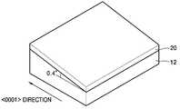
Translated fromKorean도 1은 본 발명의 제1실시예에 따른 질화갈륨계 화합물 반도체 소자의 개략적 사시도이다.1 is a schematic perspective view of a gallium nitride compound semiconductor device according to a first embodiment of the present invention.
도 2는 도 1의 상세도이다.2 is a detailed view of FIG. 1.
도 3a 내지 도 3c는 각각의 표면 경사각(surface off angle)에 따라 기판 위에 성장되는 박막의 표면형상을 보여주는 광학 간섭현미경 사진이다.3A to 3C are optical coherence micrographs showing the surface shape of a thin film grown on a substrate according to each surface off angle.
도 4는 본 발명의 제1실시예에 따른 질화갈륨계 화합물 반도체 소자를 이용한 레이저 다이오드(LD;Laser Diode)의 개략적 사시도이다.4 is a schematic perspective view of a laser diode (LD) using a gallium nitride compound semiconductor device according to a first embodiment of the present invention.
도 5는 본 발명의 제2실시예에 따른 질화갈륨계 화합물 반도체 소자의 개략적 사시도이다.5 is a schematic perspective view of a gallium nitride compound semiconductor device according to a second embodiment of the present invention.
도 6은 도 5의 상세도이다.6 is a detailed view of FIG. 5.
< 도면의 주요부분에 대한 부호의 설명 ><Description of Symbols for Major Parts of Drawings>
11, 12:n-형 AlxInyGa1-x-yN 기판 20:질화갈륨계 화합물 반도체층11, 12: n-type Alx Iny Ga1-xy N substrate 20: gallium nitride compound semiconductor layer
21:n-형 클래딩층 22:n-형 광도파층21: n-type cladding layer 22: n-type optical waveguide layer
23:다중양자우물 활성층 24:p-형 광도파층23: multi-quantum well active layer 24: p-type optical waveguide layer
25:p-형 클래딩층 26:p-형 콘택트층25: p-type cladding layer 26: p-type contact layer
27:보호절연층 28:p-측 전극27: protective insulating layer 28: p-side electrode
31:n-측 전극31: n-side electrode
본 발명은 질화갈륨계 화합물 반도체 소자에 관한 것으로, 보다 상세하게는 기판 위에 성장되는 박막의 표면특성이 향상되도록 구조가 개선된 질화갈륨계 화합물 반도체 소자에 관한 것이다.The present invention relates to a gallium nitride compound semiconductor device, and more particularly to a gallium nitride compound semiconductor device having an improved structure to improve the surface characteristics of the thin film grown on the substrate.
종래 질화물 반도체 박막의 성장에 있어서, 이종기판을 이용하여 박막을 성장시킬 경우, 격자상수 차이에 기인한 결함이 발생할 수 있고, 이는 소자특성의 저하를 가져온다. 따라서, 저결함 GaN 기판을 이용한 질화물 반도체 소자의 박막성장이 필수적이다. 하지만, GaN 기판을 이용하여 그 위에 박막을 성장할 경우, 성장되는 박막의 불규칙한 표면형상(random surface morphology), 힐락(hillock) 또는 결정성 등이 문제점으로 나타났다. 특히, 불규칙한 힐락의 발생은 그 위에 성장되는 박막조성에 있어서, 특정성분의 편석(segregation)을 발생시켰으며, 이는 소자의 성능을 저하시키는 원인이 되었고, 박막소자의 제조공정을 어렵게 하여 수율감소를 초래할 수 있다.In the growth of a conventional nitride semiconductor thin film, when the thin film is grown by using a dissimilar substrate, defects due to the lattice constant difference may occur, which leads to deterioration of device characteristics. Therefore, thin film growth of a nitride semiconductor device using a low defect GaN substrate is essential. However, when the thin film is grown on the GaN substrate, irregular surface morphology, hillock, or crystallinity of the thin film is found to be a problem. In particular, the occurrence of irregular hillocks caused segregation of specific components in the thin film growth grown thereon, which caused deterioration of the device performance, and made the manufacturing process of the thin film device difficult to reduce the yield. Can cause.
따라서, GaN 기판을 이용하여 광소자 박막을 성장시킬 경우, 상기 기판 위에 성장되는 박막의 표면형상을 향상시켜서 그 표면특성을 향상시키기 위한 기술 및 상기 표면특성을 제어하기 위한 기술의 개발이 요구되었다.Therefore, when growing an optical device thin film using a GaN substrate, it has been required to develop a technique for improving the surface characteristics of the thin film grown on the substrate to improve its surface characteristics and a technique for controlling the surface characteristics.
본 발명이 이루고자 하는 기술적 과제는 상술한 종래기술의 문제점을 개선하기 위한 것으로, 기판 위에 성장되는 박막의 표면특성이 향상되도록 구조가 개선된 질화갈륨계 화합물 반도체 소자를 제공함에 있다.SUMMARY OF THE INVENTION The present invention has been made in an effort to improve the above-described problems of the related art, and to provide a gallium nitride compound semiconductor device having an improved structure to improve surface characteristics of a thin film grown on a substrate.
본 발명에 따른 질화갈륨계 화합물 반도체 소자는,The gallium nitride compound semiconductor device according to the present invention,
(0001)면에 대하여 소정방향으로 그 표면이 0°보다 크고 1°보다 작은 경사각(off angle) 만큼 기울어진 AlxInyGa1-x-yN 기판(0≤x≤1, 0≤y≤1, 그리고 0≤x+y≤1) 및 상기 기판의 표면 상에 성장된 질화갈륨계 화합물 반도체층을 포함한다. 여기에서, 상기 기판은 n-형 또는 p-형으로 도핑될 수 있다. 바람직하게, 상기 소정방향은 <11-20>방향 또는 <1-100>방향이며, 이 때, 상기 기판 표면의 경사각(off angle)은 0.01°보다 크거나 같고 1°보다 작다.Alx Iny Ga1-xy N substrate (0≤x≤1, 0≤y≤1 inclined by off angle greater than 0 ° and less than 1 ° in a predetermined direction with respect to (0001) plane) And 0 ≦ x + y ≦ 1) and a gallium nitride compound semiconductor layer grown on the surface of the substrate. Here, the substrate may be doped n-type or p-type. Preferably, the predetermined direction is a <11-20> direction or a <1-100> direction, wherein the off angle of the substrate surface is greater than or equal to 0.01 ° and less than 1 °.
또한, 본 발명에 따른 질화갈륨계 화합물 반도체 소자는,In addition, the gallium nitride compound semiconductor device according to the present invention,
비극성(non-polar) 특성을 갖는 방향에 대해 수직인 면에 대하여 소정방향으로 그 표면이 0°보다 크고 10°보다 작거나 같은 경사각(off angle) 만큼 기울어진 AlxInyGa1-x-yN 기판(0≤x≤1, 0≤y≤1, 그리고 0≤x+y≤1) 및 상기 기판의 표면 상에 성장된 질화갈륨계 화합물 반도체층을 포함한다. 여기에서, 상기 비극성 특성을 갖는 방향에 대해 수직인 면은 (11-20)면, (1-100)면 및 (1-102)면 중의 어느 한 면이다. 상기 기판은 n-형 또는 p-형으로 도핑될 수 있다. 바람직하게, 상기 기 판 표면의 경사각(off angle)은 0.1°보다 크거나 같고 1°보다 작거나 같다.Alx Iny Ga1-xy N with the surface inclined by an off angle greater than 0 ° and less than or equal to 10 ° in a predetermined direction with respect to a plane perpendicular to the non-polar characteristic direction A substrate (0 ≦ x ≦ 1, 0 ≦ y ≦ 1, and 0 ≦ x + y ≦ 1) and a gallium nitride compound semiconductor layer grown on the surface of the substrate. Here, the plane perpendicular to the direction having the non-polar characteristic is any one of (11-20) plane, (1-100) plane and (1-102) plane. The substrate may be doped n-type or p-type. Preferably, the off angle of the substrate surface is greater than or equal to 0.1 ° and less than or equal to 1 °.
상기와 같은 구성을 가지는 본 발명에 의하면, 기판 위에 성장되는 박막의 표면특성이 향상되어, 소자특성이 우수한 질화갈륨계 화합물 반도체 소자를 얻을 수 있다.According to the present invention having the above configuration, the surface characteristics of the thin film grown on the substrate can be improved, and a gallium nitride compound semiconductor device excellent in device characteristics can be obtained.
이하, 본 발명에 따른 질화갈륨계 화합물 반도체 소자의 바람직한 실시예를 첨부된 도면을 참조하여 상세히 설명한다. 이 과정에서 도면에 도시된 층이나 영역들의 두께는 명세서의 명확성을 위해 과장되게 도시된 것이다.Hereinafter, a preferred embodiment of a gallium nitride compound semiconductor device according to the present invention will be described in detail with reference to the accompanying drawings. In this process, the thicknesses of layers or regions illustrated in the drawings are exaggerated for clarity.
도 1은 본 발명의 제1실시예에 따른 질화갈륨계 화합물 반도체 소자의 개략적 사시도이고, 도 2는 도 1의 상세도를 나타낸 것이다.1 is a schematic perspective view of a gallium nitride compound semiconductor device according to a first embodiment of the present invention, Figure 2 shows a detailed view of FIG.
도 1 및 도 2를 함께 참조하면, 본 발명의 제1실시예에 따른 질화갈륨계 화합물 반도체 소자는 AlxInyGa1-x-yN 기판(11)(0≤x≤1, 0≤y≤1, 그리고 0≤x+y≤1) 및 상기 기판(11)의 표면 상에 MOCVD(metal-organic chemical vapor deposition)로 성장된 질화갈륨계 화합물 반도체층(20)을 포함한다. 상기 AlxInyGa1-x-yN 기판(11)은 n-형 또는 p-형으로 도핑될 수 있다. 여기에서, 상기 기판(11)의 표면은 (0001)면에 대하여 소정방향으로 0°보다 크고 1°보다 작은 경사각(off angle) 만큼 기울어져 있다. 바람직하게, 상기 기판(11) 표면의 경사각(off angle)은 0.01°보다 크거나 같고 1°보다 작으며, 상기 소정방향은 <11-20>방향 또는 <1-100>방향이다.1 and 2 together, the gallium nitride compound semiconductor device according to the first embodiment of the present invention is an Alx Iny Ga1-xy N substrate 11 (0≤x≤1, 0≤y≤ 1 and 0 ≦ x + y ≦ 1) and a gallium nitride
상기 질화갈륨계 화합물 반도체층(20)은 AlxInyGa1-x-yN(0≤x≤1, 0≤y≤1, 그리고 0≤x+y≤1)으로 형성된 물질층으로, 기판(11) 상에 단층 또는 다층으로 형성 되어 하나의 단위소자를 구성할 수 있다. 예를 들어 상기 질화갈륨계 화합물 반도체층(20)은 상기 기판(11) 위에 순차적으로 적층된 n-형 클래딩층(n-type cladding layer, 21), n-형 광도파층(n-type light guide layer, 22), 다중양자우물 활성층(MQW;multiple quantum well active layer, 23), p-형 광도파층(p-type light guide layer, 24) 및 p-형 클래딩층(p-type cladding layer, 25)을 포함할 수 있다. 여기에서, 상기 n-형 클래딩층(21) 및 p-형 클래딩층(25)은 각각 n-형 AlGaN 및 p-형 AlGaN으로 형성되었다. 그리고, 상기 n-형 광도파층(22) 및 p-형 광도파층(24)는 각각 n-형 GaN 및 p-형 GaN으로 형성되었다. 상기 다중양자우물 활성층(23)은 InGaN으로 형성된 우물층(well layer)과 GaN 또는 InGaN으로 형성된 배리어층(barrier layer)을 포함한다.The gallium nitride
이와 같은 구성을 가지는 본 발명에서, (0001)면에 대한 상기 기판(11) 표면의 경사각(off angle)을 0°와 1°사이의 범위내에서 제어함으로써, 경사각에 따라 질화갈륨계 화합물 반도체층(20)의 서로 다른 세가지 표면형상(surface morphology)을 얻을 수 있었다. 예를 들어, 상기 경사각을 x로 치환할 때, x의 범위가 0°<x≤0.1°,0.1°<x≤0.4°,0.4°<x<1.0°범위에서, 각각 서로 다른 세가지 표면형상, 즉, 힐락 표면(hillock surface), 웨이비 표면(wavy surface) 및 미러 표면(mirror-like surface)을 얻을 수 있었다. 바람직하게, 상기 경사각을 0.1°와 1.0°사이의 범위로 제어함으로써, 힐락이 존재하지 않는 질화갈륨계 화합물 반도체층 표면을 얻을 수 있다. 더욱 바람직하게는, 상기 경사각을 0.4°와 1.0°사이의 범위로 제어함으로써, 힐락 및 웨이비 표면이 존재하지 않은 미러표면의 질화갈 륨계 화합물 반도체층 표면을 얻을 수 있다.In the present invention having such a configuration, by controlling the off angle of the surface of the
이와 같은 본 발명에 의하면, 상기 AlxInyGa1-x-yN 기판(11) 위에 질화갈륨계 화합물 반도체층(20)의 성장시에, 기판(11)의 경사각을 제어하여 상기 질화갈륨계 화합물 반도체층(20)에서의 불규칙한 표면형상 및 힐락 발생으로 인한 문제점이 개선될 수 있다. 특히, 힐락부근의 InGaN 우물층(quantum well layer) 내에서 In의 편석(segregation) 발생을 줄일 수 있다. 따라서, 기판(11) 위에 성장되는 박막의 표면특성이 향상되어, 소자특성이 우수한 질화갈륨계 화합물 반도체 소자를 얻을 수 있다.According to the present invention, when the gallium nitride
도 3a 내지 도 3c는 각각의 표면 경사각(surface off angle)에 따라 기판 위에 성장되는 박막의 표면형상을 보여주는 광학 간섭현미경 사진이다.3A to 3C are optical coherence micrographs showing the surface shape of a thin film grown on a substrate according to each surface off angle.
도 3a 내지 도 3c는 각각 0.019°, 0.35° 및 0.42°의 경사각을 갖는 질화물 반도체 기판 위에 성장된 질화갈륨계 화합물 반도체층의 표면을 보여주며, 각각에 대하여 힐락 표면, 웨이비 표면 및 미러 표면이 형성되었음을 보여준다.3A to 3C show the surfaces of gallium nitride compound semiconductor layers grown on nitride semiconductor substrates having inclination angles of 0.019 °, 0.35 ° and 0.42 °, respectively. Show that it was formed.
도 4는 본 발명의 제1실시예에 따른 질화갈륨계 화합물 반도체 소자를 이용한 레이저 다이오드(LD;Laser Diode)의 개략적 사시도이다. 도 2의 제1실시예에서, 상기 p-형 클래딩층(25) 위에 p-형 콘택트층(p-type contact layer, 26)이 더 적층되었으며, 상기 p-형 콘택트층(26)은 p-형 GaN으로 형성되었다. 그리고, 상기 p-형 클래딩층(25)과 p-형 콘택트층(26)을 소정깊이로 에칭하여, 이들의 측면을 보호절연층(protection insulative film, 27)으로 덮었다. 그리고, 상기 p-형 콘택트층 (26) 위에 p-측 전극(p-side electrode, 28)이 마련되었으며, 상기 AlxInyGa1-x-yN 기판(11)의 저면에 n-측 전극(n-side electrode, 31)이 마련되었다. 여기에서, p-측 전극(28) 및 n-측 전극(31)은 각각 Ni/Au 및 Ti/Al이다.4 is a schematic perspective view of a laser diode (LD) using a gallium nitride compound semiconductor device according to a first embodiment of the present invention. In the first embodiment of FIG. 2, a p-
도 5는 본 발명의 제2실시예에 따른 질화갈륨계 화합물 반도체 소자의 개략적 사시도이고, 도 6은 도 5의 상세도이다. 여기에서, 도 1 및 도 2의 제1실시예와 동일한 구성요소에 대하여는 중복되는 설명을 생략하기로 하고, 또한 동일한 참조번호를 그대로 사용하기로 한다.FIG. 5 is a schematic perspective view of a gallium nitride compound semiconductor device according to a second exemplary embodiment of the present invention, and FIG. 6 is a detailed view of FIG. Here, duplicate descriptions of the same components as those in the first embodiment of FIGS. 1 and 2 will be omitted, and the same reference numerals will be used.
도 5 및 도 6을 함께 참조하면, 본 발명의 제2실시예에 따른 질화갈륨계 화합물 반도체 소자는 AlxInyGa1-x-yN 기판(12)(0≤x≤1, 0≤y≤1, 그리고 0≤x+y≤1) 및 상기 기판(12)의 표면 상에 MOCVD(metal-organic chemical vapor deposition)로 성장된 질화갈륨계 화합물 반도체층(20)을 포함한다. 상기 AlxInyGa1-x-yN 기판(12)은 n-형 또는 p-형으로 도핑될 수 있다. 여기에서, 상기 기판(12)의 표면은 비극성(non-polar) 특성을 갖는 방향에 대해 수직인 면, 예를 들어 (11-20)면, (1-100)면 및 (1-102)면 중의 어느 한 면에 대하여 소정방향으로 0°보다 크고 10°보다 작거나 같은 경사각 만큼 기울어져 있다. 바람직하게, 상기 기판(12) 표면의 경사각은 0.1°보다 크거나 같고 1°보다 작거나 같다. 여기에서 소정방향은 비극성 특성을 갖는 방향에 대해 수직인 면, 예를 들어 (11-20)면, (1-100)면 및 (1-102)면 중에서 선택되는 어느 한 면 상에 존재하는 모든 방향을 포함할 수 있다. 예를 들어 상기 기판(12)이 (1-100)면에 대하여 경사각을 가지는 경우, 상기 소정방향은 (1- 100)면 상에 존재하는 <0001>방향일 수 있다.5 and 6 together, the gallium nitride compound semiconductor device according to the second embodiment of the present invention is an Alx Iny Ga1-xy N substrate 12 (0≤x≤1, 0≤y≤ 1 and 0 ≦ x + y ≦ 1) and a gallium nitride
이와 같은 구성을 가지는 본 발명에서, 비극성 특성을 갖는 방향에 대해 수직인 면, 예를 들어 각각 (11-20)면, (1-100)면 또는 (1-102)면에 대한 상기 기판(12) 표면의 경사각(off angle)을 0°와 10°사이의 범위내에서 제어함으로써, 경사각에 따라 질화갈륨계 화합물 반도체층(20)의 서로 다른 세가지 표면형상(surface morphology), 즉 힐락 표면, 웨이비 표면 및 미러 표면을 얻을 수 있었으며, 이에 대한 효과는 상술한 바와 같다.In the present invention having such a configuration, the
상기와 같은 구성을 가지는 본 발명에 의하면, 기판 위에 성장되는 질화갈륨계 반도체 화합물층 상에 불규칙한 표면형상(surface morphology) 및 힐락(hillock) 발생과 같은 문제점이 개선될 수 있다. 따라서, 기판 위에 성장되는 박막의 표면특성이 향상되어, 소자특성이 우수한 질화갈륨계 화합물 반도체 소자를 얻을 수 있다.According to the present invention having the configuration described above, problems such as irregular surface morphology and hillock generation on the gallium nitride-based semiconductor compound layer grown on the substrate can be improved. Therefore, the surface characteristics of the thin film grown on the substrate are improved, and a gallium nitride compound semiconductor device excellent in device characteristics can be obtained.
이와 같은 본 발명에 따른 질화갈륨계 화합물 반도체 소자는 발광소자(LED), 레이저 다이오드(LD), 수광소자(photodetector) 등과 같은 광전소자 또는 전자소자에 적용될 수 있다.The gallium nitride compound semiconductor device according to the present invention may be applied to an optoelectronic device or an electronic device such as a light emitting device (LED), a laser diode (LD), a photodetector.
이러한 본원 발명의 이해를 돕기 위하여 몇몇의 모범적인 실시예가 설명되고 첨부된 도면에 도시되었으나, 이러한 실시예들은 단지 넓은 발명을 예시하고 이를 제한하지 않는다는 점이 이해되어야 할 것이며, 그리고 본 발명은 도시되고 설명된 구조와 배열에 국한되지 않는다는 점이 이해되어야 할 것이며, 이는 다양한 다른 수정이 당 분야에서 통상의 지식을 가진 자에게 일어날 수 있기 때문이다.While some exemplary embodiments have been described and illustrated in the accompanying drawings in order to facilitate understanding of the present invention, it should be understood that these embodiments merely illustrate the broad invention and do not limit it, and the invention is illustrated and described. It is to be understood that the invention is not limited to structured arrangements and arrangements, as various other modifications may occur to those skilled in the art.
Claims (9)
Translated fromKoreanPriority Applications (5)
| Application Number | Priority Date | Filing Date | Title |
|---|---|---|---|
| KR1020050033197AKR100707187B1 (en) | 2005-04-21 | 2005-04-21 | Gallium Nitride Compound Semiconductor Device |
| JP2005318336AJP2006303417A (en) | 2005-04-21 | 2005-11-01 | Gallium nitride compound semiconductor device |
| CNB2005101246211ACN100539212C (en) | 2005-04-21 | 2005-11-14 | GaN related compound semiconductor device |
| US11/285,169US20060237709A1 (en) | 2005-04-21 | 2005-11-23 | GaN-based compound semiconductor device |
| US12/610,638US20100109017A1 (en) | 2005-04-21 | 2009-11-02 | GaN-BASED COMPOUND SEMICONDUCTOR DEVICE |
Applications Claiming Priority (1)
| Application Number | Priority Date | Filing Date | Title |
|---|---|---|---|
| KR1020050033197AKR100707187B1 (en) | 2005-04-21 | 2005-04-21 | Gallium Nitride Compound Semiconductor Device |
Publications (2)
| Publication Number | Publication Date |
|---|---|
| KR20060110700A KR20060110700A (en) | 2006-10-25 |
| KR100707187B1true KR100707187B1 (en) | 2007-04-13 |
Family
ID=37185927
Family Applications (1)
| Application Number | Title | Priority Date | Filing Date |
|---|---|---|---|
| KR1020050033197AExpired - Fee RelatedKR100707187B1 (en) | 2005-04-21 | 2005-04-21 | Gallium Nitride Compound Semiconductor Device |
Country Status (4)
| Country | Link |
|---|---|
| US (2) | US20060237709A1 (en) |
| JP (1) | JP2006303417A (en) |
| KR (1) | KR100707187B1 (en) |
| CN (1) | CN100539212C (en) |
Families Citing this family (14)
| Publication number | Priority date | Publication date | Assignee | Title |
|---|---|---|---|---|
| US7521777B2 (en)* | 2005-03-31 | 2009-04-21 | Showa Denko K.K. | Gallium nitride-based compound semiconductor multilayer structure and production method thereof |
| WO2007009035A2 (en)* | 2005-07-13 | 2007-01-18 | The Regents Of The University Of California | Lateral growth method for defect reduction of semipolar nitride films |
| EP1984545A4 (en)* | 2006-02-17 | 2013-05-15 | Univ California | PROCESS FOR THE PRODUCTION OF N-TYPE SEMIPOLAR OPTOELECTRONIC DEVICES (AL, IN, GA, B) |
| JP2008285364A (en)* | 2007-05-17 | 2008-11-27 | Sumitomo Electric Ind Ltd | GaN substrate, epitaxial substrate and semiconductor light emitting device using the same |
| WO2009021201A1 (en)* | 2007-08-08 | 2009-02-12 | The Regents Of The University Of California | Planar nonpolar m-plane group iii-nitride films grown on miscut substrates |
| JP5262545B2 (en)* | 2007-10-29 | 2013-08-14 | 日立電線株式会社 | Nitride semiconductor free-standing substrate and device using the same |
| JP4475358B1 (en)* | 2008-08-04 | 2010-06-09 | 住友電気工業株式会社 | GaN-based semiconductor optical device, method for manufacturing GaN-based semiconductor optical device, and epitaxial wafer |
| JP5344676B2 (en)* | 2008-08-29 | 2013-11-20 | 学校法人金沢工業大学 | LIGHT EMITTING BOARD AND LIGHT EMITTING ELEMENT |
| JP2010135733A (en)* | 2008-11-07 | 2010-06-17 | Panasonic Corp | Nitride semiconductor laser device and method of manufacturing the same |
| JP5167081B2 (en)* | 2008-11-13 | 2013-03-21 | パナソニック株式会社 | Nitride semiconductor devices |
| JP5375392B2 (en)* | 2009-07-15 | 2013-12-25 | 住友電気工業株式会社 | Gallium nitride based semiconductor optical device and method for fabricating gallium nitride based semiconductor optical device |
| KR101173072B1 (en)* | 2009-08-27 | 2012-08-13 | 한국산업기술대학교산학협력단 | High Quality Non-polar/Semi-polar Semiconductor Device on Tilted Substrate and Manufacturing Method thereof |
| US9484489B2 (en)* | 2014-08-05 | 2016-11-01 | Massachusetts Institute Of Technology | Engineered band gaps |
| JP2017034189A (en)* | 2015-08-05 | 2017-02-09 | 富士通株式会社 | Photoelectric conversion element |
Citations (6)
| Publication number | Priority date | Publication date | Assignee | Title |
|---|---|---|---|---|
| JPH118437A (en) | 1997-06-13 | 1999-01-12 | Nec Corp | Nitride compound semiconductor, crystal growth method thereof, and gallium nitride light-emitting device |
| JP2004224600A (en) | 2003-01-20 | 2004-08-12 | Matsushita Electric Ind Co Ltd | Method of manufacturing group III nitride substrate and semiconductor device |
| JP2004244307A (en)* | 2003-01-20 | 2004-09-02 | Matsushita Electric Ind Co Ltd | Method of manufacturing group III nitride substrate and semiconductor device |
| KR20050033197A (en)* | 2003-10-06 | 2005-04-12 | 엘지전자 주식회사 | Method of driving plasma display panel |
| JP2005285869A (en) | 2004-03-26 | 2005-10-13 | Kyocera Corp | Epitaxial substrate and semiconductor device using the same |
| KR20050105516A (en)* | 2003-03-07 | 2005-11-04 | 스미또모 가가꾸 가부시끼가이샤 | Substrate of gallium nitride single crystal and process for producing the same |
Family Cites Families (11)
| Publication number | Priority date | Publication date | Assignee | Title |
|---|---|---|---|---|
| US6072197A (en)* | 1996-02-23 | 2000-06-06 | Fujitsu Limited | Semiconductor light emitting device with an active layer made of semiconductor having uniaxial anisotropy |
| DE69714627T2 (en)* | 1996-02-29 | 2002-12-05 | Kyocera Corp., Kyoto | Sapphire single crystal, its application as a substrate in a semiconductor laser diode and process for its manufacture |
| JP3668031B2 (en)* | 1999-01-29 | 2005-07-06 | 三洋電機株式会社 | Method for manufacturing nitride-based semiconductor light-emitting device |
| JP3929008B2 (en)* | 2000-01-14 | 2007-06-13 | シャープ株式会社 | Nitride-based compound semiconductor light-emitting device and method for manufacturing the same |
| JP4416297B2 (en)* | 2000-09-08 | 2010-02-17 | シャープ株式会社 | Nitride semiconductor light emitting element, and light emitting device and optical pickup device using the same |
| JP2002094189A (en)* | 2000-09-14 | 2002-03-29 | Sharp Corp | Nitride semiconductor laser device and optical device using the same |
| JP4334129B2 (en)* | 2000-11-07 | 2009-09-30 | シャープ株式会社 | Nitride semiconductor light emitting device and optical device including the same |
| US6734530B2 (en)* | 2001-06-06 | 2004-05-11 | Matsushita Electric Industries Co., Ltd. | GaN-based compound semiconductor EPI-wafer and semiconductor element using the same |
| JP2004104089A (en)* | 2002-05-30 | 2004-04-02 | Sharp Corp | Method for producing nitride semiconductor using high-purity ammonia |
| JP2004111514A (en)* | 2002-09-17 | 2004-04-08 | Sanyo Electric Co Ltd | Nitride semiconductor light emitting element and its manufacturing method |
| US7462882B2 (en)* | 2003-04-24 | 2008-12-09 | Sharp Kabushiki Kaisha | Nitride semiconductor light-emitting device, method of fabricating it, and semiconductor optical apparatus |
- 2005
- 2005-04-21KRKR1020050033197Apatent/KR100707187B1/ennot_activeExpired - Fee Related
- 2005-11-01JPJP2005318336Apatent/JP2006303417A/enactivePending
- 2005-11-14CNCNB2005101246211Apatent/CN100539212C/ennot_activeExpired - Fee Related
- 2005-11-23USUS11/285,169patent/US20060237709A1/ennot_activeAbandoned
- 2009
- 2009-11-02USUS12/610,638patent/US20100109017A1/ennot_activeAbandoned
Patent Citations (6)
| Publication number | Priority date | Publication date | Assignee | Title |
|---|---|---|---|---|
| JPH118437A (en) | 1997-06-13 | 1999-01-12 | Nec Corp | Nitride compound semiconductor, crystal growth method thereof, and gallium nitride light-emitting device |
| JP2004224600A (en) | 2003-01-20 | 2004-08-12 | Matsushita Electric Ind Co Ltd | Method of manufacturing group III nitride substrate and semiconductor device |
| JP2004244307A (en)* | 2003-01-20 | 2004-09-02 | Matsushita Electric Ind Co Ltd | Method of manufacturing group III nitride substrate and semiconductor device |
| KR20050105516A (en)* | 2003-03-07 | 2005-11-04 | 스미또모 가가꾸 가부시끼가이샤 | Substrate of gallium nitride single crystal and process for producing the same |
| KR20050033197A (en)* | 2003-10-06 | 2005-04-12 | 엘지전자 주식회사 | Method of driving plasma display panel |
| JP2005285869A (en) | 2004-03-26 | 2005-10-13 | Kyocera Corp | Epitaxial substrate and semiconductor device using the same |
Non-Patent Citations (1)
| Title |
|---|
| 1020050033197 - 704408 |
Also Published As
| Publication number | Publication date |
|---|---|
| CN1855562A (en) | 2006-11-01 |
| CN100539212C (en) | 2009-09-09 |
| JP2006303417A (en) | 2006-11-02 |
| KR20060110700A (en) | 2006-10-25 |
| US20100109017A1 (en) | 2010-05-06 |
| US20060237709A1 (en) | 2006-10-26 |
Similar Documents
| Publication | Publication Date | Title |
|---|---|---|
| KR101854419B1 (en) | Semi-polar III-nitride optoelectronic devices on m-plane substrates with miscuts less than +/- 15 degrees in the c-direction | |
| US20100109017A1 (en) | GaN-BASED COMPOUND SEMICONDUCTOR DEVICE | |
| KR100902109B1 (en) | Gallium Nitride Compound Semiconductor Device | |
| US6920166B2 (en) | Thin film deposition method of nitride semiconductor and nitride semiconductor light emitting device | |
| US8750343B2 (en) | Nitride-based semiconductor light-emitting device, nitride-based semiconductor laser device, nitride-based semiconductor light-emitting diode, method of manufacturing the same, and method of forming nitride-based semiconductor layer | |
| WO1998039827A1 (en) | Gallium nitride semiconductor light emitting element with active layer having multiplex quantum well structure and semiconductor laser light source device | |
| JPH11214788A (en) | Gallium nitride based semiconductor laser device | |
| US6362515B2 (en) | GaN substrate including wide low-defect region for use in semiconductor element | |
| KR20100086037A (en) | Semiconductor laser element | |
| JPWO2009057254A1 (en) | Semiconductor laser device | |
| JP2011060917A (en) | Semiconductor light emitting device | |
| JP6932345B2 (en) | Semiconductor multilayer reflector and vertical resonator type light emitting device | |
| JP4822608B2 (en) | Nitride-based semiconductor light-emitting device and manufacturing method thereof | |
| US8569088B2 (en) | Semiconductor light-emitting element and manufacturing method thereof | |
| JP4802314B2 (en) | Nitride semiconductor light emitting device and manufacturing method thereof | |
| US20090135873A1 (en) | Process for producing gallium nitride-based compound semiconductor laser element and gallium nitride-based compound semiconductor laser element | |
| JP2008028375A (en) | Nitride semiconductor laser device | |
| JP2011124253A (en) | Method of manufacturing semiconductor laser, semiconductor laser, optical disk device, method of manufacturing semiconductor device and semiconductor device | |
| JP4208910B2 (en) | GaN-based laser element | |
| JP2000252589A (en) | Gallium nitride based semiconductor laser device and method of manufacturing the same | |
| JP5532082B2 (en) | Nitride semiconductor laser device | |
| JP2008177624A (en) | Gallium nitride semiconductor laser device | |
| JP2008177624A5 (en) | ||
| JP2003179314A (en) | Nitride semiconductor light-emitting element and manufacturing method therefor | |
| JP2006310766A (en) | Gallium nitride compound semiconductor laser element and manufacturing method therefor |
Legal Events
| Date | Code | Title | Description |
|---|---|---|---|
| A201 | Request for examination | ||
| PA0109 | Patent application | St.27 status event code:A-0-1-A10-A12-nap-PA0109 | |
| PA0201 | Request for examination | St.27 status event code:A-1-2-D10-D11-exm-PA0201 | |
| R17-X000 | Change to representative recorded | St.27 status event code:A-3-3-R10-R17-oth-X000 | |
| PN2301 | Change of applicant | St.27 status event code:A-3-3-R10-R13-asn-PN2301 St.27 status event code:A-3-3-R10-R11-asn-PN2301 | |
| PN2301 | Change of applicant | St.27 status event code:A-3-3-R10-R13-asn-PN2301 St.27 status event code:A-3-3-R10-R11-asn-PN2301 | |
| D13-X000 | Search requested | St.27 status event code:A-1-2-D10-D13-srh-X000 | |
| D14-X000 | Search report completed | St.27 status event code:A-1-2-D10-D14-srh-X000 | |
| E902 | Notification of reason for refusal | ||
| PE0902 | Notice of grounds for rejection | St.27 status event code:A-1-2-D10-D21-exm-PE0902 | |
| PG1501 | Laying open of application | St.27 status event code:A-1-1-Q10-Q12-nap-PG1501 | |
| E701 | Decision to grant or registration of patent right | ||
| PE0701 | Decision of registration | St.27 status event code:A-1-2-D10-D22-exm-PE0701 | |
| GRNT | Written decision to grant | ||
| PR0701 | Registration of establishment | St.27 status event code:A-2-4-F10-F11-exm-PR0701 | |
| PR1002 | Payment of registration fee | St.27 status event code:A-2-2-U10-U11-oth-PR1002 Fee payment year number:1 | |
| PG1601 | Publication of registration | St.27 status event code:A-4-4-Q10-Q13-nap-PG1601 | |
| PR1001 | Payment of annual fee | St.27 status event code:A-4-4-U10-U11-oth-PR1001 Fee payment year number:4 | |
| PN2301 | Change of applicant | St.27 status event code:A-5-5-R10-R11-asn-PN2301 | |
| PN2301 | Change of applicant | St.27 status event code:A-5-5-R10-R14-asn-PN2301 | |
| PR1001 | Payment of annual fee | St.27 status event code:A-4-4-U10-U11-oth-PR1001 Fee payment year number:5 | |
| R18-X000 | Changes to party contact information recorded | St.27 status event code:A-5-5-R10-R18-oth-X000 | |
| FPAY | Annual fee payment | ||
| PR1001 | Payment of annual fee | St.27 status event code:A-4-4-U10-U11-oth-PR1001 Fee payment year number:6 | |
| R18-X000 | Changes to party contact information recorded | St.27 status event code:A-5-5-R10-R18-oth-X000 | |
| PN2301 | Change of applicant | St.27 status event code:A-5-5-R10-R11-asn-PN2301 | |
| PN2301 | Change of applicant | St.27 status event code:A-5-5-R10-R14-asn-PN2301 | |
| FPAY | Annual fee payment | ||
| PR1001 | Payment of annual fee | St.27 status event code:A-4-4-U10-U11-oth-PR1001 Fee payment year number:7 | |
| PR1001 | Payment of annual fee | St.27 status event code:A-4-4-U10-U11-oth-PR1001 Fee payment year number:8 | |
| LAPS | Lapse due to unpaid annual fee | ||
| PC1903 | Unpaid annual fee | St.27 status event code:A-4-4-U10-U13-oth-PC1903 Not in force date:20150407 Payment event data comment text:Termination Category : DEFAULT_OF_REGISTRATION_FEE | |
| PC1903 | Unpaid annual fee | St.27 status event code:N-4-6-H10-H13-oth-PC1903 Ip right cessation event data comment text:Termination Category : DEFAULT_OF_REGISTRATION_FEE Not in force date:20150407 |