KR100704936B1 - Electronic printed circuit board and its manufacturing method - Google Patents
Electronic printed circuit board and its manufacturing methodDownload PDFInfo
- Publication number
- KR100704936B1 KR100704936B1KR1020050054035AKR20050054035AKR100704936B1KR 100704936 B1KR100704936 B1KR 100704936B1KR 1020050054035 AKR1020050054035 AKR 1020050054035AKR 20050054035 AKR20050054035 AKR 20050054035AKR 100704936 B1KR100704936 B1KR 100704936B1
- Authority
- KR
- South Korea
- Prior art keywords
- electronic component
- printed circuit
- circuit board
- bonding layer
- substrate
- Prior art date
- Legal status (The legal status is an assumption and is not a legal conclusion. Google has not performed a legal analysis and makes no representation as to the accuracy of the status listed.)
- Expired - Fee Related
Links
Images


Classifications
- H—ELECTRICITY
- H05—ELECTRIC TECHNIQUES NOT OTHERWISE PROVIDED FOR
- H05K—PRINTED CIRCUITS; CASINGS OR CONSTRUCTIONAL DETAILS OF ELECTRIC APPARATUS; MANUFACTURE OF ASSEMBLAGES OF ELECTRICAL COMPONENTS
- H05K1/00—Printed circuits
- H05K1/18—Printed circuits structurally associated with non-printed electric components
- H05K1/182—Printed circuits structurally associated with non-printed electric components associated with components mounted in the printed circuit board, e.g. insert mounted components [IMC]
- H05K1/184—Components including terminals inserted in holes through the printed circuit board and connected to printed contacts on the walls of the holes or at the edges thereof or protruding over or into the holes
- H—ELECTRICITY
- H01—ELECTRIC ELEMENTS
- H01L—SEMICONDUCTOR DEVICES NOT COVERED BY CLASS H10
- H01L24/00—Arrangements for connecting or disconnecting semiconductor or solid-state bodies; Methods or apparatus related thereto
- H01L24/93—Batch processes
- H01L24/95—Batch processes at chip-level, i.e. with connecting carried out on a plurality of singulated devices, i.e. on diced chips
- H01L24/97—Batch processes at chip-level, i.e. with connecting carried out on a plurality of singulated devices, i.e. on diced chips the devices being connected to a common substrate, e.g. interposer, said common substrate being separable into individual assemblies after connecting
- H—ELECTRICITY
- H05—ELECTRIC TECHNIQUES NOT OTHERWISE PROVIDED FOR
- H05K—PRINTED CIRCUITS; CASINGS OR CONSTRUCTIONAL DETAILS OF ELECTRIC APPARATUS; MANUFACTURE OF ASSEMBLAGES OF ELECTRICAL COMPONENTS
- H05K1/00—Printed circuits
- H05K1/18—Printed circuits structurally associated with non-printed electric components
- H05K1/182—Printed circuits structurally associated with non-printed electric components associated with components mounted in the printed circuit board, e.g. insert mounted components [IMC]
- H05K1/185—Components encapsulated in the insulating substrate of the printed circuit or incorporated in internal layers of a multilayer circuit
- H—ELECTRICITY
- H05—ELECTRIC TECHNIQUES NOT OTHERWISE PROVIDED FOR
- H05K—PRINTED CIRCUITS; CASINGS OR CONSTRUCTIONAL DETAILS OF ELECTRIC APPARATUS; MANUFACTURE OF ASSEMBLAGES OF ELECTRICAL COMPONENTS
- H05K3/00—Apparatus or processes for manufacturing printed circuits
- H05K3/30—Assembling printed circuits with electric components, e.g. with resistor
- H—ELECTRICITY
- H01—ELECTRIC ELEMENTS
- H01L—SEMICONDUCTOR DEVICES NOT COVERED BY CLASS H10
- H01L2924/00—Indexing scheme for arrangements or methods for connecting or disconnecting semiconductor or solid-state bodies as covered by H01L24/00
- H01L2924/01—Chemical elements
- H01L2924/01005—Boron [B]
- H—ELECTRICITY
- H01—ELECTRIC ELEMENTS
- H01L—SEMICONDUCTOR DEVICES NOT COVERED BY CLASS H10
- H01L2924/00—Indexing scheme for arrangements or methods for connecting or disconnecting semiconductor or solid-state bodies as covered by H01L24/00
- H01L2924/01—Chemical elements
- H01L2924/01006—Carbon [C]
- H—ELECTRICITY
- H01—ELECTRIC ELEMENTS
- H01L—SEMICONDUCTOR DEVICES NOT COVERED BY CLASS H10
- H01L2924/00—Indexing scheme for arrangements or methods for connecting or disconnecting semiconductor or solid-state bodies as covered by H01L24/00
- H01L2924/01—Chemical elements
- H01L2924/01013—Aluminum [Al]
- H—ELECTRICITY
- H01—ELECTRIC ELEMENTS
- H01L—SEMICONDUCTOR DEVICES NOT COVERED BY CLASS H10
- H01L2924/00—Indexing scheme for arrangements or methods for connecting or disconnecting semiconductor or solid-state bodies as covered by H01L24/00
- H01L2924/01—Chemical elements
- H01L2924/01015—Phosphorus [P]
- H—ELECTRICITY
- H01—ELECTRIC ELEMENTS
- H01L—SEMICONDUCTOR DEVICES NOT COVERED BY CLASS H10
- H01L2924/00—Indexing scheme for arrangements or methods for connecting or disconnecting semiconductor or solid-state bodies as covered by H01L24/00
- H01L2924/01—Chemical elements
- H01L2924/01029—Copper [Cu]
- H—ELECTRICITY
- H01—ELECTRIC ELEMENTS
- H01L—SEMICONDUCTOR DEVICES NOT COVERED BY CLASS H10
- H01L2924/00—Indexing scheme for arrangements or methods for connecting or disconnecting semiconductor or solid-state bodies as covered by H01L24/00
- H01L2924/01—Chemical elements
- H01L2924/01033—Arsenic [As]
- H—ELECTRICITY
- H01—ELECTRIC ELEMENTS
- H01L—SEMICONDUCTOR DEVICES NOT COVERED BY CLASS H10
- H01L2924/00—Indexing scheme for arrangements or methods for connecting or disconnecting semiconductor or solid-state bodies as covered by H01L24/00
- H01L2924/01—Chemical elements
- H01L2924/01078—Platinum [Pt]
- H—ELECTRICITY
- H01—ELECTRIC ELEMENTS
- H01L—SEMICONDUCTOR DEVICES NOT COVERED BY CLASS H10
- H01L2924/00—Indexing scheme for arrangements or methods for connecting or disconnecting semiconductor or solid-state bodies as covered by H01L24/00
- H01L2924/01—Chemical elements
- H01L2924/01082—Lead [Pb]
- H—ELECTRICITY
- H01—ELECTRIC ELEMENTS
- H01L—SEMICONDUCTOR DEVICES NOT COVERED BY CLASS H10
- H01L2924/00—Indexing scheme for arrangements or methods for connecting or disconnecting semiconductor or solid-state bodies as covered by H01L24/00
- H01L2924/19—Details of hybrid assemblies other than the semiconductor or other solid state devices to be connected
- H01L2924/1901—Structure
- H01L2924/1904—Component type
- H01L2924/19041—Component type being a capacitor
- H—ELECTRICITY
- H01—ELECTRIC ELEMENTS
- H01L—SEMICONDUCTOR DEVICES NOT COVERED BY CLASS H10
- H01L2924/00—Indexing scheme for arrangements or methods for connecting or disconnecting semiconductor or solid-state bodies as covered by H01L24/00
- H01L2924/19—Details of hybrid assemblies other than the semiconductor or other solid state devices to be connected
- H01L2924/1901—Structure
- H01L2924/1904—Component type
- H01L2924/19042—Component type being an inductor
- H—ELECTRICITY
- H01—ELECTRIC ELEMENTS
- H01L—SEMICONDUCTOR DEVICES NOT COVERED BY CLASS H10
- H01L2924/00—Indexing scheme for arrangements or methods for connecting or disconnecting semiconductor or solid-state bodies as covered by H01L24/00
- H01L2924/19—Details of hybrid assemblies other than the semiconductor or other solid state devices to be connected
- H01L2924/1901—Structure
- H01L2924/1904—Component type
- H01L2924/19043—Component type being a resistor
- H—ELECTRICITY
- H01—ELECTRIC ELEMENTS
- H01L—SEMICONDUCTOR DEVICES NOT COVERED BY CLASS H10
- H01L2924/00—Indexing scheme for arrangements or methods for connecting or disconnecting semiconductor or solid-state bodies as covered by H01L24/00
- H01L2924/30—Technical effects
- H01L2924/301—Electrical effects
- H01L2924/30107—Inductance
- H—ELECTRICITY
- H05—ELECTRIC TECHNIQUES NOT OTHERWISE PROVIDED FOR
- H05K—PRINTED CIRCUITS; CASINGS OR CONSTRUCTIONAL DETAILS OF ELECTRIC APPARATUS; MANUFACTURE OF ASSEMBLAGES OF ELECTRICAL COMPONENTS
- H05K2201/00—Indexing scheme relating to printed circuits covered by H05K1/00
- H05K2201/03—Conductive materials
- H05K2201/0332—Structure of the conductor
- H05K2201/0335—Layered conductors or foils
- H05K2201/0355—Metal foils
- H—ELECTRICITY
- H05—ELECTRIC TECHNIQUES NOT OTHERWISE PROVIDED FOR
- H05K—PRINTED CIRCUITS; CASINGS OR CONSTRUCTIONAL DETAILS OF ELECTRIC APPARATUS; MANUFACTURE OF ASSEMBLAGES OF ELECTRICAL COMPONENTS
- H05K2201/00—Indexing scheme relating to printed circuits covered by H05K1/00
- H05K2201/10—Details of components or other objects attached to or integrated in a printed circuit board
- H05K2201/10613—Details of electrical connections of non-printed components, e.g. special leads
- H05K2201/10621—Components characterised by their electrical contacts
- H05K2201/10643—Disc shaped leadless component
- H—ELECTRICITY
- H05—ELECTRIC TECHNIQUES NOT OTHERWISE PROVIDED FOR
- H05K—PRINTED CIRCUITS; CASINGS OR CONSTRUCTIONAL DETAILS OF ELECTRIC APPARATUS; MANUFACTURE OF ASSEMBLAGES OF ELECTRICAL COMPONENTS
- H05K3/00—Apparatus or processes for manufacturing printed circuits
- H05K3/40—Forming printed elements for providing electric connections to or between printed circuits
- H05K3/4038—Through-connections; Vertical interconnect access [VIA] connections
- H05K3/4046—Through-connections; Vertical interconnect access [VIA] connections using auxiliary conductive elements, e.g. metallic spheres, eyelets, pieces of wire
- Y—GENERAL TAGGING OF NEW TECHNOLOGICAL DEVELOPMENTS; GENERAL TAGGING OF CROSS-SECTIONAL TECHNOLOGIES SPANNING OVER SEVERAL SECTIONS OF THE IPC; TECHNICAL SUBJECTS COVERED BY FORMER USPC CROSS-REFERENCE ART COLLECTIONS [XRACs] AND DIGESTS
- Y10—TECHNICAL SUBJECTS COVERED BY FORMER USPC
- Y10T—TECHNICAL SUBJECTS COVERED BY FORMER US CLASSIFICATION
- Y10T29/00—Metal working
- Y10T29/49—Method of mechanical manufacture
- Y10T29/49002—Electrical device making
- Y10T29/49117—Conductor or circuit manufacturing
- Y10T29/49124—On flat or curved insulated base, e.g., printed circuit, etc.
- Y10T29/4913—Assembling to base an electrical component, e.g., capacitor, etc.
Landscapes
- Engineering & Computer Science (AREA)
- Microelectronics & Electronic Packaging (AREA)
- Computer Hardware Design (AREA)
- Power Engineering (AREA)
- Manufacturing & Machinery (AREA)
- Production Of Multi-Layered Print Wiring Board (AREA)
- Structures For Mounting Electric Components On Printed Circuit Boards (AREA)
Abstract
Translated fromKoreanDescription
Translated fromKorean도 1은 종래의 전자부품 내장 인쇄회로기판을 나타내는 단면도.1 is a cross-sectional view showing a conventional printed circuit board embedded with electronic components.
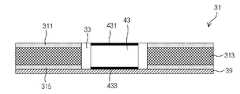
도 2는 상하 방향의 외부 전극을 갖는 전자부품을 내장한 본 발명의 일실시예에 따른 전자부품 내장 인쇄회로기판의 단면도.2 is a cross-sectional view of an electronic component-embedded printed circuit board according to an exemplary embodiment of the present disclosure incorporating an electronic component having external electrodes in a vertical direction.
도 3은 기재가 동박적층판인 본 발명의 다른 실시예에 따른 전자부품 내장 인쇄회로기판의 단면도.3 is a cross-sectional view of an electronic component-embedded printed circuit board according to another embodiment of the present invention, wherein the substrate is a copper clad laminate.
도 4는 전자부품의 일면만 외부 전극을 갖는 본 발명의 또 다른 실시예에 따른 전자부품 내장 인쇄회로기판의 단면도.4 is a cross-sectional view of an electronic component-embedded printed circuit board according to still another embodiment of the present invention in which only one surface of the electronic component has an external electrode.
도 5는 기재가 동박적층판인 본 발명의 또 다른 실시예에 따른 전자부품 내장 인쇄회로기판을 나타낸 단면도.Figure 5 is a cross-sectional view showing a printed circuit board with an electronic component according to another embodiment of the present invention the substrate is a copper clad laminate.
도 6a는 전자부품의 일면에 형성된 외부 전극의 일실시예를 나타내는 개략도.6A is a schematic diagram illustrating an embodiment of an external electrode formed on one surface of an electronic component.
도 6b는 전자부품의 일면에 형성된 외부 전극의 다른 실시예를 나타내는 개략도.6B is a schematic diagram illustrating another embodiment of an external electrode formed on one surface of an electronic component.
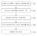
도 7은 본 발명의 일실시예에 따른 전자부품 내장 인쇄회로기판 제조방법을 나타내는 흐름도.7 is a flowchart illustrating a method for manufacturing a printed circuit board with electronic components according to an embodiment of the present invention.
도 8은 기재에 전자부품이 수용되는 삽입공을 형성한 상태를 도시한 단면도.8 is a cross-sectional view showing a state in which an insertion hole in which an electronic component is accommodated is formed in a substrate.
도 9a는 점착시트를 이용하여 전자부품을 고정하는 단계를 나타낸 단면도.9A is a cross-sectional view illustrating a step of fixing an electronic component using an adhesive sheet.
도 9b는 점착제를 도포하여 전자부품을 고정하는 단계를 나타낸 단면도.9B is a cross-sectional view illustrating a step of fixing an electronic component by applying an adhesive.
도 10은 삽입공과 전자부품 사이를 충전한 상태를 나타낸 단면도.10 is a cross-sectional view showing a state where a charge is inserted between an insertion hole and an electronic component.
도 11은 기재의 양면에 전자부품의 전극과 접하는 접합층을 적층한 상태를 나타낸 단면도.11 is a cross-sectional view showing a state in which a bonding layer in contact with an electrode of an electronic component is laminated on both surfaces of a substrate.
도 12는 접합층의 양면에 회로가 형성된 상태를 도시한 단면도.12 is a cross-sectional view showing a state in which circuits are formed on both surfaces of a bonding layer.
*도면의 주요 부분에 대한 도면부호의 설명** Description of reference numerals for the main parts of the drawings *
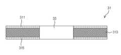
31: 기재 33: 삽입공31: base material 33: insertion hole
35: 충전제 37: 접합층35: Filler 37: Bonding Layer
39: 점착시트 41: 점착제39: adhesive sheet 41: adhesive
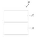
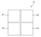
43: 전기부품 431: 제1전극43: electrical component 431: first electrode
433: 제2전극433: second electrode
본 발명은 전자부품을 내장한 인쇄회로기판 및 그 제조방법에 관한 것으로, 더욱 상세하게는 전자부품의 외부 전극에 접하는 접합층을 구비한 전자부품 내장 인쇄회로기판 및 그 제조방법에 관한 것이다.BACKGROUND OF THE INVENTION 1. Field of the Invention The present invention relates to a printed circuit board incorporating an electronic component and a method of manufacturing the same. More particularly, the present invention relates to a printed circuit board incorporating an electronic component and a method of manufacturing the same.
최근 전자기기의 고성능화 및 소형화의 요구에 부응하여 전자부품이 고밀도화 및 고성능화되고 있다. 따라서, 전자부품의 고밀도 실장이 가능한 소형 인쇄회로기판의 수요가 점점 증가하고 있다. 이러한 요구에 부응하여 서로 다른 층에 형성되는 배선 간 또는 전자부품과 배선 간을 비어홀(via hole)에 의하여 전기적으로 접속하는 다층 회로 기판의 개발이 진행되고 있다. 이러한 다층 회로기판은 전자부품 간을 접속하는 배선을 단축할 수 있을 뿐만 아니라 고밀도 배선화를 실현할 수 있는 장점이 있다. 그리고 전자부품의 실장으로 인해 인쇄회로기판의 표면적을 넓힐 뿐만 아니라 전기적 특성도 우수한 장점이 있다.In recent years, in response to the demand for high performance and miniaturization of electronic devices, electronic components have become higher density and higher performance. Accordingly, the demand for small printed circuit boards capable of high density mounting of electronic components is increasing. In response to this demand, development of multilayer circuit boards which electrically connect interconnections formed on different layers or between electronic components and interconnections via via holes has been developed. Such a multilayer circuit board not only shortens the wiring connecting the electronic components, but also has the advantage of realizing high density wiring. In addition, due to the mounting of electronic components, the surface area of the printed circuit board is not only widened, but also has excellent electrical characteristics.
도 1은 종래의 전자부품을 실장한 인쇄회로기판을 나타내는 단면도이다. 종래의 인쇄회로기판(10)은 배선층(11)의 표면에 전자부품(14)을 실장한 후 절연층(12)을 적층하고 그 상면에 다시 배선층(11)을 적층 한다. 그리고 배선층(11)간의 연결 및 배선층(11)과 전자부품(14) 사이의 전기적인 연결을 위하여 다수의 비어홀(via hole, 13)이 형성되어 있다.1 is a cross-sectional view showing a printed circuit board on which a conventional electronic component is mounted. In the conventional
이와 같은 비어홀(13)은, 절연층(12)을 형성하고 홀을 천공한 후 금속을 홀의 내부에 도금함으로써 형성된다. 그러나 이와 같은 비어홀(13)은 그 제작과정이 번거로운 뿐만 아니라, 비어홀(13)에 의해 상기 배선층(11)의 설계에 많은 제약이 따르게 된다.The
또한, 안정적인 인쇄회로기판을 제공하기 위해서는 비어홀(13)의 신뢰성이 중요하다. 그런데 비어홀(13)은 인쇄회로기판의 제작시 발생하는 열 및 사용 환경의 온도 변화에 따른 절연층(12)과의 열팽창의 차이로 인해 비어홀(13)에 응력이 발생하게 되는데, 이와 같은 응력은 비어홀(13)의 접속 신뢰성을 저하하는 원인이 된다.In addition, the reliability of the
본 발명은 상기와 같은 종래기술의 문제점을 해결하기 위해 도출된 것으로,The present invention is derived to solve the problems of the prior art as described above,
본 발명의 목적은 비어홀을 형성할 필요가 없는 전자부품 내장 인쇄회로기판 및 그 제조방법을 제공하는 것이다.An object of the present invention is to provide an electronic component embedded printed circuit board and a method of manufacturing the same, which do not need to form a via hole.
본 발명은 상기와 같은 목적을 달성하기 위하여 다음과 같은 실시예에 의해 구현된다.The present invention is implemented by the following embodiments to achieve the above object.
본 발명의 일실시예에 따른 전자부품 내장 인쇄회로기판은 외부 전극을 구비한 전자부품 내장 인쇄회로기판에 있어서, 전자부품을 수용하는 삽입공이 형성된 기재와, 전자부품과 삽입공 사이에 충전되어 전자부품을 고정하는 충전제와, 기재상에 적층되어 전극과 접하는 접합층을 포함하며, 접합층에는 회로가 형성된다.An electronic component embedded printed circuit board according to an embodiment of the present invention includes a substrate having an insertion hole for accommodating an electronic component, and a charge filled between the electronic component and the insertion hole in an electronic component embedded printed circuit board having an external electrode. And a bonding layer laminated on the substrate and in contact with the electrode, the circuit being formed on the bonding layer.
이와 같은 구성으로 인해 본 발명의 전자부품이 내장된 인쇄회로기판은 접합층과 전자부품의 전극이 직접 접하기 때문에 비어홀을 형성할 필요가 없게 된다. 이로 인해 전자부품의 전기적 접속의 신뢰성을 향상할 수 있고 인쇄회로기판의 설계를 더욱 유연성 있게 할 수 있을 뿐만 아니라 제조 비용 및 시간을 절감할 수 있는 효과를 도모할 수 있다.Due to such a configuration, the printed circuit board in which the electronic component of the present invention is embedded does not need to form a via hole because the bonding layer is directly in contact with the electrode of the electronic component. This can improve the reliability of the electrical connection of electronic components, make the design of the printed circuit board more flexible, and reduce the manufacturing cost and time.
본 발명의 다른 실시예에 따르면, 기재는 전자부품과 실질적으로 동일한 두께를 가지고, 전자부품의 일면에는 제1전극이 타면에는 제2전극이 각각 형성되어 있으며, 접합층은 제1전극과 접하는 제1접합층 및 제2전극과 접하는 제2접합층으로 이루어진다. 본 발명의 또 다른 실시예에 따르면, 전자부품의 일면에는 2 이상의 전극이 형성되어 있으며, 접합층은 전극과 접하는 하나의 접합층을 포함할 수도 있다.According to another embodiment of the present invention, the substrate has a thickness substantially the same as that of the electronic component, the first electrode is formed on one surface of the electronic component, and the second electrode is formed on the other surface, and the bonding layer is formed of the first electrode. A first bonding layer and a second bonding layer in contact with the second electrode. According to another embodiment of the present invention, two or more electrodes are formed on one surface of the electronic component, and the bonding layer may include one bonding layer in contact with the electrode.
기재를 동박적층판으로 형성할 수 있다. 그리고 전자부품은 수동소자뿐만 아니라 능동소자일 수 있으며 수동소자 및 능동소자를 동시에 내장할 수 있다. 또한, 인쇄회로기판은 2 이상의 층으로 적층될 수 있다.A base material can be formed from a copper foil laminated board. In addition, the electronic component may be an active device as well as a passive device, and may simultaneously include a passive device and an active device. Also, the printed circuit board may be stacked in two or more layers.
본 발명의 일실시예에 따른 외부 전극을 구비한 전자부품 내장 인쇄회로기판 제조방법은, 기재에 전자부품이 수용되는 삽입공을 형성하는 단계와, 삽입공에 전자부품을 삽입하여 고정하는 단계와, 삽입공과 전자부품 사이를 충전하는 단계와, 기재의 적어도 일면에 전극과 접하는 접합층을 형성하는 단계와, 접합층에 회로를 형성하는 단계를 포함한다.According to an embodiment of the present invention, there is provided a method of manufacturing an electronic component-embedded printed circuit board having an external electrode, the method including: forming an insertion hole in which an electronic component is accommodated in a substrate; Filling the gap between the insertion hole and the electronic component; forming a bonding layer in contact with the electrode on at least one surface of the substrate; and forming a circuit in the bonding layer.
전자부품을 삽입공 내에 고정하는 단계는 기재의 일면에 점착시트를 부착하여 고정하거나, 점착제를 사용하여 전자부품을 고정할 수 있다. 점착시트 또는 점착제는 열이나 UV광에 의해 점착성을 잃는 물질로 이루질 수 있다.The fixing of the electronic component in the insertion hole may be performed by attaching an adhesive sheet to one surface of the substrate or fixing the electronic component by using an adhesive. The pressure-sensitive adhesive sheet or pressure-sensitive adhesive may be made of a material that loses adhesiveness by heat or UV light.
삽입공을 형성하는 과정에서 발생하는 스미어를 제거하는 디스미어 공정을 추가로 포함하는 것이 바람직하다.It is preferable to further include a desmear process for removing the smear generated in the process of forming the insertion hole.
충전제를 삽입공에 충전하는 단계에서는 진공인쇄기를 이용함으로써 삽입공 내부에 기포의 발생을 차단하는 것이 바람직하다. 기재는 절연층 또는 절연층을 포함하는 동박적층판일 수 있다. 전자부품은 수동소자 및/또는 능동소자일 수 있다.In the filling of the filler into the insertion hole, it is preferable to block the generation of bubbles in the insertion hole by using a vacuum printer. The substrate may be an insulating layer or a copper clad laminate comprising an insulating layer. The electronic component may be a passive element and / or an active element.
삭제delete
도 2는 본 발명의 일실시예에 따른 전자부품 내장 인쇄회로기판의 일실시예에 따른 단면도이다. 도 2에 도시된 바와 같이, 본 발명의 일실시예에 따른 전자부품 내장 인쇄회로기판(30)은 삽입공(33)을 구비하며 전자부품(43)과 실질적으로 동일한 두께를 갖는 기재(31)와, 상기 삽입공(33)에 충전되는 충전제(35)와, 상기 기재(31)의 일면 또는 양면에 적층되는 접합층(37)을 포함한다.2 is a cross-sectional view of an electronic component embedded printed circuit board in accordance with an embodiment of the present invention. As shown in FIG. 2, the electronic component embedded
상기 기재(31)는 상기 접합층(37) 사이에 개재되는 절연층이다. 상기 기재(31)는 열경화성 수지를 포함하는 수지 조성물에 무기 필러(filler)를 분산시킨 층으로 형성될 수 있다. 열경화성 수지로는 에폭시(epoxy) 수지, 페놀(phenol) 수지 또는 이소시아네이트(isocyanate) 수지로부터 선택되는 적어도 한 종류를 포함하는 것이 바람직하다. 이는 열경화성 수지가 기계적 강도 및 내열성이 우수하기 때문이다. 그리고 수지 조성물에는 필요에 따라 커플즈(coupling)제, 분산제 또는 착색제 등의 각종 첨가제를 첨가하여 기재(31)의 성능을 향상시키는 것이 바람직하다. 예를 들면 커플즈제는 수지 조성물과 무기 필러와의 접착성을 개선할 수 있고 분산재는 무기 필러의 분산성을 개선하고 혼합물 내의 얼룩을 제거할 수 있다.The
무기 필러는 Al2O3, MgO, BN, SiO2,SiC, Si3N4등에 의해 구성되는 그룹으로부터 선택된 하나 또는 이들의 조합일 수 있다. 이들 재료는 열전도성이 우수하기 때문에 상기 기재(31)의 방열성을 높일 수 있다.The inorganic filler may be one or a combination thereof selected from the group consisting of Al2 O3 , MgO, BN, SiO2, SiC, Si3 N4, and the like. Since these materials are excellent in thermal conductivity, the heat dissipation of the said
상기 기재(31)의 소정의 위치에는 삽입공(33)이 천공된다. 상기 삽입공(33)에는 상기 전자부품(43)이 삽입되기 때문에, 상기 삽입공(33)의 크기는 상기 전자부품(43)의 크기보다 다소 크게 형성된다. 상기 삽입공(33)을 형성하는 방법으로는 프레싱(pressing), 드릴링(drilling) 또는 레이저 가공 등 다양한 방법이 있다. 드릴링 또는 프레싱 공정을 이용하여 상기 삽입공(33)을 형성하는 경우 발생하는 스미어(smear)를 제거하는 디스미어(desmear) 공정을 추가로 수행하는 것이 바람직하다.The
상기 충전제(35)는 상기 삽입공(33)에 삽입되어 고정된 전자부품(43)과 상기 삽입공(33) 사이에 충전됨으로써 상기 전자부품(43)을 고정하는 역할을 한다. 상기 충전제(35)로는 일반적으로 에폭시 수지를 사용할 수 있다. 상기 충전제(35)를 충전하는 경우, 진공 인쇄기를 사용함으로써 상기 삽입공(33)에서 기포의 발생을 차단하는 것이 바람직하다.The
상기 접합층(37)은 상기 기재(31)의 일면 또는 양면에 적층되는 금속층으로서, 전자부품(43)의 외부 전극(431, 433)과 접한다. 상기 접합층(37)은 구리 도금에 의해 형성될 수 있다. 상기 접합층(37)은 전자부품(43)의 전극(431, 433)과 직접 접하기 때문에, 본 발명의 전자부품 내장 인쇄회로기판은 비어홀을 형성할 필요 가 없게 된다. 따라서 상기 접합층(37) 상에 회로를 형성하는 경우, 종래와 같이 비어홀을 고려할 필요가 없기 때문에, 보다 유연성 있는 설계가 가능하고 제조 비용 및 시간을 절감할 수 있다. 그리고 상기 접합층(37)과 전자부품(43)의 전극(431, 433)이 직접 접하기 때문에 전기적인 신뢰성이 우수하다. 상기 접합층(37)상에는 인쇄회로공정에 의해 각종 회로가 형성된다.The
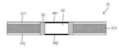
전자부품(43)은 상기 기재(31)와 실질적으로 동일한 두께를 갖는다. 그리고 상면 및 하면에는 제1전극(431) 및 제2전극(433)이 각각 형성되어 있다. 상기 제1전극(431) 및 제2전극(433)은 상기 접합층(37)과 접한다. 전자부품(43)은 트랜지스터(transistor), IC, LSI 등과 같은 능동소자 또는 저항(resistor), 콘덴서(condenser) 또는 인덕터(inductor)와 같은 수동소자일 수 있다.The
도 3은 본 발명의 다른 실시예에 따른 전자부품 내장 인쇄회로기판을 나타낸 단면도이다. 본 실시예에서는 상기 기재(31)를 동박적층판(copper clad laminate, CCL)(31)으로 형성하였다. 상기 동박적층판(31)의 상면 및 하면에 각각 형성된 상부동박(311) 및 하부동박(315) 상에는 접합층(37)이 각각 적층된다. 그리고 상기 상부동박(311) 및 하부동박(315)과 상기 접합층(37)에는 인쇄회로공정에 의해 회로가 형성된다.3 is a cross-sectional view illustrating a printed circuit board having an electronic component according to another embodiment of the present invention. In this embodiment, the
도 4는 본 발명의 다른 실시예에 따른 전자부품 내장 인쇄회로기판의 단면도이다. 전자부품(43)은, 도 5a 내지 도 5b에 도시된 바와 같이 일면에만 외부 전극(431, 433)이 형성되어 있다. 상기 전극(431, 433)은 하나의 접합층(37)과 접한다. 이때, 상기 기재(31)의 두께는 전자부품(43)의 두께와 동일하거나 클 수 있다. 상 기 기재(31)는 도 5에서와 같이 동박적층판(31)으로 형성될 수 있다.4 is a cross-sectional view of an electronic component embedded printed circuit board according to another exemplary embodiment of the present disclosure. As shown in FIGS. 5A to 5B, the
도 6a 내지 도 6b는 전자부품(43)의 외부 전극의 형상을 나타내는 개략도이다. 전자부품(43)의 외부에 형성된 전극은 도 2 내지 도 3에 도시된 바와 같이 상하 방향으로 형성될 수 있지만, 전자부품(43)의 일면에 다수 개가 형성될 수도 있다. 이와 같이 전자부품(43)의 일면에만 전극이 형성된 경우에는 전극과 접하는 접합층(37)을 일면에만 형성할 수 있게 된다.6A to 6B are schematic diagrams showing the shape of the external electrode of the
도 7은 본 발명의 일실시예에 따른 전자부품 내장 인쇄회로기판 제조방법을 나타내는 흐름도이다. 도 7에 도시된 바에 따르면, 본 발명의 일실시예에 따른 전자부품 내장 인쇄회로기판 제조방법은 상기 기재(31)에 전자부품(43)이 수용되는 삽입공(33)을 형성하는 단계(S10), 상기 삽입공(33)에 전자부품(43)을 삽입하여 고정하는 단계(S20), 상기 삽입공(33)과 전자부품(43) 사이를 충전하는 단계(S30), 상기 기재(31)의 일면에 전극과 접하는 상기 접합층(37)을 형성하는 단계(S40) 및 상기 접합층(37)에 회로를 형성하는 단계(S50)를 포함한다. 이하에서는, 상기 S10 단계 내지 S50 단계를 도 8 내지 도 12를 참조하여 설명하기로 한다.7 is a flowchart illustrating a method for manufacturing a printed circuit board with electronic components according to an embodiment of the present invention. As shown in FIG. 7, in the method for manufacturing an electronic component embedded printed circuit board according to an embodiment of the present disclosure, forming an
도 8은 상기 기재(31')에 상기 삽입공(33)을 형성하는 상기 S10 단계에 따른 단면도이다. 상기 삽입공(33)은 프레싱, 드릴링 또는 레이저 가공 등에 의해 형성된다. 상기 삽입공(33)의 크기는 전자부품(43)의 크기보다 다소 크게 형성하여, 상기 삽입공(33)에 전자부품(43)이 수용될 수 있도록 하는 것이 바람직하다.8 is a cross-sectional view taken along the step S10 of forming the
도 9a는 상기 삽입공(33)에 수용된 전자부품(43)을 고정하는 상기 S20 단계의 일실시예를 나타낸 단면도이다. 상기 기재(31)의 일면에는 점착시트(39)가 부착 되는데, 상기 점착시트(39)에 의해 전자부품(43)이 상기 삽입공(33) 내부에서 고정된다. 상기 점착시트(39)는 일반적인 양면 테이프를 사용할 수 있다. 상기 점착시트(39)는 상기 충전제(35)의 충전 후 박리 된다.9A is a cross-sectional view showing an embodiment of the step S20 for fixing the
도 9b는 상기 S10 단계의 다른 실시예를 나타낸 단면도이다. 먼저, 테이블 상(T)에 전자부품(43)의 크기보다 다소 큰 면적으로 점착제(41)를 도포한 후 상기 기재(31) 및 전자부품(43)을 순차적으로 위치시킨다. 상기 점착제(41)는 점착성 잉크를 사용할 수 있다. 전자부품(43)을 점착제(41)에 의해 고정한 상태에서 상기 충전제(35)로 충전한 후, 상기 점착제(41)가 상기 기재(31)의 표면보다 돌출되거나 상기 전자부품(43)의 전극을 덮는 경우는 연마 공정에 의해 이를 제거한다.9B is a sectional view showing another embodiment of the step S10. First, the pressure-
상기 점착시트(39) 또는 상기 점착제(41)는 열이나 UV노광에 의해 점착성을 상실하는 것이 바람직하다. 이로 인해 상기 점착시트(39) 또는 상기 점착제(41)에 의해 전자부품(43)을 고정한 상태에서 충전제를 충전한 후 열이나 UV노광을 가하여 상기 점착시트(39)를 용이하게 분리하거나 상기 기재(31)를 테이블(T)로부터 용이하게 분리할 수 있게 된다.Preferably, the
도 10은 상기 삽입공(33)과 상기 전자부품(43) 사이를 충전하는 상기 S30 단계를 나타낸 단면도이다. 상기 삽입공(33)은 에폭시 수지 등에 의한 충전제(35) 의해 충전됨으로써, 전자부품(43)이 상기 충전제(35)에 의해 고정된다. 상기 충전제(35)는 진공 인쇄기에 의해 충전됨으로써 상기 삽입공(33) 내부의 기포 발생을 억제할 수 있다. 상기 충전제(35)는 일반적으로 플러깅(plugging) 공정에 의해 충전된다.10 is a cross-sectional view showing the step S30 of filling between the
도 11은 상기 기재(31)에 전자부품(43)의 전극(431, 433)과 접하는 상기 접합층(37)을 형성한 상기 S40 단계를 나타낸 단면도이다. 도 11에 도시된 바와 같이 상기 접합층(37)은 구리 도금 등에 의해 상기 기재(31)의 양면에 적층되어 전자부품(43)의 전극(431, 433)과 접합한다. 물론, 도 4 내지 도 5에 도시된 바와 같이 전자부품(43)의 일면에 전극이 형성된 경우에는 상기 접합층(37)을 상기 기재(31)의 일면에만 형성할 수도 있다.11 is a cross-sectional view showing the step S40 in which the
도 12는 상기 접합층(37)에 회로를 형성하는 상기 S50 단계에 따른 단면도이다. 상기 기재(31)의 상부 및 하부에 형성된 접합층(37)에는 일반적인 회로형성공정을 통해 회로가 형성된다. 그리고 전자부품(43)이 내장된 부분에는 상기 접합층(37)을 선택적으로 남겨서 전기적 접속이 가능하게 한다. 이상과 같이 형성된 전자부품 내장 인쇄회로기판(30)을 2층 이상 적층 할 수 있다.12 is a cross-sectional view taken along step S50 of forming a circuit in the
이상과 같은 내용은 본 발명의 기술적 사상을 구현하는 실시예에 불과한 것으로, 본 발명은 상기와 같은 실시예에 한정되지 않고 본 발명의 기술적 사상을 구현하는 한 어떠한 실시예 또는 변경예도 본 발명의 범위에 속하는 것으로 해석되어야 한다.The above description is merely an embodiment for implementing the technical idea of the present invention, the present invention is not limited to the above embodiment and any embodiment or modification as long as the technical idea of the present invention is implemented the scope of the present invention Should be interpreted as belonging to.
본 발명은 상기와 같은 구성에 의해 다음과 같은 효과를 도모할 수 있다.The present invention can achieve the following effects by the above configuration.
본 발명은 전자부품의 전극과 접합층의 직접적인 접합에 의해 전자부품이 연결되기 때문에 전기적인 신뢰성이 우수한 전자부품 내장 인쇄회로기판 및 그 제조방법을 제공할 수 있는 효과를 가진다.The present invention has the effect of providing an electronic component-embedded printed circuit board having excellent electrical reliability and a method of manufacturing the same because the electronic components are connected by direct bonding of the electrode and the bonding layer of the electronic component.
본 발명은 비어홀을 형성할 필요가 없기 때문에 제조가 용이하고 비용 및 시간을 절감할 수 있는 전자부품 내장 인쇄회로기판 및 그 제조방법을 제공할 수 있는 효과를 도모할 수 있다.Since the present invention does not need to form a via hole, the present invention can provide an electronic component-embedded printed circuit board and a method of manufacturing the same, which are easy to manufacture and can reduce cost and time.
Claims (13)
Translated fromKoreanPriority Applications (4)
| Application Number | Priority Date | Filing Date | Title |
|---|---|---|---|
| KR1020050054035AKR100704936B1 (en) | 2005-06-22 | 2005-06-22 | Electronic printed circuit board and its manufacturing method |
| JP2006121165AJP2007005768A (en) | 2005-06-22 | 2006-04-25 | Printed circuit board with built-in electronic component and its manufacturing method |
| CNA200610083575XACN1886026A (en) | 2005-06-22 | 2006-06-07 | Printed circuit board with embedded electronic components |
| US11/452,322US20060291173A1 (en) | 2005-06-22 | 2006-06-14 | Printed circuit board with embedded electronic components |
Applications Claiming Priority (1)
| Application Number | Priority Date | Filing Date | Title |
|---|---|---|---|
| KR1020050054035AKR100704936B1 (en) | 2005-06-22 | 2005-06-22 | Electronic printed circuit board and its manufacturing method |
Publications (2)
| Publication Number | Publication Date |
|---|---|
| KR20060134393A KR20060134393A (en) | 2006-12-28 |
| KR100704936B1true KR100704936B1 (en) | 2007-04-09 |
Family
ID=37567085
Family Applications (1)
| Application Number | Title | Priority Date | Filing Date |
|---|---|---|---|
| KR1020050054035AExpired - Fee RelatedKR100704936B1 (en) | 2005-06-22 | 2005-06-22 | Electronic printed circuit board and its manufacturing method |
Country Status (4)
| Country | Link |
|---|---|
| US (1) | US20060291173A1 (en) |
| JP (1) | JP2007005768A (en) |
| KR (1) | KR100704936B1 (en) |
| CN (1) | CN1886026A (en) |
Cited By (1)
| Publication number | Priority date | Publication date | Assignee | Title |
|---|---|---|---|---|
| KR20210023441A (en)* | 2019-08-23 | 2021-03-04 | 삼성전기주식회사 | Electronic component embedded substrate |
Families Citing this family (34)
| Publication number | Priority date | Publication date | Assignee | Title |
|---|---|---|---|---|
| KR101284042B1 (en)* | 2007-01-25 | 2013-07-09 | 삼성디스플레이 주식회사 | Flexible Printed Circuit Board, Method of Manufacturing The Same and Display Device Having The Same |
| KR100888562B1 (en)* | 2007-02-27 | 2009-03-12 | 대덕전자 주식회사 | Manufacturing method of active circuit embedded printed circuit board |
| KR100832653B1 (en)* | 2007-06-08 | 2008-05-27 | 삼성전기주식회사 | Component embedded printed circuit board and its manufacturing method |
| KR100972431B1 (en)* | 2008-03-25 | 2010-07-26 | 삼성전기주식회사 | Embedded printed circuit board and its manufacturing method |
| KR20090129791A (en) | 2008-06-13 | 2009-12-17 | 가부시키가이샤 교토 소프트웨어 리서치 | Multi-value flash memory |
| TWI373113B (en)* | 2008-07-31 | 2012-09-21 | Unimicron Technology Corp | Method of fabricating printed circuit board having semiconductor components embedded therein |
| US8299366B2 (en)* | 2009-05-29 | 2012-10-30 | Ibiden Co., Ltd. | Wiring board and method for manufacturing the same |
| KR20110002616A (en)* | 2009-07-02 | 2011-01-10 | 삼성에스디아이 주식회사 | Protective Circuit Boards and Secondary Batteries and Battery Packs |
| KR101095130B1 (en)* | 2009-12-01 | 2011-12-16 | 삼성전기주식회사 | Electronic component embedded printed circuit board and manufacturing method |
| EP2372827A1 (en)* | 2010-03-29 | 2011-10-05 | Samsung SDI Co., Ltd. | Sencodary battery pack |
| US20110236727A1 (en)* | 2010-03-29 | 2011-09-29 | Young-Cheol Jang | Secondary battery pack |
| US20110290540A1 (en)* | 2010-05-25 | 2011-12-01 | Samsung Electro-Mechanics Co., Ltd. | Embedded printed circuit board and method of manufacturing the same |
| CN102270622A (en)* | 2010-06-07 | 2011-12-07 | 佳邦科技股份有限公司 | Bare chip size semiconductor element package and manufacturing method thereof |
| KR101752829B1 (en)* | 2010-11-26 | 2017-06-30 | 삼성전자주식회사 | Semiconductor devices |
| AT13055U1 (en)* | 2011-01-26 | 2013-05-15 | Austria Tech & System Tech | METHOD FOR INTEGRATING AN ELECTRONIC COMPONENT INTO A CONDUCTOR PLATE OR A PCB INTERMEDIATE PRODUCT AND PCB OR INTERMEDIATE CIRCUIT PRODUCT |
| CN102300417B (en)* | 2011-08-10 | 2013-09-11 | 深南电路有限公司 | Electronic component embedded type circuit board and manufacture method thereof |
| JP6133549B2 (en)* | 2012-04-26 | 2017-05-24 | 新光電気工業株式会社 | Wiring board and method of manufacturing wiring board |
| KR20150023887A (en)* | 2012-06-29 | 2015-03-05 | 쓰리엠 이노베이티브 프로퍼티즈 컴파니 | A flexible printed circuit and a method of fabricating a flexible printed circuit |
| JP5236826B1 (en)* | 2012-08-15 | 2013-07-17 | 太陽誘電株式会社 | Electronic component built-in board |
| KR102042033B1 (en)* | 2012-10-30 | 2019-11-08 | 엘지이노텍 주식회사 | Printed circuit board for mounting chip and manufacturing method thereof |
| KR101440327B1 (en)* | 2013-02-19 | 2014-09-15 | 주식회사 심텍 | PCB with embedded chip and manufacturing method for the same |
| JP2015050309A (en) | 2013-08-31 | 2015-03-16 | 京セラサーキットソリューションズ株式会社 | Wiring board manufacturing method |
| CN103491719B (en)* | 2013-09-22 | 2017-01-18 | Tcl通讯(宁波)有限公司 | PCB and method for embedding driven elements in PCB |
| US20150279814A1 (en)* | 2014-04-01 | 2015-10-01 | Zhuhai Advanced Chip Carriers & Electronic Substrate Solutions Technologies Co. Ltd. | Embedded chips |
| CN204810668U (en)* | 2014-04-04 | 2015-11-25 | 史利利 | Printed circuit board |
| CN104320925B (en)* | 2014-10-23 | 2018-01-19 | 安捷利(番禺)电子实业有限公司 | A kind of preparation method of new embedded circuit board |
| KR102231101B1 (en)* | 2014-11-18 | 2021-03-23 | 삼성전기주식회사 | Element embedded printed circuit board and method of manufacturing the same |
| CN109561570B (en)* | 2018-11-21 | 2020-12-18 | 奥特斯(中国)有限公司 | Component carrier, method of manufacturing the same, and method of using filler particles |
| CN111354703A (en)* | 2018-12-21 | 2020-06-30 | 深圳市泛宜微电子技术有限公司 | Packaged electronic component and manufacturing method thereof |
| CN111354707A (en)* | 2018-12-21 | 2020-06-30 | 深圳市泛宜微电子技术有限公司 | Packaging module of power device and manufacturing method thereof |
| CN211045436U (en)* | 2019-07-07 | 2020-07-17 | 深南电路股份有限公司 | Circuit board |
| US11497112B2 (en)* | 2020-12-11 | 2022-11-08 | Toyota Motor Engineering & Manufacturing North America, Inc. | Driver board assemblies and methods of forming a driver board assembly |
| US12096561B2 (en) | 2021-11-01 | 2024-09-17 | Raytheon Company | Nanocomposite material for ultraviolet curable direct write semiconductor applications |
| CN115151026B (en)* | 2022-07-30 | 2024-12-17 | 乐健科技(珠海)有限公司 | Preparation method of circuit board embedded with electric insulation radiator |
Citations (4)
| Publication number | Priority date | Publication date | Assignee | Title |
|---|---|---|---|---|
| JPH1041631A (en) | 1996-07-26 | 1998-02-13 | Kokusai Electric Co Ltd | Method for manufacturing high-density mounting substrate with chip embedded structure |
| JP2004335641A (en) | 2003-05-06 | 2004-11-25 | Canon Inc | Manufacturing method of semiconductor device embedded substrate |
| JP2004356588A (en) | 2003-05-30 | 2004-12-16 | Toppan Printing Co Ltd | Material processing method using ultrashort pulse laser, printed wiring board, and manufacturing method thereof |
| JP2005142178A (en) | 2003-11-04 | 2005-06-02 | Cmk Corp | Multi-layer printed wiring board with built-in electronic components |
Family Cites Families (1)
| Publication number | Priority date | Publication date | Assignee | Title |
|---|---|---|---|---|
| JP3926141B2 (en)* | 2000-12-27 | 2007-06-06 | 日本特殊陶業株式会社 | Wiring board |
- 2005
- 2005-06-22KRKR1020050054035Apatent/KR100704936B1/ennot_activeExpired - Fee Related
- 2006
- 2006-04-25JPJP2006121165Apatent/JP2007005768A/enactivePending
- 2006-06-07CNCNA200610083575XApatent/CN1886026A/enactivePending
- 2006-06-14USUS11/452,322patent/US20060291173A1/ennot_activeAbandoned
Patent Citations (4)
| Publication number | Priority date | Publication date | Assignee | Title |
|---|---|---|---|---|
| JPH1041631A (en) | 1996-07-26 | 1998-02-13 | Kokusai Electric Co Ltd | Method for manufacturing high-density mounting substrate with chip embedded structure |
| JP2004335641A (en) | 2003-05-06 | 2004-11-25 | Canon Inc | Manufacturing method of semiconductor device embedded substrate |
| JP2004356588A (en) | 2003-05-30 | 2004-12-16 | Toppan Printing Co Ltd | Material processing method using ultrashort pulse laser, printed wiring board, and manufacturing method thereof |
| JP2005142178A (en) | 2003-11-04 | 2005-06-02 | Cmk Corp | Multi-layer printed wiring board with built-in electronic components |
Cited By (2)
| Publication number | Priority date | Publication date | Assignee | Title |
|---|---|---|---|---|
| KR20210023441A (en)* | 2019-08-23 | 2021-03-04 | 삼성전기주식회사 | Electronic component embedded substrate |
| KR102703776B1 (en)* | 2019-08-23 | 2024-09-04 | 삼성전기주식회사 | Electronic component embedded substrate |
Also Published As
| Publication number | Publication date |
|---|---|
| CN1886026A (en) | 2006-12-27 |
| US20060291173A1 (en) | 2006-12-28 |
| KR20060134393A (en) | 2006-12-28 |
| JP2007005768A (en) | 2007-01-11 |
Similar Documents
| Publication | Publication Date | Title |
|---|---|---|
| KR100704936B1 (en) | Electronic printed circuit board and its manufacturing method | |
| KR100788213B1 (en) | Manufacturing Method of Electronic Circuit Board | |
| KR101601815B1 (en) | Embedded board, printed circuit board and method of manufactruing the same | |
| KR20090130727A (en) | Electronic component embedded printed circuit board and manufacturing method | |
| KR100999531B1 (en) | Printed circuit board and manufacturing method thereof | |
| KR20080076241A (en) | Electronic circuit board and manufacturing method | |
| TW201306687A (en) | Method for manufacturing printed circuit board | |
| JP2001274556A (en) | Printed wiring board | |
| KR100747022B1 (en) | Embedded printed circuit board and its manufacturing method | |
| KR101044105B1 (en) | Substrate manufacturing method for preventing warpage | |
| CN104247582B (en) | Printed circuit board and manufacturing method thereof | |
| JP2019067858A (en) | Printed wiring board and manufacturing method thereof | |
| KR100972431B1 (en) | Embedded printed circuit board and its manufacturing method | |
| KR100905642B1 (en) | Chip embedded printed circuit board and its manufacturing method | |
| JP2008016805A (en) | Printed circuit board, and method of manufacturing the same | |
| KR100648971B1 (en) | Manufacturing method of embedded printed circuit board | |
| KR100771320B1 (en) | Chip embedded printed circuit board and its manufacturing method | |
| KR100650707B1 (en) | Embedded printed circuit board and its manufacturing method | |
| JP2006049762A (en) | Part built-in substrate and manufacturing method thereof | |
| KR100966341B1 (en) | Printed circuit board and manufacturing method thereof | |
| JP2011222962A (en) | Print circuit board and method of manufacturing the same | |
| KR100771319B1 (en) | Chip embedded printed circuit board and its manufacturing method | |
| KR101084776B1 (en) | Electronic device embedded board and manufacturing method | |
| KR100594454B1 (en) | Printed Circuit Board Device for Mobile Terminal | |
| KR20100053761A (en) | Embedded pcb using unclad and embedded pcb manufactured thereby |
Legal Events
| Date | Code | Title | Description |
|---|---|---|---|
| A201 | Request for examination | ||
| PA0109 | Patent application | St.27 status event code:A-0-1-A10-A12-nap-PA0109 | |
| PA0201 | Request for examination | St.27 status event code:A-1-2-D10-D11-exm-PA0201 | |
| E902 | Notification of reason for refusal | ||
| PE0902 | Notice of grounds for rejection | St.27 status event code:A-1-2-D10-D21-exm-PE0902 | |
| P11-X000 | Amendment of application requested | St.27 status event code:A-2-2-P10-P11-nap-X000 | |
| P13-X000 | Application amended | St.27 status event code:A-2-2-P10-P13-nap-X000 | |
| PG1501 | Laying open of application | St.27 status event code:A-1-1-Q10-Q12-nap-PG1501 | |
| E701 | Decision to grant or registration of patent right | ||
| PE0701 | Decision of registration | St.27 status event code:A-1-2-D10-D22-exm-PE0701 | |
| GRNT | Written decision to grant | ||
| PR0701 | Registration of establishment | St.27 status event code:A-2-4-F10-F11-exm-PR0701 | |
| PR1002 | Payment of registration fee | St.27 status event code:A-2-2-U10-U11-oth-PR1002 Fee payment year number:1 | |
| PG1601 | Publication of registration | St.27 status event code:A-4-4-Q10-Q13-nap-PG1601 | |
| R18-X000 | Changes to party contact information recorded | St.27 status event code:A-5-5-R10-R18-oth-X000 | |
| FPAY | Annual fee payment | Payment date:20100330 Year of fee payment:4 | |
| PR1001 | Payment of annual fee | St.27 status event code:A-4-4-U10-U11-oth-PR1001 Fee payment year number:4 | |
| LAPS | Lapse due to unpaid annual fee | ||
| PC1903 | Unpaid annual fee | St.27 status event code:A-4-4-U10-U13-oth-PC1903 Not in force date:20110403 Payment event data comment text:Termination Category : DEFAULT_OF_REGISTRATION_FEE | |
| PC1903 | Unpaid annual fee | St.27 status event code:N-4-6-H10-H13-oth-PC1903 Ip right cessation event data comment text:Termination Category : DEFAULT_OF_REGISTRATION_FEE Not in force date:20110403 | |
| R18-X000 | Changes to party contact information recorded | St.27 status event code:A-5-5-R10-R18-oth-X000 | |
| R18-X000 | Changes to party contact information recorded | St.27 status event code:A-5-5-R10-R18-oth-X000 |