KR100704470B1 - Method for manufacturing semiconductor device using amorphous carbon film as sacrificial hard mask - Google Patents
Method for manufacturing semiconductor device using amorphous carbon film as sacrificial hard maskDownload PDFInfo
- Publication number
- KR100704470B1 KR100704470B1KR1020040059535AKR20040059535AKR100704470B1KR 100704470 B1KR100704470 B1KR 100704470B1KR 1020040059535 AKR1020040059535 AKR 1020040059535AKR 20040059535 AKR20040059535 AKR 20040059535AKR 100704470 B1KR100704470 B1KR 100704470B1
- Authority
- KR
- South Korea
- Prior art keywords
- film
- hard mask
- sacrificial hard
- etching
- pattern
- Prior art date
- Legal status (The legal status is an assumption and is not a legal conclusion. Google has not performed a legal analysis and makes no representation as to the accuracy of the status listed.)
- Expired - Fee Related
Links
Images


Classifications
- H—ELECTRICITY
- H01—ELECTRIC ELEMENTS
- H01L—SEMICONDUCTOR DEVICES NOT COVERED BY CLASS H10
- H01L21/00—Processes or apparatus adapted for the manufacture or treatment of semiconductor or solid state devices or of parts thereof
- H01L21/02—Manufacture or treatment of semiconductor devices or of parts thereof
- H01L21/04—Manufacture or treatment of semiconductor devices or of parts thereof the devices having potential barriers, e.g. a PN junction, depletion layer or carrier concentration layer
- H01L21/18—Manufacture or treatment of semiconductor devices or of parts thereof the devices having potential barriers, e.g. a PN junction, depletion layer or carrier concentration layer the devices having semiconductor bodies comprising elements of Group IV of the Periodic Table or AIIIBV compounds with or without impurities, e.g. doping materials
- H01L21/30—Treatment of semiconductor bodies using processes or apparatus not provided for in groups H01L21/20 - H01L21/26
- H01L21/302—Treatment of semiconductor bodies using processes or apparatus not provided for in groups H01L21/20 - H01L21/26 to change their surface-physical characteristics or shape, e.g. etching, polishing, cutting
- H01L21/306—Chemical or electrical treatment, e.g. electrolytic etching
- H—ELECTRICITY
- H01—ELECTRIC ELEMENTS
- H01L—SEMICONDUCTOR DEVICES NOT COVERED BY CLASS H10
- H01L21/00—Processes or apparatus adapted for the manufacture or treatment of semiconductor or solid state devices or of parts thereof
- H01L21/02—Manufacture or treatment of semiconductor devices or of parts thereof
- H01L21/027—Making masks on semiconductor bodies for further photolithographic processing not provided for in group H01L21/18 or H01L21/34
- H01L21/033—Making masks on semiconductor bodies for further photolithographic processing not provided for in group H01L21/18 or H01L21/34 comprising inorganic layers
- H01L21/0332—Making masks on semiconductor bodies for further photolithographic processing not provided for in group H01L21/18 or H01L21/34 comprising inorganic layers characterised by their composition, e.g. multilayer masks, materials
- H—ELECTRICITY
- H01—ELECTRIC ELEMENTS
- H01L—SEMICONDUCTOR DEVICES NOT COVERED BY CLASS H10
- H01L21/00—Processes or apparatus adapted for the manufacture or treatment of semiconductor or solid state devices or of parts thereof
- H01L21/02—Manufacture or treatment of semiconductor devices or of parts thereof
- H01L21/02104—Forming layers
- H01L21/02107—Forming insulating materials on a substrate
- H01L21/02109—Forming insulating materials on a substrate characterised by the type of layer, e.g. type of material, porous/non-porous, pre-cursors, mixtures or laminates
- H01L21/02112—Forming insulating materials on a substrate characterised by the type of layer, e.g. type of material, porous/non-porous, pre-cursors, mixtures or laminates characterised by the material of the layer
- H01L21/02115—Forming insulating materials on a substrate characterised by the type of layer, e.g. type of material, porous/non-porous, pre-cursors, mixtures or laminates characterised by the material of the layer the material being carbon, e.g. alpha-C, diamond or hydrogen doped carbon
- H—ELECTRICITY
- H01—ELECTRIC ELEMENTS
- H01L—SEMICONDUCTOR DEVICES NOT COVERED BY CLASS H10
- H01L21/00—Processes or apparatus adapted for the manufacture or treatment of semiconductor or solid state devices or of parts thereof
- H01L21/02—Manufacture or treatment of semiconductor devices or of parts thereof
- H01L21/04—Manufacture or treatment of semiconductor devices or of parts thereof the devices having potential barriers, e.g. a PN junction, depletion layer or carrier concentration layer
- H01L21/18—Manufacture or treatment of semiconductor devices or of parts thereof the devices having potential barriers, e.g. a PN junction, depletion layer or carrier concentration layer the devices having semiconductor bodies comprising elements of Group IV of the Periodic Table or AIIIBV compounds with or without impurities, e.g. doping materials
- H01L21/30—Treatment of semiconductor bodies using processes or apparatus not provided for in groups H01L21/20 - H01L21/26
- H01L21/31—Treatment of semiconductor bodies using processes or apparatus not provided for in groups H01L21/20 - H01L21/26 to form insulating layers thereon, e.g. for masking or by using photolithographic techniques; After treatment of these layers; Selection of materials for these layers
- H01L21/3205—Deposition of non-insulating-, e.g. conductive- or resistive-, layers on insulating layers; After-treatment of these layers
- H01L21/321—After treatment
- H01L21/3213—Physical or chemical etching of the layers, e.g. to produce a patterned layer from a pre-deposited extensive layer
- H01L21/32139—Physical or chemical etching of the layers, e.g. to produce a patterned layer from a pre-deposited extensive layer using masks
Landscapes
- Engineering & Computer Science (AREA)
- Physics & Mathematics (AREA)
- Condensed Matter Physics & Semiconductors (AREA)
- General Physics & Mathematics (AREA)
- Manufacturing & Machinery (AREA)
- Computer Hardware Design (AREA)
- Microelectronics & Electronic Packaging (AREA)
- Power Engineering (AREA)
- Chemical & Material Sciences (AREA)
- Inorganic Chemistry (AREA)
- Internal Circuitry In Semiconductor Integrated Circuit Devices (AREA)
- Drying Of Semiconductors (AREA)
- Semiconductor Memories (AREA)
- Photosensitive Polymer And Photoresist Processing (AREA)
- Materials For Photolithography (AREA)
- Exposure Of Semiconductors, Excluding Electron Or Ion Beam Exposure (AREA)
Abstract
Translated fromKoreanDescription
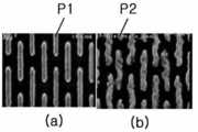
Translated fromKorean도 1은 ArF 포토리소그라피 공정을 적용한 마스크 패턴과 KrF 포토리소그라피 공정을 적용한 라인 타입의 마스크 패턴을 비교 도시한 평면 사진.1 is a planar photograph illustrating a comparison between a mask pattern to which an ArF photolithography process is applied and a mask pattern of a line type to which KrF photolithography process is applied.
도 2는 도 1의 마스크 패턴을 이용하여 식각 공정을 진행한 후의 평면 사진.FIG. 2 is a planar photograph after an etching process is performed using the mask pattern of FIG. 1. FIG.
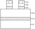
도 3a 내지 도 3d는 종래기술에 따른 F2 또는 ArF 노광원을 이용한 반도체소자 패턴 형성 공정을 도시한 단면도.3A to 3D are cross-sectional views showing a semiconductor device pattern forming process using an F2 or ArF exposure source according to the prior art.
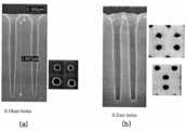
도 4는 비결정성 탄소막을 하드마스크로 사용하여 콘택홀을 형성한 예를 도시한 단면 사진.4 is a cross-sectional view showing an example in which a contact hole is formed using an amorphous carbon film as a hard mask.
도 5는 포토레지스트 패턴을 식각마스크로 사용하는 경우와 비결정성 탄소막을 희생하드마스크로 사용하는 경우의 콘택홀 패턴을 비교 도시한 사진.FIG. 5 is a photograph showing a comparison between contact hole patterns when using a photoresist pattern as an etching mask and when using an amorphous carbon film as a sacrificial hard mask. FIG.
도 6a 내지 도 6f는 본 발명의 제1실시예에 따른 F2 또는 ArF 노광원을 이용한 반도체소자 패턴 형성 공정을 도시한 단면도.6A to 6F are cross-sectional views illustrating a semiconductor device pattern forming process using an F2 or ArF exposure source according to a first embodiment of the present invention.
도 7은 본 발명의 제2실시예에 따른 비결정성 탄소막을 희생 하드마스크로 사용하는 도전패턴 형성을 위한 적층 구조를 도시한 단면도.7 is a cross-sectional view illustrating a laminated structure for forming a conductive pattern using an amorphous carbon film as a sacrificial hard mask according to a second embodiment of the present invention.
도 8은 본 발명의 제3실시예에 따른 비결정성 탄소막을 희생 하드마스크로 사용하는 도전패턴 형성을 위한 적층 구조를 도시한 단면도.FIG. 8 is a cross-sectional view illustrating a laminated structure for forming a conductive pattern using an amorphous carbon film as a sacrificial hard mask according to a third embodiment of the present invention. FIG.
도 9는 본 발명의 제4실시예에 따른 비결정성 탄소막을 희생 하드마스크로 사용하는 도전패턴 형성을 위한 적층 구조를 도시한 단면도.9 is a cross-sectional view illustrating a laminated structure for forming a conductive pattern using an amorphous carbon film as a sacrificial hard mask according to a fourth embodiment of the present invention.
도 10a 내지 도 10d는 본 발명의 제5실시예에 따른 F2 또는 ArF 노광원을 이용한 반도체소자의 패턴 형성 공정을 도시한 단면도.10A to 10D are cross-sectional views illustrating a pattern forming process of a semiconductor device using an F2 or ArF exposure source according to a fifth embodiment of the present invention.
도 11은 본 발명의 제6실시예에 따른 비결정성 탄소막을 희생 하드마스크로 사용하는 콘택홀 형성을 위한 적층 구조를 도시한 단면도.FIG. 11 is a cross-sectional view illustrating a laminated structure for forming a contact hole using an amorphous carbon film as a sacrificial hard mask according to a sixth embodiment of the present invention; FIG.
도 12은 본 발명의 제7실시예에 따른 비결정성 탄소막을 희생 하드마스크로 사용하는 콘택홀 형성을 위한 적층 구조를 도시한 단면도.12 is a cross-sectional view illustrating a laminated structure for forming a contact hole using an amorphous carbon film as a sacrificial hard mask according to a seventh embodiment of the present invention.
도 13는 본 발명의 제8실시예에 따른 비결정성 탄소막을 희생 하드마스크로 사용하는 콘택홀 형성을 위한 적층 구조를 도시한 단면도.FIG. 13 is a cross-sectional view illustrating a laminated structure for forming a contact hole using an amorphous carbon film as a sacrificial hard mask according to an eighth embodiment of the present invention; FIG.
도 14는 금속배선 형성을 위한 마스크 패턴이 형성된 반도체소자를 도시한 평면도.14 is a plan view illustrating a semiconductor device on which a mask pattern for forming metal wirings is formed.
도 15는 도 14를 a-a' 방향으로 절취한 단면도.15 is a cross-sectional view taken along the line a-a 'of FIG. 14;
도 16은 스토리지노드 콘택 형성을 위한 마스크 패턴이 형성된 반도체소자를 도시한 평면도.16 is a plan view illustrating a semiconductor device in which a mask pattern for forming a storage node contact is formed.
도 17은 도 16을 b-b' 방향으로 절취한 단면도.17 is a cross-sectional view taken along the line b-b 'of FIG. 16;
도 18은 ArF 포토리소그라피 공정을 적용한 콘택홀 형성 후의 종래기술과 본발명의 차이점을 비교 도시한 평면 사진.
FIG. 18 is a planar photograph illustrating the difference between the prior art and the present invention after contact hole formation to which an ArF photolithography process is applied. FIG.
* 도면의 주요 부분에 대한 부호의 설명* Explanation of symbols for the main parts of the drawings
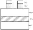
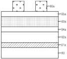
60 : 기판61a : 전도층60
62a : 하드마스크용 절연막63a : 희생 하드마스크용 비결정성 탄소막62a: insulating film for
65a : 반사방지막64a : 희생 하드마스크용 물질막65a:
66a : 포토레지스트 패턴
66a: photoresist pattern
본 발명은 반도체소자 제조 방법에 관한 것으로, 특히 반도체소자의 패턴 형성방법에 관한 것으로, 더욱 상세하게는 F2 또는 불화아르곤(ArF)등의 보다 발전된(Advanced) 노광원을 이용한 반도체소자의 패턴 형성방법에 관한 것이다.BACKGROUND OF THE
반도체소자의 진전을 지지해 온 미세 가공 기술은 사진식각(Photo lithography) 기술인 바, 이 기술의 해상력 향상이 반도체소자의 고집적화의 장래와 직결된다고 해도 과언은 아니다.Since the microfabrication technology that has supported the progress of semiconductor devices is a photolithography technology, it is no exaggeration to say that the improvement in resolution of the technology is directly connected to the future of high integration of semiconductor devices.
이러한 사진식각 공정은 주지된 바와 같이, 포토레지스트 패턴을 형성하는 공정과 상기 포토레지스트 패턴을 식각 마스크로 하는 식각 공정을 통해 피식각층을 식각해서 원하는 형태의 패턴 예컨대, 콘택홀 또는 게이트전극 등의 라인 패턴 등을 형성하는 공정을 포함하는 바, 여기서 포토레지스트 패턴은 피식각층 상에 포토레지스트를 도포하는 공정과 준비된 노광 마스크를 이용해 포토레지스트를 선택적으로 노광하는 공정 및 소정의 화학용액으로 노광되거나, 또는 노광되지 않은 포토레지스트 부분을 제거하는 현상 공정을 통해 이루어진다.The photolithography process is, as is well known, by etching a layer to be etched through a process of forming a photoresist pattern and an etching process using the photoresist pattern as an etch mask, for example, a line of a pattern such as a contact hole or a gate electrode. A process of forming a pattern or the like, wherein the photoresist pattern is a process of applying the photoresist on the etched layer, a process of selectively exposing the photoresist using a prepared exposure mask and a predetermined chemical solution, or Through a developing process to remove unexposed portions of the photoresist.
한편, 사진식각 공정으로 구현할 수 있는 패턴의 임계치수(Critical Dimension; 이하 CD라 함)는 상기한 노광 공정에서 어떤 파장의 광원을 사용하느냐에 따라 좌우된다. 이것은 노광 공정을 통해 구현할 수 있는 포토레지스트 패턴의 폭에 따라 실제 패턴의 CD가 결정되기 때문이다.On the other hand, the critical dimension of the pattern that can be implemented by the photolithography process (hereinafter referred to as CD) depends on the wavelength of the light source used in the above exposure process. This is because the CD of the actual pattern is determined by the width of the photoresist pattern that can be realized through the exposure process.
636㎚ (g-line)의 파장의 광원과 365㎚(i-line)의 광원을 사용하던 초기의 스테퍼(Stepper)를 거쳐 현재는 248㎚(KrF Excimer Laser) 파장의 DUV(Deep Ultra-violet)를 이용하는 스테퍼나 스캐너 타입의 노광장비를 주로 사용하고 있는 바, 248㎚의 DUV 사진식각 기술은 초기에 시간 지연 효과, 기질 의존성 등과 같은 많은 문제들이 발생하였으며, 0.18㎛ 디자인의 제품 개발에 사용되었다. 그러나 0.15㎛ 이하의 디자인을 갖는 제품을 개발하기 위해서는 새로운 193㎚(ArF Excimer Laser) 또는 157nm(F2 Laser)의 파장을 갖는 새로운 DUV 사진식각 기술로의 기술개발이 필수적이다. 그러나, 이러한 DUV 사진식각 기술에서 해상력을 높이기 위한 여러 기술을 조합한다 하여도 0.1㎛ 이하의 패턴은 불가능하므로 새로운 광원을 갖는 사진식 각 기술의 개발이 활발히 진행되고 있다.Deep Ultra-violet (DUV) at 248nm (KrF Excimer Laser) through the early stepper that used 636nm (g-line) light source and 365nm (i-line) light source The 248nm DUV photolithography technology has been used for the development of products with 0.18µm design. However, in order to develop a product with a design of 0.15 μm or less, it is necessary to develop a new DUV photolithography technique having a wavelength of 193 nm (ArF Excimer Laser) or 157 nm (F2 Laser). However, even if a combination of various techniques for enhancing the resolution in the DUV photolithography technique is impossible to pattern less than 0.1㎛, the development of a photolithographic technique having a new light source is actively progressing.
ArF 노광원을 이용한 포토리소그라피 공정과 F2 노광원을 이용하는 포토리소그라피 공정 기술의 핵심 과제 중의 하나는 F2 또는 ArF용 포토레지스트의 개발이다. F2 또는 ArF는 KrF와 같은 화학 증폭형이지만 재료를 근본적으로 개량해야 하는 필요가 있기 때문인데, 특히 ArF 포토레지스트 재료 개발이 어려운 것은 벤젠고리를 사용할 수 없기 때문이다. 벤젠고리는 건식 식각(Dry etching) 내성을 확보하기 위해 i-선 및 KrF용 포토레지스트에 사용되어 왔다. 그러나 예컨대, ArF용 포토레지스트에 벤젠고리가 사용될 경우 ArF 레이저의 파장영역인 193nm에서 흡광도가 크기 때문에 투명성이 떨어져 포토레지스트 하부까지 노광이 불가능한 문제가 발생한다. 이 때문에, 벤젠고리를 가지지 않고 건식 식각 내성을 확보할 수 있으며, 접착력이 좋고 2.38% TMAH(Tetra Methyl Ammonium Hydroxide)로 현상되어질 수 있는 재료의 연구가 진행 되고 있다. 현재까지 세계적으로 많은 회사 및 연구소에서 연구성과를 발표하고 있는 상태이며, 아직까지 상용화 되어 있는 것으로는 COMA(CycloOlefin-Maleic Anhydride) 또는 아크릴레이드(Acrylate) 계통의 폴리머 형태, 또는 이들의 혼합 형태이다. 하지만, 상기한 포토레지스트는 벤젠 구조를 가지고 있다.One of the key challenges of the photolithography process using an ArF exposure source and the photolithography process technology using an F2 exposure source is the development of a photoresist for F2 or ArF. Although F2 or ArF is a chemically amplified type such as KrF, it is necessary to fundamentally improve the material. Particularly, development of ArF photoresist material is difficult because benzene rings cannot be used. Benzene rings have been used in photoresists for i-rays and KrF to ensure dry etching resistance. However, for example, when the benzene ring is used in the ArF photoresist, since the absorbance is large at 193 nm, which is the wavelength region of the ArF laser, the transparency is poor and the exposure to the lower portion of the photoresist is impossible. For this reason, research has been conducted on materials that can secure dry etching resistance without having a benzene ring, have good adhesion, and can be developed with 2.38% TMAH (Tetra Methyl Ammonium Hydroxide). To date, many companies and research institutes around the world have been publishing their research results, and the commercialized products are still in the form of polymers of COMA (CycloOlefin-Maleic Anhydride) or Acrylate series, or a mixture thereof. However, the photoresist has a benzene structure.
도 1은 ArF 포토리소그라피 공정을 적용한 마스크 패턴과 KrF 포토리소그라피 공정을 적용한 라인 타입의 마스크 패턴을 비교 도시한 평면 사진이며, 도 2는 도 1의 마스크 패턴을 이용하여 식각 공정을 진행한 후의 평면 사진이다.FIG. 1 is a planar photograph illustrating a comparison between a mask pattern to which an ArF photolithography process is applied and a mask pattern of a line type to which KrF photolithography process is applied, and FIG. 2 is a planar photograph after an etching process using the mask pattern of FIG. 1. to be.
도 1의 (a)에 도시된 바와 같이, KrF 포토리소그라피 공정을 적용할 경우 마스크 패턴(M1)의 변형이 거의 발생하지 않은 반면, ArF 포토리소그라피 공정을 적용할 경우에는 스트라이에이션(Striation)과 같은 마스크 패턴(M2)의 변형이 일어남을 확인할 수 있다.As shown in (a) of FIG. 1, when the KrF photolithography process is applied, deformation of the mask pattern M1 hardly occurs, whereas when the ArF photolithography process is applied, such as striation. It can be seen that deformation of the mask pattern M2 occurs.
도 2의 (a)와 같이 KrF 포토리소그라피 공정을 적용할 경우에는 패턴(P1)의 변형이 거의 발생하지 않고 마스크 패턴(M1)의 형상이 그대로 전사되는 반면, ArF 포토리소그라피 공정을 적용할 경우에는 패턴(P2)을 형성하기 위해 식각공정을 진행할 때 포토레지스트가 뭉치거나(Cluster) 성형 변형(Plastic deformation)되는 현상과 식각 도중 포토레지스트의 내성이 약하여 한쪽으로 몰리는 현상으로 패턴(P2)에 심한 변형이 발생함을 확인할 수 있다.When the KrF photolithography process is applied as shown in FIG. 2A, the deformation of the pattern P1 hardly occurs and the shape of the mask pattern M1 is transferred as it is, whereas when the ArF photolithography process is applied. When the etching process is performed to form the pattern P2, the photoresist aggregates or forms plastic deformation and the photoresist is weakly crushed to one side due to the weak resistance of the photoresist during etching. It can be confirmed that this occurs.
ArF 포토리소그라피 공정을 이용한 패턴 형성시 상술한 바와 같은 패턴 변형을 최소화하기 위해 텅스텐과 질화막의 단독 또는 적층된 구조의 희생 하드마스크를 사용하는 공정 기술이 개발되었다.In order to minimize the pattern deformation as described above in the pattern formation using the ArF photolithography process, a process technology using a sacrificial hard mask of a single layer or a laminated structure of tungsten and nitride film has been developed.
도 3a 내지 도 3d는 종래기술에 따른 F2 또는 ArF 노광원을 이용한 반도체소자 패턴 형성 공정을 도시한 단면도로서, 이를 참조하여 상세히 설명한다.3A to 3D are cross-sectional views illustrating a semiconductor device pattern forming process using an F2 or ArF exposure source according to the prior art, which will be described in detail with reference to the drawings.
후술하는 반도체소자의 라인 패턴은 구체적으로, 도전패턴 중 비트라인 형성 공정을 그 일예로 한다.Specifically, the line pattern of the semiconductor device, which will be described later, uses a bit line forming process among conductive patterns as an example.
먼저, 도 3a에 도시된 바와 같이, 반도체소자를 형성하기 위한 여러 요소가 형성된 기판(30) 상에 피식각층으로 전도층(31a)을 형성한 다음, 전도층(31a) 상에 절연성 물질이면서도 피식각층인 전도층(31a)과 선택비를 가져 하드마스크 재료로 사용되는 Si3N4 또는 SiON 등의 질화막 계열의 박막 또는 SiO2 등의 산화막 계열의 박막을 사용하여 하드마스크용 절연막(32a)을 증착한다. 이어서, 식각공정시 하드마스크용 절연막(32a)의 손실에 따른 패턴 변형을 방지하기 위해 하드마스크용 절연막(32a) 상에 하드마스크용 희생막(33a)을 형성한다.First, as shown in FIG. 3A, a
여기서, 하드마스크용 희생막(33a)은 폴리실리콘막, Al막, W막, WSix(x는 1 내지 2)막, WN막, Ti막, TiN막, TiSix(x는 1 내지 2)막, TiAlN막, TiSiN막, Pt막, Ir막, IrO2막, Ru막, RuO2막, Ag막, Au막, Co막, Au막, TaN막, CrN막, CoN막, MoN막, MoSix(x는 1 내지 2)막, Al2O3막, AlN막, PtSix(x는 1 내지 2)막 및 CrSix(x는 1 내지 2)막으로 이루어진 그룹으로부터 선택된 적어도 어느 하나의 박막을 이용한다.Here, the hard mask sacrificial film 33a includes a polysilicon film, an Al film, a W film, a WSix (x is 1 to 2) film, a WN film, a Ti film, a TiN film, a TiSix (x is 1 to 2) film, TiAlN film, TiSiN film, Pt film, Ir film, IrO2 film, Ru film, RuO2 film, Ag film, Au film, Co film, Au film, TaN film, CrN film, CoN film, MoN film, MoSix (x At least one thin film selected from the group consisting of 1 to 2) film, Al2 O3 film, AlN film, PtSix (x is 1 to 2) film and CrSix (x is 1 to 2) film.
이어서, 하드마스크용 희생막(33a) 상에 패턴 형성을 위한 노광시 하부 즉, 하드마스크용 희생막(33a)의 광반사도가 높음으로 인해 난반사가 이루어져 원하지 않는 패턴이 형성되는 것을 방지하며, 하드마스크용 희생막(33a)과 후속 포토레지스트의 접착력을 향상시킬 목적으로 반사방지막(34a, ARC)을 형성한다.Subsequently, due to the high light reflectance of the lower portion of the hard mask sacrificial layer 33a, that is, the hard mask sacrificial layer 33a, the diffuse reflection is prevented from forming an unwanted pattern. The antireflection films 34a and ARC are formed to improve the adhesion between the sacrificial film 33a for the mask and the subsequent photoresist.
여기서, 반사방지막(34a)은 포토레지스트와 그 식각 특성이 유사한 유기계열(Organic)의 물질을 주로 이용한다.Here, the anti-reflection film 34a mainly uses an organic material similar to the photoresist and its etching characteristics.
이어서, 반사방지막(34a) 상에 F2 노광원용 또는 ArF 노광원용의 포토레지스 트 스핀 코팅(Spin coating) 등의 방법을 통해 적절한 두께로 도포한 다음, F2 노광원 또는 ArF 노광원과 게이트전극 폭을 정의하기 위한 소정의 레티클(도시하지 않음)을 이용하여 포토레지스트의 소정 부분을 선택적으로 노광하고, 현상 공정을 통해 노광 공정에 의해 노광되거나 혹은 노광되지 않은 부분을 잔류시킨 다음, 후세정 공정 등을 통해 식각 잔유물 등을 제거함으로써 포토레지스트 패턴(35a)을 형성한다.Then, one on top of the anti-reflective film (34a) through a F2 exposure distance or ArF method such as photoresist agent spin coating of the exposure distance (Spin coating) applied at a suitable thickness, and then, F2 exposure light source or the ArF exposure light source and a gate electrode A predetermined portion of the photoresist is selectively exposed using a predetermined reticle (not shown) to define the width, the exposed or unexposed portion of the photoresist is left through a developing process, and then the post-cleaning process The
이어서, 도 3b에 도시된 바와 같이, 포토레지스트 패턴(35b)을 식각마스크로 하는 선택적 식각 공정을 통해 반사방지막(34b)을 선택적으로 식각한다.3B, the
이어서, 포토레지스트 패턴(35b)을 식각마스크로 하드마스크용 희생막(33a)을 식각하여 희생 하드마스크(33b)를 형성한다.Next, the sacrificial
이어서, 도 3c에 도시된 바와 같이, 적어도(포토레지스트 패턴(35b)과 반사방지막(34b)은 대부분 식각과정에서 제거가 되나 그 일부가 잔류될 수 있는 바, 포토레지스트 패턴(35b)과 반사방지막(34b)의 제거를 위한 별도의 포토레지스트 스트립 공정을 실시하지 않는 경우 잔류하는 포토레지스트 패턴(35b)과 반사방지층(34b)이 식각마스크 역할을 할 수 있으므로 '적어도'라고 표현함) 희생 하드마스크(33c)를 식각마스크로 하드마스크용 절연막(32a)을 식각하여 하드마스크(32b)를 형성한다.Subsequently, as shown in FIG. 3C, at least (the
이 과정에서 전술한 잔류하는 포토레지스트 패턴(35b)과 반사방지막(34b)은 공정 진행 과정에서 자연스럽게 제거된다.In this process, the remaining
다음으로, 도 3d에 도시된 바와 같이, 희생 하드마스크(33c) 및 하드마스크(32c)를 식각마스크로 전도층(31a)를 선택적으로 식각하여 전도층패턴(31b) 즉, 비트라인을 형성한다.Next, as illustrated in FIG. 3D, the
이 때, 전술한 본 발명의 희생 하드마스크(33c) 사용에 따라 이를 제거하기 위한 추가 식각공정을 없애기 위해 전도층(31a)을 하드마스크용 희생막(33a)과 동일 박막으로 사용하거나, 또는 서로 다른 종류의 박막이더라도 그 두께와 식각 조건을 조절함으로써, 전도층(31a) 식각시 희생 하드마스크(33c)는 모두 제거가 되도록 할 수 있다.At this time, in order to eliminate the additional etching process for removing the same according to the use of the sacrificial
한편, 마스크 패턴 형태에서는 정상이다 하더라도 식각시 LER(Line Edge Roughness)와 스트라이에이션 등이 발샌하며, 상기한 희생 하드마스크를 적용하더라도 식각선택비의 한계를 극복하기는 어려운 실정이다.
On the other hand, in the mask pattern form, even if it is normal, the LER (Line Edge Roughness) and striation during the etching exudes, and even if the sacrificial hard mask is applied, it is difficult to overcome the limitation of the etching selectivity.
상기와 같은 종래기술의 문제점을 해결하기 위하여 제안된 본 발명은, 희생 하드마스크의 식각선택비를 증가시켜 패턴 변형을 최소화할 수 있는 반도체소자 제조 방법을 제공하는데 그 목적이 있다.
The present invention proposed to solve the above problems of the prior art, an object of the present invention to provide a method for manufacturing a semiconductor device that can minimize the pattern deformation by increasing the etching selectivity of the sacrificial hard mask.
상기와 같은 문제점을 해결하기 위해 본 발명은, 피식각층 상에 희생 하드마스크용 비결정성 탄소막을 형성하는 단계, 상기 희생 하드마스크용 비결정성 탄소막 상에 희생 하드마스크용 물질막을 형성하는 단계, 상기 희생 하드마스크용 물질막 상에 포토레지스트 패턴을 형성하는 단계, 상기 포토레지스트 패턴을 식각마스크로 상기 희생 하드마스크용 물질막을 식각하여 제1희생 하드마스크를 형성하는 단계, 적어도 상기 제1희생 하드마스크를 식각마스크로 상기 희생 하드마스크용 비결정성 탄소막을 식각하여 제2희생 하드마스크를 형성하는 단계 및 적어도 상기 제2희생 하드마스크를 식각마스크로 상기 피식각층을 식각하여 소정의 패턴을 형성하는 단계를 포함하는 반도체소자 제조 방법을 제공한다.In order to solve the above problems, the present invention, forming an amorphous carbon film for the sacrificial hard mask on the etching layer, forming a material film for the sacrificial hard mask on the amorphous carbon film for the sacrificial hard mask, the sacrificial Forming a photoresist pattern on the hard mask material layer, etching the sacrificial hard mask material film using the photoresist pattern as an etch mask to form a first sacrificial hard mask, and at least the first sacrificial hard mask Etching the amorphous carbon film for the sacrificial hard mask with an etch mask to form a second sacrificial hard mask; and etching the etched layer with at least the second sacrificial hard mask as an etch mask to form a predetermined pattern. A semiconductor device manufacturing method is provided.
삭제delete
또한, 상기와 같은 문제점을 해결하기 위해 본 발명은, 피식각층 상에 희생 하드마스크용 비결정성 탄소막을 형성하는 단계, 상기 희생 하드마스크용 비결정성 탄소막 상에 희생 하드마스크용 물질막을 형성하는 단계, 상기 희생 하드마스크용 물질막 상에 반사방지막을 형성하는 단계, 상기 반사방지막 상에 포토레지스트 패턴을 형성하는 단계, 상기 포토레지스트 패턴을 식각마스크로 상기 반사방지막을 식각하는 단계, 상기 포토레지스트 패턴을 식각마스크로 상기 희생 하드마스크용 물질막을 식각하여 제1희생 하드마스크를 형성하는 단계, 적어도 상기 제1희생 하드마스크를 식각마스크로 상기 희생 하드마스크용 비결정성 탄소막을 식각하여 제2희생 하드마스크를 형성하는 단계 및 적어도 상기 제2희생 하드마스크를 식각마스크로 상기 피식각층을 식각하여 소정의 패턴을 형성하는 단계를 포함하는 반도체소자 제조 방법을 제공한다.In addition, to solve the above problems, the present invention, forming a sacrificial hard mask amorphous carbon film on the etching layer, forming a sacrificial hard mask material film on the sacrificial hard mask amorphous carbon film, Forming an anti-reflection film on the sacrificial hard mask material layer, forming a photoresist pattern on the anti-reflection film, etching the anti-reflection film with the photoresist pattern as an etch mask, and removing the photoresist pattern Etching the sacrificial hard mask material layer using an etching mask to form a first sacrificial hard mask, and etching the amorphous carbon film for the sacrificial hard mask using at least the first sacrificial hard mask as an etching mask to form a second sacrificial hard mask. Forming and etching the at least the second sacrificial hard mask into an etch mask; It provides a method of manufacturing a semiconductor device comprising the step of etching the layer to form a predetermined pattern.
삭제delete
삭제delete
바람직하게, 본 발명의 상기 소정의 패턴은 음각 또는 양각의 패턴을 포함한다. 또한, 상기 피식각층은 절연막이며, 상기 소정의 패턴은 콘택홀 패턴을 포함하거나, 상기 피식각층은 전도층이며, 상기 소정의 패턴은 비트라인, 워드라인 또는 금속배선 중 어느 하나를 포함한다.Preferably, the predetermined pattern of the present invention includes an intaglio or an embossed pattern. The etched layer may be an insulating film, the predetermined pattern may include a contact hole pattern, the etched layer may be a conductive layer, and the predetermined pattern may include any one of a bit line, a word line, and a metal line.
삭제delete
본 발명은, 기존의 희생 하드마스크 물질과는 다른 비결정성 탄소(Amorphous carbon)막을 희생 하드마스크로 사용한다. 비결정성 탄소막의 경우 산화막이나 질화막 및 텅스텐 등과 높은 식각선택비를 가질 수 있어 패턴 변형을 최소화할 수 있다. 아울러, 비결정성 탄소막을 산화막/질화막 또는/및 폴리실리콘/텅스텐 등과 적층하여 사용할 수 있다.In the present invention, an amorphous carbon film different from the conventional sacrificial hard mask material is used as the sacrificial hard mask. The amorphous carbon film may have a high etching selectivity such as an oxide film, a nitride film, and tungsten, thereby minimizing pattern deformation. In addition, the amorphous carbon film can be used by laminating an oxide film / nitride film and / or polysilicon / tungsten or the like.
따라서, 포토레지스트의 낮은 식각선택비로 인한 ArF 또는 F2 등의 노광원을 이용한 포토리소그라피 공정에 의한 패턴 형성시, 패턴 변형을 방지한다.
Therefore, pattern deformation is prevented during pattern formation by a photolithography process using an exposure source such as ArF or F2 due to the low etching selectivity of the photoresist.
이하, 본 발명이 속하는 기술분야에서 통상의 지식을 가진 자가 본 발명을 보다 용이하게 실시할 수 있도록 하기 위하여 본 발명의 바람직한 실시예를 첨부한 도면을 참조하여 상세하게 설명한다.DETAILED DESCRIPTION Hereinafter, exemplary embodiments of the present invention will be described in detail with reference to the accompanying drawings so that those skilled in the art can more easily implement the present invention.
비결정성 탄소막은 포토레지스트 패턴과 유사한 특성을 가지므로 포토레지스트 패턴과의 사이에 별도의 희생 하드마스크와 적층하여 사용하는 것이 바람직하다. 아울러, 그 상부에 적층되는 희생 하드마스크 예컨대, 산화막, 질화막, 폴리실리콘막, 텅스텐막 등과 식각선택비가 커서, 이들의 얇은 두께로도 두꺼운 비결정성 탄소막을 비교적 쉽게 식각할 수 있다.Since the amorphous carbon film has properties similar to those of the photoresist pattern, it is preferable to use the amorphous carbon film by laminating a separate sacrificial hard mask with the photoresist pattern. In addition, the etching selectivity of the sacrificial hard mask, for example, an oxide film, a nitride film, a polysilicon film, a tungsten film, and the like, which is stacked on the upper portion, is large, and thus, a thick amorphous carbon film may be relatively easily etched even at a thin thickness thereof.
비결정성 탄소막의 두께를 두껍게 가져갈 수 있으므로, 이를 하드마스크로 적용할 경우 피식각층에 대한 식각마스크로서의 기능을 충분히 수행할 수 있다.Since the thickness of the amorphous carbon film can be made thick, when it is applied as a hard mask, it can sufficiently function as an etching mask for the etching target layer.
도 4는 비결정성 탄소막을 하드마스크로 사용하여 콘택홀을 형성한 예를 도 시한 단면 사진이다.4 is a cross-sectional view illustrating an example in which a contact hole is formed using an amorphous carbon film as a hard mask.
도 4의 (a)는 1.561㎛ 사이즈의 콘택홀이고, 도 4의 (b)는 1.564㎛의 사이즈의 콘택홀이다. 두 경우 모두 패턴의 변형이 없이 콘택홀 패턴을 형성할 수 있음을 확인할 수 있다.Fig. 4A is a contact hole of 1.561 mu m size, and Fig. 4B is a contact hole of 1.564 mu m size. In both cases, it can be seen that the contact hole pattern can be formed without changing the pattern.
참고로, 도 4의 콘택홀 패턴 형성시 층간절연막으로는 TEOS(Tetra Ethyl Ortho Silicate)막을 사용하였다. 0.18㎛ 사이즈의 콘택홀은 TEOS막이 4600Å/분의 속도로 식각되도록 하였으며, 0.25㎛ 사이즈의 콘택홀은 TEOS막이 5000Å/분의 속도로 식각되도록 하였다. 패턴의 밀도가 높은 0.25㎛의 콘택홀 형성시에는 TEOS막과 10:1의 식각선택비를 얻을 수 있으며, 패턴 밀도가 비교적 낮은 0.18㎛의 콘택홀 형성시에는 TEOS막과 15:1 정도의 식각선택비를 얻을 수 있다.For reference, a TEOS (Tetra Ethyl Ortho Silicate) film was used as the interlayer insulating film in forming the contact hole pattern of FIG. 4. A 0.18 μm size contact hole allowed the TEOS film to be etched at a rate of 4600 μs / minute, and a 0.25 μm size contact hole allowed the TEOS film to be etched at a speed of 5000 μs / minute. An etching selectivity of 10: 1 can be obtained with a TEOS film when forming a contact hole of 0.25 μm with a high pattern density, and an etching of 15: 1 with a TEOS film when forming a contact hole with a relatively low pattern density of 0.18 μm. You can get a selection fee.
도 5는 포토레지스트 패턴을 식각마스크로 사용하는 경우와 비결정성 탄소막을 희생하드마스크로 사용하는 경우의 콘택홀 패턴을 비교 도시한 사진이다.FIG. 5 is a photograph comparing the contact hole pattern when the photoresist pattern is used as an etching mask and when the amorphous carbon film is used as a sacrificial hard mask.
도 5의 (a)에서는 0.18㎛ 사이즈의 콘택홀 형성을 위해 비결정성 탄소막을 희생하드마스크로 사용하였다. 43SCCM의 C4F6와 28SCCM의 O2와 15SCCM의 CHF3와 500SCCM의 Ar을 사용하고, 40mTorr의 압력 하에서 1800W의 파워와 40G의 자기력 선속 밀도를 사용한 결과 TEOS막과 비결정성 탄소막의 26:1의 식각선택비를 얻을 수 있다.In FIG. 5A, an amorphous carbon film was used as a sacrificial hard mask to form a contact hole having a size of 0.18 μm. 26: 1 of TEOS film and amorphous carbon film using C4 F6 of 43SCCM, O2 of 28SCCM, CHF3 of 500SCCM and Ar of 15SCCM, and using 1800W power and 40G magnetic flux flux density under 40mTorr pressure. The etching selectivity of can be obtained.
반면, 도 5의 (b)에서는 0.2㎛ 사이즈의 콘택홀 형성을 위해 포토레지스트 패턴을 식각하드마스크로 사용하였다. 42SCCM의 C4F6와 27SCCM의 O2와 500SCCM의 Ar 을 사용하고, 40mTorr의 압력 하에서 1800W의 파워와 40G의 자기력 선속 밀도를 사용한 결과 TEOS막과 포토레지스트 패턴의 12:1의 식각선택비를 얻을 수 있다.On the other hand, in Figure 5 (b) was used a photoresist pattern as an etching hard mask to form a contact hole of 0.2㎛ size. By using C4 F6 of 42SCCM, O2 of 27SCCM and Ar of 500SCCM, and using 1800W power and 40G magnetic flux flux density under 40mTorr pressure, the 12: 1 etch selectivity of TEOS film and photoresist pattern You can get it.
따라서, 도 5의 (a)에 도시된 바와 같은 비결정성 탄소막이 도 5의 (b)와 같은 포토레지스트 패턴에 비해 패턴의 변형없이 콘택홀 형성하는데 유리함을 알 수 있다.Therefore, it can be seen that the amorphous carbon film as shown in (a) of FIG. 5 is advantageous in forming contact holes without deformation of the pattern as compared to the photoresist pattern as shown in (b) of FIG.
도 6a 내지 도 6f는 본 발명의 제1실시예에 따른 F2 또는 ArF 노광원을 이용한 반도체소자 패턴 형성 공정을 도시한 단면도로서, 이를 참조하여 상세히 설명한다.6A through 6F are cross-sectional views illustrating a semiconductor device pattern forming process using an F2 or ArF exposure source according to a first embodiment of the present invention, which will be described in detail with reference to the drawings.
후술하는 본 발명의 제1실시예에서는 반도체소자의 라인 패턴 구체적으로, 도전패턴 중 비트라인 형성 공정을 그 일예로 하여 설명하는 바, 본 발명의 적용 대상이 되는 라인 패턴(도전패턴)은 제1실시예에서 제시한 비트라인 만으로 한정되는 것이 아니라 게이트전극, 스토리지노드 콘택 또는 금속배선 등의 다양한 형태의 패턴 형성 공정에도 적용이 가능하다.In the first embodiment of the present invention to be described below, the line pattern of the semiconductor device will be described in detail with reference to the bit line forming process as an example. The line pattern (conductive pattern) to which the present invention is applied is the first pattern. The present invention is not limited to the bit lines shown in the embodiment, but may be applied to various types of pattern forming processes such as gate electrodes, storage node contacts, or metal wirings.
또한, 전술한 라인 형태의 패턴 이외에 고립된 형태인 섬형(Island type), 스토리지노드 콘택과 같은 도넛츠형 등에도 적용이 가능하며, 전도층이 아닌 절연막 패턴에도 적용이 가능하다. 즉, 본 발명의 제1실시예에서는 양각 패턴을 형성하는 공정으로의 적용을 나타낸다고 할 수 있다.In addition, in addition to the above-described line-shaped pattern, it is also applicable to an isolated type of island type, a donut type such as a storage node contact, and the like, and also to an insulating film pattern instead of a conductive layer. That is, in the first embodiment of the present invention it can be said that the application to the process of forming an embossed pattern.
먼저, 도 5a에 도시된 바와 같이, 반도체소자를 형성하기 위한 여러 요소가 형성된 기판(60) 상에 피식각층으로 전도층(61a)을 형성한 다음, 전도층(61a) 상에 절연성 물질이면서도 피식각층인 전도층(61a)과 선택비를 갖어 하드마스크 재료로 사용되는 Si3N4 또는 SiON 등의 질화막 계열의 박막 또는 SiO2 등의 산화막 계열의 박막을 사용하여 하드마스크용 절연막(62a)을 형성한다. 이어서, 식각 공정시 하드마스크용 절연막(62a)의 손실에 따른 패턴 변형을 방지하기 위해 하드마스크용 절연막(62a) 상에 희생 하드마스크용 비결정성 탄소막(62a)을 형성한다.First, as illustrated in FIG. 5A, a
이어서, 희생 하드마스크용 비결정성 탄소막(62a) 상에 희생 하드마스크용 물질막(64a)을 형성한다.Subsequently, a sacrificial hard
희생 하드마스크용 비결정성 탄소막(62a)은 포토레지스트와 유사한 탄소 성분으로 이루어져 있으므로, 포토레지스트 패턴으로 이를 식각하는 것은 공정의 효율성을 저하시킨다. 따라서, 희생 하드마스크용 비결정성 탄소막(62a)과 포토레지스트 패턴 사이에는 탄소성분을 포함하지 않는 희생 하드마스크를 개재하는 것이 바람직하다.Since the
여기서, 희생 하드마스크용 물질막(64a)은 폴리실리콘막, Al막, W막, WSix(x는 1 내지 2)막, WN막, Ti막, TiN막, TiSix(x는 1 내지 2)막, TiAlN막, TiSiN막, Pt막, Ir막, IrO2막, Ru막, RuO2막, Ag막, Au막, Co막, Au막, TaN막, CrN막, CoN막, MoN막, MoSix(x는 1 내지 2)막, Al2O3막, AlN막, PtSix(x는 1 내지 2)막 및 CrSix(x는 1 내지 2)막으로 이루어진 그룹으로부터 선택된 적어도 어느 하나의 박막을 포함한다.Here, the sacrificial hard
희생 하드마스크로 텅스텐막/질화막(산화막)/비결정성 탄소막의 구조를 사용한다면, 최상부의 텅스텐막의 두께를 300Å 이하로 얇게 하여 포토레지스트 패턴의 식각선택비에 영향을 받지 않도록 한다. 고해상도의 패턴 형성 공정이라 하더라도 ArF의 경우 포토레지스트를 1000Å 정도의 두께는 갖도록 한다. 즉, 1000Å 정도의 포토레지스트 패턴으로 300Å 이내의 텅스텐막을 식각하는 데에는 큰 어려움이 없을 것이다. 한편, 텅스텐 하부의 질화막(산화막)은 300Å ∼ 600Å 정도의 두께를 갖도록 하면, 300Å의 텅스텐막으로 식각할 수 있다. 이런 방식으로 텅스텐막과 질화막(산화막)을 차례로 식각한 후, 비결정성 탄소막을 식각한다. 이 때, N2 또는 O2 가스를 이용할 경우 질화막(산화막)과 비결정성 탄소막의 식각선택비를 20:1 이상으로 가져갈 수 있다.If the structure of the tungsten film / nitride film (oxide film) / amorphous carbon film is used as the sacrificial hard mask, the thickness of the uppermost tungsten film is made thinner than 300 GPa so as not to be affected by the etching selectivity of the photoresist pattern. Even in the high-resolution pattern formation process, ArF has a thickness of about 1000 GPa. That is, there will be no great difficulty in etching the tungsten film within 300 mW using a photoresist pattern of about 1000 mW. On the other hand, if the nitride film (oxide film) under the tungsten is made to have a thickness of about 300 kPa to 600 kPa, it can be etched into a 300 kW tungsten film. In this manner, the tungsten film and the nitride film (oxide film) are sequentially etched, and then the amorphous carbon film is etched. In this case, when the N2 or O2 gas is used, the etching selectivity of the nitride film (oxide film) and the amorphous carbon film may be 20: 1 or more.
20:1의 식각선택비는 300Å ∼ 600Å 두께의 질화막(산화막)으로 6000Å ∼ 12,000Å의 비결정성 탄소막을 식각할 수 있다는 것을 의미한다. 최소 6000Å의 두께를 갖는 비결정성 탄소막은 3000Å 이상의 질화막을 충분히 식각하면서도, 그 하부의 전도층을 식각하고 2000Å 이상 남게 된다.An etching selectivity ratio of 20: 1 means that an amorphous carbon film of 6000 mW to 12,000 mW can be etched with a nitride film (oxide film) having a thickness of 300 mW to 600 mW. The amorphous carbon film having a thickness of at least 6000 mW sufficiently etches the nitride film of 3000 mW or more, while etching the conductive layer below it and leaving more than 2000 mW.
여기서, 기판(60)은 그 내부에 절연구조와 도전구조를 모두 포함하는 것으로, 전술한 본 발명의 제1실시예와 같이 전도층(61a)이 비트라인 또는 금속배선 형성용이라면 전도층(61a)과 기판(60)과의 사이에 Ti막/TiN막 등의 확산배리어막, 소스/드레인 등의 불순물 접합층, 층간절연막 또는 폴리실리콘막 또는 텅스텐(W)막 등의 박막으로 이루어진 플러그가 형성되어 있을 것이다.Here, the
또한, 전도층(61a)이 게이트전극 형성용이라면, 전도층(61a)과 기판(60) 사이의 계면에 게이트절연막(도시하지 않음)을 포함하고 있을 것이다.In addition, if the
이어서, 희생 하드마스크용 물질막(64a) 상에 패턴 형성을 위한 노광시 하부 즉, 희생 하드마스크용 비결정성 탄소막(63a)의 광반사도가 높음으로 인해 난반사가 이루어져 원하지 않는 패턴이 형성되는 것을 방지하며, 희생 하드마스크용 물질막(64a)과 후속 포토레지스트의 접착력을 향상시킬 목적으로 반사방지막(65a, ARC)을 형성한다.Subsequently, due to the high light reflectivity of the lower portion, that is, the sacrificial hard mask
여기서, 반사방지막(65a)은 포토레지스트와 그 식각 특성이 유사한 유기기(Organic)의 물질을 이용하거나, SiON 등의 무기기(In-organic)를 이용할 수 있다.Here, the
이어서, 반사방지막(65a) 상에 F2 노광원용 또는 ArF 노광원용의 포토레지스트 예를 들어, COMA 또는 아크릴레이드를 사용하며, 이들을 스핀 코팅 등의 방법을 통해 적절한 두께로 도포한 다음, F2 노광원 또는 ArF 노광원과 게이트전극 폭을 정의하기 위한 소정의 레티클(도시하지 않음)을 이용하여 포토레지스트의 소정 부분을 선택적으로 노광하고, 현상 공정을 통해 노광 공정에 의해 노광되거나 혹은 노광되지 않은 부분을 잔류시킨 다음, 후세정 공정 등을 통해 식각 잔유물 등을 제거함으로써 포토레지스트 패턴(66a)을 형성한다.Subsequently, a photoresist for an F2 exposure source or an ArF exposure source, for example, COMA or acrylate, is used on the
계속해서, 도 6b에 도시된 바와 같이, 포토레지스트 패턴(66b)을 식각마스크로 하는 선택적 식각 공정을 통해 반사방지막(65b)을 선택적으로 식각한다.Subsequently, as illustrated in FIG. 6B, the
이 때, 포토레지스트 패턴(66b)의 손실을 최소화하기 위해 Cl2, BCl3, CCl4 또는 HCl 등의 클로린계 가스를 사용한 플라즈마를 이용하여 식각 공정을 실시하거나, CF 계열의 가스를 사용할 경우 C/F의 비율이 낮은 가스 예컨대, CF4, C2F2, CHF3 및 CH2F2로 이루어진 그룹으로부터 선택된 어느 하나의 가스를 사용한 플라즈마를 이용하여 식각 공정을 실시하는 것이 바람직하다.In this case, in order to minimize the loss of the
이는 반사방지막(65b) 식각 시에는 CD의 조절이 용이해야 하므로 폴리머를 거의 발생시키지 않는 조건으로 식각을 진행하기 위한 것이다.This is because the CD should be easily controlled during the
이어서, 포토레지스트 패턴(66b)을 식각마스크로 희생 하드마스크용 물질막(64a)을 식각하여 제1희생 하드마스크(64b)를 형성한다.Subsequently, the sacrificial hard
이하, 희생 하드마스크용 물질막(64a) 식각 공정을 구체적으로 살펴본다.Hereinafter, an etching process of the
희생 하드마스크용 물질막(64a)이 W막, WSix막 또는 WN막과 같이 텅스텐(W)을 포함하는 박막인 경우, SF6/N2의 혼합 가스를 사용한 플라즈마를 이용하며, 이 때 SF6/N2의 혼합비율이 0.10 ∼ 0.60인 것을 사용하는 것이 바람직하다.When the
희생 하드마스크용 물질막(64a)이 폴리실리콘막 또는 Ti막, TiN막, TiSix막, TiAlN막 또는 TiSiN막과 같이 티타늄(Ti)을 포함하는 박막인 경우, 클로린 계열의 가스 특히, Cl2를 주식각가스로 하며, 이 때 식각 프로파일의 제어를 위해 산소(O2) 또는 CF 가스를 적절히 첨가하여 사용한다.When the sacrificial hard
희생 하드마스크용 물질막(64a)이 Pt, Ir, Ru 등의 귀금속 또는 이들의 산화물을 포함하는 경우 클로린 계열 또는 플로린 계열의 가스를 사용한 플라즈마를 이용하며, 이 때 식각 프로파일의 제어를 위해서는 높은 이온에너지(High ion energy)가 필요하므로 이를 위해 저압(Low pressure) 및 고 바이어스 파워(High bias power) 조건을 유지하도록 하는 것이 바람직하다.When the sacrificial hard
도 6c에 도시된 바와 같이, 적어도(포토레지스트 패턴(66b)과 반사방지막(65b)은 대부분 식각 과정에서 제거가 되나 그 일부가 잔류될 수 있는 바, 포토레지스트 패턴(66b)과 반사방지막(65b)의 제거를 위한 별도의 포토레지스트 스트립 공정을 실시하지 않는 경우 잔류하는 포토레지스트 패턴(66b)과 반사방지막(65b)이 식각마스크 역할을 할 수 있으므로 '적어도'라고 표현함) 제1희생 하드마스크(64b)를 식각마스크로 희생 하드마스크용 비결정성 탄소막(63a)을 식각하여 제2희생 하드마스크(63b)를 형성한다. 이 때, N2 또는 O2 가스를 이용한다.As shown in FIG. 6C, at least (the
상기한 바와 같이, 제1희생 하드마스크(64b)와 희생 하드마스크용 비결정성 탄소막(63a)의 식각선택비가 높기 때문에 제2희생 하드마스크(63b)의 두께를 충분히 확보할 수 있다.As described above, since the etching selectivity of the first sacrificial
이어서, 도 6d에 도시된 바와 같이, 제2희생 하드마스크(63c)를 식각마스크로 하드마스크용 절연막(62a)을 식각하여 하드마스크(62b)를 형성한다.Subsequently, as illustrated in FIG. 6D, the hard
이 때, 통상의 질화막 계열 또는 산화막 계열의 물질을 식각할 때 사용되는 CF 계열의 가스를 주식각 가스로 사용한다.At this time, a CF-based gas used for etching a conventional nitride film-based or oxide-based material is used as the stock angle gas.
제2희생 하드마스크(63c)의 두께를 충분히 두껍게 유지할 수 있으므로, 하드마스크(62b) 형성을 위한 식각 공정에서 패턴 변형이 발생하지 않는다.Since the thickness of the second sacrificial
이어서. 도 6e에 도시된 바와 같이, 제2희생 하드마스크(63c) 및 하드마스크(62b)를 식각마스크로 전도층(61a)를 선택적으로 식각하여 도전패턴(56b) 즉, 비트라인을 형성한다.next. As illustrated in FIG. 6E, the
전도층(61a)의 식각 시 전도층(61a)의 물질 종류에 따라 그 가스 종류와 유량 및 파워 등을 조절한다.When etching the
이어서, 도 6f에 도시된 바와 같이, 잔류하는 제2희생 하드마스크(63d)를 제거한다. 제2희생 하드마스크(63d)는 비결정성 탄소막으로 이루어지므로 산소 플라즈마를 이용하여 간단히 제거할 수 있다.Then, as shown in Fig. 6F, the remaining second sacrificial
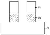
도 7은 본 발명의 제2실시예에 따른 비결정성 탄소막을 희생 하드마스크로 사용하는 도전패턴 형성을 위한 적층 구조를 도시한 단면도이다.7 is a cross-sectional view illustrating a laminated structure for forming a conductive pattern using an amorphous carbon film as a sacrificial hard mask according to a second embodiment of the present invention.
여기서, 제1실시예와 실질적으로 동일한 구성 요소에 대해서는 동일 부호를 사용한다.Here, the same reference numerals are used for the components substantially the same as in the first embodiment.
도 7을 참조하면, 기판(60) 상에 TiN 또는 폴리실리콘으로 이루어진 제1전도층(67)과 텅스텐으로 이루어진 제2전도층(61a) 및 하드마스크용 절연막(62a)이 적층되어 있다. 하드마스크용 절연막(62a)과 제2전도층(61a) 및 제1전도층(67)은 패터닝 공정을 통해 비트라인 등의 도전패턴을 이룬다. 하드마스크용 절연막(62a) 상에는 희생 하드마스크용 비결정성 탄소막(63a)이 적층되어 있고, 희생 하드마스크용 비결정성 탄소막(63a) 상에는 텅스텐막/질화막이 적층된 희생 하드마스크용 물질막(68)이 형성되어 있다. 희생 하드마스크용 물질막(68) 상에는 반사방지막(65a)이 적층되어 있으며, 반사방지막(65a) 상에는 포토레지스트 패턴(66a)이 형성되어 있다.Referring to FIG. 7, a first
희생 하드마스크용 물질막(68) 중 텅스텐막은 200Å ∼ 1000Å의 두께로 증착함으로써, 포토레지스트의 낮은 두께로도 충분히 식각될 수 있도록 한다.The tungsten film of the sacrificial hard
희생 하드마스크용 물질막(68) 중 텅스텐막 하부에 위치한 질화막은 상부의 텅스텐막이 충분히 마스크 역할을 하므로, 희생 하드마스크용 비결정성 탄소막(63a) 식각이 가능하도록 200Å 이상의 두께로 형성한다.The nitride film under the tungsten film of the sacrificial hard
질화막은 산화막, 질화막, 산화질화막의 단독 또는 조합된 구조로 치환하여 사용할 수 있다. 희생 하드마스크용 비결정성 탄소막(63a)은 1000Å 이상 보통, 2000Å 이상으로 충분히 두껍게 증착함으로써, 하부의 피식각층에 대한 식각선택비를 확보한다.The nitride film can be used by substituting a single or combined structure of an oxide film, a nitride film, and an oxynitride film. The
도 8은 본 발명의 제3실시예에 따른 비결정성 탄소막을 희생 하드마스크로 사용하는 도전패턴 형성을 위한 적층 구조를 도시한 단면도이다.FIG. 8 is a cross-sectional view illustrating a laminated structure for forming a conductive pattern using an amorphous carbon film as a sacrificial hard mask according to a third embodiment of the present invention.
여기서, 제1 및 제2실시예와 실질적으로 동일한 구성 요소에 대해서는 동일 부호를 사용한다.Here, the same reference numerals are used for components substantially the same as those of the first and second embodiments.
도 8을 참조하면, 기판(60) 상에 TiN 또는 폴리실리콘으로 이루어진 제1전도층(67)과 텅스텐으로 이루어진 제2전도층(61a) 및 하드마스크용 절연막(62a)이 적층되어 있다. 하드마스크용 절연막(62a)과 제2전도층(61a) 및 제1전도층(67)은 패터닝 공정을 통해 비트라인 등의 도전패턴을 이룬다. 하드마스크용 절연막(62a) 상에는 희생 하드마스크용 비결정성 탄소막(63a)이 적층되어 있고, 희생 하드마스크용 비결정성 탄소막(63a) 상에는 폴리실리콘막/질화막이 적층된 희생 하드마스크용 물질막(69)이 형성되어 있다. 희생 하드마스크용 물질막(69) 상에는 반사방지막(65a)이 적층되어 있으며, 반사방지막(65a) 상에는 포토레지스트 패턴(66a)이 형성되어 있다.Referring to FIG. 8, a first
희생 하드마스크용 물질막(69) 중 폴리실리콘막은 200Å ∼ 1000Å의 두께로 증착함으로써, 포토레지스트의 낮은 두께로도 충분히 식각될 수 있도록 한다.The polysilicon film in the sacrificial hard
희생 하드마스크용 물질막(69) 중 폴리실리콘막 하부에 위치한 질화막은 상부의 폴리실리콘막이 충분히 마스크 역할을 하므로, 희생 하드마스크용 비결정성 탄소막(63a) 식각이 가능하도록 200Å 이상의 두께로 형성한다.The nitride film under the polysilicon film of the sacrificial hard
질화막은 산화막, 질화막, 산화질화막의 단독 또는 조합된 구조로 치환하여 사용할 수 있다. 희생 하드마스크용 비결정성 탄소막(63a)은 1000Å 이상 보통, 2000Å 이상으로 충분히 두껍게 증착함으로써, 하부의 피식각층에 대한 식각선택비를 확보한다.The nitride film can be used by substituting a single or combined structure of an oxide film, a nitride film, and an oxynitride film. The
도 9는 본 발명의 제4실시예에 따른 비결정성 탄소막을 희생 하드마스크로 사용하는 도전패턴 형성을 위한 적층 구조를 도시한 단면도이다.9 is a cross-sectional view illustrating a laminated structure for forming a conductive pattern using an amorphous carbon film as a sacrificial hard mask according to a fourth embodiment of the present invention.
여기서, 제1 내지 제3실시예와 실질적으로 동일한 구성 요소에 대해서는 동일 부호를 사용한다.Here, the same reference numerals are used for the components substantially the same as the first to third embodiments.
도 9를 참조하면, 기판(60) 상에 TiN 또는 폴리실리콘으로 이루어진 제1전도층(67)과 텅스텐으로 이루어진 제2전도층(61a) 및 하드마스크용 절연막(62a)이 적층되어 있다. 하드마스크용 절연막(62a)과 제2전도층(61a) 및 제1전도층(67)은 패터닝 공정을 통해 비트라인 등의 도전패턴을 이룬다. 하드마스크용 절연막(62a) 상에는 질화막으로 이루어진 희생 하드마스크용 물질막(64a)이 형성되어 있고, 희생 하드마스크용 물질막(64a) 상에는 희생 하드마스크용 비결정성 탄소막(63a)이 적층되어 있다. 희생 하드마스크용 비결정성 탄소막(63a) 상에는 반사방지막(65a)이 적 층되어 있으며, 반사방지막(65a) 상에는 포토레지스트 패턴(66a)이 형성되어 있다.Referring to FIG. 9, a first
제4실시예에서는 반사방지막(65a)으로 무기기인 SiON을 사용하고, 그 바로 밑에 희생 하드마스크용 비결정성 탄소막(63a)이 위치하도록 하였다.In the fourth embodiment, SiON, which is an inorganic group, is used as the
여기서는 반사방지막의 역할과 희생 하드마스크로서의 역할을 하도록 한다. 이를 위해 포토레지스트의 낮은 두께로도 충분히 식각될 수 있도록 반사방지막(65a)을 200Å ∼ 1000Å의 두께로 증착한다.In this case, it serves as an anti-reflection film and a sacrificial hard mask. To this end, the
반사방지막(65a)과 희생 하드마스크용 물질막(64a)은 산화막, 질화막, 산화질화막의 단독 또는 조합된 구조로 치환하여 사용할 수 있다. 희생 하드마스크용 비결정성 탄소막(63a)은 1000Å 이상 보통, 2000Å 이상으로 충분히 두껍게 증착함으로써, 하부의 피식각층에 대한 식각선택비를 확보한다.The
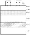
도 10a 내지 도 10d는 본 발명의 제5실시예에 따른 F2 또는 ArF 노광원을 이용한 반도체소자의 패턴 형성 공정을 도시한 단면도로서, 이를 참조하여 상세히 설명한다.10A to 10D are cross-sectional views illustrating a pattern forming process of a semiconductor device using an F2 or ArF exposure source according to a fifth embodiment of the present invention, and will be described in detail with reference to the drawings.
후술하는 본 발명의 제5실시예에서는 반도체소자의 스페이스 패턴(Space pattern) 예컨대, 콘택홀 패턴 형성 공정을 그 일예로 하여 설명하는 바, 본 발명의 적용 대상이 되는 콘택홀 패턴은 금속배선 콘택과 비트라인 또는 캐패시터의 스토리지 노드 콘택을 위한 소스/드레인 접합 등의 기판 내의 불순물 접합층과의 콘택 및 콘택 패드 형성을 위한 공정 등에 적용이 가능하다.In the fifth embodiment of the present invention described below, a process of forming a space pattern, for example, a contact hole pattern, of a semiconductor device is described as an example. The contact hole pattern to which the present invention is applied is a metal wiring contact. The present invention can be applied to a process for forming a contact pad and contact with an impurity junction layer in a substrate such as a source / drain junction for a storage node contact of a bit line or a capacitor.
또한, 이하의 실시예는 피식각층을 절연막으로 하는 공정인 소자분리 (Isolation)를 위한 트렌치(Trench) 형성 공정이나, 피식각층을 전도층으로 하는 공정 예컨대, 박막 트랜지스터(Thin film transistor)의 채널 형성 부분을 오픈시키기 위한 폴리실리콘을 식각하는 공정 등에도 적용이 가능하다. 즉, 본 발명의 이하의 실시예에서는 음각 패턴을 형성하는 공정으로의 적용을 나타낸다고 할 수 있다.In addition, the following embodiment is a trench formation process for device isolation, which is a process in which an etched layer is an insulating film, or a process in which a etched layer is a conductive layer, for example, channel formation of a thin film transistor. It is also applicable to a process of etching polysilicon to open a part. That is, in the following embodiments of the present invention it can be said that the application to the process of forming the intaglio pattern.
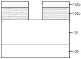
먼저, 도 10a에 도시된 바와 같이, 반도체소자를 형성하기 위한 여러 요소가 형성된 기판(100) 상에 피식각층으로 절연막(101)을 형성한다.First, as shown in FIG. 10A, an insulating
절연막(101)은 불순물이 도핑되거나(Doped) 또는 불순물이 도핑되지 않은(Undoped) 산화막 또는 질화막 등의 절연성 막을 포함한다.The insulating
이어서, 식각 공정시 절연막(101)의 이상 손실에 따른 패턴 변형을 방지하기 위해 절연막(101) 상에 희생 하드마스크용 비결정성 탄소막(102a)을 형성한다.Subsequently, in order to prevent pattern deformation due to abnormal loss of the insulating
이어서, 희생 하드마스크용 비결정성 탄소막(102a) 상에 희생 하드마스크용 물질막(103a)을 형성한다.Subsequently, a sacrificial hard
희생 하드마스크용 비결정성 탄소막(102a)은 포토레지스트와 유사한 탄소 성분으로 이루어져 있으므로, 포토레지스트 패턴으로 이를 식각하는 것은 공정의 효율성을 저하시킨다. 따라서, 희생 하드마스크용 비결정성 탄소막(102a)과 포토레지스트 패턴 사이에 추가의 희생 하드마스크를 사용하는 것이 바람직하다.Since the
여기서, 희생 하드마스크용 물질막(103a)은 폴리실리콘막, Al막, W막, WSix(x는 1 내지 2)막, WN막, Ti막, TiN막, TiSix(x는 1 내지 2)막, TiAlN막, TiSiN막, Pt막, Ir막, IrO2막, Ru막, RuO2막, Ag막, Au막, Co막, Au막, TaN막, CrN막, CoN막, MoN막, MoSix(x는 1 내지 2)막, Al2O3막, AlN막, PtSix(x는 1 내지 2)막 및 CrSix(x는 1 내지 2)막으로 이루어진 그룹으로부터 선택된 적어도 어느 하나의 박막을 포함한다.Here, the sacrificial hard
희생 하드마스크로 텅스텐막/질화막(산화막)/비결정성 탄소막의 구조를 사용한다면, 최상부의 텅스텐막의 두께를 300Å 이하로 얇게 하여 포토레지스트 패턴의 식각선택비에 영향을 받지 않도록 한다. 고해상도의 패턴 형성 공정이라 하더라도 ArF의 경우 포토레지스트를 1000Å 정도의 두께는 갖도록 한다. 즉, 1000Å 정도의 포토레지스트 패턴으로 300Å 이내의 텅스텐막을 식각하는 데에는 큰 어려움이 없을 것이다. 한편, 텅스텐 하부의 질화막(산화막)은 300Å ∼ 600Å 정도의 두께를 갖도록 하면, 300Å의 텅스텐막으로 식각할 수 있다. 이런 방식으로 텅스텐막과 질화막(산화막)을 차례로 식각한 후, 비결정성 탄소막을 식각한다. 이 때, N2 또는 O2 가스를 이용할 경우 질화막(산화막)과 비결정성 탄소막의 식각선택비를 20:1 이상으로 가져갈 수 있다.If the structure of the tungsten film / nitride film (oxide film) / amorphous carbon film is used as the sacrificial hard mask, the thickness of the uppermost tungsten film is made thinner than 300 GPa so as not to be affected by the etching selectivity of the photoresist pattern. Even in the high-resolution pattern formation process, ArF has a thickness of about 1000 GPa. That is, there will be no great difficulty in etching the tungsten film within 300 mW using a photoresist pattern of about 1000 mW. On the other hand, if the nitride film (oxide film) under the tungsten is made to have a thickness of about 300 kPa to 600 kPa, it can be etched into a 300 kW tungsten film. In this manner, the tungsten film and the nitride film (oxide film) are sequentially etched, and then the amorphous carbon film is etched. In this case, when the N2 or O2 gas is used, the etching selectivity of the nitride film (oxide film) and the amorphous carbon film may be 20: 1 or more.
20:1의 식각선택비는 300Å ∼ 600Å 두께의 질화막(산화막)으로 6000Å ∼ 12,000Å의 비결정성 탄소막을 식각할 수 있다는 것을 의미한다. 최소 6000Å의 두께를 갖는 비결정성 탄소막은 10,000Å 이상의 절연막(101)을 충분히 식각할 수 있게 한다.An etching selectivity ratio of 20: 1 means that an amorphous carbon film of 6000 mW to 12,000 mW can be etched with a nitride film (oxide film) having a thickness of 300 mW to 600 mW. An amorphous carbon film having a thickness of at least 6000 GPa enables sufficient etching of the insulating
이어서, 희생 하드마스크용 물질막(103a) 상에 패턴 형성을 위한 노광시 하 부 즉, 희생 하드마스크용 비결정성 탄소막(102a)의 광반사도가 높음으로 인해 난반사가 이루어져 원하지 않는 패턴이 형성되는 것을 방지하며, 희생 하드마스크용 물질막(103a)과 후속 포토레지스트의 접착력을 향상시킬 목적으로 반사방지막(104a, ARC)을 형성한다.Subsequently, due to the high light reflectivity under the exposure for forming the pattern on the sacrificial hard
여기서, 반사방지막(104a)은 포토레지스트와 그 식각 특성이 유사한 유기기의 물질을 이용하거나, SiON 등의 무기기를 이용할 수 있다.Here, the
이어서, 반사방지막(104a) 상에 F2 노광원용 또는 ArF 노광원용의 포토레지스트 예를 들어, COMA 또는 아크릴레이드를 사용하며, 이들을 스핀 코팅 등의 방법을 통해 적절한 두께로 도포한 다음, F2 노광원 또는 ArF 노광원과 게이트전극 폭을 정의하기 위한 소정의 레티클(도시하지 않음)을 이용하여 포토레지스트의 소정 부분을 선택적으로 노광하고, 현상 공정을 통해 노광 공정에 의해 노광되거나 혹은 노광되지 않은 부분을 잔류시킨 다음, 후세정 공정 등을 통해 식각 잔유물 등을 제거함으로써 포토레지스트 패턴(105a)을 형성한다.Subsequently, a photoresist for an F2 exposure source or an ArF exposure source, for example, COMA or acrylate, is used on the
계속해서, 도 10b에 도시된 바와 같이, 포토레지스트 패턴105b)을 식각마스크로 하는 선택적 식각 공정을 통해 반사방지막(104b)을 선택적으로 식각한다.Subsequently, as illustrated in FIG. 10B, the
이 때, 포토레지스트 패턴(105b)의 손실을 최소화하기 위해 Cl2, BCl3, CCl4 또는 HCl 등의 클로린계 가스를 사용한 플라즈마를 이용하여 식각 공정을 실시하거나, CF 계열의 가스를 사용할 경우 C/F의 비율이 낮은 가스 예컨대, CF4, C2F2, CHF3 및 CH2F2로 이루어진 그룹으로부터 선택된 어느 하나의 가스를 사용한 플라즈마를 이용하여 식각 공정을 실시하는 것이 바람직하다.In this case, in order to minimize the loss of the
이는 반사방지막(104b) 식각 시에는 CD의 조절이 용이해야 하므로 폴리머를 거의 발생시키지 않는 조건으로 식각을 진행하기 위한 것이다.This is because the CD should be easily controlled during the
이어서, 포토레지스트 패턴(105b)을 식각마스크로 희생 하드마스크용 물질막(103a)을 식각하여 제1희생 하드마스크(103b)를 형성한다.Subsequently, the sacrificial hard
이하, 희생 하드마스크용 물질막(103a) 식각 공정을 구체적으로 살펴본다.Hereinafter, an etching process of the
희생 하드마스크용 물질막(103a)이 W막, WSix막 또는 WN막과 같이 텅스텐(W)을 포함하는 박막인 경우, SF6/N2의 혼합 가스를 사용한 플라즈마를 이용하며, 이 때 SF6/N2의 혼합비율이 0.10 ∼ 0.60인 것을 사용하는 것이 바람직하다.When the
희생 하드마스크용 물질막(103a)이 폴리실리콘막 또는 Ti막, TiN막, TiSix막, TiAlN막 또는 TiSiN막과 같이 티타늄(Ti)을 포함하는 박막인 경우, 클로린 계열의 가스 특히, Cl2를 주식각가스로 하며, 이 때 식각 프로파일의 제어를 위해 산소(O2) 또는 CF 가스를 적절히 첨가하여 사용한다.When the sacrificial hard
희생 하드마스크용 물질막(103a)이 Pt, Ir, Ru 등의 귀금속 또는 이들의 산화물을 포함하는 경우 클로린 계열 또는 플로린 계열의 가스를 사용한 플라즈마를 이용하며, 이 때 식각 프로파일의 제어를 위해서는 높은 이온에너지가 필요하므로 이를 위해 저압 및 고 바이어스 파워 조건을 유지하도록 하는 것이 바람직하다.When the sacrificial hard
도 10c에 도시된 바와 같이, 적어도(포토레지스트 패턴(105b)과 반사방지막(104b)은 대부분 식각 과정에서 제거가 되나 그 일부가 잔류될 수 있는 바, 포토레지스트 패턴(105b)과 반사방지막(104b)의 제거를 위한 별도의 포토레지스트 스트립 공정을 실시하지 않는 경우 잔류하는 포토레지스트 패턴(105b)과 반사방지막(104b)이 식각마스크 역할을 할 수 있으므로 '적어도'라고 표현함) 제1희생 하드마스크(103b)를 식각마스크로 희생 하드마스크용 비결정성 탄소막(102a)을 식각하여 제2희생 하드마스크(102b)를 형성한다. 이 때, N2 또는 O2 가스를 이용한다.As shown in FIG. 10C, at least (the
상기한 바와 같이, 제1희생 하드마스크(103b)와 희생 하드마스크용 비결정성 탄소막(102a)의 식각선택비가 높기 때문에 제2희생 하드마스크(102b)의 두께를 충분히 확보할 수 있다.As described above, since the etching selectivity of the first sacrificial
이어서, 도 10d에 도시된 바와 같이, 제2희생 하드마스크(102c)를 식각마스크로 절연막(101)를 선택적으로 식각하여 기판(100) 구체적으로는 도전구조의 표면 또는 그 상부를 노출시키는 콘택홀(106)을 형성한다.Subsequently, as shown in FIG. 10D, the second sacrificial
이어서, 잔류하는 제2희생 하드마스크(102c)를 제거한다. 제2희생 하드마스크(102c)는 비결정성 탄소막으로 이루어지므로 산소 플라즈마를 이용하여 간단히 제거할 수 있다.Subsequently, the remaining second sacrificial
이 때, 제2희생 하드마스크(102c)의 두께를 충분히 확보할 수 있으므로, 제2희생 하드마스크(102c)의 식각 마스크로서의 특성울 유지할 수 있어 희생 하드마스크의 손실로 인한 콘택홀(106)의 CD의 증가 또는 감소 등의 패턴 변형을 방지할 수 있다.At this time, the thickness of the second sacrificial
전술한 절연막(101)으로 주로 산화막 계열을 이용하는 바, 산화막에 대한 식각 조건을 보다 구체적으로 살펴 본다.Since the oxide film is mainly used as the insulating
산화막 식각시 통상적으로 사용되는 CF4, CHF3, CH2F2, C4F6, C4F8, C3F8 또는 C5F8 등을 CF계열(Fluorocarbon)의 가스를 사용하며, 이 때 MERIE(Magnetic Enhancement Reactive Ion Etching) 방식의 에쳐(Etcher)에서 CF가스의 플로우율을 20SCCM ∼ 100SCCM으로 하고 1000W ∼ 2500W 정도의 파워를 사용한다.CF4 , CHF3 , CH2 F2 , C4 F6 , C4 F8 , C3 F8, or C5 F8, etc., which are commonly used in etching an oxide layer, use a CF-based gas. In this case, the flow rate of CF gas is set at 20 SCCM to 100 SCCM in the etchant of MERIE (Magnetic Enhancement Reactive Ion Etching), and power of about 1000 W to 2500 W is used.
이 때, 에쳐 내의 압력을 25mTorr ∼ 70mTorr로 유지하고, 캐소드(Cathode) 온도를 -20℃ ∼ +60℃ 정도로 유지하며, 식각 프로파일을 제어할 수 있도록 상기 CF 가스의 65% ∼ 80%의 플로우율로 산소 가스를 더 첨가할 수 있다.At this time, the pressure in the archer is maintained at 25 mTorr to 70 mTorr, the cathode temperature is maintained at about -20 ° C to + 60 ° C, and the flow rate of 65% to 80% of the CF gas is controlled to control the etching profile. Oxygen gas can be added further.
도 11은 본 발명의 제6실시예에 따른 비결정성 탄소막을 희생 하드마스크로 사용하는 콘택홀 형성을 위한 적층 구조를 도시한 단면도이다.FIG. 11 is a cross-sectional view illustrating a laminated structure for forming a contact hole using an amorphous carbon film as a sacrificial hard mask according to a sixth embodiment of the present invention.
여기서, 제5실시예와 실질적으로 동일한 구성 요소에 대해서는 동일 부호를 사용한다.Here, the same reference numerals are used for the components substantially the same as in the fifth embodiment.
도 11을 참조하면, 기판(100) 상에 피식각층인 절연막(101)과 희생 하드마스크용 물질막(103a)이 적층되어 있으며, 희생 하드마스크용 물질막(103a) 상에는 희생 하드마스크용 비결정성 탄소막(102a)이 적층되어 있다. 희생 하드마스크용 비결정성 탄소막(102a) 상에는 반사방지막(104a)이 적층되어 있으며, 반사방지막(104a) 상에는 포토레지스트 패턴(105a)이 형성되어 있다.Referring to FIG. 11, an insulating
제6실시예에서는 반사방지막(104a)으로 무기기인 SiON을 사용하고, 그 바로 밑에 희생 하드마스크용 비결정성 탄소막(102a)이 위치하도록 하였다.In the sixth embodiment, SiON, which is an inorganic group, is used as the
여기서는 반사방지막의 역할과 희생 하드마스크로서의 역할을 하도록 한다. 이를 위해 포토레지스트의 낮은 두께로도 충분히 식각될 수 있도록 반사방지막(104a)을 200Å ∼ 1000Å의 두께로 증착한다.In this case, it serves as an anti-reflection film and a sacrificial hard mask. To this end, the
반사방지막(104a)과 희생 하드마스크용 물질막(103a)은 산화막, 질화막, 산화질화막의 단독 또는 조합된 구조로 치환하여 사용할 수 있다. 희생 하드마스크용 비결정성 탄소막(102a)은 1000Å 이상 보통, 2000Å 이상으로 충분히 두껍게 증착함으로써, 하부의 피식각층에 대한 식각선택비를 확보한다.The
도 12은 본 발명의 제7실시예에 따른 비결정성 탄소막을 희생 하드마스크로 사용하는 콘택홀 형성을 위한 적층 구조를 도시한 단면도이다.12 is a cross-sectional view illustrating a laminated structure for forming a contact hole using an amorphous carbon film as a sacrificial hard mask according to a seventh embodiment of the present invention.
여기서, 제5 및 제 6실시예와 실질적으로 동일한 구성 요소에 대해서는 동일 부호를 사용한다.Here, the same reference numerals are used for components substantially the same as those of the fifth and sixth embodiments.
도 12를 참조하면, 기판(100) 상에 피식각층인 절연막(101)이 형성되어 있고, 절연막(101) 상에는 희생 하드마스크용 비결정성 탄소막(102a)이 적층되어 있고, 희생 하드마스크용 비결정성 탄소막(102a) 상에는 텅스텐막/질화막이 적층된 희생 하드마스크용 물질막(107)이 형성되어 있다. 희생 하드마스크용 물질막(107) 상에는 반사방지막(104a)이 적층되어 있으며, 반사방지막(104a) 상에는 포토레지스트 패턴(105a)이 형성되어 있다.Referring to FIG. 12, an insulating
희생 하드마스크용 물질막(107) 중 텅스텐막은 200Å ∼ 1000Å의 두께로 증 착함으로써, 포토레지스트의 낮은 두께로도 충분히 식각될 수 있도록 한다.The tungsten film of the sacrificial hard
희생 하드마스크용 물질막(107) 중 텅스텐막 하부에 위치한 질화막은 상부의 텅스텐막이 충분히 마스크 역할을 하므로, 희생 하드마스크용 비결정성 탄소막(102a) 식각이 가능하도록 200Å 이상의 두께로 형성한다.The nitride film under the tungsten film of the sacrificial hard
질화막은 산화막, 질화막, 산화질화막의 단독 또는 조합된 구조로 치환하여 사용할 수 있다. 희생 하드마스크용 비결정성 탄소막(102a)은 1000Å 이상 보통, 2000Å 이상으로 충분히 두껍게 증착함으로써, 하부의 피식각층에 대한 식각선택비를 확보한다.The nitride film can be used by substituting a single or combined structure of an oxide film, a nitride film, and an oxynitride film. The
도 13는 본 발명의 제8실시예에 따른 비결정성 탄소막을 희생 하드마스크로 사용하는 콘택홀 형성을 위한 적층 구조를 도시한 단면도이다.FIG. 13 is a cross-sectional view illustrating a laminated structure for forming a contact hole using an amorphous carbon film as a sacrificial hard mask according to an eighth embodiment of the present invention.
여기서, 제5 내지 제7실시예와 실질적으로 동일한 구성 요소에 대해서는 동일 부호를 사용한다.Here, the same reference numerals are used for components substantially the same as those of the fifth to seventh embodiments.
도 13을 참조하면, 기판(100) 상에 피식각층인 절연막(101)이 형성되어 있고, 절연막(101) 상에는 희생 하드마스크용 비결정성 탄소막(102a)이 적층되어 있고, 희생 하드마스크용 비결정성 탄소막(102a) 상에는 폴리실리콘막/질화막이 적층된 희생 하드마스크용 물질막(108)이 형성되어 있다. 희생 하드마스크용 물질막(108) 상에는 반사방지막(104a)이 적층되어 있으며, 반사방지막(104a) 상에는 포토레지스트 패턴(105a)이 형성되어 있다.Referring to FIG. 13, an insulating
희생 하드마스크용 물질막(108) 중 폴리실리콘막은 200Å ∼ 1000Å의 두께로 증착함으로써, 포토레지스트의 낮은 두께로도 충분히 식각될 수 있도록 한다.The polysilicon film of the sacrificial hard
희생 하드마스크용 물질막(108) 중 폴리실리콘막 하부에 위치한 질화막은 상부의 폴리실리콘막이 충분히 마스크 역할을 하므로, 희생 하드마스크용 비결정성 탄소막(102a) 식각이 가능하도록 200Å 이상의 두께로 형성한다.The nitride film under the polysilicon layer of the sacrificial hard
질화막은 산화막, 질화막, 산화질화막의 단독 또는 조합된 구조로 치환하여 사용할 수 있다. 희생 하드마스크용 비결정성 탄소막(102a)은 1000Å 이상 보통, 2000Å 이상으로 충분히 두껍게 증착함으로써, 하부의 피식각층에 대한 식각선택비를 확보한다.The nitride film can be used by substituting a single or combined structure of an oxide film, a nitride film, and an oxynitride film. The
이하에서는 실제 DRAM(Dynamic Random Access Memory) 공정의 예를 통해 홀 패턴 형성을 위한 구조를 살펴 본다.Hereinafter, a structure for forming a hole pattern will be described through an example of an actual DRAM (Dynamic Random Access Memory) process.
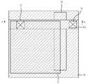
도 14는 금속배선 형성을 위한 마스크 패턴이 형성된 반도체소자를 도시한 평면도이다.14 is a plan view illustrating a semiconductor device in which a mask pattern for forming metal wiring is formed.
도 14를 참조하면, 게이트전극(G)이 형성되어 있고, 게이트전극(G) 상부에서 게이트전극(G)과 교차하는 방향으로 비트라인(B/L)이 형성되어 있다. 게이트전극(G)의 측면에 얼라인되어 형성된 셀콘택 플러그(도시하지 않음)와, 셀콘택 플러그에 콘택된 스토리지노드용 콘택 플러그(도시하지 않음)와, 스토리지노드용 콘택 플러그 접속된 스토리지노드(도시하지 않음)와, 스토리지노드 상부의 유전체막(도시하지 않음)과, 유전체막 상의 플레이트전극(P)이 일련의 공정을 통해 형성되어 있다.Referring to FIG. 14, a gate electrode G is formed, and a bit line B / L is formed in a direction crossing the gate electrode G on the gate electrode G. Referring to FIG. A cell contact plug (not shown) formed on the side surface of the gate electrode G, a storage node contact plug (not shown) contacted to the cell contact plug, a storage node contact plug connected to the storage node ( Not shown), a dielectric film (not shown) on the storage node, and a plate electrode P on the dielectric film are formed through a series of processes.
플레이트전극(P) 상부에는 금속배선 콘택 형성을 위한 마스크 패턴(M)이 형성되어 있다.A mask pattern M is formed on the plate electrode P to form a metal wiring contact.
한편, 게이트전극(G)을 포함한 비트라인(B/L)과 플레이트전극(P) 등은 모두 신호 또는 전원 라인과의 접속을 위해 금속배선과 접속되어야 한다.On the other hand, both the bit line (B / L) and the plate electrode (P) including the gate electrode (G) should be connected to the metal wiring for the connection to the signal or power line.
마스크 패턴(M)은 플레이트 전극(P)의 금속배선을 위한 콘택(A)과 비트라인(B/L)의 금속배선을 위한 콘택(B) 형성을 위한 것이다.The mask pattern M is for forming a contact A for metal wiring of the plate electrode P and a contact B for metal wiring of the bit line B / L.
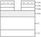
도 15는 도 14를 a-a' 방향으로 절취한 단면도이다.15 is a cross-sectional view taken along the line a-a 'of FIG. 14.
도 15를 참조하면, 기판(150) 상에 게이트전극(G)이 형성되어 있다. 게이트전극(G)은 게이트 산화막(151)과 게이트 전도막(152)과 게이트 하드마스크(153)의 적층 구조와 그 측면의 스페이서(154)를 구비한다. 게이트전극(G)은 제1층간절연막(155)에 의해 둘러 쌓여 있으며, 제1층간절연막(155)을 관통하여 기판(150)의 불순물 확산영역과 콘택되며 게이트 하드마스크(153)와 평탄화되어 아이솔레이션(Isolation)이 이루어진 셀콘택 플러그(156)가 형성되어 있다.Referring to FIG. 15, a gate electrode G is formed on the
셀콘택 플러그(156) 상에는 제2층간절연막(157)이 형성되어 있으며, 제2층간절연막(157) 상에는 제2층간절연막(157)을 관통하여 도면에서 도시되지 않은 셀콘택 플러그와 전기적으로 접속된 비트라인(B/L)이 형성되어 있다.A second
비트라인(B/L)은 비트라인 전도막(158)과 비트라인 하드마스크(159)의 적층 구조와 그 측면의 스페이서(도시하지 않음)를 구비한다.The bit line B / L includes a stack structure of the bit line
비트라인(B/L) 상에는 제3층간절연막(160)이 형성되어 있다. 제3층간절연막(160) 상에는 제3층간절연막(160)과 제2층간절연막(157)을 관통하여 도면에서 도시되지 않은 셀콘택 플러그와 전기적으로 접속된 스토리지노드용 콘택 플러그가 형성되어 있다.The third
스토리지노드용 콘택 플러그 상에는 스토리지노드(161)와 유전체막(162) 및 플레이트전극(163)이 차례로 형성되어 셀 캐패시터를 이룬다. 한편, 셀 캐패시터가 형성되지 않는 부분에서는 제4층간절연막(164)이 형성되어 있다.The
캐패시터 및 제4층간절연막(164) 상에는 제5층간절연막(165)이 형성되어 있으며, 제5층간절연막(165) 상에는 희생 하드마스크용 비결정성 탄소막(166)이 형성되어 있고, 희생 하드마스크용 비결정성 탄소막(166) 상에는 희생 하드마스크용 물질막(167)이 형성되어 있다. 희생 하드마스크용 물질막(167) 상에는 반사방지막(168)이 적층되어 있으며, 반사방지막(168) 상에는 포토레지스트 패턴(169)이 형성되어 있다.A fifth
플레이트전극(163)의 금속배선 형성을 위한 식각 부위는 도면부호 '170'과 같이 제5층간절연막(170) 만을 포함하므로 별 다른 상관이 없으나, 비트라인(B/L) 금속배선을 형성을 위한 식각 부위는 도면부호 '171'과 같이 제5층간절연막(165)과 제4층간절연막(164) 및 비트라인 하드마스크(159)를 포함하므로 식각 타겟이 상당히 큼을 알 수 있다.Since the etching portion for forming the metal wiring of the
특히, 제4층간절연막(164)의 경우 캐패시터의 수직 높이에 달하므로 그 두께만으로 20,000Å 정도 된다고 볼 수 있다. 따라서, 도면부호 '171'의 식각 타겟은 30,000 정도가 됨을 알 수 있다.In particular, since the fourth
따라서, 종래의 희생 하드마스크 만을 사용하는 방식에서는 특히, 80nm 이하의 디자인 룰이 적용되는 반도체소자 제조 공정시 원하는 콘택홀 패턴을 형성하는 것이 사실상 불가능하다.Therefore, in the conventional method using only the sacrificial hard mask, it is virtually impossible to form a desired contact hole pattern in the semiconductor device manufacturing process to which a design rule of 80 nm or less is applied.
하지만, 10,000Å 이상의 두께를 확보할 수 있는 희생 하드마스크용 비결정성 탄소막(166)를 사용하게 되면, 이러한 깊은 콘택홀 형성시에도 패턴 변형이 거의 없이 원하는 패턴 형성이 가능하다.However, when the
도 16은 스토리지노드 콘택 형성을 위한 마스크 패턴이 형성된 반도체소자를 도시한 평면도이다.16 is a plan view illustrating a semiconductor device in which a mask pattern for forming a storage node contact is formed.
도 16을 참조하면, 게이트전극 G1과 G2가 일방향으로 일정 간격을 갖고 배열되어 있고, 게이트전극(G1, G2) 상부에서 게이트전극(G1, G2)과 교차하는 방향으로 비트라인(B/L1, B/L2)이 형성되어 있다. 게이트전극(G1, G2)의 측면에 얼라인되어 셀콘택 플러그(도시하지 않음)가 형성되어 있으며, 비트라인(B/L1, B/L2) 상부에는 스토리지노드용 콘택홀 형성을 위한 마스크 패턴(M)이 형성되어 있다.Referring to FIG. 16, the gate electrodes G1 and G2 are arranged at regular intervals in one direction, and the bit lines B / L1 and G2 intersect the gate electrodes G1 and G2 on the gate electrodes G1 and G2. B / L2) is formed. Cell contact plugs (not shown) are formed on the side surfaces of the gate electrodes G1 and G2, and mask patterns for forming contact holes for storage nodes are formed on the bit lines B / L1 and B / L2. M) is formed.
마스크 패턴(M)은 스토리지노드용 콘택홀 형성을 위해 비트라인(B/L1, B/L2)의 측면에 각각 얼라인되어 도면부호 'C'와 같은 부분에서 셀콘택 플러그를 노출시키기 위한 것이다.The mask pattern M is aligned on the side surfaces of the bit lines B / L1 and B / L2 to form contact holes for the storage node, and exposes the cell contact plugs at portions such as 'C'.
도 17은 도 16을 b-b' 방향으로 절취한 단면도이다.17 is a cross-sectional view taken along the line b-b 'of FIG. 16.
도 17을 참조하면, 기판(200) 상에 게이트전극이 형성되어 있는 바, 도 16을 b-b' 방향으로 절취한 단면에서는 게이트전극이 나타나지 않는다.Referring to FIG. 17, since the gate electrode is formed on the
게이트전극은 제1층간절연막(201)에 의해 둘러 쌓여 있으며, 제1층간절연막(201)을 관통하여 기판(200)의 불순물 확산영역과 콘택되며 게이트 하드마스크(도시하지 않음)와 평탄화되어 아이솔레이션이 이루어진 셀콘택 플러그(202)가 형성되어 있다.The gate electrode is surrounded by the first
셀콘택 플러그(202) 상에는 제2층간절연막(203)이 형성되어 있으며, 제2층간절연막(203) 상에는 제2층간절연막(203)을 관통하여 도면에서 도시되지 않은 셀콘택 플러그와 전기적으로 접속된 비트라인(B/L)이 형성되어 있다.A second
비트라인(B/L)은 비트라인 전도막(204)과 비트라인 하드마스크(205)의 적층 구조와 그 측면의 스페이서(S)를 구비한다.The bit line B / L includes a stacked structure of the bit line
비트라인(B/L) 상에는 제3층간절연막(206)이 형성되어 있다. 제3층간절연막(160) 상에는 스토리지노드 형성시 하부의 어택 방지를 위한 스토리지노드용 하드마스크(207)와 PE-TEOS(플라즈마 화학기상증착(Plasma Enhanced Chemical Vapor Deposition; 이하 PECVD라 함) 방식으로 TEOS(Tetra Ethyl Ortho SIlicate) 소스를 사용하여 형성한 산화막)이 적층되어 있다. PE_TEOS막(208) 상에는 식각정지막(209)이 형성되어 있으며, 식각정지막(209) 상에는 질화막 또는 산화막을 이용한 희생 하드마스크용 절연막(210)이 형성되어 있다.A third
희생 하드마스크용 절연막(210) 상에는 희생 하드마스크용 비결정성 탄소막(211)이 형성되어 있고, 희생 하드마스크용 비결정성 탄소막(211) 상에는 희생 하드마스크용 실리콘산화질화막(212)이 형성되어 있다. 희생 하드마스크용 실리콘산화질화막(212) 상에는 희생 하드마스크용 텅스텐막(213)이 형성되어 있다.A sacrificial hard mask
희생 하드마스크용 텅스텐막(213) 상에는 반사방지막(214)이 적층되어 있으며, 반사방지막(214) 상에는 포토레지스트 패턴(215)이 형성되어 있다.An
스토리지노드용 콘택홀 형성 공정의 경우 오버랩 마진이 상당히 부족하고 그 식각 타겟 또한 크므로 10,000Å 이상의 두께를 확보할 수 있는 희생 하드마스크용 비결정성 탄소막(212)를 사용하게 되면, 패턴 변형이 거의 없이 원하는 패턴 형성이 가능하다.In the case of the contact hole forming process for the storage node, since the overlap margin is considerably insufficient and the etching target is also large, when using the
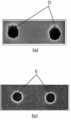
도 18은 ArF 포토리소그라피 공정을 적용한 콘택홀 형성 후의 종래기술과 본발명의 차이점을 비교 도시한 평면 사진이다.FIG. 18 is a planar photograph illustrating the difference between the prior art and the present invention after contact hole formation using the ArF photolithography process.
도 18의 (a)는 종래의 ArF 포토리소그라피 공정을 적용하여 형성한 콘택홀을 나타내며, 'D'와 같이 콘택홀 패턴의 변형이 발생한 것을 확인할 수 있다. 반면, 도 18의 (b)의 비결정성 탄소막을 희생 하드마스크로 사용하고 ArF 포토리소그라피 공정을 적용하여 형성한 콘택홀을 나타내며, 'E'와 같이 콘택홀 패턴의 변형이 발생하지 않음을 확인할 수 있다.
Figure 18 (a) shows a contact hole formed by applying the conventional ArF photolithography process, it can be seen that the deformation of the contact hole pattern as shown in 'D'. On the other hand, it shows a contact hole formed by using the amorphous carbon film of Figure 18 (b) as a sacrificial hard mask and applying the ArF photolithography process, it can be seen that the deformation of the contact hole pattern does not occur as 'E' have.
상기한 바와 같이 이루어지는 본 발명은, 기존의 희생 하드마스크 물질과는 다른 비결정성 탄소막을 희생 하드마스크로 사용하며, 여기에 산화막/질화막 또는/및 폴리실리콘/텅스텐 등의 희생 하드마스크와 적층 구조로 사용함으로써, 포토레지스트의 낮은 식각선택비로 인한 ArF 또는 F2 등의 노광원을 이용한 포토리소그라피 공정에 의한 패턴 형성시, 패턴 변형을 방지할 수 있음을 실시예를 통해 알아보았다.
The present invention made as described above uses an amorphous carbon film different from the existing sacrificial hard mask material as a sacrificial hard mask, and has a laminated structure with a sacrificial hard mask such as an oxide film / nitride film and / or polysilicon / tungsten. By using the present invention, it was found through the examples that pattern deformation can be prevented during pattern formation by a photolithography process using an exposure source such as ArF or F2 due to the low etching selectivity of the photoresist.
이상에서 설명한 본 발명은 전술한 실시예 및 첨부된 도면에 의해 한정되는 것이 아니고, 본 발명의 기술적 사상을 벗어나지 않는 범위 내에서 여러 가지 치 환, 변형 및 변경이 가능하다는 것이 본 발명이 속하는 기술분야에서 통상의 지식을 가진 자에게 있어 명백할 것이다.
The present invention described above is not limited to the above-described embodiments and the accompanying drawings, and various substitutions, modifications, and changes can be made without departing from the technical spirit of the present invention. It will be apparent to those of ordinary skill in Esau.
전술한 본 발명은, F2 또는 ArF 등의 노광원을 사용하는 사진식각 공정에 따른 포토레지스트 패턴의 변형과 손실을 방지할 수 있어, 반도체소자의 수율을 크게 향상시킬 수 있는 효과가 있다.The present invention described above can prevent the deformation and loss of the photoresist pattern according to the photolithography process using an exposure source such as F2 or ArF, so that the yield of the semiconductor device can be greatly improved.
Claims (19)
Translated fromKoreanPriority Applications (3)
| Application Number | Priority Date | Filing Date | Title |
|---|---|---|---|
| KR1020040059535AKR100704470B1 (en) | 2004-07-29 | 2004-07-29 | Method for manufacturing semiconductor device using amorphous carbon film as sacrificial hard mask |
| JP2005170855AJP2006041486A (en) | 2004-07-29 | 2005-06-10 | Method for manufacturing semiconductor device using amorphous carbon film as sacrificial hard mask |
| US11/149,326US7446049B2 (en) | 2004-07-29 | 2005-06-10 | Method for fabricating semiconductor device using amorphous carbon layer as sacrificial hard mask |
Applications Claiming Priority (1)
| Application Number | Priority Date | Filing Date | Title |
|---|---|---|---|
| KR1020040059535AKR100704470B1 (en) | 2004-07-29 | 2004-07-29 | Method for manufacturing semiconductor device using amorphous carbon film as sacrificial hard mask |
Publications (2)
| Publication Number | Publication Date |
|---|---|
| KR20060010932A KR20060010932A (en) | 2006-02-03 |
| KR100704470B1true KR100704470B1 (en) | 2007-04-10 |
Family
ID=35732884
Family Applications (1)
| Application Number | Title | Priority Date | Filing Date |
|---|---|---|---|
| KR1020040059535AExpired - Fee RelatedKR100704470B1 (en) | 2004-07-29 | 2004-07-29 | Method for manufacturing semiconductor device using amorphous carbon film as sacrificial hard mask |
Country Status (3)
| Country | Link |
|---|---|
| US (1) | US7446049B2 (en) |
| JP (1) | JP2006041486A (en) |
| KR (1) | KR100704470B1 (en) |
Cited By (1)
| Publication number | Priority date | Publication date | Assignee | Title |
|---|---|---|---|---|
| US10236185B2 (en) | 2016-11-25 | 2019-03-19 | Samsung Electronics Co., Ltd. | Method of forming patterns for semiconductor device |
Families Citing this family (107)
| Publication number | Priority date | Publication date | Assignee | Title |
|---|---|---|---|---|
| US7151040B2 (en)* | 2004-08-31 | 2006-12-19 | Micron Technology, Inc. | Methods for increasing photo alignment margins |
| US7910288B2 (en) | 2004-09-01 | 2011-03-22 | Micron Technology, Inc. | Mask material conversion |
| US7115525B2 (en) | 2004-09-02 | 2006-10-03 | Micron Technology, Inc. | Method for integrated circuit fabrication using pitch multiplication |
| US7655387B2 (en) | 2004-09-02 | 2010-02-02 | Micron Technology, Inc. | Method to align mask patterns |
| US7390746B2 (en) | 2005-03-15 | 2008-06-24 | Micron Technology, Inc. | Multiple deposition for integration of spacers in pitch multiplication process |
| US7253118B2 (en)* | 2005-03-15 | 2007-08-07 | Micron Technology, Inc. | Pitch reduced patterns relative to photolithography features |
| US7611944B2 (en) | 2005-03-28 | 2009-11-03 | Micron Technology, Inc. | Integrated circuit fabrication |
| US7429536B2 (en) | 2005-05-23 | 2008-09-30 | Micron Technology, Inc. | Methods for forming arrays of small, closely spaced features |
| US7560390B2 (en)* | 2005-06-02 | 2009-07-14 | Micron Technology, Inc. | Multiple spacer steps for pitch multiplication |
| US7396781B2 (en)* | 2005-06-09 | 2008-07-08 | Micron Technology, Inc. | Method and apparatus for adjusting feature size and position |
| US7857982B2 (en)* | 2005-07-19 | 2010-12-28 | Micron Technology, Inc. | Methods of etching features into substrates |
| US7413981B2 (en)* | 2005-07-29 | 2008-08-19 | Micron Technology, Inc. | Pitch doubled circuit layout |
| US8123968B2 (en)* | 2005-08-25 | 2012-02-28 | Round Rock Research, Llc | Multiple deposition for integration of spacers in pitch multiplication process |
| US7816262B2 (en) | 2005-08-30 | 2010-10-19 | Micron Technology, Inc. | Method and algorithm for random half pitched interconnect layout with constant spacing |
| US7829262B2 (en)* | 2005-08-31 | 2010-11-09 | Micron Technology, Inc. | Method of forming pitch multipled contacts |
| US7557032B2 (en)* | 2005-09-01 | 2009-07-07 | Micron Technology, Inc. | Silicided recessed silicon |
| US7776744B2 (en)* | 2005-09-01 | 2010-08-17 | Micron Technology, Inc. | Pitch multiplication spacers and methods of forming the same |
| US7393789B2 (en)* | 2005-09-01 | 2008-07-01 | Micron Technology, Inc. | Protective coating for planarization |
| US7416943B2 (en)* | 2005-09-01 | 2008-08-26 | Micron Technology, Inc. | Peripheral gate stacks and recessed array gates |
| US7572572B2 (en) | 2005-09-01 | 2009-08-11 | Micron Technology, Inc. | Methods for forming arrays of small, closely spaced features |
| US7759197B2 (en) | 2005-09-01 | 2010-07-20 | Micron Technology, Inc. | Method of forming isolated features using pitch multiplication |
| US7687342B2 (en)* | 2005-09-01 | 2010-03-30 | Micron Technology, Inc. | Method of manufacturing a memory device |
| JP4507120B2 (en) | 2005-11-11 | 2010-07-21 | エルピーダメモリ株式会社 | Manufacturing method of semiconductor integrated circuit device |
| KR100724630B1 (en)* | 2006-01-06 | 2007-06-04 | 주식회사 하이닉스반도체 | Manufacturing Method of Semiconductor Device |
| US7563688B2 (en)* | 2006-02-24 | 2009-07-21 | Hynix Semiconductor Inc. | Method for fabricating capacitor in semiconductor device |
| US7842558B2 (en)* | 2006-03-02 | 2010-11-30 | Micron Technology, Inc. | Masking process for simultaneously patterning separate regions |
| US7476933B2 (en) | 2006-03-02 | 2009-01-13 | Micron Technology, Inc. | Vertical gated access transistor |
| US7598024B2 (en)* | 2006-03-08 | 2009-10-06 | Asml Netherlands B.V. | Method and system for enhanced lithographic alignment |
| US7662718B2 (en)* | 2006-03-09 | 2010-02-16 | Micron Technology, Inc. | Trim process for critical dimension control for integrated circuits |
| US7244313B1 (en) | 2006-03-24 | 2007-07-17 | Applied Materials, Inc. | Plasma etch and photoresist strip process with intervening chamber de-fluorination and wafer de-fluorination steps |
| US7902074B2 (en) | 2006-04-07 | 2011-03-08 | Micron Technology, Inc. | Simplified pitch doubling process flow |
| US7510976B2 (en)* | 2006-04-21 | 2009-03-31 | Applied Materials, Inc. | Dielectric plasma etch process with in-situ amorphous carbon mask with improved critical dimension and etch selectivity |
| US8003310B2 (en) | 2006-04-24 | 2011-08-23 | Micron Technology, Inc. | Masking techniques and templates for dense semiconductor fabrication |
| US7488685B2 (en) | 2006-04-25 | 2009-02-10 | Micron Technology, Inc. | Process for improving critical dimension uniformity of integrated circuit arrays |
| US7795149B2 (en) | 2006-06-01 | 2010-09-14 | Micron Technology, Inc. | Masking techniques and contact imprint reticles for dense semiconductor fabrication |
| US7723009B2 (en) | 2006-06-02 | 2010-05-25 | Micron Technology, Inc. | Topography based patterning |
| JP2008028022A (en)* | 2006-07-19 | 2008-02-07 | Tokyo Electron Ltd | Plasma etching method and computer readable storage medium |
| US8129282B2 (en)* | 2006-07-19 | 2012-03-06 | Tokyo Electron Limited | Plasma etching method and computer-readable storage medium |
| US20080124912A1 (en)* | 2006-08-01 | 2008-05-29 | Taiwan Semiconductor Manufacturing Co., Ltd. | Semiconductor methods |
| US7611980B2 (en) | 2006-08-30 | 2009-11-03 | Micron Technology, Inc. | Single spacer process for multiplying pitch by a factor greater than two and related intermediate IC structures |
| KR100913004B1 (en)* | 2006-09-06 | 2009-08-20 | 주식회사 하이닉스반도체 | Trench Formation Method for Semiconductor Devices |
| US7666578B2 (en)* | 2006-09-14 | 2010-02-23 | Micron Technology, Inc. | Efficient pitch multiplication process |
| KR100772706B1 (en) | 2006-09-28 | 2007-11-02 | 주식회사 하이닉스반도체 | Method for manufacturing contact hole of semiconductor device |
| EP2085823B1 (en)* | 2006-10-12 | 2013-01-16 | Nissan Chemical Industries, Ltd. | Method for manufacturing semiconductor device using quadruple-layer laminate |
| KR100792412B1 (en) | 2006-12-27 | 2008-01-09 | 주식회사 하이닉스반도체 | A semiconductor device having multiple hard masks having stresses having opposite properties to each other and a method of manufacturing the same |
| KR100808056B1 (en) | 2006-12-27 | 2008-02-28 | 주식회사 하이닉스반도체 | Pattern formation method using hard mask |
| KR100834396B1 (en) | 2006-12-27 | 2008-06-04 | 주식회사 하이닉스반도체 | Pattern formation method of semiconductor device |
| KR100838394B1 (en)* | 2007-01-03 | 2008-06-13 | 주식회사 하이닉스반도체 | Etching method of semiconductor device using hard mask layer |
| KR100875655B1 (en) | 2007-01-04 | 2008-12-26 | 주식회사 하이닉스반도체 | Manufacturing method of semiconductor device |
| US20080194107A1 (en)* | 2007-02-08 | 2008-08-14 | Nec Electronics Corporation | Method of manufacturing semiconductor device |
| JP2008227360A (en)* | 2007-03-15 | 2008-09-25 | Elpida Memory Inc | Method for manufacturing semiconductor device |
| KR20080086686A (en)* | 2007-03-23 | 2008-09-26 | 주식회사 하이닉스반도체 | Manufacturing method of semiconductor device |
| US7923373B2 (en)* | 2007-06-04 | 2011-04-12 | Micron Technology, Inc. | Pitch multiplication using self-assembling materials |
| KR20100039847A (en)* | 2007-06-15 | 2010-04-16 | 어플라이드 머티어리얼스, 인코포레이티드 | Oxygen sacvd to form sacrificial oxide liners in substrate gaps |
| KR100945505B1 (en)* | 2007-06-26 | 2010-03-09 | 주식회사 하이닉스반도체 | Storage node formation method of semiconductor device |
| KR100833598B1 (en)* | 2007-06-29 | 2008-05-30 | 주식회사 하이닉스반도체 | Manufacturing method of semiconductor device |
| US7858514B2 (en) | 2007-06-29 | 2010-12-28 | Qimonda Ag | Integrated circuit, intermediate structure and a method of fabricating a semiconductor structure |
| US8563229B2 (en) | 2007-07-31 | 2013-10-22 | Micron Technology, Inc. | Process of semiconductor fabrication with mask overlay on pitch multiplied features and associated structures |
| US7737039B2 (en) | 2007-11-01 | 2010-06-15 | Micron Technology, Inc. | Spacer process for on pitch contacts and related structures |
| US7659208B2 (en) | 2007-12-06 | 2010-02-09 | Micron Technology, Inc | Method for forming high density patterns |
| JP2009147000A (en)* | 2007-12-12 | 2009-07-02 | Seiko Instruments Inc | Method of manufacturing semiconductor device |
| US7790531B2 (en) | 2007-12-18 | 2010-09-07 | Micron Technology, Inc. | Methods for isolating portions of a loop of pitch-multiplied material and related structures |
| US7998872B2 (en)* | 2008-02-06 | 2011-08-16 | Tokyo Electron Limited | Method for etching a silicon-containing ARC layer to reduce roughness and CD |
| JP2009194248A (en)* | 2008-02-15 | 2009-08-27 | Tokyo Electron Ltd | Pattern forming method, semiconductor manufacturing apparatus and storage medium |
| US8062971B2 (en) | 2008-03-19 | 2011-11-22 | Infineon Technologies Ag | Dual damascene process |
| US8030218B2 (en) | 2008-03-21 | 2011-10-04 | Micron Technology, Inc. | Method for selectively modifying spacing between pitch multiplied structures |
| JP4882055B2 (en)* | 2008-04-11 | 2012-02-22 | スパンション エルエルシー | Manufacturing method of semiconductor device |
| JP4876231B2 (en)* | 2008-04-11 | 2012-02-15 | スパンション エルエルシー | Manufacturing method of semiconductor device |
| JP4550126B2 (en)* | 2008-04-25 | 2010-09-22 | 東京エレクトロン株式会社 | Etching mask forming method, etching method, and semiconductor device manufacturing method |
| US8293460B2 (en)* | 2008-06-16 | 2012-10-23 | Applied Materials, Inc. | Double exposure patterning with carbonaceous hardmask |
| KR101037485B1 (en)* | 2008-06-26 | 2011-05-26 | 주식회사 하이닉스반도체 | Metal wiring formation method of semiconductor device |
| US8076208B2 (en) | 2008-07-03 | 2011-12-13 | Micron Technology, Inc. | Method for forming transistor with high breakdown voltage using pitch multiplication technique |
| US8101497B2 (en)* | 2008-09-11 | 2012-01-24 | Micron Technology, Inc. | Self-aligned trench formation |
| KR20100031962A (en)* | 2008-09-17 | 2010-03-25 | 삼성전자주식회사 | Method of etching the carbon layer and method of forming the contact hole |
| US8492282B2 (en)* | 2008-11-24 | 2013-07-23 | Micron Technology, Inc. | Methods of forming a masking pattern for integrated circuits |
| US8066893B2 (en)* | 2008-12-23 | 2011-11-29 | Hitachi Global Storage Technologies Netherlands B.V. | Method for creating a magnetic write pole having a stepped perpendicular pole via CMP-assisted liftoff |
| KR101124298B1 (en)* | 2009-12-29 | 2012-03-27 | 주식회사 하이닉스반도체 | Fabrication Method of Phase Change Random Access Memory Device |
| US20110303639A1 (en)* | 2010-06-14 | 2011-12-15 | Applied Materials, Inc. | Methods for processing substrates having metal hard masks |
| US8513114B2 (en)* | 2011-04-29 | 2013-08-20 | Renesas Electronics Corporation | Method for forming a dual damascene interconnect structure |
| US8580692B2 (en)* | 2011-06-29 | 2013-11-12 | International Business Machines Corporation | Film stack including metal hardmask layer for sidewall image transfer fin field effect transistor formation |
| US8586482B2 (en)* | 2011-06-29 | 2013-11-19 | International Business Machines Corporation | Film stack including metal hardmask layer for sidewall image transfer fin field effect transistor formation |
| KR101871748B1 (en)* | 2011-12-06 | 2018-06-28 | 삼성전자주식회사 | Method for forming pattern of semiconductor device |
| US9111861B2 (en) | 2012-02-06 | 2015-08-18 | Taiwan Semiconductor Manufacturing Company, Ltd. | Method of fabricating a semiconductor structure with ion-implanted conductive layer |
| US8722494B1 (en) | 2012-11-01 | 2014-05-13 | International Business Machines Corporation | Dual gate finFET devices |
| US9304396B2 (en)* | 2013-02-25 | 2016-04-05 | Lam Research Corporation | PECVD films for EUV lithography |
| US9304253B2 (en) | 2013-03-07 | 2016-04-05 | Seagate Technology Llc | Near-field transducer with flare peg |
| US9378757B2 (en)* | 2013-03-07 | 2016-06-28 | Seagate Technology Llc | Methods of making a near field transducer with a flare peg |
| US9040430B2 (en)* | 2013-06-27 | 2015-05-26 | Lam Research Corporation | Method of stripping organic mask with reduced damage to low-K film |
| JP6255187B2 (en)* | 2013-08-20 | 2017-12-27 | 東京エレクトロン株式会社 | Method for etching a silicon oxide film |
| CN103435003A (en)* | 2013-08-29 | 2013-12-11 | 上海宏力半导体制造有限公司 | Method for etching contact hole for MEMS (Micro Electro Mechanical Systems) AMR (Adaptive Multiple Rate) and method for manufacturing contact hole for MEMS AMR |
| CN104851779B (en)* | 2014-02-18 | 2017-11-14 | 中芯国际集成电路制造(上海)有限公司 | A kind of manufacture method of semiconductor devices |
| CN105226049B (en)* | 2014-06-26 | 2019-02-26 | 中芯国际集成电路制造(上海)有限公司 | The production method of mask assembly and interconnection layer for interconnection layer structure |
| US9882047B2 (en) | 2016-02-01 | 2018-01-30 | International Business Machines Corporation | Self-aligned replacement metal gate spacerless vertical field effect transistor |
| US11469106B2 (en) | 2016-11-07 | 2022-10-11 | Tokyo Electron Limited | Hard mask and hard mask forming method |
| JP6883495B2 (en)* | 2017-09-04 | 2021-06-09 | 東京エレクトロン株式会社 | Etching method |
| CN113891954B (en) | 2019-05-29 | 2025-09-19 | 朗姆研究公司 | High selectivity, low stress, and low hydrogen diamond-like carbon hard mask produced by high power pulsed low frequency RF |
| KR20220051009A (en) | 2019-08-30 | 2022-04-25 | 램 리써치 코포레이션 | High Density, High Modulus, and High Hardness Amorphous Carbon Films at Low Pressure |
| US11862513B2 (en) | 2020-07-14 | 2024-01-02 | Changxin Memory Technologies, Inc. | Manufacturing method of semiconductor structure |
| JP7551542B2 (en)* | 2021-03-05 | 2024-09-17 | キオクシア株式会社 | Method for manufacturing semiconductor device |
| CN113035873B (en)* | 2021-03-08 | 2022-04-12 | 长鑫存储技术有限公司 | Semiconductor structure and manufacturing method thereof |
| CN113078105B (en)* | 2021-03-29 | 2022-07-05 | 长鑫存储技术有限公司 | Preparation method of mask structure, semiconductor structure and preparation method thereof |
| CN113241301B (en)* | 2021-03-31 | 2022-04-15 | 深圳市思坦科技有限公司 | Method for producing nitride semiconductor substrate |
| US11501977B1 (en)* | 2021-05-10 | 2022-11-15 | Nanya Technology Corporation | Semiconductor device and manufacturing method thereof |
| US12431362B2 (en) | 2022-05-06 | 2025-09-30 | Tokyo Electron Limited | Method for etching high aspect ratio features within a dielectric using a hard mask stack having multiple hard mask layers |
| US20240008266A1 (en)* | 2022-07-01 | 2024-01-04 | Nanya Technology Corporation | Method of fabricating bit line contacts |
| US12436465B2 (en) | 2022-07-01 | 2025-10-07 | Nanya Technology Corporation | Method of processing a substrate |
| WO2025192373A1 (en)* | 2024-03-13 | 2025-09-18 | Agc株式会社 | Reflective mask blank, reflective mask, and method for manufacturing reflective mask |
Citations (6)
| Publication number | Priority date | Publication date | Assignee | Title |
|---|---|---|---|---|
| JPH05211119A (en)* | 1991-08-26 | 1993-08-20 | Eastman Kodak Co | High-durability mask for selective epitaxial regrowth use of gaas |
| KR970016751A (en)* | 1995-09-04 | 1997-04-28 | 김주용 | How to form a mask pattern |
| KR970007789B1 (en)* | 1993-12-08 | 1997-05-16 | Hynudai Electronics Co | Micropattern formation of semiconductor elements |
| KR100188508B1 (en) | 1993-03-26 | 1999-06-01 | 세끼사와 다까시 | Reduction of reflection by amorphous carbon |
| KR19990057333A (en)* | 1997-12-29 | 1999-07-15 | 김영환 | Metal wiring formation method of semiconductor device |
| KR20050058916A (en)* | 2003-12-13 | 2005-06-17 | 삼성전자주식회사 | Method for forming pattern |
Family Cites Families (6)
| Publication number | Priority date | Publication date | Assignee | Title |
|---|---|---|---|---|
| KR19980072825A (en) | 1997-03-08 | 1998-11-05 | 김광호 | Semiconductor memory device and method for discharging bit line thereof |
| JP5121090B2 (en)* | 2000-02-17 | 2013-01-16 | アプライド マテリアルズ インコーポレイテッド | Method for depositing amorphous carbon layer |
| US6573030B1 (en)* | 2000-02-17 | 2003-06-03 | Applied Materials, Inc. | Method for depositing an amorphous carbon layer |
| US20040079726A1 (en)* | 2002-07-03 | 2004-04-29 | Advanced Micro Devices, Inc. | Method of using an amorphous carbon layer for improved reticle fabrication |
| US6645797B1 (en)* | 2002-12-06 | 2003-11-11 | Advanced Micro Devices, Inc. | Method for forming fins in a FinFET device using sacrificial carbon layer |
| KR100540475B1 (en)* | 2003-04-04 | 2006-01-10 | 주식회사 하이닉스반도체 | Semiconductor device manufacturing method capable of forming a fine pattern |
- 2004
- 2004-07-29KRKR1020040059535Apatent/KR100704470B1/ennot_activeExpired - Fee Related
- 2005
- 2005-06-10USUS11/149,326patent/US7446049B2/ennot_activeExpired - Lifetime
- 2005-06-10JPJP2005170855Apatent/JP2006041486A/enactivePending
Patent Citations (6)
| Publication number | Priority date | Publication date | Assignee | Title |
|---|---|---|---|---|
| JPH05211119A (en)* | 1991-08-26 | 1993-08-20 | Eastman Kodak Co | High-durability mask for selective epitaxial regrowth use of gaas |
| KR100188508B1 (en) | 1993-03-26 | 1999-06-01 | 세끼사와 다까시 | Reduction of reflection by amorphous carbon |
| KR970007789B1 (en)* | 1993-12-08 | 1997-05-16 | Hynudai Electronics Co | Micropattern formation of semiconductor elements |
| KR970016751A (en)* | 1995-09-04 | 1997-04-28 | 김주용 | How to form a mask pattern |
| KR19990057333A (en)* | 1997-12-29 | 1999-07-15 | 김영환 | Metal wiring formation method of semiconductor device |
| KR20050058916A (en)* | 2003-12-13 | 2005-06-17 | 삼성전자주식회사 | Method for forming pattern |
Cited By (1)
| Publication number | Priority date | Publication date | Assignee | Title |
|---|---|---|---|---|
| US10236185B2 (en) | 2016-11-25 | 2019-03-19 | Samsung Electronics Co., Ltd. | Method of forming patterns for semiconductor device |
Also Published As
| Publication number | Publication date |
|---|---|
| US7446049B2 (en) | 2008-11-04 |
| US20060024945A1 (en) | 2006-02-02 |
| JP2006041486A (en) | 2006-02-09 |
| KR20060010932A (en) | 2006-02-03 |
Similar Documents
| Publication | Publication Date | Title |
|---|---|---|
| KR100704470B1 (en) | Method for manufacturing semiconductor device using amorphous carbon film as sacrificial hard mask | |
| US7482279B2 (en) | Method for fabricating semiconductor device using ArF photolithography capable of protecting tapered profile of hard mask | |
| US7018930B2 (en) | Method for fabricating semiconductor device | |
| US20140023834A1 (en) | Image transfer process employing a hard mask layer | |
| US7442648B2 (en) | Method for fabricating semiconductor device using tungsten as sacrificial hard mask | |
| KR100885786B1 (en) | Bit line formation method of semiconductor memory device | |
| KR20050052213A (en) | Fabricating method of minute line in semiconductor device | |
| US6867145B2 (en) | Method for fabricating semiconductor device using photoresist pattern formed with argon fluoride laser | |
| KR100792409B1 (en) | Method of manufacturing semiconductor device using tungsten film as a sacrificial hard mask | |
| KR100551071B1 (en) | Method for fabrication of semiconductor device | |
| KR100939109B1 (en) | Semiconductor device manufacturing method | |
| KR100858874B1 (en) | Method of manufacturing semiconductor device using argon fluoride exposure source | |
| KR20050001104A (en) | Method for fabrication of semiconductor device | |
| KR100623617B1 (en) | Method for manufacturing semiconductor memory device using tungsten film as a sacrificial hard mask | |
| KR100816687B1 (en) | Pattern Formation Method | |
| KR20030058247A (en) | A forming method of semiconductor device with improved protection of pattern deformation | |
| KR100753097B1 (en) | Method of manufacturing semiconductor device using argon fluoride exposure source | |
| KR100942980B1 (en) | Self-aligned contact hole formation method of semiconductor device using argon fluoride exposure source | |
| KR20050106917A (en) | Method for manufacturing gate-line in semiconductor device | |
| KR20040082873A (en) | METHOD FOR FABRICATION OF CONTACT HOLE OF SEMICONDUCTOR DEVICE USING ArF PHOTO LITHOGRAPHY | |
| KR20040057396A (en) | Method for fabricating semiconductor device | |
| KR20030002623A (en) | a method for manufacturing semiconductor device using damascene | |
| KR20060075140A (en) | Method of manufacturing semiconductor device using tungsten film as a sacrificial hard mask | |
| KR20060036733A (en) | Semiconductor device manufacturing method | |
| KR20050067549A (en) | Method for fabrication of semiconductor device |
Legal Events
| Date | Code | Title | Description |
|---|---|---|---|
| PA0109 | Patent application | St.27 status event code:A-0-1-A10-A12-nap-PA0109 | |
| A201 | Request for examination | ||
| PA0201 | Request for examination | St.27 status event code:A-1-2-D10-D11-exm-PA0201 | |
| PG1501 | Laying open of application | St.27 status event code:A-1-1-Q10-Q12-nap-PG1501 | |
| D13-X000 | Search requested | St.27 status event code:A-1-2-D10-D13-srh-X000 | |
| D14-X000 | Search report completed | St.27 status event code:A-1-2-D10-D14-srh-X000 | |
| E902 | Notification of reason for refusal | ||
| PE0902 | Notice of grounds for rejection | St.27 status event code:A-1-2-D10-D21-exm-PE0902 | |
| T11-X000 | Administrative time limit extension requested | St.27 status event code:U-3-3-T10-T11-oth-X000 | |
| E13-X000 | Pre-grant limitation requested | St.27 status event code:A-2-3-E10-E13-lim-X000 | |
| P11-X000 | Amendment of application requested | St.27 status event code:A-2-2-P10-P11-nap-X000 | |
| P13-X000 | Application amended | St.27 status event code:A-2-2-P10-P13-nap-X000 | |
| E701 | Decision to grant or registration of patent right | ||
| PE0701 | Decision of registration | St.27 status event code:A-1-2-D10-D22-exm-PE0701 | |
| GRNT | Written decision to grant | ||
| PR0701 | Registration of establishment | St.27 status event code:A-2-4-F10-F11-exm-PR0701 | |
| PR1002 | Payment of registration fee | St.27 status event code:A-2-2-U10-U11-oth-PR1002 Fee payment year number:1 | |
| PG1601 | Publication of registration | St.27 status event code:A-4-4-Q10-Q13-nap-PG1601 | |
| PR1001 | Payment of annual fee | St.27 status event code:A-4-4-U10-U11-oth-PR1001 Fee payment year number:4 | |
| PR1001 | Payment of annual fee | St.27 status event code:A-4-4-U10-U11-oth-PR1001 Fee payment year number:5 | |
| PR1001 | Payment of annual fee | St.27 status event code:A-4-4-U10-U11-oth-PR1001 Fee payment year number:6 | |
| PN2301 | Change of applicant | St.27 status event code:A-5-5-R10-R13-asn-PN2301 St.27 status event code:A-5-5-R10-R11-asn-PN2301 | |
| PN2301 | Change of applicant | St.27 status event code:A-5-5-R10-R13-asn-PN2301 St.27 status event code:A-5-5-R10-R11-asn-PN2301 | |
| FPAY | Annual fee payment | Payment date:20130325 Year of fee payment:7 | |
| PR1001 | Payment of annual fee | St.27 status event code:A-4-4-U10-U11-oth-PR1001 Fee payment year number:7 | |
| FPAY | Annual fee payment | Payment date:20140324 Year of fee payment:8 | |
| PR1001 | Payment of annual fee | St.27 status event code:A-4-4-U10-U11-oth-PR1001 Fee payment year number:8 | |
| PR1001 | Payment of annual fee | St.27 status event code:A-4-4-U10-U11-oth-PR1001 Fee payment year number:9 | |
| PN2301 | Change of applicant | St.27 status event code:A-5-5-R10-R13-asn-PN2301 St.27 status event code:A-5-5-R10-R11-asn-PN2301 | |
| FPAY | Annual fee payment | Payment date:20160321 Year of fee payment:10 | |
| PR1001 | Payment of annual fee | St.27 status event code:A-4-4-U10-U11-oth-PR1001 Fee payment year number:10 | |
| FPAY | Annual fee payment | Payment date:20170323 Year of fee payment:11 | |
| PR1001 | Payment of annual fee | St.27 status event code:A-4-4-U10-U11-oth-PR1001 Fee payment year number:11 | |
| FPAY | Annual fee payment | Payment date:20180326 Year of fee payment:12 | |
| PR1001 | Payment of annual fee | St.27 status event code:A-4-4-U10-U11-oth-PR1001 Fee payment year number:12 | |
| FPAY | Annual fee payment | Payment date:20190325 Year of fee payment:13 | |
| PR1001 | Payment of annual fee | St.27 status event code:A-4-4-U10-U11-oth-PR1001 Fee payment year number:13 | |
| PR1001 | Payment of annual fee | St.27 status event code:A-4-4-U10-U11-oth-PR1001 Fee payment year number:14 | |
| PR1001 | Payment of annual fee | St.27 status event code:A-4-4-U10-U11-oth-PR1001 Fee payment year number:15 | |
| PR1001 | Payment of annual fee | St.27 status event code:A-4-4-U10-U11-oth-PR1001 Fee payment year number:16 | |
| PR1001 | Payment of annual fee | St.27 status event code:A-4-4-U10-U11-oth-PR1001 Fee payment year number:17 | |
| PC1903 | Unpaid annual fee | St.27 status event code:A-4-4-U10-U13-oth-PC1903 Not in force date:20240403 Payment event data comment text:Termination Category : DEFAULT_OF_REGISTRATION_FEE | |
| PC1903 | Unpaid annual fee | St.27 status event code:N-4-6-H10-H13-oth-PC1903 Ip right cessation event data comment text:Termination Category : DEFAULT_OF_REGISTRATION_FEE Not in force date:20240403 |