KR100704108B1 - Endpoint detection method in anoxic plasma process - Google Patents
Endpoint detection method in anoxic plasma processDownload PDFInfo
- Publication number
- KR100704108B1 KR100704108B1KR1020000065250AKR20000065250AKR100704108B1KR 100704108 B1KR100704108 B1KR 100704108B1KR 1020000065250 AKR1020000065250 AKR 1020000065250AKR 20000065250 AKR20000065250 AKR 20000065250AKR 100704108 B1KR100704108 B1KR 100704108B1
- Authority
- KR
- South Korea
- Prior art keywords
- plasma
- gas
- signal
- photoresist
- endpoint
- Prior art date
- Legal status (The legal status is an assumption and is not a legal conclusion. Google has not performed a legal analysis and makes no representation as to the accuracy of the status listed.)
- Expired - Lifetime
Links
Images


Classifications
- H—ELECTRICITY
- H01—ELECTRIC ELEMENTS
- H01L—SEMICONDUCTOR DEVICES NOT COVERED BY CLASS H10
- H01L22/00—Testing or measuring during manufacture or treatment; Reliability measurements, i.e. testing of parts without further processing to modify the parts as such; Structural arrangements therefor
- H—ELECTRICITY
- H01—ELECTRIC ELEMENTS
- H01J—ELECTRIC DISCHARGE TUBES OR DISCHARGE LAMPS
- H01J37/00—Discharge tubes with provision for introducing objects or material to be exposed to the discharge, e.g. for the purpose of examination or processing thereof
- H01J37/32—Gas-filled discharge tubes
- H01J37/32917—Plasma diagnostics
- H01J37/32935—Monitoring and controlling tubes by information coming from the object and/or discharge
- G—PHYSICS
- G01—MEASURING; TESTING
- G01N—INVESTIGATING OR ANALYSING MATERIALS BY DETERMINING THEIR CHEMICAL OR PHYSICAL PROPERTIES
- G01N21/00—Investigating or analysing materials by the use of optical means, i.e. using sub-millimetre waves, infrared, visible or ultraviolet light
- G01N21/62—Systems in which the material investigated is excited whereby it emits light or causes a change in wavelength of the incident light
- G01N21/66—Systems in which the material investigated is excited whereby it emits light or causes a change in wavelength of the incident light electrically excited, e.g. electroluminescence
- G01N21/68—Systems in which the material investigated is excited whereby it emits light or causes a change in wavelength of the incident light electrically excited, e.g. electroluminescence using high frequency electric fields
- G—PHYSICS
- G03—PHOTOGRAPHY; CINEMATOGRAPHY; ANALOGOUS TECHNIQUES USING WAVES OTHER THAN OPTICAL WAVES; ELECTROGRAPHY; HOLOGRAPHY
- G03F—PHOTOMECHANICAL PRODUCTION OF TEXTURED OR PATTERNED SURFACES, e.g. FOR PRINTING, FOR PROCESSING OF SEMICONDUCTOR DEVICES; MATERIALS THEREFOR; ORIGINALS THEREFOR; APPARATUS SPECIALLY ADAPTED THEREFOR
- G03F7/00—Photomechanical, e.g. photolithographic, production of textured or patterned surfaces, e.g. printing surfaces; Materials therefor, e.g. comprising photoresists; Apparatus specially adapted therefor
- G03F7/26—Processing photosensitive materials; Apparatus therefor
- G03F7/42—Stripping or agents therefor
- G03F7/427—Stripping or agents therefor using plasma means only
- H—ELECTRICITY
- H01—ELECTRIC ELEMENTS
- H01J—ELECTRIC DISCHARGE TUBES OR DISCHARGE LAMPS
- H01J37/00—Discharge tubes with provision for introducing objects or material to be exposed to the discharge, e.g. for the purpose of examination or processing thereof
- H01J37/32—Gas-filled discharge tubes
- H01J37/32917—Plasma diagnostics
- H01J37/32935—Monitoring and controlling tubes by information coming from the object and/or discharge
- H01J37/32963—End-point detection
- H—ELECTRICITY
- H01—ELECTRIC ELEMENTS
- H01L—SEMICONDUCTOR DEVICES NOT COVERED BY CLASS H10
- H01L21/00—Processes or apparatus adapted for the manufacture or treatment of semiconductor or solid state devices or of parts thereof
- H01L21/02—Manufacture or treatment of semiconductor devices or of parts thereof
- H01L21/02041—Cleaning
- H01L21/02057—Cleaning during device manufacture
- H01L21/02068—Cleaning during device manufacture during, before or after processing of conductive layers, e.g. polysilicon or amorphous silicon layers
- H01L21/02071—Cleaning during device manufacture during, before or after processing of conductive layers, e.g. polysilicon or amorphous silicon layers the processing being a delineation, e.g. RIE, of conductive layers
- H—ELECTRICITY
- H01—ELECTRIC ELEMENTS
- H01L—SEMICONDUCTOR DEVICES NOT COVERED BY CLASS H10
- H01L21/00—Processes or apparatus adapted for the manufacture or treatment of semiconductor or solid state devices or of parts thereof
- H01L21/02—Manufacture or treatment of semiconductor devices or of parts thereof
- H01L21/04—Manufacture or treatment of semiconductor devices or of parts thereof the devices having potential barriers, e.g. a PN junction, depletion layer or carrier concentration layer
- H01L21/18—Manufacture or treatment of semiconductor devices or of parts thereof the devices having potential barriers, e.g. a PN junction, depletion layer or carrier concentration layer the devices having semiconductor bodies comprising elements of Group IV of the Periodic Table or AIIIBV compounds with or without impurities, e.g. doping materials
- H01L21/30—Treatment of semiconductor bodies using processes or apparatus not provided for in groups H01L21/20 - H01L21/26
- H01L21/31—Treatment of semiconductor bodies using processes or apparatus not provided for in groups H01L21/20 - H01L21/26 to form insulating layers thereon, e.g. for masking or by using photolithographic techniques; After treatment of these layers; Selection of materials for these layers
- H01L21/3105—After-treatment
- H01L21/311—Etching the insulating layers by chemical or physical means
- H01L21/31127—Etching organic layers
- H01L21/31133—Etching organic layers by chemical means
- H01L21/31138—Etching organic layers by chemical means by dry-etching
- H—ELECTRICITY
- H01—ELECTRIC ELEMENTS
- H01J—ELECTRIC DISCHARGE TUBES OR DISCHARGE LAMPS
- H01J2237/00—Discharge tubes exposing object to beam, e.g. for analysis treatment, etching, imaging
- H01J2237/32—Processing objects by plasma generation
- H01J2237/33—Processing objects by plasma generation characterised by the type of processing
- H01J2237/334—Etching
- H01J2237/3342—Resist stripping
Landscapes
- Engineering & Computer Science (AREA)
- Physics & Mathematics (AREA)
- Chemical & Material Sciences (AREA)
- General Physics & Mathematics (AREA)
- Plasma & Fusion (AREA)
- Analytical Chemistry (AREA)
- Power Engineering (AREA)
- Manufacturing & Machinery (AREA)
- Computer Hardware Design (AREA)
- Microelectronics & Electronic Packaging (AREA)
- Condensed Matter Physics & Semiconductors (AREA)
- Health & Medical Sciences (AREA)
- Nuclear Medicine, Radiotherapy & Molecular Imaging (AREA)
- Life Sciences & Earth Sciences (AREA)
- General Chemical & Material Sciences (AREA)
- Biochemistry (AREA)
- General Health & Medical Sciences (AREA)
- Immunology (AREA)
- Pathology (AREA)
- Chemical Kinetics & Catalysis (AREA)
- Drying Of Semiconductors (AREA)
- Exposure Of Semiconductors, Excluding Electron Or Ion Beam Exposure (AREA)
- Photosensitive Polymer And Photoresist Processing (AREA)
Abstract
Translated fromKoreanDescription
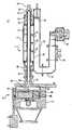
Translated fromKorean도 1은 플라즈마 애셔(plasma asher)에 사용되는 마이크로웨이브 밀폐부의 투시도.1 is a perspective view of a microwave seal used in a plasma asher.
도 2는 본 발명에서 사용하기에 적합한 플라즈마 반응 챔버의 개략 단면도.2 is a schematic cross-sectional view of a plasma reaction chamber suitable for use in the present invention.
도 3은 도 2에 나온 플라즈마 애셔의 투시도.3 is a perspective view of the plasma asher shown in FIG. 2.
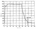
도 4는 CCD계 분광계로 모니터링한 수소 함유 가스를 함유한 무산소 플라즈마에 의한 애싱 공정도중의 387 nm에서 방출된 광강도의 시간경과에 따른 변화를 나타낸 2차원 그래프.Figure 4 is a two-dimensional graph showing the change over time of the light intensity emitted at 387 nm during the ashing process by an oxygen-free plasma containing a hydrogen-containing gas monitored by a CCD-based spectrometer.
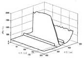
도 5는 도 4에 나온 애싱 공정동안에 200 nm 내지 500 nm에서 방출된 광강도의 시간경과에 따른 변화를 나타낸 3차원 그래프.FIG. 5 is a three-dimensional graph showing the change over time of the light intensity emitted at 200 nm to 500 nm during the ashing process shown in FIG.
도 6은 CCD계 분광계로 모니터링한 플루오르 함유 가스를 함유한 무산소 플라즈마에 의한 애싱 공정 도중의 387 nm에서 방출된 광강도의 시간경과에 따른 변화를 나타낸 2차원 그래프.FIG. 6 is a two-dimensional graph showing changes over time of light intensity emitted at 387 nm during an ashing process by an oxygen-free plasma containing a fluorine-containing gas monitored by a CCD-based spectrometer. FIG.
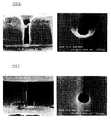
도 7은 본 발명에 의한 무산소 플라즈마 박리 공정 전후에 있어서의 접촉 홀(contact hole)의 단면 및 위에서 본 면을 나타낸 주사전자 현미경 사진.Fig. 7 is a scanning electron micrograph showing a cross section of the contact hole and a plane viewed from above before and after the anaerobic plasma stripping process according to the present invention.
관련출원의 상호참조Cross Reference of Related Applications
본 출원은 1999년 8월 5일자로 출원된 미합중국 특허출원 제09/368,553호(발명의 명칭: 무산소 플라즈마 박리 공정)의 일부 계속 출원으로서, 이를 본 발명에 참고로 원용한다.This application is part of US patent application Ser. No. 09 / 368,553 filed on August 5, 1999, entitled "Anoxic Plasma Stripping Process", which is incorporated herein by reference.
본 발명은 플라즈마 애싱(ashing) 시스템에 관한 것이다. 더욱 상세하게는 본 발명은 기판으로부터 포토레지스트 및/또는 잔류물을 제거하는데 사용되는 무산소 플라즈마 공정의 종점을 검출하는 방법에 관한 것이다. 특히, 무산소 플라즈마는 포토레지스트 및/또는 잔류물과 반응하여 반응 생성물로부터 광학 방출 신호를 발생시키는데, 이 신호를 광학적으로 모니터링하여 애싱 종점을 결정한다.The present invention relates to a plasma ashing system. More particularly, the present invention relates to a method for detecting the end point of an oxygen free plasma process used to remove photoresist and / or residues from a substrate. In particular, the oxygen free plasma reacts with the photoresist and / or residues to generate an optical emission signal from the reaction product, which is optically monitored to determine the ashing endpoint.
애싱은 포토레지스트 및 잔류물을 플라즈마에 노출시켜 반도체 웨이퍼 등으로부터 박리하거나 제거하는 플라즈마 공정이다. 애싱 공정은 일반적으로 에칭, 주입 및 증착 공정이 수행된 이후 실시되는데, 이 경우 포토레지스트 재료가 하부의 기판에 패턴을 에칭하거나 이온을 증착하기 위한 마스크로서 사용된다. 에칭 또는 증착 공정 후 웨이퍼에 잔류하는 포토레지스트 및 잔류물을 제거할 필요가 있다. 보편적으로 애싱 공정에 사용되는 플라즈마는 산소를 한가지 성분으로 함유하는 가스 혼합물로부터 발생되고 있다. 반응성이 큰 유산소 플라즈마(oxygen containing plasma)는 산화반응에 의하여 포토레지스트 및 잔류물을 제거한다. 애싱 동작에 의해 생기는 산화반응 생성물 또는 연소 생성물은 이산화 탄소 및 수증기 등과 같이 보편적으로 휘발성이 있는 성분들이며 가스 유출로 배출된다.Ashing is a plasma process in which photoresist and residues are exposed to plasma to exfoliate or remove from semiconductor wafers or the like. The ashing process is generally carried out after the etching, implanting and deposition processes are performed, in which case the photoresist material is used as a mask for etching patterns or depositing ions on the underlying substrate. It is necessary to remove the photoresist and residues remaining on the wafer after the etching or deposition process. The plasma used in the ashing process is generally generated from a gas mixture containing oxygen as one component. Reactive oxygen containing plasma removes photoresist and residues by oxidation. Oxidation or combustion products produced by the ashing operation are commonly volatile components such as carbon dioxide and water vapor and are discharged to the gas stream.
애싱시에 나타나는 문제점은 포토레지스트 및/또는 잔류물이 제거되는 때를 측정할 때의 정확성이다. 정확한 종점 검출은 고성능 집적 회로의 높은 생산수율에 있어서 극히 중요하다. 일반적으로, 당업자들에게 잘 알려져 있는 여러 가지 이유로 언더에칭(underetching) 또는 오버에칭(overetching)은 바람직하지 않다. 예컨대, 오버에칭은, 패터닝된 회로의 임계적인 치수의 허용오차가 극히 작기 때문에 장치 성능에 영향을 미칠 수 있는 선폭변화를 야기한다.A problem with ashing is the accuracy in measuring when the photoresist and / or residues are removed. Accurate end point detection is critical for the high yield of high performance integrated circuits. In general, underetching or overetching is not desirable for various reasons well known to those skilled in the art. For example, overetching results in linewidth variations that can affect device performance because the tolerances of the critical dimensions of the patterned circuit are extremely small.
포토레지스트 및/또는 잔류물이 제거된 때를 측정하는 한가지 기술은 포토레지스트와 플라즈마 사이의 반응을 그대로 모니터링 하는 것이다. 이 기술은, 광 방출 분광법, 질량 분광법, 레이저 간섭 측정법, 타원 편광법 및 당업자들에게 일반적으로 공지되어 있는 그 밖의 다른 기술과 같은 각종 수단에 의해 달성될 수 있다. 이들 중에서 광방출 분광법은 다른 모니터링 기술에 비교하여 비침투성, 상대적인 경비저렴 및 지속성으로 인하여 가장 바람직하다. 광방출 분광법에 의한 다수의 종점 검출방식은, 플라즈마와 포토레지스트 및/또는 잔류물 사이의 반응에 의해 생긴 방출 신호 및/또는 플라즈마의 화학성분에 의해 결정되는 소정의 스펙트럼선 또는 영역을 모니터링하는 유산소 플라즈마 애싱 공정에 대하여 정의된 것이다. OH 또는 CO 관능기는 포토레지스트 및/또는 잔류물의 유산소 플라즈마 박리 공정중에 생긴 1차 방출 신호가기 때문에 우선적으로 모니터링된다.One technique for measuring when the photoresist and / or residue is removed is to monitor the reaction between the photoresist and the plasma as is. This technique can be accomplished by various means such as light emission spectroscopy, mass spectroscopy, laser interferometry, elliptical polarization, and other techniques generally known to those skilled in the art. Of these, light emission spectroscopy is most preferred due to its non-invasiveness, relative cost savings and persistence compared to other monitoring techniques. Many endpoint detection methods by light emission spectroscopy are aerobic, which monitors a given spectral line or region determined by the emission signal and / or the chemical composition of the plasma resulting from the reaction between the plasma and the photoresist and / or residues. It is defined for the plasma ashing process. OH or CO functionalities are preferentially monitored because they are primary emission signals generated during the aerobic plasma exfoliation process of photoresist and / or residues.
유산소 플라즈마에서 최근 표면화된 문제점은, 이들이 일반적으로 구리 및 가장 낮은 k상호접속을 이용하여 사용하기에 적합하지 않다는 것이다. 구리 및 낮은 k의 재료들은, 디바이스 제작자들이 0.35 φm 디자인 룰을 초과하여 이행해 가기 때문에 여러 가지 이유로 해서 바람직하다. 예컨대, 구리는 알루미늄보다 저항율이 낮으므로 작은 면적에서도 보다 많은 전류를 이동시키기 때문에 증가된 계산능력을 갖는 보다 신속하고 조밀한 집적 회로 등이 가능하다. 더욱이, 낮은 k 유전체 등의 상호접속용의 새로운 절연 재료들은 보다 낮은 상호접속 캐패시턴스와 누화 잡음(crosstalk noise)을 발생시키므로, 회로성능을 향상시킨다. 낮은 k 유전체는, 일반적으로 유전상수가 약 3.5 미만인, 집적 회로 등의 제조에 사용하기에 적합한 재료로서 규정될 수 있다. 이들 낮은 k의 유전체를 광의로 분류하면 4가지 카테고리, 즉 유기, 도핑된 산화물, 다공성 및 테플론(TEFLON) 유사물로 구분할 수 있다. 가장 낮은 k 유전체는 특히 플라즈마 형태로 산소 존재를 허용한다. 상기 카테고리의 다수의 낮은 k 유전체는 포토레지스와 거의 동일한 속도로 에칭되거나, 또는 보다 양호한 에칭 선택도를 나타내지만, 유산소 플라즈마에 노출시키는 동안에 k값이 증가한다는 것이 공지되어 있다. 레지스트 박리 속도를 늦추는데 종종 사용되는 극히 희박한 산소 혼합물을 사용한다 하더라도 다수의 낮은 k값의 재료들에 대한 이러한 문제가 극복되지 않는다.A recent surfaced problem in aerobic plasmas is that they are generally not suitable for use with copper and the lowest k interconnects. Copper and low k materials are desirable for a variety of reasons, as device manufacturers implement more than 0.35 mm design rules. For example, copper has a lower resistivity than aluminum, so that more current can be moved even in a small area, thereby enabling faster and more compact integrated circuits with increased computational power. Moreover, new insulating materials for interconnects, such as low k dielectrics, generate lower interconnect capacitance and crosstalk noise, thus improving circuit performance. Low k dielectrics can be defined as materials suitable for use in the manufacture of integrated circuits and the like, which generally have a dielectric constant of less than about 3.5. These broad k dielectrics can be broadly classified into four categories: organic, doped oxides, porous and TEFLON analogs. The lowest k dielectric allows the presence of oxygen, especially in plasma form. Many low k dielectrics of this category are etched at about the same rate as photoresists, or exhibit better etching selectivity, but it is known that k values increase during exposure to aerobic plasma. Even with the use of extremely sparse oxygen mixtures that are often used to slow the resist stripping rate, this problem for many low k materials is not overcome.
따라서, 무산소 플라즈마를 사용하는 것이 낮은 k의 재료들로부터 포토레지스트 및/또는 잔류물을 제거하는데 효과적이라는 것이 확인되었다. 포토레지스트 박리를 위한 이러한 무산소 플라즈마 공정에 대해서는 1999년 8월 5일자로 출원된 미합중국특허 제09/368,553호(발명의 명칭: 무산소 플라즈마 박리 공정)에 개시되어 있는데, 본 발명에서도 이를 원용하고 있다. 포토레지스트 및/또는 잔류물을 박리하기 위한 무산소 플라즈마를 사용하여 그 종점을 검출하는 광학적인 방법에 대해서는 아직 정의되어 있지 않다. 애싱 종점을 검출하는 기존의 방법들은, 정확한 종점을 검출할 수 있는 원하는 크기를 갖는 신호를 발생시킬 정도로 OH 또는 CO 관능기가 충분히 존재하지 않기 때문에 무산소 플라즈마 사용도중에 종점을 검출하기에는 적합하지 않다.Thus, it has been found that using an oxygen free plasma is effective to remove photoresist and / or residues from low k materials. Such an oxygen-free plasma process for photoresist stripping is disclosed in U.S. Patent No. 09 / 368,553 filed on August 5, 1999, entitled Oxygen-Free Plasma Stripping Process, which is also incorporated herein. The optical method of detecting the end point using an oxygen free plasma for exfoliating photoresist and / or residue is not yet defined. Existing methods of detecting ashing endpoints are not suitable for detecting endpoints during anaerobic plasma use because there are not enough OH or CO functional groups to generate a signal having a desired magnitude capable of detecting the exact endpoint.
따라서, 무산소 플라즈마에 의한 포토레지스트 및/또는 잔류물 제거 공정에서의 애싱 종점 검출 방법을 필요로 하고 있다.Therefore, there is a need for an ashing end point detection method in a photoresist and / or residue removal process using an oxygen free plasma.
본 발명의 목적은 무산소 플라즈마 박리에서의 애싱 종점을 정확히 측정하는 신뢰성 있는 방법을 제공하는 것이다. 본 발명의 방법은 애싱 종점을 정확히 측정함으로써 언더에칭 또는 오버에칭에서 생기는 여러가지 문제를 유리하게 피할 수 있다. 더욱이 본 발명의 방법은, 종래의 OH 또는 CO의 전이를 측정할 때 이미 관찰된 것보다 신호 대(對) 잡음비가 훨씬 더 높은 방출 신호를 가진 파장 또는 파장 범위를 모니터링한다. 이와 같이 애싱 종점은, 한정된 것은 아니나 웨이퍼 가열램프로부터 방출된 복사선 및 플라즈마 자체로부터 방출된 복사선을 포함하는 고유의 잡음계에서 사용될 수 있다.It is an object of the present invention to provide a reliable method for accurately measuring the ashing end point in anoxic plasma stripping. The method of the present invention can advantageously avoid various problems resulting from underetching or overetching by accurately measuring the ashing end point. Moreover, the method of the present invention monitors wavelengths or wavelength ranges with emission signals having a much higher signal-to-noise ratio than previously observed when measuring transitions of conventional OH or CO. As such, the ashing endpoint can be used in a proprietary noise meter that includes, but is not limited to, radiation emitted from a wafer heating lamp and radiation emitted from the plasma itself.
본 발명의 방법은 포토레지스트 및/또는 잔류물을 가진 기판을 반응 챔버속에 설치하는 단계를 포함한다. 수소 함유 가스, 플루오르 함유 가스 및 플루오르-수소 함유 가스 혼합물로부터 선택된 1종과 질소 가스를 함유한 가스 조성물을 여기(exciting)시켜 무산소 플라즈마를 형성한다. 무산소 플라즈마는 표면에 포토레지스트 및/또는 잔류물을 가진 기판과 반응하여, CO 또는 OH 이외의 통상적이지 않은 전이를 갖는 반응 생성물에 상응한 방출된 광신호를 발생시킨다. 반응 생성물로부터 나오는 광방출 강도 신호를 일정시간에 걸쳐 순차적으로 기록한다. 반응 생성물의 광방출 강도 신호가 더 이상 검출되지 않을 때에 종점을 측정한다. 반응에서는, 무엇보다도 약 387 nm의 파장에서의 1차 신호 및 약 358 nm와 약 431 nm에서의 2차 방출 신호에서 방출하는 무산소 라디칼 또는 무산소 화합물을 생성한다.The method includes the step of installing a substrate with photoresist and / or residue in a reaction chamber. A gas composition containing one selected from a hydrogen containing gas, a fluorine containing gas, and a fluorine-hydrogen containing gas mixture and a nitrogen gas is excited to form an oxygen free plasma. The oxygen free plasma reacts with a substrate having photoresist and / or residues on its surface, generating an emitted optical signal corresponding to a reaction product having an unusual transition other than CO or OH. The light emission intensity signal from the reaction product is recorded sequentially over time. The endpoint is measured when the light emission intensity signal of the reaction product is no longer detected. The reaction produces anoxic radicals or anoxic compounds which, among other things, emit in a primary signal at a wavelength of about 387 nm and a secondary emission signal at about 358 nm and about 431 nm.
한가지 실시형태에 있어서, 약 387 nm에서 1차 방출 신호를 포함하는 파장 범위내에서 방출된 광을 CCD계 분광계 등의 분광계를 이용하여 기록한다. 상기 파장 범위에서 약 387 nm에서의 방출 신호의 강도가 그 이상 더 검출되지 않거나 임계값 미만의 정상상태에 도달하면, 적당한 알고리즘을 이용하여 애싱 종점이 측정되고 플라즈마가 차단되어 오버에칭을 방지한다. 바람직하게는 파장 범위는 약 358 nm 및 약 431 nm에서의 2차 방출 신호를 포함한다. 소정의 임계값은 포토레지스트, 잔류물 및 플라즈마 사이의 반응에 의해 생기지 않는 1차 및 2차 파장에서의 방출 신호에 대한 기여를 나타낸다.In one embodiment, light emitted within a wavelength range including the primary emission signal at about 387 nm is recorded using a spectrometer such as a CCD spectrometer. If the intensity of the emission signal at about 387 nm in this wavelength range is no longer detected or reaches a steady state below the threshold, an ashing endpoint is measured using a suitable algorithm and the plasma is blocked to prevent overetching. Preferably the wavelength range comprises a secondary emission signal at about 358 nm and about 431 nm. The predetermined threshold represents the contribution to the emission signal at the primary and secondary wavelengths not caused by the reaction between the photoresist, residue and plasma.
다른 실시형태에서는 약 387 nm의 특정 파장이 모노크로메이터 (monochromator) 등에 의하여 광학적으로 측정된다. 플라즈마를 포트레지스트 및/또는 잔류물과 반응시키기에 앞서, 약 387 nm의 1차 방출 신호에서의 1차 빙츨 강도 신호가 측정된다. 1차 빙츨 강도 신호는 플라즈마 등의 소오스 및 웨이퍼 가열램프로부터의 복사선을 포함하는 백그라운드 복사선을 나타낸다. 바람직하게는 1차 강도신호 측정 동안 블랭크 또는 더미 웨이퍼(blank 또는 dummy wafer)가 이용된다. 표면에 포토레지스트 및/또는 잔류물을 가진 기판을 플라즈마의 반응성 종(reactive species)에 노출시켜 약 387 nm에서 2차 방출 강도 신호를 발생시킨다. 바람직하게는 플라즈마의 반응성 종은 전기적으로 중성이다. 포토레지스트 및/또는 잔류물은 무산소 플라즈마의 반응성 종과 반응하여 통상적이지 않은 휘발성 생성물을 생성하는데, 이들 생성물은 유산소 플라즈마에 노출시키는 동안에 생성된 것들과는 극히 상이하다. 이들 생성물은 약 387 nm에서 1차 광신호를 방출하고, 약 358 nm 및 약 431 nm에서 2차 광신호를 방출한다. 애싱 종점의 검출 방법은, 플라즈마가 기판에 노출될 때 약 387 nm의 1차 광신호에서 2차 방츨 강도 신호를 측정하는 것을 추가로 포함한다. 선택적으로, 2차 광신호를 측정하여 종점을 결정할 수 있다. 플라즈마 박리 공정의 애싱 종점은, 1차 강도신호를 2차 강도신호와 비교하여 상기 1차 및 2차 강도가 거의 동일할 때 종점을 검출함으로써 결정된다. 따라서, 애싱 종점은 반응 생성물이 더 이상 방출되지 않을 때 측정되는 것인데, 이것은 포토레지스트 및/또는 잔류물이 검출가능한 방출 신호를 발생시킬 정도로 충분한 양으로 더 이상 존재하지 않음을 뜻한다.In another embodiment, a specific wavelength of about 387 nm is optically measured by a monochromator or the like. Prior to reacting the plasma with the photoresist and / or residues, the primary bintzing intensity signal at the primary emission signal of about 387 nm is measured. The primary ice intensity signal represents background radiation including radiation from a source such as plasma and a wafer heating lamp. Preferably a blank or dummy wafer is used during the first intensity signal measurement. A substrate having photoresist and / or residues on its surface is exposed to reactive species of the plasma to generate a secondary emission intensity signal at about 387 nm. Preferably the reactive species of the plasma are electrically neutral. The photoresist and / or residues react with reactive species of the oxygen free plasma to produce unusual volatile products, which are extremely different from those produced during exposure to an aerobic plasma. These products emit a primary optical signal at about 387 nm and a secondary optical signal at about 358 nm and about 431 nm. The method of detection of the ashing endpoint further comprises measuring the secondary spectral intensity signal in the primary optical signal of about 387 nm when the plasma is exposed to the substrate. Optionally, the endpoint can be determined by measuring the secondary optical signal. The ashing endpoint of the plasma peeling process is determined by comparing the primary intensity signal with the secondary intensity signal and detecting the endpoint when the primary and secondary intensities are approximately equal. Thus, the ashing endpoint is measured when the reaction product is no longer released, meaning that the photoresist and / or residue is no longer present in an amount sufficient to generate a detectable emission signal.
본 발명은 무산소 플라즈마법에서의 애싱 종점을 결정하는데 사용될 수 있는데, 이 방법에서는 통상적인 CO 및 OH의 전이가 정확한 종점 검출을 위해 원하는 크기의 검출가능한 광신호를 발생시키기에 충분히 존재하지 않는다. 가스 조성물중의 특정성분이, 플라즈마 형성 조건에서의 가스 및 플라즈마 형성 능력 및 낮은 k값의 재료들에 대한 손상 정도가 거의 없는 것 등에 따라 선택된다. 무산소 플라즈마를 발생시키는 가스 조성물은 질소 가스와 반응성 가스를 함유하는 것이 바람직하다. 바람직하게는 반응성 가스는 무산소 플라즈마를 형성하는 수소 함유 가스, 플루오르 함유 가스 및 플루오르-수소 함유 가스 혼합물중에서 선택된 어느 한가지이다. 질소가 반응성 가스, 즉 플루오르 함유 화합물 또는 수소 함유 화합물 중의 어느 한가지와의 혼합물로서 존재하는 경우에 있어서는, 질소가 별도로 공정가스로서 첨가된다. 성분들은 가스로서 플라즈마 애셔(asher)에 조합 및 첨가되는 것이 바람직하다.The present invention can be used to determine the ashing end point in an oxygen free plasma method, where conventional transitions of CO and OH are not sufficiently present to generate a detectable optical signal of the desired size for accurate end point detection. The particular component in the gas composition is selected depending on the gas and plasma forming ability at the plasma forming conditions, the degree of damage to the low k materials, and the like. It is preferable that the gas composition which produces | generates an oxygen free plasma contains nitrogen gas and a reactive gas. Preferably, the reactive gas is any one selected from a hydrogen containing gas, a fluorine containing gas and a fluorine-hydrogen containing gas mixture forming an oxygen free plasma. In the case where nitrogen is present as a mixture with a reactive gas, i.e., a fluorine-containing compound or a hydrogen-containing compound, nitrogen is added separately as a process gas. The components are preferably combined and added to the plasma asher as a gas.
바람직하게는 플라즈마와 포토레지스트 및/또는 잔류물의 반응동안에 방출 신호를 광학적으로 측정하는 방법은 광검출기를 사용한다. 본 발명에서 사용하기에 적합한 장치로서는 모노크로메이터, 분광계 등이 포함된다. 본 발명에서 사용하기에 적합한 기타의 분광분석법은 이러한 점에서 당업자들에게 공지되어 있다. 본 발명은 어떠한 특정의 광방출 분광분석 수단 또는 필터에 한정되는 것은 아니다. 일반적으로 각종 분광계 사이의 차이는 모니터링되는 파장 범위 및 해당하는 방출된 화학종으로부터의 백그라운드 복사선을 구별할 수 있는 구별 능력이다. 여러 가지 분광계 구성등을 이용하여 플라즈마, 포토레지스트 및 잔류물의 반응으로부터 방출된 복사선으로부터 백그라운드 복사선을 구별하는 방법은 이 기술분야에 널리 공지되어 있다.Preferably the method of optically measuring the emission signal during the reaction of the plasma with the photoresist and / or residue uses a photodetector. Suitable devices for use in the present invention include monochromators, spectrometers and the like. Other spectroscopic methods suitable for use in the present invention are known to those skilled in the art in this respect. The invention is not limited to any particular light emission spectroscopic means or filter. In general, the difference between the various spectrometers is the ability to distinguish between the wavelength range monitored and the background radiation from the corresponding emitted species. Methods of distinguishing background radiation from radiation emitted from the reaction of plasma, photoresist and residue using various spectrometer configurations and the like are well known in the art.
본 발명의 여러 가지 목적, 장점 및 특징은 첨부된 도면과 관련하여 기재된 발명의 상세한 설명으로부터 명백히 알 수 있게 된다.Various objects, advantages and features of the present invention will become apparent from the detailed description of the invention described in conjunction with the accompanying drawings.
본 발명은 일반적으로 반도체 웨이퍼 등의 기판으로부터 포토레지스트 및/또는 잔류물을 제거하기 위해 무산소 플라즈마를 사용하는 플라즈마 박리 공정의 종점을 검출하는 방법에 관한 것이다. 무산소 플라즈마는 무산소 공정가스를 여기(勵起)하여, 포토레지스트 및/또는 잔류물과 반응하여 특히 휘발성 부산물을 생성하는 반응성 플라즈마를 생성함으로써 발생된다. 부산물은 유산소 플라즈마에서 관찰된 통상적인 전이, 즉 OH 및 CO와 관련된 전이를 포함하지 않다는데 특징이 있다. 본 발명의 무산소 플라즈마는 무산소 가스중에서 질소가 함유되어야 한다. 질소는 반응성 가스의 혼합물의 일부로서 또는 별도의 공정가스로서 첨가될 수 있다. 한가지 실시형태에 있어서 종점 측정은, 무산소 플라즈마와 포토레지스트 및/또는 에칭후의 잔류물 사이의 반응에서 생긴 약 387 nm에서 1차 광신호를 방출하는 특정의 휘발성 부산물을 포함하는 파장 범위를 모니터링함으로써 이루어진다. 다른 실시형태에 있어서는 종점 측정은 약 387 nm의 특정 파장을 모니터링함으로써 이루어진다. 임의로 약 358 nm 및 431 nm의 파장에서의 2차 방출 신호를 약 387 nm에서 방출된 1차 방출 신호와 함께 모니터링해도 되고 또는 별도로 모니터링해도 된다. 바람직하게는 이들 두가지 실시형태에서의 반응을 모니터링하는 수단은 모노크로메이터 또는 분광계 또는 기타 스펙트럼 모니터 등을 사용하는 광 방출 분광법이다. 일반적으로 모노크로메이터는 스펙트럼의 좁은 부분을 분리하는데 사용되는 반면, 분광계는 넓은 범위의 파장을 측정할 수 있다.The present invention generally relates to a method for detecting the end point of a plasma stripping process using an oxygen free plasma to remove photoresist and / or residues from a substrate such as a semiconductor wafer. An oxygen free plasma is generated by exciting an oxygen free process gas to produce a reactive plasma that reacts with photoresist and / or residues to produce volatile byproducts. By-products are characterized by not including the usual transitions observed in aerobic plasmas, ie those associated with OH and CO. The oxygen free plasma of the present invention should contain nitrogen in the oxygen free gas. Nitrogen may be added as part of the mixture of reactive gases or as a separate process gas. In one embodiment, the endpoint measurement is made by monitoring a wavelength range that includes certain volatile byproducts that emit a primary optical signal at about 387 nm resulting from the reaction between the oxygen free plasma and the photoresist and / or residue after etching. . In another embodiment, endpoint measurement is made by monitoring a particular wavelength of about 387 nm. Optionally, the secondary emission signal at wavelengths of about 358 nm and 431 nm may be monitored with the primary emission signal emitted at about 387 nm or may be monitored separately. Preferably the means for monitoring the reaction in these two embodiments is light emission spectroscopy using a monochromator or spectrometer or other spectral monitor or the like. Monochromators are typically used to separate narrow portions of the spectrum, while spectrometers can measure a wide range of wavelengths.
플라즈마와 포토레지스트 및/또는 잔류물 사이의 반응에서는 무엇보다도 무산소 화합물 또는 무산소 라디칼을 생성하는데, 이들은 약 387 nm의 파장에서 적어도 하나의 검출가능한 1차 광신호와 약 358 nm 및 431 nm의 파장에서 2차 방출 신호를 방출한다. 바람직한 종점 검출 방법은 무엇보다도 약 387 nm의 파장에서의 1차 방출 신호를 포함하는 파장 범위를 분광계 등으로 모니터링하는 단계를 포함한다. 바람직하게는 모니터링된 파장 범위 또는 파장들은 약 358 nm 및 431 nm에서의 2차 방출 신호를 포함한다. 2차 방출 신호는 1차 방출 신호보다 낮은 신호강도를 가지며, 약 387 nm에서 1차 방출 신호를 발생시키는 동일한 반응 부산물에 의해 발생된다고 믿어진다. 애싱 공정의 종점은, 약 358 nm, 387 nm 또는 431 nm에서 기판위의 포토레지스트 및/또는 잔류물과 플라즈마 사이의 반응으로부터 광방출 강도 신호가 더이상 검출되지 않을때 결정된다. 반응으로부터 더 이상 빙츨 강도가 검출되지 않게 되면, 특히 약 387 nm에서의 1차 파장에서 신호가 플라즈마 애셔(asher)의 제어 유닛에 전송되고 애싱 단계의 종료를 나타내게 된다.The reaction between the plasma and the photoresist and / or residues, among other things, produces oxygen-free compounds or oxygen-free radicals, which are at least one detectable primary light signal at a wavelength of about 387 nm and at wavelengths of about 358 nm and 431 nm. Emits a secondary emission signal. Preferred endpoint detection methods include, among other things, monitoring a wavelength range including a primary emission signal at a wavelength of about 387 nm with a spectrometer or the like. Preferably the monitored wavelength range or wavelengths comprise a secondary emission signal at about 358 nm and 431 nm. It is believed that the secondary emission signal has a lower signal intensity than the primary emission signal and is caused by the same reaction byproduct that generates the primary emission signal at about 387 nm. The end point of the ashing process is determined when the light emission intensity signal is no longer detected from the reaction between the plasma and the photoresist and / or residue on the substrate at about 358 nm, 387 nm or 431 nm. Once no more glacial intensity is detected from the reaction, the signal is transmitted to the control unit of the plasma asher, in particular at the primary wavelength at about 387 nm, indicating the end of the ashing step.
소정의 임계값은 일반적으로 약 387 nm에서의 백그라운드 복사선의 양에 의해 결정되거나, 또는 CCD계 분광계를 사용할 경우는 파장 범위에 걸쳐 사용된다. 백그라운드 복사선은, 한정된 것은 아니지만 플라즈마로부터 방출된 복사선, 반응 챔버에서 플라즈마와 불순물 사이의 반응으로 생긴 복사선, 공정중에 웨이퍼를 가열하는데 사용될 수 있는 램프로부터 방출된 복사 에너지 또는 미광을 비롯하여 수많은 소오스에서 발생한다.The predetermined threshold is generally determined by the amount of background radiation at about 387 nm, or used over a wavelength range when using a CCD spectrometer. Background radiation originates from numerous sources, including but not limited to radiation emitted from plasma, radiation resulting from reactions between plasma and impurities in the reaction chamber, radiation energy or stray light emitted from lamps that can be used to heat the wafer during the process. .
모노크로메이터로 형성된 플라즈마 애셔에 있어서, 백그라운드 복사선의 양은 플라즈마 반응기를 통해 블랭크 또는 더미 웨이퍼를 이용하고, 또한 부가적으로 해당하는 방출 신호를 포함하는 파장을 측정함으로써 용이하게 결정될 수 있다. 블랭크 또는 더미 웨이퍼를 사용하여 백그라운드 복사선을 검출하는 것은, 이들을 사용함으로써 얻어지는 조건이 코팅된 웨이퍼 공정중에 사용되는 실제 조건을 나타내기 때문에 바람직하다. 다음으로, 백그라운드 복사선이 임계값을 결정하는데 사용될 수 있으며, 방출 신호가 소정의 임계값에 도달할 때 애싱 종점이 결정된다.For plasma ashers formed with monochromators, the amount of background radiation can be readily determined by using a blank or dummy wafer through the plasma reactor and additionally measuring the wavelengths containing the corresponding emission signals. Detecting background radiation using blanks or dummy wafers is preferred because the conditions obtained by using them represent the actual conditions used during the coated wafer process. Next, background radiation can be used to determine the threshold, and the ashing endpoint is determined when the emission signal reaches a predetermined threshold.
CCD계 분광계 등의 분광계로 형성된 플라즈마 애셔에 있어서, 분광계 시간은, 무산소 플라즈마와 포토레지스트 및/또는 잔류물 사이의 반응으로 생긴 생성물에 상응한 방출 신호를 포함하는 방출 스펙트럼을 순차적으로 기록한다. 바람직하게는 약 387 nm의 파장이 모니터링되는데, 이것은 본 발명에서 해당하는 1차 신호에 상응한 것이다. 약 358 nm 및 약 431 nm의 파장에서의 2차 방출 신호는 1차 방출 신호와 더불어 또는 개별적으로 종점을 측정하는데 사용될 수 있다. 파장 범위에서의 백그라운드 복사선은 애싱 공정도중에 실시간 방출 스펙트럼으로부터 당업자들에게 공지된 방법을 이용하여 제거될 수 있다. 따라서, 모노크로메이터에 대해 앞서 설명한 블랭크 또는 더미 웨이퍼를 이용할 필요가 없어진다. 이와 같이, 약 387 nm에서의 빙츨 강도가 강도 제로(0)에서 정상상태에 도달하면, 애싱 공정의 종점이 검출될 수 있다.In plasma ashers formed with spectrometers such as CCD-based spectrometers, the spectrometer time sequentially records the emission spectra containing emission signals corresponding to products resulting from the reaction between the oxygen free plasma and the photoresist and / or residues. Preferably a wavelength of about 387 nm is monitored, which corresponds to the corresponding primary signal in the present invention. The secondary emission signal at wavelengths of about 358 nm and about 431 nm can be used to determine the endpoint along with or separately from the primary emission signal. Background radiation in the wavelength range can be removed from the real-time emission spectrum during the ashing process using methods known to those skilled in the art. Thus, there is no need to use the blank or dummy wafer described above for the monochromator. As such, when the ice cap intensity at about 387 nm reaches a steady state at zero intensity, the end point of the ashing process can be detected.
무산소 플라즈마 가스의 특정 성분이 플라즈마 형성 조건하에서의 가스 및 플라즈마 형성 능력에 따라 선택되는데, 종종 낮은 k값의 재료들에 대한 손상을 거의 주지않는 정도에 따라 선택되기도 한다. 본 발명에서 사용하기에 적합한 무산소 플라즈마는 무엇보다도 질소를 포함한다. 바람직하게는 성분들이 혼합되어 플라즈마 애셔에 가스 혼합물로서 첨가된다. 무산소 플라즈마 가스는 우선 플라즈마 반응 챔버속에 존재하는 조건하에서 포토레지스트 화합물 및/또는 에칭후의 잔류물내의 탄소 및 기타 원자와 반응하여 휘발성 화합물을 형성한다. 더욱이, 무산소 플라즈마는, 잔류물중에 함유된 실리콘을 통상적으로 함유하는 에칭후의 잔류물을 통상적으로 제거하기 어려운 것들과 반응한다.The particular component of the oxygen free plasma gas is selected according to the gas and the plasma forming ability under plasma forming conditions, often depending on the extent of little damage to low k materials. Oxygen-free plasmas suitable for use in the present invention include, among other things, nitrogen. Preferably the components are mixed and added to the plasma asher as a gas mixture. The oxygen free plasma gas first reacts with the photoresist compound and / or carbon and other atoms in the residue after etching under conditions present in the plasma reaction chamber to form a volatile compound. Furthermore, the oxygen free plasma reacts with those that are typically difficult to remove after etch residues typically containing silicon contained in the residues.
특히 구리와 낮은 k값의 유전체를 사용하는 집적 회로에 사용했을 경우의 바람직한 무산소 플라즈마 가스 조성물은 플루오르 함유 가스, 수소 함유 가스 및 질소 가스의 혼합물이다. 이러한 화합물은 포토레지스트 박리속도의 선택도를, 포토레지스트를 가진 기판과 포토레지스트 층을 노출한 및/또는 그 아래 있는 유전층에서의 유전 에칭 박리속도로 증가시키기에 충분한 반응성 화학종을 생성하는데 매우 유용하다.Particularly when used in integrated circuits using copper and low k dielectrics, the preferred oxygen free plasma gas composition is a mixture of fluorine containing gas, hydrogen containing gas and nitrogen gas. Such compounds are very useful for generating reactive species that are sufficient to increase the selectivity of the photoresist stripping rate to the dielectric etch stripping rate in the dielectric layer that is exposed to and / or below the substrate and photoresist layer having the photoresist. Do.
바람직한 플루오르 함유 화합물은 플라즈마에 의해 여기되었을 때 플루오르 반응성 화학종을 생성하는 화합물들을 포함한다. 바람직하게는 플루오르 함유 가스는 일반식 CxHyFz(여기서 x는 1 내지 4이고, y는 0 내지 9이며, z는 1 내지 10임), NF3, F2, 및 SF6 를 가진 화합물로 구성된 근으로부터 선택된다. 그 밖의 플루오르 함유 화합물들은 본 발명의 개시내용을 고려하면 당업자들에게는 자명한 것이다. 보다 바람직하게는 플루오르 함유 화합물은 CF4또는 CHF3이다.Preferred fluorine containing compounds include those compounds which, when excited by plasma, produce fluorine reactive species. Preferably the fluorine containing gas has the general formula Cx Hy Fz (where x is 1 to 4, y is 0 to 9 and z is 1 to 10), NF3 , F2 , and SF6 Selected from the roots of the compounds. Other fluorine containing compounds will be apparent to those skilled in the art in view of the present disclosure. More preferably the fluorine containing compound is CF4 or CHF3 .
바람직하게는, 플루오르 화합물은 에칭 선택도를 극대화하기 위해 조성물의 총 체적의 약 10% 미만이다. 확인된 바로는, 플루오르 함유 화합물이 약 10 용적% 이상이면 중합이 일어나서 포토레지스트의 제거를 더 어렵게 한다. 더욱이 플루오르 함유 가스를 수소 함유 가스와 병용하면 제거속도가 증가한다는 것을 뜻밖에 발견하였다. 전형적으로 수소 함유 가스를 플루오르 함유 가스와 혼합하면 플루오르화 수소를 생성하게 되는데, 이것은 수소에 의하여 플루오르 라디칼이 제거되기 때문이라고 생각된다. 플라즈마내의 플루오르화 수소는 이산화 실리콘 등의 통상적인 유전체의 제거효율을 저하시킨다는 것으로 공지되어 있다. 따라서 뜻밖에도 낮은 k값의 유전체 존재하에서 잔류물의 제거효율이 증가한다는 것이 관찰되었다.Preferably, the fluorine compound is less than about 10% of the total volume of the composition to maximize etch selectivity. It has been found that if the fluorine-containing compound is at least about 10% by volume, polymerization occurs to make removal of the photoresist more difficult. Furthermore, it was unexpectedly found that the use of fluorine containing gas in combination with hydrogen containing gas increases the removal rate. Typically, mixing a hydrogen containing gas with a fluorine containing gas produces hydrogen fluoride, which is believed to be due to the removal of fluorine radicals by hydrogen. Hydrogen fluoride in plasma is known to reduce the removal efficiency of conventional dielectrics such as silicon dioxide. Thus, it was unexpectedly observed that the removal efficiency of the residues increased in the presence of low k dielectrics.
수소 함유 화합물로서는 수소를 함유한 화합물, 예컨대 탄화수소, 히드로플루오로카본(hydrofluorocarbon), 수소 가스, 수소 가스 혼합물 등을 포함한다. 적당한 수소 가스 혼합물로서는 수소 함유 화합물과 질소의 혼합물, 또는 수소 함유 화합물과 비반응성 가스, 예컨대 아르곤 또는 헬륨과의 혼합물을 포함한다. 사용된 수소 함유 화합물은 박리 공정의 선택도를 증가시키는데 중요한 역할을 한다.Hydrogen-containing compounds include hydrogen-containing compounds such as hydrocarbons, hydrofluorocarbons, hydrogen gas, hydrogen gas mixtures, and the like. Suitable hydrogen gas mixtures include mixtures of hydrogen containing compounds and nitrogen, or mixtures of hydrogen containing compounds with unreactive gases such as argon or helium. The hydrogen containing compounds used play an important role in increasing the selectivity of the stripping process.
바람직한 수소 선구물은, 가스 상태로 존재하고 수소를 방출하여 플라즈마 형성조건하에서 유리 라디칼 또는 수소 이온 등의 반응성 수소종을 형성하는 것들이다. 가스로는, 브롬, 염소 또는 플루오르 등의 할로겐, 또는 산소, 질소, 히드록실 및 아민기와 치환될 수 없거나 또는 부분적으로 치환될 수도 있는 탄화수소가 있다. 바람직하게는 탄화수소는 적어도 하나의 수소와 1 내지 12개의 탄소원자를 가진 것이 좋고, 보다 바람직하게는 3 내지 10개의 탄소원자를 가진 것이 좋다. 수소 함유 가스의 적당한 예로서는 메탄, 에탄, 암모니아 및 프로판을 들 수 있다.Preferred hydrogen precursors are those which are present in gaseous state and release hydrogen to form reactive hydrogen species such as free radicals or hydrogen ions under plasma forming conditions. Gases include halogens such as bromine, chlorine or fluorine or hydrocarbons which may or may not be partially substituted with oxygen, nitrogen, hydroxyl and amine groups. Preferably the hydrocarbon has at least one hydrogen and 1 to 12 carbon atoms, more preferably 3 to 10 carbon atoms. Suitable examples of hydrogen-containing gases include methane, ethane, ammonia and propane.
바람직한 수소 가스 혼합물은 수소 가스와 비활성 가스를 함유한 가스이다. 비활성 가스의 예로서는 아르곤, 질소, 네온, 헬륨 등이 있다. 특히 바람직한 수소 가스 혼합물은 필수적으로 수소 가스와 질소 가스로 된 소위 포밍 가스가다. 본 발명에서 사용하기에 특히 바람직한 것은, 전체 포밍 가스 조성물의 체적에 대해 수소 가스가 약 3 내지 약 5 % 의 양으로 존재하는 포밍 가스인데, 이러한 한정은 플라즈마 애셔 조작시의 안전만을 고려한데서 기인한다.Preferred hydrogen gas mixtures are gases containing hydrogen gas and inert gas. Examples of inert gases include argon, nitrogen, neon, helium and the like. Particularly preferred hydrogen gas mixtures are essentially so-called forming gases consisting of hydrogen gas and nitrogen gas. Particularly preferred for use in the present invention is a forming gas in which hydrogen gas is present in an amount of about 3 to about 5% relative to the volume of the entire forming gas composition, which is due to the safety considerations in plasma asher operation only. .
반응성 가스 혼합물로서 질소가 전혀 존재하지 않을 경우, 즉 플루오르 함유 화합물 또는 수소 함유 화합물인 경우에는 질소를 공정용 가스로 하여 별도로 첨가한다.When nitrogen is not present at all as a reactive gas mixture, that is, in the case of a fluorine-containing compound or a hydrogen-containing compound, nitrogen is added separately as a process gas.
또한, 기타 무산소 플라즈마 가스를 사용하여 플라즈마를 발생시킬 수 있다. 상기한 바와 같이 기타 무산소 플라즈마 가스의 특정 성분은 플라즈마 형성조건하에서 가스와 플라즈마를 형성할 수 있는 능력에 따라 선택되며, 질소를 공정가스중의 1종으로서 또는 혼합물로서 함유한다. 예컨대, 이 가스는 2종 이상의 혼합물이어도 좋고, 또는 각기 별개의 가스이어도 좋다. 본 발명은 특정의 질소를 함유한 무산소 가스 플라즈마에 한정되는 것은 아니다. 특히, 무산소 플라즈마는 포토레지스트 및/또는 잔류물과 반응하여 유산소 플라즈마를 이용하여 전형적으로 생성된 것들과는 상이한 반응 생성물을 생성한다. 약 387 nm에서의 상응하는 1차 방출 신호를 포함한 파장 또는 파장 범위를 모니터링하여 애싱 종점을 측정한다. 본 발명에서 사용하기에 적합한 그 밖의 무산소 가스 플라즈마 조성물은 본 발명의 개시내용을 고려하면 당업자들에게 자명하다.In addition, other oxygen-free plasma gases may be used to generate the plasma. As described above, the specific component of the other oxygen-free plasma gas is selected according to the ability to form the gas and the plasma under plasma forming conditions, and contains nitrogen as one kind of process gas or as a mixture. For example, this gas may be a mixture of two or more kinds, or may be separate gases. The present invention is not limited to oxygen-free gas plasma containing specific nitrogen. In particular, the oxygen free plasma reacts with the photoresist and / or residues to produce different reaction products than those typically produced using an aerobic plasma. The ashing endpoint is determined by monitoring the wavelength or wavelength range including the corresponding primary emission signal at about 387 nm. Other oxygen free gas plasma compositions suitable for use in the present invention will be apparent to those skilled in the art in view of the present disclosure.
종점 검출 방법은 플라즈마 공정 변수와는 관계없이 동일하게 유지된다. 그러나 제거속도는 또한 당업자들에게 공지되어 있는 바와 같이 더욱 최적화될 수 있다. 예컨대 플라즈마 챔버 압력을 약 0.5 torr로부터 약 10 torr까지 변화시킬 수 있고, 전력을 약 500 W로부터 약 2000 W까지 조정할 수 있으며, 웨이퍼를 약 80℃에서부터 약 350℃까지 단계적으로 가열할 수 있고, 또는 총 가스 유속을 약 500 scccm으로부터 약 9000 scccm까지 조정할 수 있다. 이들 조건하에서 발생시킨 무산소 플라즈마는 포토레지스트 및/또는 잔류물과 반응하여 358 nm, 387 nm 및 431 nm에서 방출 신호를 발생하는데, 그 후 이들이 개별적으로 또는 병합하여 모니터링됨으로써 애싱 단계의 종점이 결정된다. 바람직하게는 약 387 nm에서의 1차 방출 신호를 모니터링하여 애싱 종점을 결정한다.The endpoint detection method remains the same regardless of the plasma process parameters. However, the removal rate can also be further optimized as is known to those skilled in the art. For example, the plasma chamber pressure may be varied from about 0.5 torr to about 10 torr, the power may be adjusted from about 500 W to about 2000 W, and the wafer may be heated in steps from about 80 ° C. to about 350 ° C., or The total gas flow rate can be adjusted from about 500 scccm to about 9000 scccm. Oxygen-free plasmas generated under these conditions react with photoresists and / or residues to generate emission signals at 358 nm, 387 nm and 431 nm, which are then monitored individually or in combination to determine the end of the ashing step. . Preferably, the ashing endpoint is determined by monitoring the primary emission signal at about 387 nm.
포토레지스트는 일반적으로 화상을 아래의 기판으로 전사하는데 사용되는 유기 감광성 필름이다. 본 발명은 일반적으로 g선, i선, DUV, 193 nm 및 157 nm 응용에 사용되는 포토레지스트를 박리하는데 적용 가능하다. 이것은 노볼락, 폴리비닐페놀, 아크릴레이트, 아세탈, 케탈, 환상 올레핀 등을 포함하지만, 이에 국한되는 것은 아니다. 그 밖의 적합한 포토레지스트 배합물은 본 발명의 개시 내용을 고려하면 당업자들에게 자명할 것이다. 포토레지스트는 선택된 포토레지스트 화학 및 현상제에 따라 양화용일 수도 있고 또는 음화용일 수도 있다.Photoresists are generally organic photosensitive films used to transfer images to underlying substrates. The present invention is generally applicable to stripping photoresists used in g-ray, i-ray, DUV, 193 nm and 157 nm applications. This includes, but is not limited to, novolacs, polyvinylphenols, acrylates, acetals, ketals, cyclic olefins, and the like. Other suitable photoresist formulations will be apparent to those skilled in the art in view of the present disclosure. The photoresist may be positive or negative, depending on the selected photoresist chemistry and developer.
에칭후 및 증착후의 잔류물은 초기 공정 단계동안 화학적인 변화를 받아 보편적으로 박리 플라즈마에 대해 더 강한 저항성을 갖는 포토레지스트인 것이라 생각된다. 에칭후 잔류물로는 측벽의 폴리머 부착물로서 알려진 잔류물을 포함한다. 초기의 유전 에칭 단계의 결과로서 화학변화가 일어나서, 이로 인해 플라즈마 반응기 라이닝 또는 웨이퍼의 성분이 포토레지스트와 반응하여 에칭후 잔류물을 형성하거나, 플라즈마 공정도중에 생긴 화학종의 반응에서 화학변화가 일어나는 것이라 생각된다.Post-etch and post-deposition residues are believed to be photoresists that undergo chemical changes during the initial process steps and are generally more resistant to delamination plasma. Post-etch residues include residues known as polymer deposits on the sidewalls. Chemical changes occur as a result of the initial dielectric etch step, which causes the plasma reactor lining or the components of the wafer to react with the photoresist to form residues after etching, or to cause chemical changes in the reaction of chemical species during the plasma process. I think.
일반적으로 질소 존재하에서 무산소 플라즈마를 발생시켜 형성된 반응성 화학종은 유산소 플라즈마에서 보편적으로 형성되는 반응 생성물과는 상이하다. 플라즈마 가스 혼합물이 포트레지스트 및/또는 잔류물을 제거하여 생긴 반응성 화학종은 휘발성 생성물을 형성하도록 반응한다. 플라즈마를 사용하는 그 밖의 잔류물 제거방법은 기판에 대한 접착력을 약화시키거나 잔류물을 수용성으로 하는 것이다. 그 후, 잔류물은 탈이온수 세척 단계에서 제거된다. 포토레지스트 및/또는 잔류물들 사이의 반응에서 생기는 휘발성 반응 생성물이 더 이상생기지 않을 때까지 박리 공정을 계속한다. 본 발명에서의 해당 반응 부산물은 약 387 nm에서의 1차 광신호를 방출하는 것이다. 또한, 약 358 nm 및 약 431 nm에서의 2차 방출 신호는 약 387 nm에서의 방출 신호와 병용하거나, 또는 약 387 nm에서의 방출 신호와 독립적으로 사용되어 애싱 종점을 결정할 수 있다.In general, reactive species formed by generating an oxygen free plasma in the presence of nitrogen are different from reaction products commonly formed in aerobic plasmas. The reactive species resulting from the plasma gas mixture removing the photoresist and / or residues react to form volatile products. Other residue removal methods using plasma are to weaken the adhesion to the substrate or to make the residue water soluble. The residue is then removed in a deionized water washing step. The exfoliation process is continued until the volatile reaction product resulting from the reaction between the photoresist and / or residues no longer forms. The corresponding reaction byproduct in the present invention is to emit a primary optical signal at about 387 nm. Further, the secondary emission signal at about 358 nm and about 431 nm can be used in combination with the emission signal at about 387 nm, or used independently of the emission signal at about 387 nm to determine the ashing endpoint.
본 발명에서 사용하기에 특히 적합한 플라즈마 애셔는 하향식 플라즈마 애셔인데, 예컨대 Eaton사에서 GEMINI ES라는 상품명으로 판매되고 있는 마이크로웨이브식 플라즈마 애셔를 들 수 있다. 마이크로웨이브식 플라즈마 애셔에 대해서는 본 발명에서 원용하고 있는 미합중국 특허 제5,498,308호 및 제4,341,592호와 PCT 출원 제WO/97/37055호에 기재되어 있다. 본 발명은 상기 실시예 또는 이하의 실시예에서 어떠한 특정 플라즈마 애셔에 한정되는 것은 아니다. 예컨대 유도결합 플라즈마 반응기를 사용할 수 있다.Particularly suitable plasma ashers for use in the present invention are top-down plasma ashers, such as microwave plasma ashers sold under the trade name GEMINI ES by Eaton. Microwave plasma ashers are described in US Pat. Nos. 5,498,308 and 4,341,592 and PCT Application WO / 97/37055, which are incorporated herein by reference. The invention is not limited to any particular plasma asher in the above embodiments or below. For example, an inductively coupled plasma reactor can be used.
특히, 도 1 및 도 2를 참조하면, 참조번호 10으로 나타낸 마이크로웨이브식 플라즈마 애셔는 무산소 플라즈마 처리에 의한 포토레지스트 및/또는 잔류물 제거방법을 실시할 때 적합하다. 도시된 플라즈마 애셔는 플라즈마 발생 챔버(11) 및 플라즈마 반응 챔버(12)를 포함한다. 플라즈마 발생 챔버는 마이크로웨이브 밀폐부(14)를 가진다. 이 마이크로웨이브 밀폐부는, 플라즈마 튜브(22)가 관통하는 세로방향 구획(16,18,20)으로 분할된 직사각형 상자형이다. 각 구획 마다 플라즈마 튜브가 관통하는 구멍을 가지고 있다. 각 구획에는 마이크로웨이브 에너지가 공급된다. 따라서 각 구획은 유입하는 마이크로웨이브 에너지에 대한 비교적 짧은 공동(cavity)을 가지고 있어서 방위 및 축방향의 균일성을 가진 모드를 형성하도록 한다. 바깥쪽의 튜브(24)는 공동내에서 플라즈마 튜브를 둘러싸고 있다. 바깥쪽의 튜브는 플라즈마 튜브와는 약간 떨어져 있고, 이들 두개의 튜브 사이에 양압(positive pressure)의 공기가 공급되어 플라즈마 튜브를 효과적으로 냉각한다. 튜브(24)는 사파이어로 된 것이 바람직하다. 석영, 알루미나 또는 알루미나 피복 석영 등의 다른 플라즈마 튜브가 사용될 수 있다.In particular, with reference to FIGS. 1 and 2, the microwave plasma asher, indicated by
동심의 튜브가 삽입되는 구획(16,18,20)내의 구멍은 플라즈마 튜브의 외부치수보다 크게 제작된다. 이들 구멍을 통해 마이크로웨이브가 투과하게 되면 튜브속에서 플라즈마를 균일하게 여기(exciting)시키게 된다. 이렇게 투과함으로써, 플라즈마 튜브내에서의 열 기울기(thermal gradient)를 감소시킨다. 바깥쪽의 튜브를 사용하지 않으면(기타의 방식으로 제공되는 냉각), 구획내의 구멍의 크기를, 플라즈마 튜브와 구획 사이에 마이크로웨이브가 투과 할 수 있는 공간을 형성할 수 있는 정도로 한다. 도 1은 바깥쪽의 튜브와 구획 사이의 공간을 나타내고 있다.The holes in the
또한, 도시된 아이리스판(iris plate)(26)은 마이크로웨이브 구조의 개방쪽을 피복하는 것으로서 마이크로웨이브 에너지를 인접한 부분에다 효과적으로 공급한다. 이 판(26)은 마이크로웨이브 에너지가 통과하는 아이리스(28,30,32,34)를 가진 금속제 평판이다.In addition, the illustrated
마이크로웨이브 트랩(36,38)이 양단에 설치되어 있어서 마이크로웨이브의 투과를 방지한다. 이들 트랩은 본원에서 원용한 미합중국 특허 제5,498,308호에 개시된 유형의 것이어도 좋다. 냉각용 공기를 유입시키고 이것을 동심 튜브 사이의 공간에 공급하기 위해 에어 시일(air seal)/지향성 피이더(directional feeder)(40,42)가 제공된다. 에어 시일/지향성 피이더(44)는 바깥쪽 단부에에 도시되어 있으며, 4번째의 피이더도 존재하지만 도시되어 있지 않다.Microwave traps 36 and 38 are provided at both ends to prevent microwave penetration. These traps may be of the type disclosed in US Pat. No. 5,498,308, which is incorporated herein. An air seal /
마그네트론(magnetron)(46)은 커플러(48)를 통해 공급된 마이크로웨이브 전력을 서로 수직관계에 있는 부분(50,52)을 가진 도파관(waveguide) 공급 TE10 모드에 공급한다. 도파관부(52)의 길이는 이동식 플런저(54)에 의하여 조절가능하다. 도파관부(52)의 바닥판은 아리리스판(56)인데, 이것은 마이크로웨이브 에너지를 분할된 마이크로웨이브 구조(14)에 결합하며, 이를 통해 플라즈마 튜브(22)가 연장함으로써; 플라즈마가 플라즈파 튜브를 통해 흐르는 가스내에서 여기된다.The
도 2를 참조하면, 엔드 캡(end cap)(60)이 마이크로웨이브 트랩(38)과 접하며, 가스를 플라즈마 튜브에 유입하는 중심 오리피스를 가진 피팅(fitting)(64)이 이 엔드 캡으로 연장한다는 것을 알 수 있다. 가스공급은 외부 유속조절 박스(도면에 도시없음)에 의하여 조절된다.Referring to FIG. 2, an
플라즈마 튜브를 엔드 캡에서 그 한쪽에다 Ao
바람직하게는 마이크로웨이브 밀폐부(14)의 치수를 직사각형상의 TE110 모우드를 지지할 수 있도록 하고, 이 마이크로웨이브 밀폐부(14)는 정사각형 단면을 가질 수 있다. 이들 단면의 치수는 TE110 모우드가 공진방식이 되도록 한다. 각 단면의 길이는 λg/2(여기서 λg는 TE104 모우드의 공동내에서의 도파관의 길이) 미만이다.Preferably, the dimensions of the
플라즈마 반응 챔버(12)는 처리될 웨이퍼(88)를 지지하는 지지핀(80,82)을 포함한다. 선택적으로, 척(chuck)(도시되지 않음)을 사용해도 좋다. 웨이퍼 아래에 위치한 텅스텐 할로겐 램프(도시되지 않음)를 사용하여 가열이 이루어질 수 있다. 기판은 애싱 처리도중 약 80℃ 에서 약 350℃로 가열되는 것이 바람직하다. 보다 바람직하게는 온도를 점진적으로 올리면서 기판을 단계적으로 가열한다. 가열은 플라즈마와 포토레지스트 및/또는 잔류물과의 반응 속도를 증가시키므로, 결국에는 처리량을 증가시키는 것으로 확인되었다. 웨이퍼 위에 하나 이상의 배플판(baffle plate)(도시되지 않음)을 설치하여 웨이퍼 표면에 대한 플라즈마의 균일한 분포를 도모해도 좋다.The
반응 챔버의 측벽은 석영 또는 사파이어 등의 투명한 재료로 된 광학 포트 구멍(90)을 포함한다. 이 구멍은 웨이퍼면에 거의 평행한 광학 통로를 형성할 수 있도록 구성되고 위치한다. 무산소 플라즈마의 방출 스펙트럼은 이 구멍을 통과한다. 수집 렌즈(도시되지 않음)가 창의 바깥 및 뒤에 설치되어 통과한 방출 스펙트럼을 수집한다. 또한, 분광계 또는 모노크로메이터(도 3에서 일반적으로 92로 나타냄)를 설치하여 수집 렌즈로부터의 광을 수집한다. 광 방출 분광분석 장치 및 기술은 수많은 간행물에 널리 공지되어 있고 언급되어 있다. 한가지 실시형태에 있어서 광 방출 분광분석은 CCD(charge couple device)계 분광계와 같은 분광계에 의해 이루어지며, 시간이 순차적으로 파장 범위를 기록하고 방출 스펙트럼을 아날로그 신호로 변환하여 분석을 한다. 임의로 CCD 또는 광다이오드 어레이와 같은 광검출기상의 해당 파장의 특정 범위을 평가하기 위해 협대역 필터가 사용될 수 있다. 분광계 시간은 애싱 공정동안에 방출된 광신호를 순차적으로 전기적인 아날로그 신호로 변환한 후에 이것을 공지의 방법으로 분석하여 원하는 출력을 생성한다. 바람직하게는 데이터를 실시간으로 표시하는 것이다. 바람직하게는 데이터를 해당하는 파장 범위에 대한 플라즈마 공정 동안 방출된 광강도를 시간경과로 나타내는 그래프 형태로 나타내는 것이다.The side wall of the reaction chamber includes an
또한, 기타의 광검출기가 사용될 수 있다. 예컨대 상기 논의한 바와 같이, 모노크로메이터를 사용하여 데이터를 수집할 수 있다. 공지되어 있는 바와 같이 모노크로메이터는 광전자 증배관, 광전 다이오드 등을 구성하여 약 387 nm에서의 좁은 스펙트럼의 방출 신호를 기록한다.In addition, other photodetectors may be used. For example, as discussed above, monochromators can be used to collect data. As is known, monochromators make up photomultipliers, photodiodes and the like to record a narrow spectrum of emission signals at about 387 nm.
플라즈마 반응 챔버내에서의 적당한 구성 및 상기 광방출 분광분석 장치는 본 발명의 개시 내용을 고려하면 당업자들에게 자명할 것이다. 본 발명에서 사용하기에 적합한 모노크로메이터의 예로서는 미합중국의 Verity사에서 시판하고 있는 모델 No. EP200MMD가 있다. 본 발명에서 사용하기에 적합한 주사식(scanning) 모노크로메이터의 예로서는 미합중국의 Verity사에서 시판하고 있는 모델 No. EP200SMD가 있다. 본 발명에서 사용하기에 적합한 CCD계 분광계의 예로서는 미합중국의 Verity사에서 시판하고 있는 모델 No. SD1024 및 미합중국의 Ocean Optics사에서 시판하고 있는 PC2000 CCD 시리즈 분광계가 있다. 본 발명에서 사용하기에 적합한 광검출기 어레이의 예로서는 독일국의 Prema사에서 시판하고 있는 모델 No. SPM9001이 있다. 무산소 플라즈마 공정에 대한 종점 검출 방법은 약 387 nm에서의 방출된 강도 신호의 변화를 모니터링할 수 있는 능력을 필요로 한다. 임의로, 상기 논의한 바와 같이 약 387 nm에서의 반응 부산물에 상응하여 약 358 nm 및 약 431 nm에서의 2차 파장을 병합하여 모니터링하거나 개별적으로 모니터링할 수 있다.Appropriate configurations within the plasma reaction chamber and the light emission spectroscopy apparatus will be apparent to those skilled in the art in view of the present disclosure. Examples of monochromators suitable for use in the present invention include Model No., commercially available from Verity of the United States. EP200MMD. Examples of scanning monochromators suitable for use in the present invention include Model No., commercially available from Verity of the United States. There is an EP200SMD. As an example of a CCD spectrometer suitable for use in the present invention, Model No. There is a PC2000 CCD series spectrometer available commercially from SD1024 and Ocean Optics of the United States. Examples of photodetector arrays suitable for use in the present invention include Model No., commercially available from Prema of Germany. There is SPM9001. Endpoint detection methods for an oxygen free plasma process require the ability to monitor changes in the emitted intensity signal at about 387 nm. Optionally, as discussed above, secondary wavelengths at about 358 nm and about 431 nm can be combined or monitored separately, corresponding to reaction byproducts at about 387 nm.
도 3에는 장치의 투시도가 도시되어 있다. 도 3에서의 각 참조번호는 기타의 도면에서의 것들과 각각 대응한다.3 is a perspective view of the device. Each reference numeral in FIG. 3 corresponds to those in the other figures, respectively.
조작시, 표면에 포토레지스트 및/또는 에칭후의 잔류물을 가진 반도체 웨이퍼(88)가 반응 챔버(12)속에 웨이퍼 지지핀(80,82) 위에 설치한다. 이 웨이퍼는 포토레지스트 및/또는 에칭후의 잔류물과 플라즈마와의 반응을 촉진시키기 위해 가열되는 것이 바람직하다. 반응 챔버내의 압력은 감소된다. 바람직하게는 압력은 약 1 torr 내지 약 5 torr 사이로 유지된다. 질소를 한가지 성분으로 함유하는 여기성(excitable) 무산소 가스가 가스 유입구(13)(도 3)를 통해 플라즈마 발생 챔버(11)속의 플라즈마 튜브(22)속으로 공급된다. 각 구획(16,18,20)에는 마이크로웨이브 에너지가 공급되어 플라즈마 튜브에서 플라즈마를 여시시키며, 상기 플라즈마는 전기적으로 중성의 대전입자로 구성된다. 대전 입자는 플라즈마가 반응 챔버에 들어가기 전에 선택적으로 제거된다. 가스의 여기된 또는 활성화된 원자가 반응 챔버속으로 공급되어 포토레지스트 및/또는 에칭후의 잔류물과 반응한다. 무산소 플라즈마는 포토레지스트 및/또는 에칭후의 잔류물과 반응하여 휘발성 생성물을 형성한다. 특정의 반응 생성물은 분광계, 모노크로메이터 등의 광방출 분광분석 수단(92)에 의하여 광학적으로 모니터링된다. 휘발성 가스는 렌즈 포트(90)에 의해 전달되도록 반응 챔버내에서 가스 스위프(sweep)에 의해 웨이퍼 표면으로부터 연속해서 스위핑된다.In operation, a
CCD계 분광계로 구성된 플라즈마 애셔에 있어서, CCD계 분광계 시간은 방출되는 약 387 nm에 상응하는 방출 신호를 발생되는대로 포함하는 방출 스펙트럼을 순차적으로 기록한다. 모니터링된 방출 스펙트럼의 파장 범위는 사용되는 CCD계 분광계의 유형 및 소정의 파장 방출이 CCD계 분광계에 도달하지 못하게 하는데 사용되는 임의의 필터의 존재에 의해 결정된다. CCD계 분광계는 애싱 공정동안에 방출된 화학종으로부터 방출되는 복사선 및 백그라운드 복사선을 동시에 기록한다. 공지된 표준 알고리즘을 사용하면, 플라즈마와 포토레지스트 및/또는 잔류물과의 반응에서 생긴 복사선으로부터 백그라운드 복사선을 뺀다. 방출 피이크가 강도값의 변화를 기록하고 최소의 소정 레벨에서의 정상상태에 도달하면, 포토레지스트 및/또는 잔류물의 제거가 완료되고, 이어서 신호가 제어 유닛(94)으로 전송되어 플라즈마가 차단된다. 진공상태가 해제되고, 공정 웨이퍼가 반응 챔버로부터 제거될 수 있다. 박리된 웨이퍼 위에 잔존하는 잔류물을 제거하기 위해 임의의 탈이온수 세척이 사용된다.In a plasma asher consisting of a CCD-based spectrometer, the CCD-based spectrometer time sequentially records the emission spectra containing the emission signals corresponding to the emission of about 387 nm as generated. The wavelength range of the monitored emission spectrum is determined by the type of CCD-based spectrometer used and the presence of any filter used to prevent a given wavelength emission from reaching the CCD-based spectrometer. The CCD-based spectrometer simultaneously records the radiation emitted from the species released during the ashing process and the background radiation. Using known standard algorithms, the background radiation is subtracted from the radiation resulting from the reaction of the plasma with the photoresist and / or residue. When the emission peak records the change in intensity value and reaches a steady state at the minimum predetermined level, removal of the photoresist and / or residue is completed, and then a signal is sent to the
모노크로메이터를 구비한 플라즈마 애셔에 있어서, 코팅되지 않은 블랭크 웨이퍼가 먼저 반응 챔버속에서 노출되고, 약 387 nm에서의 1차 방출 신호가 측정된다. 1차 방출 신호는 상기 논의된 바와 같은 백그라운드 복사선을 나타낸다. 그 다음, 표면에 포토레지스트 및/또는 잔류물을 가진 기판이 반응 챔버내에서 무산소 플라즈마에 노출된다. 약 387 nm에서 방출된 2차 방출 신호가 모노크로메이터에 의해 기록된다. 1차 방출 신호의 백그라운드 복사선을 2차 방출 신호로부터 뺀다. 약 387 nm에서의 2차 방출 신호가 정상상태에 도달하여 1차 방출 신호와 거의 동일하거나 그 이하이면, 애싱 종점에 도달한 것이 되어, 신호가 플라즈마 애셔내의 제어 유닛(94)으로 전송되어 플라즈마가 차단된다. 다음으로, 진공상태가 해제되고, 공정 웨이퍼가 반응 챔버로부터 제거된다. 그 다음, 박리된 웨이퍼위에 잔존하는 잔류물을 제거하기 위해 임의의 탈이온수 세척이 사용된다.In plasma ashers with monochromators, the uncoated blank wafer is first exposed in the reaction chamber and the first emission signal at about 387 nm is measured. The primary emission signal represents background radiation as discussed above. Subsequently, a substrate having photoresist and / or residues on its surface is exposed to an oxygen free plasma in the reaction chamber. The secondary emission signal emitted at about 387 nm is recorded by the monochromator. The background radiation of the primary emission signal is subtracted from the secondary emission signal. If the secondary emission signal at about 387 nm reaches a steady state and is approximately equal to or less than the primary emission signal, the ashing end point has been reached, and the signal is transmitted to the
약 358 nm, 387 nm 및 431 nm의 1차 및 2차 방출 신호에서 반응 부산물을 모니터링하는 기타의 모노크로메이터, 분광계 등의 구성 및 동작은 본 발명의 개시를 고려하면 당업자들에게 자명할 것이다.The construction and operation of other monochromators, spectrometers and the like for monitoring reaction byproducts in primary and secondary emission signals of about 358 nm, 387 nm and 431 nm will be apparent to those skilled in the art in view of the present disclosure.
아래의 각 실시예에서 무산소 플라즈마를 사용하여 포토레지스트를 제거하는 동안에 애싱 종점을 검출하는 방법을 상세히 설명한다. 구체적인 방법은 상기한 방법의 범위에 속하고 그것을 예시하는 것이다. 각 실시예는 설명을 하기 위한 것일 뿐이고 본 발명의 범위를 한정하는 것은 아니다. 예컨대 플라즈마 애셔를 기타의 분광계 또는 모노크로메이터와 더불어 구성하여 약 387 nm에서의 1차 방출 신호를 포함한 방출 신호를 모니터링할 수 있다.In each of the examples below, a method of detecting the ashing end point during the removal of the photoresist using an oxygen free plasma will be described in detail. The specific method belongs to the range of the above-mentioned method, and illustrates it. Each embodiment is for illustrative purposes only and does not limit the scope of the invention. For example, a plasma asher can be configured with other spectrometers or monochromators to monitor the emission signal, including the primary emission signal at about 387 nm.
실시예 1Example 1
아래의 실시예에서, DUV 포토레지스트가 다중 실리콘 웨이퍼에 3000 rpm에서 코팅된다. 포토레지스트는 Shipley사에서 시판하고 있는 상품명 UV6-1.0의 것이다. 각 웨이퍼를 진공 핫플레이트(hotplate)위에서 130℃에서 45초 동안 가열처리한 후, 두께가 약 10,000 Å인 무점착성의 포토레지스트 필름이 얻어진다. 그 다음, 이 포토레지스트 필름은, CCD계 분광계를 포함하도록 구성된 반응 챔버를 이용하여 Eaton사제의 Fusion Gemini ES Plasma Asher를 사용하여 마이크로웨이브 플라즈마에 노출된다. 플라즈마 챔버의 전력은 3.0 torr의 챔버 압력을 가지고 1800W로 설정된다. 웨이퍼는 가스유속 2500 sccm의 포밍 가스로부터 발생된 플라즈마에 노출된다. 사용된 포밍 가스는, 전체 포밍 가스 혼합물에 대해 수소 가스가 3 용적%인 수소 및 질소 가스의 혼합물이다. 웨이퍼가 300℃의 온도까지 가열된다. 플라즈마와 포토레지스트 사이의 반응도중에 방출된 광이, 웨이퍼 표면과 거의 평행한 광통로를 형성하는 반응 챔버의 측벽에서의 창 뒤에 구성된 CCD계 분광계에 의하여 수집된다. 파장 200 및 500 nm 사이의 스펙트럼이 CCD 분광계로 기록되는데, 상기 CCD 분광계는 플라즈마 처리공정의 1초마다 50 ms 동안 방출 신호를 수집한다.In the examples below, the DUV photoresist is coated at 3000 rpm on multiple silicon wafers. The photoresist is a trade name UV6-1.0 sold by Shipley. After each wafer was heat treated at 130 ° C. for 45 seconds on a vacuum hotplate, a tacky photoresist film having a thickness of about 10,000 mm 3 was obtained. This photoresist film is then exposed to microwave plasma using a Fusion Gemini ES Plasma Asher from Eaton using a reaction chamber configured to include a CCD-based spectrometer. The power of the plasma chamber is set to 1800W with a chamber pressure of 3.0 torr. The wafer is exposed to a plasma generated from a forming gas with a gas flow rate of 2500 sccm. The forming gas used is a mixture of hydrogen and nitrogen gas with 3 vol% hydrogen gas relative to the total forming gas mixture. The wafer is heated to a temperature of 300 ° C. Light emitted during the reaction between the plasma and the photoresist is collected by a CCD-based spectrometer configured behind a window at the sidewall of the reaction chamber that forms an optical path that is substantially parallel to the wafer surface. Spectra between
도 4 및 도 5는 무산소 플라즈마에 의한 애싱 처리동안에 200 nm 내지 500 nm에서 방출된 광강도의 시간경과에 따른 상황을 도시하는 그래프이다. 도 4에 도시된 데이터가 CCD계 분광계를 이용하여 수집된 것이라 하더라도, 도 4는 백그라운드 복사선 감산없이 모노크로메이터로 구성된 플라즈마 애셔를 사용하여 얻어진 데이터 유형의 예이다. 약 387 nm에서 현저한 신호가 관찰되고 있다. 이 데이터로부터 애싱 종점은 약 t = 155에서 발생함을 알 수 있다. 즉, 애싱 처리 155초 후에, 플라즈마와 포토레지스트 및/또는 에칭후의 잔류물 사이의 반응이 완료되었다. 155초 후에는 어떠한 검출가능한 방출이 전혀 기록되지 않고 있어, 오버에칭을 방지하기 위해 플라즈마가 차단된다. 이 실시예에서의 데이터로부터, 387 nm에서의 임계값이 250 강도의 방출단위로 설정될 수 있음을 알 수 있다. 실제 생산환경하에서는 유사한 조건을 사용하여 약 387 nm에서의 빙츨 강도가 임계값 미만의 정상상태에 일단 도달하면, 신호가 제어 유닛으로 전송되어 플라즈마를 차단시킨다. 따라서, 애싱 처리 종점이 정확히 결정할 수가 있다. 도 5는 파장이 약 400 nm로부터 500 nm까지 증가함에 따른 빙츨 강도의 점진적인 증가를 나타낸 것인데, 이것은 공정도중 웨이퍼를 가열하는데 사용된 램프에 의하여 발생된 넓은 대역의 복사선에 의해 주로 나타나고 있다. 또한, 도 5는 약 358 nm 및 431 nm에서 2차 신호를 나타낸다.4 and 5 are graphs showing the situation over time of light intensity emitted from 200 nm to 500 nm during ashing treatment with an oxygen free plasma. Although the data shown in FIG. 4 was collected using a CCD spectrometer, FIG. 4 is an example of the type of data obtained using a plasma asher composed of a monochromator without background radiation subtraction. At about 387 nm, a remarkable signal is observed. From this data it can be seen that the ashing endpoint occurs at about t = 155. That is, after 155 seconds of ashing treatment, the reaction between the plasma and the photoresist and / or residue after etching is complete. After 155 seconds no detectable emission is recorded at all, so the plasma is blocked to prevent overetching. From the data in this example, it can be seen that the threshold at 387 nm can be set in emission units of 250 intensity. Under actual production conditions, using similar conditions, once the ice intensity at about 387 nm reaches a steady state below the threshold, a signal is sent to the control unit to block the plasma. Thus, the ashing end point can be determined accurately. FIG. 5 shows a gradual increase in ice intensity as the wavelength increases from about 400 nm to 500 nm, mainly due to the wide band of radiation generated by the lamp used to heat the wafer during the process. 5 also shows the secondary signal at about 358 nm and 431 nm.
실시예 2Example 2
이 실시예에서는, 다중 실리콘 웨이퍼가 박층의 바닥 무반사층으로 코팅된 다음 5000 Å의 포토레지스트로 코팅되어, 플루오르 함유 가스와 질소 가스를 함유한 공정가스로부터 발생된 무산소 플라즈마에 상기 실시예 1과 동일한 조건하에 노출된다. 플루오르 함유 가스는 CF4이다.In this embodiment, multiple silicon wafers were coated with a thin bottom anti-reflective layer and then coated with 5000 kW photoresist, the same as in Example 1 above for anoxic plasma generated from a process gas containing fluorine containing gas and nitrogen gas. Are exposed under conditions. The fluorine containing gas is CF4 .
도 6은 플라즈마 공정중에 측정된 약 387 nm의 파장에서 모니터링한 시간의 함수로서의 빙츨 강도를 도시하는 그래프이다. 종점은 약 42초에서 나타나는데, 이것은 포토레지스트가 제거되고, 오버에칭을 방지하기 위해 플라즈마가 차단되어야 한다는 것을 나타내는 것이다. 각 실시예에서의 데이터를 비교해 보면 분명히 알 수 있는 것은, 플루오르 함유 가스는 포밍 가스 발생 플라즈마에 대해 약 155초를 필요로하는 것에 비해 42초의 플라즈마 노출을 필요로하는 포토레지스트 제거에 더욱 효과가 있다는 점이다.FIG. 6 is a graph showing the ice burst intensity as a function of time monitored at a wavelength of about 387 nm measured during the plasma process. The endpoint appears at about 42 seconds, indicating that the photoresist is removed and the plasma must be blocked to prevent overetching. Comparing the data in each example, it is clear that fluorine-containing gas is more effective at removing photoresist that requires 42 seconds of plasma exposure than about 155 seconds for forming gas generating plasma. Is the point.
도 7은 실시예 2에 기재된 공정에 따라 무산소 플라즈마 박리 공정 전후의 접촉 홀의 단면도 및 위에서 본 평면도를 나타낸 주사전자 현미경 사진이다. 박층의 유기 바닥 무반사 코팅위에 코팅된 DUV 포토레지스트층에 종래의 리토그래프법을 사용하여 먼저 접촉 홀이 패터닝된다. 기판은 그 표면에 나이트라이드층, 수소 실세스퀴옥산(HSQ)층 및 테트라에틸오르토실리케이트(TEOS)층이 증착 또는 코팅된 실리콘 웨이퍼이다. 도 7의 "처리전" 주사전자 현미경 사진(SEM)에 도시된 바와 같이, 패터닝된 레지스트를 통해 기판으로 접촉 홀을 에칭하는데 종래의 플라즈마 공정이 이용된다. 실시예 2에 따른 무산소 플라즈마 박리 공정을 사용하여, 플라즈마 박리후의 SEM은 도 7에서 "처리후"의 SEM으로 도시되어 있다. 탈이온수 세척은 전혀 사용되지 않았다. "처리전"과 "처리후"의 SEM으로부터 포토레지스트와 잔류물이 완전히 제거되었음을 분명히 알 수 있다. 더욱이 밑에 깔린 유전체층, TEOS 및 HSQ는 무산소 플라즈마의 영향을 받지 않았다.
본 발명의 바람직한 실시예의 상기 설명은 서술 및 설명을 위하여 제공되었다. 게시된 정확한 형태로 본 발명을 국한하고자 하는 것이 아니다. 상기 교시를 고려하면, 명백한 변경 및 변형이 가능하다. 상기 실시예는 본 발명의 원리 및 이의 실제적인 적용에 대한 최상의 설명을 제공하기 위하여 선택되고 서술됨으로써, 당업자가 본 발명을 다양한 실시예로 그리고 고려된 특정 용도에 적합한 바와 같은 다양한 변형으로 사용하도록 할 수 있다. 모든 이와 같은 변형 및 변경은 이들이 공정하고, 합법적이며 정당하게 자격이 부여된 폭에 따라서 해석될 때, 첨부된 청구항에 의해 규정된 바와 같이 본 발명의 범위 내에 존재한다.7 is a scanning electron micrograph showing a sectional view of a contact hole before and after the anoxic plasma stripping process and a plan view from above according to the process described in Example 2. FIG. Contact holes are first patterned using a conventional lithographic method to a DUV photoresist layer coated on a thin organic bottom antireflective coating. The substrate is a silicon wafer on which a nitride layer, a hydrogen silsesquioxane (HSQ) layer and a tetraethylorthosilicate (TEOS) layer are deposited or coated on its surface. As shown in the “pretreatment” scanning electron micrograph (SEM) of FIG. 7, a conventional plasma process is used to etch contact holes into the substrate through the patterned resist. Using an oxygen free plasma stripping process according to Example 2, the SEM after plasma stripping is shown as a SEM after " treatment " in FIG. Deionized water washing was not used at all. It is clear from the SEM "before" and "after" that the photoresist and residues have been completely removed. Moreover, the underlying dielectric layers, TEOS and HSQ, were not affected by the oxygen free plasma.
The foregoing description of the preferred embodiment of the present invention has been provided for the purposes of description and description. It is not intended to be exhaustive or to limit the invention to the precise form disclosed. In view of the above teachings, obvious variations and modifications are possible. The above embodiments are chosen and described in order to provide the best description of the principles of the invention and its practical application, thereby enabling those skilled in the art to use the invention in various embodiments and in various modifications as are suitable for the particular use contemplated. Can be. All such modifications and variations are intended to fall within the scope of the invention as defined by the appended claims when they are interpreted in accordance with the fair, legal and duly qualified breadth.
상기한 바와 같이 본 발명에 의하여 일반적으로 반도체 웨이퍼 등의 기판으로부터 포토레지스트 및/또는 잔류물을 제거하기 위해 무산소 플라즈마를 사용하는 플라즈마 박리법에서 정확히 종점을 검출할 수 있고, 또한 언더에칭 또는 오버에칭에서 생기는 문제들을 해결할 수 있다. 따라서, 정확한 종점 검출은 고성능 집적 회로를 높은 수율로 생산함에 있어서 기여하는 바는 극히 중요하다.As described above, according to the present invention, the end point can be accurately detected in a plasma stripping method using an oxygen-free plasma to remove photoresist and / or residues from a substrate such as a semiconductor wafer, and also underetching or overetching. Solve problems with Therefore, accurate end point detection is extremely important in contributing to the high yield of high performance integrated circuits.
Claims (32)
Translated fromKoreanApplications Claiming Priority (3)
| Application Number | Priority Date | Filing Date | Title |
|---|---|---|---|
| US09/434,617US6492186B1 (en) | 1999-08-05 | 1999-11-05 | Method for detecting an endpoint for an oxygen free plasma process |
| US09/434,617 | 1999-11-05 | ||
| US9/434,617 | 1999-11-05 |
Publications (2)
| Publication Number | Publication Date |
|---|---|
| KR20010051436A KR20010051436A (en) | 2001-06-25 |
| KR100704108B1true KR100704108B1 (en) | 2007-04-05 |
Family
ID=23724949
Family Applications (1)
| Application Number | Title | Priority Date | Filing Date |
|---|---|---|---|
| KR1020000065250AExpired - LifetimeKR100704108B1 (en) | 1999-11-05 | 2000-11-03 | Endpoint detection method in anoxic plasma process |
Country Status (6)
| Country | Link |
|---|---|
| US (1) | US6492186B1 (en) |
| EP (1) | EP1098189B1 (en) |
| JP (1) | JP5051332B2 (en) |
| KR (1) | KR100704108B1 (en) |
| DE (1) | DE60021982T2 (en) |
| TW (1) | TWI239390B (en) |
Families Citing this family (31)
| Publication number | Priority date | Publication date | Assignee | Title |
|---|---|---|---|---|
| US6951823B2 (en)* | 2001-05-14 | 2005-10-04 | Axcelis Technologies, Inc. | Plasma ashing process |
| US6548416B2 (en)* | 2001-07-24 | 2003-04-15 | Axcelis Technolgoies, Inc. | Plasma ashing process |
| JP4326746B2 (en)* | 2002-01-07 | 2009-09-09 | 東京エレクトロン株式会社 | Plasma processing method |
| US6939811B2 (en)* | 2002-09-25 | 2005-09-06 | Lam Research Corporation | Apparatus and method for controlling etch depth |
| JP3643580B2 (en)* | 2002-11-20 | 2005-04-27 | 株式会社東芝 | Plasma processing apparatus and semiconductor manufacturing apparatus |
| US7374696B2 (en)* | 2003-02-14 | 2008-05-20 | Applied Materials, Inc. | Method and apparatus for removing a halogen-containing residue |
| US20040195208A1 (en)* | 2003-02-15 | 2004-10-07 | Pavel Elizabeth G. | Method and apparatus for performing hydrogen optical emission endpoint detection for photoresist strip and residue removal |
| JP2007501532A (en)* | 2003-05-09 | 2007-01-25 | ウナクシス ユーエスエイ、インコーポレイテッド | Envelope follower end point detection in time division multiplexing process |
| US20060006139A1 (en)* | 2003-05-09 | 2006-01-12 | David Johnson | Selection of wavelengths for end point in a time division multiplexed process |
| US20040235299A1 (en)* | 2003-05-22 | 2004-11-25 | Axcelis Technologies, Inc. | Plasma ashing apparatus and endpoint detection process |
| US8580076B2 (en)* | 2003-05-22 | 2013-11-12 | Lam Research Corporation | Plasma apparatus, gas distribution assembly for a plasma apparatus and processes therewith |
| US7821655B2 (en)* | 2004-02-09 | 2010-10-26 | Axcelis Technologies, Inc. | In-situ absolute measurement process and apparatus for film thickness, film removal rate, and removal endpoint prediction |
| US7147122B2 (en)* | 2004-03-11 | 2006-12-12 | Crown Packaging Technology, Inc. | Easy open can end |
| US7312865B2 (en) | 2004-03-31 | 2007-12-25 | Taiwan Semiconductor Manufacturing Co., Ltd. | Method for in situ monitoring of chamber peeling |
| JP2006128380A (en)* | 2004-10-28 | 2006-05-18 | Toshiba Corp | Semiconductor device manufacturing method and manufacturing apparatus |
| DE102004061269A1 (en)* | 2004-12-10 | 2006-06-14 | Siemens Ag | Method for cleaning a workpiece with halogen ions |
| US8193096B2 (en) | 2004-12-13 | 2012-06-05 | Novellus Systems, Inc. | High dose implantation strip (HDIS) in H2 base chemistry |
| JP2006303063A (en)* | 2005-04-19 | 2006-11-02 | Elpida Memory Inc | Manufacturing method of semiconductor device |
| US7479191B1 (en) | 2005-04-22 | 2009-01-20 | Novellus Systems, Inc. | Method for endpointing CVD chamber cleans following ultra low-k film treatments |
| KR100827435B1 (en)* | 2006-01-31 | 2008-05-06 | 삼성전자주식회사 | Gate Forming Method Using Oxygen-free Ashing Process in Semiconductor Devices |
| EP2058844A1 (en) | 2007-10-30 | 2009-05-13 | Interuniversitair Microelektronica Centrum (IMEC) | Method of forming a semiconductor device |
| US8262800B1 (en) | 2008-02-12 | 2012-09-11 | Novellus Systems, Inc. | Methods and apparatus for cleaning deposition reactors |
| US8591661B2 (en)* | 2009-12-11 | 2013-11-26 | Novellus Systems, Inc. | Low damage photoresist strip method for low-K dielectrics |
| US8591659B1 (en) | 2009-01-16 | 2013-11-26 | Novellus Systems, Inc. | Plasma clean method for deposition chamber |
| US9129778B2 (en) | 2011-03-18 | 2015-09-08 | Lam Research Corporation | Fluid distribution members and/or assemblies |
| US9613825B2 (en) | 2011-08-26 | 2017-04-04 | Novellus Systems, Inc. | Photoresist strip processes for improved device integrity |
| JP6002411B2 (en)* | 2012-03-28 | 2016-10-05 | 芝浦メカトロニクス株式会社 | EUV mask manufacturing method and EUV mask manufacturing apparatus |
| US9514954B2 (en) | 2014-06-10 | 2016-12-06 | Lam Research Corporation | Peroxide-vapor treatment for enhancing photoresist-strip performance and modifying organic films |
| EP3204741A4 (en)* | 2014-10-10 | 2018-06-06 | Orthobond, Inc. | Method for detecting and analyzing surface films |
| KR102833984B1 (en) | 2020-08-31 | 2025-07-15 | 삼성전자주식회사 | Monitoring method of semiconductor device and manufacturing method of semiconductor device including the same |
| CN114628268B (en)* | 2022-05-12 | 2022-07-29 | 广东气派科技有限公司 | Overtime-proof chip product corrosion ball inspection process |
Citations (5)
| Publication number | Priority date | Publication date | Assignee | Title |
|---|---|---|---|---|
| US5176790A (en)* | 1991-09-25 | 1993-01-05 | Applied Materials, Inc. | Process for forming a via in an integrated circuit structure by etching through an insulation layer while inhibiting sputtering of underlying metal |
| JPH05102089A (en)* | 1991-10-09 | 1993-04-23 | Tokyo Electron Ltd | Dry etching method |
| US5811358A (en)* | 1997-01-03 | 1998-09-22 | Mosel Vitelic Inc. | Low temperature dry process for stripping photoresist after high dose ion implantation |
| KR100263406B1 (en)* | 1993-08-23 | 2000-11-01 | 히가시 데쓰로 | End point detection method and apparatus of plasma processing |
| WO2001004707A1 (en)* | 1999-07-07 | 2001-01-18 | Advanced Micro Devices, Inc. | Photoresist removal process using forming gas plasma |
Family Cites Families (33)
| Publication number | Priority date | Publication date | Assignee | Title |
|---|---|---|---|---|
| US4341592A (en) | 1975-08-04 | 1982-07-27 | Texas Instruments Incorporated | Method for removing photoresist layer from substrate by ozone treatment |
| US4201579A (en) | 1978-06-05 | 1980-05-06 | Motorola, Inc. | Method for removing photoresist by hydrogen plasma |
| US4491499A (en) | 1984-03-29 | 1985-01-01 | At&T Technologies, Inc. | Optical emission end point detector |
| US4695700A (en) | 1984-10-22 | 1987-09-22 | Texas Instruments Incorporated | Dual detector system for determining endpoint of plasma etch process |
| JPS6271233A (en)* | 1985-09-25 | 1987-04-01 | Hitachi Ltd | Etching end point detection method |
| JPH0777211B2 (en) | 1987-08-19 | 1995-08-16 | 富士通株式会社 | Ashing method |
| JP2541851B2 (en)* | 1989-03-10 | 1996-10-09 | 富士通株式会社 | How to peel off organic matter |
| JPH02280326A (en)* | 1989-04-21 | 1990-11-16 | Sony Corp | Flattening method |
| US5168803A (en)* | 1991-03-04 | 1992-12-08 | International Business Machines Corporation | Band line printer with grooved platen |
| US5877032A (en)* | 1995-10-12 | 1999-03-02 | Lucent Technologies Inc. | Process for device fabrication in which the plasma etch is controlled by monitoring optical emission |
| US5728253A (en) | 1993-03-04 | 1998-03-17 | Tokyo Electron Limited | Method and devices for detecting the end point of plasma process |
| TW280083B (en) | 1993-03-04 | 1996-07-01 | Tokyo Electron Co Ltd | |
| US5498308A (en) | 1994-02-25 | 1996-03-12 | Fusion Systems Corp. | Plasma asher with microwave trap |
| US5550405A (en)* | 1994-12-21 | 1996-08-27 | Advanced Micro Devices, Incorporated | Processing techniques for achieving production-worthy, low dielectric, low interconnect resistance and high performance ICS |
| EP0756318A1 (en)* | 1995-07-24 | 1997-01-29 | International Business Machines Corporation | Method for real-time in-situ monitoring of a trench formation process |
| US5824604A (en) | 1996-01-23 | 1998-10-20 | Mattson Technology, Inc. | Hydrocarbon-enhanced dry stripping of photoresist |
| US5961851A (en) | 1996-04-02 | 1999-10-05 | Fusion Systems Corporation | Microwave plasma discharge device |
| US5908319A (en) | 1996-04-24 | 1999-06-01 | Ulvac Technologies, Inc. | Cleaning and stripping of photoresist from surfaces of semiconductor wafers |
| US5882489A (en) | 1996-04-26 | 1999-03-16 | Ulvac Technologies, Inc. | Processes for cleaning and stripping photoresist from surfaces of semiconductor wafers |
| JP2845199B2 (en)* | 1996-06-14 | 1999-01-13 | 日本電気株式会社 | Dry etching apparatus and dry etching method |
| US5846373A (en) | 1996-06-28 | 1998-12-08 | Lam Research Corporation | Method for monitoring process endpoints in a plasma chamber and a process monitoring arrangement in a plasma chamber |
| US5885402A (en)* | 1996-07-17 | 1999-03-23 | Applied Materials | Diagnostic head assembly for plasma chamber |
| US5770523A (en) | 1996-09-09 | 1998-06-23 | Taiwan Semiconductor Manufacturing Company, Ltd. | Method for removal of photoresist residue after dry metal etch |
| JP3019002B2 (en)* | 1996-09-20 | 2000-03-13 | 日本電気株式会社 | Dry etching apparatus and dry etching method |
| US5694207A (en) | 1996-12-09 | 1997-12-02 | Taiwan Semiconductor Manufacturing Company, Ltd. | Etch rate monitoring by optical emission spectroscopy |
| US5877407A (en) | 1997-07-22 | 1999-03-02 | Lucent Technologies Inc. | Plasma etch end point detection process |
| WO1999026277A1 (en) | 1997-11-17 | 1999-05-27 | Mattson Technology, Inc. | Systems and methods for plasma enhanced processing of semiconductor wafers |
| JPH11150101A (en)* | 1997-11-18 | 1999-06-02 | Nec Corp | Manufacture of semiconductor device |
| JPH11257651A (en)* | 1998-03-12 | 1999-09-21 | Toto Ltd | Combustion control device |
| US6248252B1 (en)* | 1999-02-24 | 2001-06-19 | Advanced Micro Devices, Inc. | Method of fabricating sub-micron metal lines |
| US6037255A (en)* | 1999-05-12 | 2000-03-14 | Intel Corporation | Method for making integrated circuit having polymer interlayer dielectric |
| US6030901A (en) | 1999-06-24 | 2000-02-29 | Advanced Micro Devices, Inc. | Photoresist stripping without degrading low dielectric constant materials |
| US6281135B1 (en)* | 1999-08-05 | 2001-08-28 | Axcelis Technologies, Inc. | Oxygen free plasma stripping process |
- 1999
- 1999-11-05USUS09/434,617patent/US6492186B1/ennot_activeExpired - Lifetime
- 2000
- 2000-11-01TWTW089122989Apatent/TWI239390B/ennot_activeIP Right Cessation
- 2000-11-03DEDE60021982Tpatent/DE60021982T2/ennot_activeExpired - Fee Related
- 2000-11-03EPEP00309763Apatent/EP1098189B1/ennot_activeExpired - Lifetime
- 2000-11-03KRKR1020000065250Apatent/KR100704108B1/ennot_activeExpired - Lifetime
- 2000-11-06JPJP2000337593Apatent/JP5051332B2/ennot_activeExpired - Lifetime
Patent Citations (5)
| Publication number | Priority date | Publication date | Assignee | Title |
|---|---|---|---|---|
| US5176790A (en)* | 1991-09-25 | 1993-01-05 | Applied Materials, Inc. | Process for forming a via in an integrated circuit structure by etching through an insulation layer while inhibiting sputtering of underlying metal |
| JPH05102089A (en)* | 1991-10-09 | 1993-04-23 | Tokyo Electron Ltd | Dry etching method |
| KR100263406B1 (en)* | 1993-08-23 | 2000-11-01 | 히가시 데쓰로 | End point detection method and apparatus of plasma processing |
| US5811358A (en)* | 1997-01-03 | 1998-09-22 | Mosel Vitelic Inc. | Low temperature dry process for stripping photoresist after high dose ion implantation |
| WO2001004707A1 (en)* | 1999-07-07 | 2001-01-18 | Advanced Micro Devices, Inc. | Photoresist removal process using forming gas plasma |
Also Published As
| Publication number | Publication date |
|---|---|
| US6492186B1 (en) | 2002-12-10 |
| DE60021982T2 (en) | 2006-07-06 |
| EP1098189B1 (en) | 2005-08-17 |
| KR20010051436A (en) | 2001-06-25 |
| JP2001189305A (en) | 2001-07-10 |
| EP1098189A2 (en) | 2001-05-09 |
| DE60021982D1 (en) | 2005-09-22 |
| EP1098189A3 (en) | 2002-04-17 |
| TWI239390B (en) | 2005-09-11 |
| JP5051332B2 (en) | 2012-10-17 |
Similar Documents
| Publication | Publication Date | Title |
|---|---|---|
| KR100704108B1 (en) | Endpoint detection method in anoxic plasma process | |
| KR101227199B1 (en) | Plasma ashing apparatus and endpoint detection process | |
| CN1795530B (en) | Plasma apparatus, gas distribution assembly for plasma apparatus and method thereof | |
| TWI591742B (en) | Detection of arcing events in wafer plasma processing through monitoring of trace gas concentrations | |
| JP6033453B2 (en) | Plasma endpoint detection using multivariate analysis | |
| US7381651B2 (en) | Processes for monitoring the levels of oxygen and/or nitrogen species in a substantially oxygen and nitrogen-free plasma ashing process | |
| KR101015730B1 (en) | Apparatus and method for obtaining etch characteristics using endpoints | |
| KR20070029085A (en) | Gas mixture and method of using the same for removing photoresist and post etch residue from low dielectric constant dielectric material | |
| JP4594235B2 (en) | Method for etching an ARC layer | |
| CN100514544C (en) | Method for determining endpoint in a plasma processing system | |
| TW200402762A (en) | Method for controlling the extent of notch or undercut in an etched profile using optical reflectometry | |
| US20060196846A1 (en) | Plasma processing method and apparatus, and method for measuring a density of fluorine in plasma | |
| KR100263406B1 (en) | End point detection method and apparatus of plasma processing | |
| JPH05102089A (en) | Dry etching method | |
| CN1717778A (en) | Method and apparatus for dry development of multilayer photoresists | |
| JPH08298257A (en) | Dry etching method using emission spectroscopy | |
| JP2913125B2 (en) | Dry etching method | |
| JPH0766173A (en) | Plasma etching method | |
| JP2977054B2 (en) | Dry etching method | |
| Du | Control of Photo-Assisted Etching of Si in Chlorine Containing Plasmas | |
| Savage et al. | Applications of Optical Emission Spectroscopy to Semiconductor Processing |
Legal Events
| Date | Code | Title | Description |
|---|---|---|---|
| PA0109 | Patent application | Patent event code:PA01091R01D Comment text:Patent Application Patent event date:20001103 | |
| PG1501 | Laying open of application | ||
| A201 | Request for examination | ||
| PA0201 | Request for examination | Patent event code:PA02012R01D Patent event date:20030903 Comment text:Request for Examination of Application Patent event code:PA02011R01I Patent event date:20001103 Comment text:Patent Application | |
| E902 | Notification of reason for refusal | ||
| PE0902 | Notice of grounds for rejection | Comment text:Notification of reason for refusal Patent event date:20050927 Patent event code:PE09021S01D | |
| E902 | Notification of reason for refusal | ||
| PE0902 | Notice of grounds for rejection | Comment text:Notification of reason for refusal Patent event date:20060615 Patent event code:PE09021S01D | |
| E701 | Decision to grant or registration of patent right | ||
| PE0701 | Decision of registration | Patent event code:PE07011S01D Comment text:Decision to Grant Registration Patent event date:20070316 | |
| GRNT | Written decision to grant | ||
| PR0701 | Registration of establishment | Comment text:Registration of Establishment Patent event date:20070329 Patent event code:PR07011E01D | |
| PR1002 | Payment of registration fee | Payment date:20070329 End annual number:3 Start annual number:1 | |
| PG1601 | Publication of registration | ||
| PR1001 | Payment of annual fee | Payment date:20100122 Start annual number:4 End annual number:4 | |
| PR1001 | Payment of annual fee | Payment date:20110225 Start annual number:5 End annual number:5 | |
| PR1001 | Payment of annual fee | Payment date:20120228 Start annual number:6 End annual number:6 | |
| FPAY | Annual fee payment | Payment date:20130121 Year of fee payment:7 | |
| PR1001 | Payment of annual fee | Payment date:20130121 Start annual number:7 End annual number:7 | |
| FPAY | Annual fee payment | Payment date:20140312 Year of fee payment:8 | |
| PR1001 | Payment of annual fee | Payment date:20140312 Start annual number:8 End annual number:8 | |
| FPAY | Annual fee payment | Payment date:20150310 Year of fee payment:9 | |
| PR1001 | Payment of annual fee | Payment date:20150310 Start annual number:9 End annual number:9 | |
| FPAY | Annual fee payment | Payment date:20160310 Year of fee payment:10 | |
| PR1001 | Payment of annual fee | Payment date:20160310 Start annual number:10 End annual number:10 | |
| FPAY | Annual fee payment | Payment date:20170320 Year of fee payment:11 | |
| PR1001 | Payment of annual fee | Payment date:20170320 Start annual number:11 End annual number:11 | |
| FPAY | Annual fee payment | Payment date:20180312 Year of fee payment:12 | |
| PR1001 | Payment of annual fee | Payment date:20180312 Start annual number:12 End annual number:12 | |
| FPAY | Annual fee payment | Payment date:20190315 Year of fee payment:13 | |
| PR1001 | Payment of annual fee | Payment date:20190315 Start annual number:13 End annual number:13 | |
| PC1801 | Expiration of term | Termination date:20210503 Termination category:Expiration of duration |