KR100702740B1 - Light emitting semiconductor device including light emitting conversion device - Google Patents
Light emitting semiconductor device including light emitting conversion deviceDownload PDFInfo
- Publication number
- KR100702740B1 KR100702740B1KR1020047019070AKR20047019070AKR100702740B1KR 100702740 B1KR100702740 B1KR 100702740B1KR 1020047019070 AKR1020047019070 AKR 1020047019070AKR 20047019070 AKR20047019070 AKR 20047019070AKR 100702740 B1KR100702740 B1KR 100702740B1
- Authority
- KR
- South Korea
- Prior art keywords
- light emitting
- light
- semiconductor
- semiconductor body
- semiconductor device
- Prior art date
- Legal status (The legal status is an assumption and is not a legal conclusion. Google has not performed a legal analysis and makes no representation as to the accuracy of the status listed.)
- Expired - Lifetime
Links
- 239000004065semiconductorSubstances0.000titleclaimsabstractdescription183
- 238000006243chemical reactionMethods0.000titleclaimsabstractdescription110
- 230000003595spectral effectEffects0.000claimsabstractdescription17
- 239000000463materialSubstances0.000claimsdescription86
- 239000003822epoxy resinSubstances0.000claimsdescription23
- 229920000647polyepoxidePolymers0.000claimsdescription23
- 238000000034methodMethods0.000claimsdescription20
- 239000011521glassSubstances0.000claimsdescription13
- 239000002245particleSubstances0.000claimsdescription11
- 230000000295complement effectEffects0.000claimsdescription6
- 229910052761rare earth metalInorganic materials0.000claimsdescription6
- 150000002910rare earth metalsChemical class0.000claimsdescription6
- -1alkaline earth metal sulfideChemical class0.000claimsdescription4
- 239000011159matrix materialSubstances0.000claimsdescription4
- 239000012815thermoplastic materialSubstances0.000claimsdescription4
- 239000004925Acrylic resinSubstances0.000claimsdescription3
- 229910052784alkaline earth metalInorganic materials0.000claimsdescription3
- 150000004645aluminatesChemical class0.000claimsdescription3
- 230000005670electromagnetic radiationEffects0.000claimsdescription3
- BPQQTUXANYXVAA-UHFFFAOYSA-NOrthosilicateChemical compound[O-][Si]([O-])([O-])[O-]BPQQTUXANYXVAA-UHFFFAOYSA-N0.000claimsdescription2
- 238000002844meltingMethods0.000claimsdescription2
- 230000008018meltingEffects0.000claimsdescription2
- 229920001296polysiloxanePolymers0.000claimsdescription2
- 229920001187thermosetting polymerPolymers0.000claimsdescription2
- XUIMIQQOPSSXEZ-UHFFFAOYSA-NSiliconChemical compound[Si]XUIMIQQOPSSXEZ-UHFFFAOYSA-N0.000claims1
- 239000002223garnetSubstances0.000claims1
- 229910000204garnet groupInorganic materials0.000claims1
- 229910052710siliconInorganic materials0.000claims1
- 239000010703siliconSubstances0.000claims1
- 229920003023plasticPolymers0.000description20
- 239000004033plasticSubstances0.000description19
- 238000000295emission spectrumMethods0.000description17
- 238000004519manufacturing processMethods0.000description15
- 239000000049pigmentSubstances0.000description11
- 230000008901benefitEffects0.000description10
- 230000000694effectsEffects0.000description9
- 238000005516engineering processMethods0.000description8
- 229910052733galliumInorganic materials0.000description5
- 229920003229poly(methyl methacrylate)Polymers0.000description5
- 239000004926polymethyl methacrylateSubstances0.000description5
- 238000001228spectrumMethods0.000description5
- 235000019646color toneNutrition0.000description4
- 238000010586diagramMethods0.000description4
- 239000004922lacquerSubstances0.000description4
- 229920005989resinPolymers0.000description4
- 239000011347resinSubstances0.000description4
- 239000000758substrateSubstances0.000description4
- 229910052782aluminiumInorganic materials0.000description3
- 239000003086colorantSubstances0.000description3
- LNEPOXFFQSENCJ-UHFFFAOYSA-NhaloperidolChemical compoundC1CC(O)(C=2C=CC(Cl)=CC=2)CCN1CCCC(=O)C1=CC=C(F)C=C1LNEPOXFFQSENCJ-UHFFFAOYSA-N0.000description3
- 238000001746injection mouldingMethods0.000description3
- 239000012860organic pigmentSubstances0.000description3
- 229910052706scandiumInorganic materials0.000description3
- OAICVXFJPJFONN-UHFFFAOYSA-NPhosphorusChemical compound[P]OAICVXFJPJFONN-UHFFFAOYSA-N0.000description2
- 238000000149argon plasma sinteringMethods0.000description2
- 238000005266castingMethods0.000description2
- 239000013522chelantSubstances0.000description2
- 239000011248coating agentSubstances0.000description2
- 238000000576coating methodMethods0.000description2
- 239000000470constituentSubstances0.000description2
- 238000005401electroluminescenceMethods0.000description2
- 229910010272inorganic materialInorganic materials0.000description2
- 239000011147inorganic materialSubstances0.000description2
- 238000004020luminiscence typeMethods0.000description2
- 229910052751metalInorganic materials0.000description2
- 239000002184metalSubstances0.000description2
- 125000002080perylenyl groupChemical groupC1(=CC=C2C=CC=C3C4=CC=CC5=CC=CC(C1=C23)=C45)*0.000description2
- CSHWQDPOILHKBI-UHFFFAOYSA-NperyreneNatural productsC1=CC(C2=CC=CC=3C2=C2C=CC=3)=C3C2=CC=CC3=C1CSHWQDPOILHKBI-UHFFFAOYSA-N0.000description2
- 239000005368silicate glassSubstances0.000description2
- 229910052727yttriumInorganic materials0.000description2
- 229920000178Acrylic resinPolymers0.000description1
- 229910004261CaF 2Inorganic materials0.000description1
- 239000004593EpoxySubstances0.000description1
- 101100476480Mus musculus S100a8 geneProteins0.000description1
- 229910004298SiO 2Inorganic materials0.000description1
- 229910010413TiO 2Inorganic materials0.000description1
- 230000009102absorptionEffects0.000description1
- 238000010521absorption reactionMethods0.000description1
- 239000000853adhesiveSubstances0.000description1
- 230000001070adhesive effectEffects0.000description1
- 150000001638boronChemical class0.000description1
- 229910052796boronInorganic materials0.000description1
- 230000008878couplingEffects0.000description1
- 238000010168coupling processMethods0.000description1
- 238000005859coupling reactionMethods0.000description1
- 230000001419dependent effectEffects0.000description1
- 238000009826distributionMethods0.000description1
- 238000004049embossingMethods0.000description1
- 230000005284excitationEffects0.000description1
- 230000006872improvementEffects0.000description1
- 229910052746lanthanumChemical group0.000description1
- FZLIPJUXYLNCLC-UHFFFAOYSA-Nlanthanum atomChemical group[La]FZLIPJUXYLNCLC-UHFFFAOYSA-N0.000description1
- 238000011031large-scale manufacturing processMethods0.000description1
- 239000004973liquid crystal related substanceSubstances0.000description1
- 150000002736metal compoundsChemical class0.000description1
- 239000012764mineral fillerSubstances0.000description1
- 239000000203mixtureSubstances0.000description1
- 230000003287optical effectEffects0.000description1
- 125000002524organometallic groupChemical group0.000description1
- 239000002861polymer materialSubstances0.000description1
- 230000008569processEffects0.000description1
- 238000006862quantum yield reactionMethods0.000description1
- 230000005855radiationEffects0.000description1
- 230000009103reabsorptionEffects0.000description1
- 229910052594sapphireInorganic materials0.000description1
- 239000010980sapphireSubstances0.000description1
- SIXSYDAISGFNSX-UHFFFAOYSA-Nscandium atomChemical group[Sc]SIXSYDAISGFNSX-UHFFFAOYSA-N0.000description1
- 230000035945sensitivityEffects0.000description1
- 229920002050silicone resinPolymers0.000description1
- 229910000679solderInorganic materials0.000description1
- 238000005476solderingMethods0.000description1
- 239000007787solidSubstances0.000description1
Images


Classifications
- H—ELECTRICITY
- H10—SEMICONDUCTOR DEVICES; ELECTRIC SOLID-STATE DEVICES NOT OTHERWISE PROVIDED FOR
- H10H—INORGANIC LIGHT-EMITTING SEMICONDUCTOR DEVICES HAVING POTENTIAL BARRIERS
- H10H20/00—Individual inorganic light-emitting semiconductor devices having potential barriers, e.g. light-emitting diodes [LED]
- H10H20/80—Constructional details
- H10H20/85—Packages
- H10H20/851—Wavelength conversion means
- C—CHEMISTRY; METALLURGY
- C09—DYES; PAINTS; POLISHES; NATURAL RESINS; ADHESIVES; COMPOSITIONS NOT OTHERWISE PROVIDED FOR; APPLICATIONS OF MATERIALS NOT OTHERWISE PROVIDED FOR
- C09K—MATERIALS FOR MISCELLANEOUS APPLICATIONS, NOT PROVIDED FOR ELSEWHERE
- C09K11/00—Luminescent, e.g. electroluminescent, chemiluminescent materials
- C09K11/08—Luminescent, e.g. electroluminescent, chemiluminescent materials containing inorganic luminescent materials
- C09K11/77—Luminescent, e.g. electroluminescent, chemiluminescent materials containing inorganic luminescent materials containing rare earth metals
- C09K11/7715—Luminescent, e.g. electroluminescent, chemiluminescent materials containing inorganic luminescent materials containing rare earth metals containing cerium
- C09K11/7716—Chalcogenides
- C09K11/7718—Chalcogenides with alkaline earth metals
- C—CHEMISTRY; METALLURGY
- C09—DYES; PAINTS; POLISHES; NATURAL RESINS; ADHESIVES; COMPOSITIONS NOT OTHERWISE PROVIDED FOR; APPLICATIONS OF MATERIALS NOT OTHERWISE PROVIDED FOR
- C09K—MATERIALS FOR MISCELLANEOUS APPLICATIONS, NOT PROVIDED FOR ELSEWHERE
- C09K11/00—Luminescent, e.g. electroluminescent, chemiluminescent materials
- C09K11/08—Luminescent, e.g. electroluminescent, chemiluminescent materials containing inorganic luminescent materials
- C09K11/77—Luminescent, e.g. electroluminescent, chemiluminescent materials containing inorganic luminescent materials containing rare earth metals
- C09K11/7743—Luminescent, e.g. electroluminescent, chemiluminescent materials containing inorganic luminescent materials containing rare earth metals containing terbium
- C09K11/7744—Chalcogenides
- C09K11/7746—Chalcogenides with alkaline earth metals
- C—CHEMISTRY; METALLURGY
- C09—DYES; PAINTS; POLISHES; NATURAL RESINS; ADHESIVES; COMPOSITIONS NOT OTHERWISE PROVIDED FOR; APPLICATIONS OF MATERIALS NOT OTHERWISE PROVIDED FOR
- C09K—MATERIALS FOR MISCELLANEOUS APPLICATIONS, NOT PROVIDED FOR ELSEWHERE
- C09K11/00—Luminescent, e.g. electroluminescent, chemiluminescent materials
- C09K11/08—Luminescent, e.g. electroluminescent, chemiluminescent materials containing inorganic luminescent materials
- C09K11/77—Luminescent, e.g. electroluminescent, chemiluminescent materials containing inorganic luminescent materials containing rare earth metals
- C09K11/7766—Luminescent, e.g. electroluminescent, chemiluminescent materials containing inorganic luminescent materials containing rare earth metals containing two or more rare earth metals
- C09K11/7767—Chalcogenides
- C09K11/7769—Oxides
- C—CHEMISTRY; METALLURGY
- C09—DYES; PAINTS; POLISHES; NATURAL RESINS; ADHESIVES; COMPOSITIONS NOT OTHERWISE PROVIDED FOR; APPLICATIONS OF MATERIALS NOT OTHERWISE PROVIDED FOR
- C09K—MATERIALS FOR MISCELLANEOUS APPLICATIONS, NOT PROVIDED FOR ELSEWHERE
- C09K11/00—Luminescent, e.g. electroluminescent, chemiluminescent materials
- C09K11/08—Luminescent, e.g. electroluminescent, chemiluminescent materials containing inorganic luminescent materials
- C09K11/77—Luminescent, e.g. electroluminescent, chemiluminescent materials containing inorganic luminescent materials containing rare earth metals
- C09K11/7766—Luminescent, e.g. electroluminescent, chemiluminescent materials containing inorganic luminescent materials containing rare earth metals containing two or more rare earth metals
- C09K11/7774—Aluminates
- H—ELECTRICITY
- H10—SEMICONDUCTOR DEVICES; ELECTRIC SOLID-STATE DEVICES NOT OTHERWISE PROVIDED FOR
- H10H—INORGANIC LIGHT-EMITTING SEMICONDUCTOR DEVICES HAVING POTENTIAL BARRIERS
- H10H20/00—Individual inorganic light-emitting semiconductor devices having potential barriers, e.g. light-emitting diodes [LED]
- H10H20/80—Constructional details
- H10H20/85—Packages
- H10H20/8506—Containers
- H—ELECTRICITY
- H10—SEMICONDUCTOR DEVICES; ELECTRIC SOLID-STATE DEVICES NOT OTHERWISE PROVIDED FOR
- H10H—INORGANIC LIGHT-EMITTING SEMICONDUCTOR DEVICES HAVING POTENTIAL BARRIERS
- H10H20/00—Individual inorganic light-emitting semiconductor devices having potential barriers, e.g. light-emitting diodes [LED]
- H10H20/80—Constructional details
- H10H20/85—Packages
- H10H20/851—Wavelength conversion means
- H10H20/8511—Wavelength conversion means characterised by their material, e.g. binder
- H10H20/8512—Wavelength conversion materials
- H—ELECTRICITY
- H01—ELECTRIC ELEMENTS
- H01L—SEMICONDUCTOR DEVICES NOT COVERED BY CLASS H10
- H01L2224/00—Indexing scheme for arrangements for connecting or disconnecting semiconductor or solid-state bodies and methods related thereto as covered by H01L24/00
- H01L2224/01—Means for bonding being attached to, or being formed on, the surface to be connected, e.g. chip-to-package, die-attach, "first-level" interconnects; Manufacturing methods related thereto
- H01L2224/26—Layer connectors, e.g. plate connectors, solder or adhesive layers; Manufacturing methods related thereto
- H01L2224/31—Structure, shape, material or disposition of the layer connectors after the connecting process
- H01L2224/32—Structure, shape, material or disposition of the layer connectors after the connecting process of an individual layer connector
- H01L2224/321—Disposition
- H01L2224/32151—Disposition the layer connector connecting between a semiconductor or solid-state body and an item not being a semiconductor or solid-state body, e.g. chip-to-substrate, chip-to-passive
- H01L2224/32221—Disposition the layer connector connecting between a semiconductor or solid-state body and an item not being a semiconductor or solid-state body, e.g. chip-to-substrate, chip-to-passive the body and the item being stacked
- H01L2224/32245—Disposition the layer connector connecting between a semiconductor or solid-state body and an item not being a semiconductor or solid-state body, e.g. chip-to-substrate, chip-to-passive the body and the item being stacked the item being metallic
- H01L2224/32257—Disposition the layer connector connecting between a semiconductor or solid-state body and an item not being a semiconductor or solid-state body, e.g. chip-to-substrate, chip-to-passive the body and the item being stacked the item being metallic the layer connector connecting to a bonding area disposed in a recess of the surface of the item
- H—ELECTRICITY
- H01—ELECTRIC ELEMENTS
- H01L—SEMICONDUCTOR DEVICES NOT COVERED BY CLASS H10
- H01L2224/00—Indexing scheme for arrangements for connecting or disconnecting semiconductor or solid-state bodies and methods related thereto as covered by H01L24/00
- H01L2224/01—Means for bonding being attached to, or being formed on, the surface to be connected, e.g. chip-to-package, die-attach, "first-level" interconnects; Manufacturing methods related thereto
- H01L2224/42—Wire connectors; Manufacturing methods related thereto
- H01L2224/47—Structure, shape, material or disposition of the wire connectors after the connecting process
- H01L2224/48—Structure, shape, material or disposition of the wire connectors after the connecting process of an individual wire connector
- H01L2224/4805—Shape
- H01L2224/4809—Loop shape
- H01L2224/48091—Arched
- H—ELECTRICITY
- H01—ELECTRIC ELEMENTS
- H01L—SEMICONDUCTOR DEVICES NOT COVERED BY CLASS H10
- H01L2224/00—Indexing scheme for arrangements for connecting or disconnecting semiconductor or solid-state bodies and methods related thereto as covered by H01L24/00
- H01L2224/01—Means for bonding being attached to, or being formed on, the surface to be connected, e.g. chip-to-package, die-attach, "first-level" interconnects; Manufacturing methods related thereto
- H01L2224/42—Wire connectors; Manufacturing methods related thereto
- H01L2224/47—Structure, shape, material or disposition of the wire connectors after the connecting process
- H01L2224/48—Structure, shape, material or disposition of the wire connectors after the connecting process of an individual wire connector
- H01L2224/481—Disposition
- H01L2224/48151—Connecting between a semiconductor or solid-state body and an item not being a semiconductor or solid-state body, e.g. chip-to-substrate, chip-to-passive
- H01L2224/48221—Connecting between a semiconductor or solid-state body and an item not being a semiconductor or solid-state body, e.g. chip-to-substrate, chip-to-passive the body and the item being stacked
- H01L2224/48245—Connecting between a semiconductor or solid-state body and an item not being a semiconductor or solid-state body, e.g. chip-to-substrate, chip-to-passive the body and the item being stacked the item being metallic
- H01L2224/48247—Connecting between a semiconductor or solid-state body and an item not being a semiconductor or solid-state body, e.g. chip-to-substrate, chip-to-passive the body and the item being stacked the item being metallic connecting the wire to a bond pad of the item
- H—ELECTRICITY
- H01—ELECTRIC ELEMENTS
- H01L—SEMICONDUCTOR DEVICES NOT COVERED BY CLASS H10
- H01L2224/00—Indexing scheme for arrangements for connecting or disconnecting semiconductor or solid-state bodies and methods related thereto as covered by H01L24/00
- H01L2224/01—Means for bonding being attached to, or being formed on, the surface to be connected, e.g. chip-to-package, die-attach, "first-level" interconnects; Manufacturing methods related thereto
- H01L2224/42—Wire connectors; Manufacturing methods related thereto
- H01L2224/47—Structure, shape, material or disposition of the wire connectors after the connecting process
- H01L2224/48—Structure, shape, material or disposition of the wire connectors after the connecting process of an individual wire connector
- H01L2224/481—Disposition
- H01L2224/48151—Connecting between a semiconductor or solid-state body and an item not being a semiconductor or solid-state body, e.g. chip-to-substrate, chip-to-passive
- H01L2224/48221—Connecting between a semiconductor or solid-state body and an item not being a semiconductor or solid-state body, e.g. chip-to-substrate, chip-to-passive the body and the item being stacked
- H01L2224/48245—Connecting between a semiconductor or solid-state body and an item not being a semiconductor or solid-state body, e.g. chip-to-substrate, chip-to-passive the body and the item being stacked the item being metallic
- H01L2224/48257—Connecting between a semiconductor or solid-state body and an item not being a semiconductor or solid-state body, e.g. chip-to-substrate, chip-to-passive the body and the item being stacked the item being metallic connecting the wire to a die pad of the item
- H—ELECTRICITY
- H01—ELECTRIC ELEMENTS
- H01L—SEMICONDUCTOR DEVICES NOT COVERED BY CLASS H10
- H01L2224/00—Indexing scheme for arrangements for connecting or disconnecting semiconductor or solid-state bodies and methods related thereto as covered by H01L24/00
- H01L2224/01—Means for bonding being attached to, or being formed on, the surface to be connected, e.g. chip-to-package, die-attach, "first-level" interconnects; Manufacturing methods related thereto
- H01L2224/42—Wire connectors; Manufacturing methods related thereto
- H01L2224/47—Structure, shape, material or disposition of the wire connectors after the connecting process
- H01L2224/48—Structure, shape, material or disposition of the wire connectors after the connecting process of an individual wire connector
- H01L2224/484—Connecting portions
- H01L2224/48463—Connecting portions the connecting portion on the bonding area of the semiconductor or solid-state body being a ball bond
- H01L2224/48465—Connecting portions the connecting portion on the bonding area of the semiconductor or solid-state body being a ball bond the other connecting portion not on the bonding area being a wedge bond, i.e. ball-to-wedge, regular stitch
- H—ELECTRICITY
- H01—ELECTRIC ELEMENTS
- H01L—SEMICONDUCTOR DEVICES NOT COVERED BY CLASS H10
- H01L2224/00—Indexing scheme for arrangements for connecting or disconnecting semiconductor or solid-state bodies and methods related thereto as covered by H01L24/00
- H01L2224/01—Means for bonding being attached to, or being formed on, the surface to be connected, e.g. chip-to-package, die-attach, "first-level" interconnects; Manufacturing methods related thereto
- H01L2224/42—Wire connectors; Manufacturing methods related thereto
- H01L2224/47—Structure, shape, material or disposition of the wire connectors after the connecting process
- H01L2224/48—Structure, shape, material or disposition of the wire connectors after the connecting process of an individual wire connector
- H01L2224/484—Connecting portions
- H01L2224/4847—Connecting portions the connecting portion on the bonding area of the semiconductor or solid-state body being a wedge bond
- H01L2224/48472—Connecting portions the connecting portion on the bonding area of the semiconductor or solid-state body being a wedge bond the other connecting portion not on the bonding area also being a wedge bond, i.e. wedge-to-wedge
- H—ELECTRICITY
- H01—ELECTRIC ELEMENTS
- H01L—SEMICONDUCTOR DEVICES NOT COVERED BY CLASS H10
- H01L2224/00—Indexing scheme for arrangements for connecting or disconnecting semiconductor or solid-state bodies and methods related thereto as covered by H01L24/00
- H01L2224/01—Means for bonding being attached to, or being formed on, the surface to be connected, e.g. chip-to-package, die-attach, "first-level" interconnects; Manufacturing methods related thereto
- H01L2224/42—Wire connectors; Manufacturing methods related thereto
- H01L2224/47—Structure, shape, material or disposition of the wire connectors after the connecting process
- H01L2224/49—Structure, shape, material or disposition of the wire connectors after the connecting process of a plurality of wire connectors
- H01L2224/491—Disposition
- H01L2224/49105—Connecting at different heights
- H01L2224/49107—Connecting at different heights on the semiconductor or solid-state body
- H—ELECTRICITY
- H01—ELECTRIC ELEMENTS
- H01L—SEMICONDUCTOR DEVICES NOT COVERED BY CLASS H10
- H01L2224/00—Indexing scheme for arrangements for connecting or disconnecting semiconductor or solid-state bodies and methods related thereto as covered by H01L24/00
- H01L2224/73—Means for bonding being of different types provided for in two or more of groups H01L2224/10, H01L2224/18, H01L2224/26, H01L2224/34, H01L2224/42, H01L2224/50, H01L2224/63, H01L2224/71
- H01L2224/732—Location after the connecting process
- H01L2224/73251—Location after the connecting process on different surfaces
- H01L2224/73265—Layer and wire connectors
- H—ELECTRICITY
- H01—ELECTRIC ELEMENTS
- H01L—SEMICONDUCTOR DEVICES NOT COVERED BY CLASS H10
- H01L2224/00—Indexing scheme for arrangements for connecting or disconnecting semiconductor or solid-state bodies and methods related thereto as covered by H01L24/00
- H01L2224/80—Methods for connecting semiconductor or other solid state bodies using means for bonding being attached to, or being formed on, the surface to be connected
- H01L2224/85—Methods for connecting semiconductor or other solid state bodies using means for bonding being attached to, or being formed on, the surface to be connected using a wire connector
- H01L2224/85909—Post-treatment of the connector or wire bonding area
- H01L2224/8592—Applying permanent coating, e.g. protective coating
- H—ELECTRICITY
- H01—ELECTRIC ELEMENTS
- H01L—SEMICONDUCTOR DEVICES NOT COVERED BY CLASS H10
- H01L2924/00—Indexing scheme for arrangements or methods for connecting or disconnecting semiconductor or solid-state bodies as covered by H01L24/00
- H01L2924/01—Chemical elements
- H01L2924/01021—Scandium [Sc]
- H—ELECTRICITY
- H01—ELECTRIC ELEMENTS
- H01L—SEMICONDUCTOR DEVICES NOT COVERED BY CLASS H10
- H01L2924/00—Indexing scheme for arrangements or methods for connecting or disconnecting semiconductor or solid-state bodies as covered by H01L24/00
- H01L2924/01—Chemical elements
- H01L2924/01079—Gold [Au]
- H—ELECTRICITY
- H01—ELECTRIC ELEMENTS
- H01L—SEMICONDUCTOR DEVICES NOT COVERED BY CLASS H10
- H01L2924/00—Indexing scheme for arrangements or methods for connecting or disconnecting semiconductor or solid-state bodies as covered by H01L24/00
- H01L2924/10—Details of semiconductor or other solid state devices to be connected
- H01L2924/11—Device type
- H01L2924/12—Passive devices, e.g. 2 terminal devices
- H01L2924/1204—Optical Diode
- H01L2924/12041—LED
- H—ELECTRICITY
- H01—ELECTRIC ELEMENTS
- H01L—SEMICONDUCTOR DEVICES NOT COVERED BY CLASS H10
- H01L2924/00—Indexing scheme for arrangements or methods for connecting or disconnecting semiconductor or solid-state bodies as covered by H01L24/00
- H01L2924/10—Details of semiconductor or other solid state devices to be connected
- H01L2924/11—Device type
- H01L2924/12—Passive devices, e.g. 2 terminal devices
- H01L2924/1204—Optical Diode
- H01L2924/12044—OLED
- H—ELECTRICITY
- H01—ELECTRIC ELEMENTS
- H01L—SEMICONDUCTOR DEVICES NOT COVERED BY CLASS H10
- H01L2924/00—Indexing scheme for arrangements or methods for connecting or disconnecting semiconductor or solid-state bodies as covered by H01L24/00
- H01L2924/15—Details of package parts other than the semiconductor or other solid state devices to be connected
- H01L2924/181—Encapsulation
- H—ELECTRICITY
- H10—SEMICONDUCTOR DEVICES; ELECTRIC SOLID-STATE DEVICES NOT OTHERWISE PROVIDED FOR
- H10H—INORGANIC LIGHT-EMITTING SEMICONDUCTOR DEVICES HAVING POTENTIAL BARRIERS
- H10H20/00—Individual inorganic light-emitting semiconductor devices having potential barriers, e.g. light-emitting diodes [LED]
- H10H20/80—Constructional details
- H10H20/85—Packages
- H10H20/851—Wavelength conversion means
- H10H20/8511—Wavelength conversion means characterised by their material, e.g. binder
- H—ELECTRICITY
- H10—SEMICONDUCTOR DEVICES; ELECTRIC SOLID-STATE DEVICES NOT OTHERWISE PROVIDED FOR
- H10H—INORGANIC LIGHT-EMITTING SEMICONDUCTOR DEVICES HAVING POTENTIAL BARRIERS
- H10H20/00—Individual inorganic light-emitting semiconductor devices having potential barriers, e.g. light-emitting diodes [LED]
- H10H20/80—Constructional details
- H10H20/85—Packages
- H10H20/852—Encapsulations
- H10H20/854—Encapsulations characterised by their material, e.g. epoxy or silicone resins
- H—ELECTRICITY
- H10—SEMICONDUCTOR DEVICES; ELECTRIC SOLID-STATE DEVICES NOT OTHERWISE PROVIDED FOR
- H10H—INORGANIC LIGHT-EMITTING SEMICONDUCTOR DEVICES HAVING POTENTIAL BARRIERS
- H10H20/00—Individual inorganic light-emitting semiconductor devices having potential barriers, e.g. light-emitting diodes [LED]
- H10H20/80—Constructional details
- H10H20/882—Scattering means
- Y—GENERAL TAGGING OF NEW TECHNOLOGICAL DEVELOPMENTS; GENERAL TAGGING OF CROSS-SECTIONAL TECHNOLOGIES SPANNING OVER SEVERAL SECTIONS OF THE IPC; TECHNICAL SUBJECTS COVERED BY FORMER USPC CROSS-REFERENCE ART COLLECTIONS [XRACs] AND DIGESTS
- Y02—TECHNOLOGIES OR APPLICATIONS FOR MITIGATION OR ADAPTATION AGAINST CLIMATE CHANGE
- Y02B—CLIMATE CHANGE MITIGATION TECHNOLOGIES RELATED TO BUILDINGS, e.g. HOUSING, HOUSE APPLIANCES OR RELATED END-USER APPLICATIONS
- Y02B20/00—Energy efficient lighting technologies, e.g. halogen lamps or gas discharge lamps
Landscapes
- Chemical & Material Sciences (AREA)
- Inorganic Chemistry (AREA)
- Engineering & Computer Science (AREA)
- Materials Engineering (AREA)
- Organic Chemistry (AREA)
- Led Device Packages (AREA)
- Led Devices (AREA)
- Luminescent Compositions (AREA)
- Liquid Crystal (AREA)
Abstract
Translated fromKoreanDescription
Translated fromKorean도 1은 본 발명에 따른 반도체 소자의 제 1실시예의 개략적인 단면도이고,1 is a schematic cross-sectional view of a first embodiment of a semiconductor device according to the present invention,
도 2는 본 발명에 따른 반도체 소자의 제 2실시예의 개략적인 단면도이며,2 is a schematic cross-sectional view of a second embodiment of semiconductor device according to the present invention;
도 3은 본 발명에 따른 반도체 소자의 제 3실시예의 개략적인 단면도이고,3 is a schematic cross-sectional view of a third embodiment of semiconductor device according to the present invention;
도 4는 본 발명에 따른 반도체 소자의 제 4실시예의 개략적인 단면도이며,4 is a schematic cross-sectional view of a fourth embodiment of a semiconductor device according to the present invention;
도 5는 본 발명에 따른 반도체 소자의 제 5실시예의 개략적인 단면도이고,5 is a schematic cross-sectional view of a fifth embodiment of semiconductor device according to the present invention;
도 6은 본 발명에 따른 반도체 소자의 제 6실시예의 개략적인 단면도이며,6 is a schematic cross-sectional view of a sixth embodiment of a semiconductor device according to the present invention;
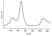
도 7은 GaN을 기재로 한 연속층을 가진, 청색광을 방출하는 반도체 바디의 방출 스펙트럼을 개략적으로 도시한 개략도이고,7 is a schematic diagram schematically showing an emission spectrum of a semiconductor body emitting blue light having a continuous layer based on GaN,
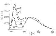
도 8은 백색광을 방출하는, 본 발명에 따른 2개의 반도체 소자의 방출 스펙트럼을 개략적으로 도시한 개략도이며,8 is a schematic diagram schematically showing an emission spectrum of two semiconductor devices according to the present invention, emitting white light,
도 9는 청색광을 방출하는 반도체 바디의 개략적인 단면도이고,9 is a schematic cross-sectional view of a semiconductor body emitting blue light,
도 10은 본 발명에 따른 반도체 소자의 제 7실시예의 개략적인 단면도이며,10 is a schematic cross-sectional view of a seventh embodiment of a semiconductor device according to the present invention;
도 11은 혼색의 적색광을 방출하는 본 발명에 따른 반도체 소자의 방출 스펙트럼을 개략적으로 도시한 개략도이고,11 is a schematic diagram schematically showing an emission spectrum of a semiconductor device according to the present invention for emitting mixed red light;
도 12는 백색광을 방출하는 본 발명에 따른 추가 반도체 소자의 방출 스펙트 럼을 개략적으로 도시한 개략도이며,12 is a schematic diagram schematically showing an emission spectrum of an additional semiconductor device according to the present invention for emitting white light,
도 13은 본 발명에 따른 반도체 소자의 제 8실시예의 개략적인 단면도이고,13 is a schematic cross-sectional view of an eighth embodiment of a semiconductor device according to the present invention;
도 14는 본 발명에 따른 반도체 소자의 제 9실시예의 개략적인 단면도이다.14 is a schematic cross-sectional view of a ninth embodiment of a semiconductor device according to the present invention.
본 발명은 청구범위 청구항 1의 전제부에 따른 발광 반도체 소자에 관한 것이다.The present invention relates to a light emitting semiconductor device according to the preamble of
상기 방식의 반도체 소자는 예컨대 독일 특허 공개 제 38 04 293호에 공지되어 있다. 여기에는 전자 발광 다이오드 또는 레이저 다이오드를 가진 장치가 개시된다. 상기 장치에서는 다이오드로부터 방출되는 모든 방출 스펙트럼이 형광, 광변환 유기 색소와 혼합된 플라스틱 소자에 의해 보다 큰 파장으로 이동된다. 이로 인해, 장치로부터 방출되는 광은 발광 다이오드로부터 방출된 광과는 다른 색을 갖는다. 플라스틱에 첨가되는 색소의 종류에 따라 상이한 색을 발광하는 동일한 발광 다이오드 타입의 발광 다이오드 장치가 제조될 수 있다.Semiconductor devices of this type are known, for example, from German Patent Publication No. 38 04 293. Disclosed is a device having an electron light emitting diode or a laser diode. In the device all emission spectra emitted from the diode are shifted to a larger wavelength by the plastic element mixed with the fluorescence, photoconversion organic dye. As a result, the light emitted from the device has a different color from the light emitted from the light emitting diode. A light emitting diode device of the same light emitting diode type that emits different colors depending on the kind of dye added to the plastic can be manufactured.
독일 특허 공개 제 2 347 289호에는 방출되는 적외선을 가시 광선으로 변환시키는 발광 물질-재료가 적외선 다이오드의 에지에 부착된, 적외선(IR)-고체 램프가 공지되어 있다. 이러한 조치의 목적은, 제어를 위해 방출되는 적외선의 세기를 가급적 적게 감소시키는 동시에, 다이오드로부터 방출되는 적외선의 가급적 적은 부분을 가시 광선으로 변환시키기 위한 것이다.German Patent Publication No. 2 347 289 discloses infrared (IR) -solid lamps in which a luminescent material-material which converts the emitted infrared light into visible light is attached to the edge of the infrared diode. The purpose of this measure is to convert as little of the infrared light emitted from the diode to visible light as possible while reducing the intensity of the infrared light emitted for control as little as possible.
또한, 유럽 특허 제 486 052호에는 기판과 액티브 전자 발광층 사이에 적어도 하나의 반도체 포토 발광 층이 배치된 발광 다이오드가 공지되어 있다. 상기 반도체 포토 발광 층은 액티브 층으로부터 기판의 방향으로 방출되는 제 1 파장 영역의 광을 제 2 파장 영역의 광으로 변환시킴으로써, 발광 다이오드가 전체적으로 상이한 파장 영역의 광을 방출하게 된다.European Patent No. 486 052 also discloses a light emitting diode in which at least one semiconductor photoluminescent layer is arranged between the substrate and the active electroluminescent layer. The semiconductor photo-emitting layer converts light in the first wavelength region emitted from the active layer in the direction of the substrate into light in the second wavelength region, so that the light emitting diode emits light in a whole different wavelength region.
발광 다이오드에 대한 많은 잠재적인 응용 분야에서, 예컨대 자동차 계기판내의 디스플레이 소자, 비행기 및 자동차내의 조명 장치, 그리고 컬러 LED-디스플레이에서, 혼색광, 특히 백색광을 발생시킬 수 있는 발광 다이오드 장치에 대한 요구가 커지고 있다.In many potential applications for light emitting diodes, such as display elements in automotive dashboards, lighting devices in airplanes and automobiles, and color LED-displays, there is a growing need for light emitting diode devices that can generate mixed light, in particular white light. have.
일본 특허 공개 제 07 176 794호에는 백색광을 방출하는 플레이너 광원이 공지되어 있다. 상기 광원에서 투과성 플레이트의 앞면에는 2개의 청색광을 방출하는 다이오드가 배치되고, 상기 다이오드는 광을 투과성 플레이트내로 방출시킨다. 투과성 플레이트의 서로 마주 놓인 2개의 주표면 중 하나는 형광 물질로 코팅되며, 상기 형광 물질은 그것이 다이오드의 청색광에 의해 여기될 때 광을 방출한다. 형광 물질로부터 방출된 광은 다이오드로부터 방출된 청색광과는 다른 파장을 갖는다. 공지된 상기 소자에서는 광원이 균일한 백색광을 방출하도록 형광 물질을 제공하는 것이 매우 어렵다. 또한, 대규모 생산시의 재현가능성에서도 많은 문제점이 있는데, 그 이유는 예컨대, 투과성 플레이트의 표면이 평탄하지 않음으로 인해 형광층의 적은 층두께 변동조차 방출되는 광의 백색 토운(tone)을 변동시키기 때문이다.In Japanese Patent Laid-Open No. 07 176 794, a planar light source that emits white light is known. In the light source two diodes emitting blue light are arranged in front of the transmissive plate, which diode emits light into the transmissive plate. One of the two opposing major surfaces of the transmissive plate is coated with a fluorescent material, which emits light when it is excited by the blue light of the diode. Light emitted from the fluorescent material has a different wavelength from blue light emitted from the diode. In such known devices it is very difficult to provide a fluorescent material so that the light source emits uniform white light. In addition, there are many problems in reproducibility in large-scale production, for example, because the surface of the transmissive plate is uneven, which causes the white tone of light to be emitted even a small variation in the thickness of the fluorescent layer. .
본 발명의 목적은 균일한 혼색광을 방출하고 가급적 재현가능한 소자 특성을 가짐으로써 기술적으로 간단한 대량 생산을 가능하게 하는 반도체 소자를 제공하는 것이다.It is an object of the present invention to provide a semiconductor device which allows for technically simple mass production by emitting uniform mixed light and having reproducible device properties wherever possible.
상기 목적은 청구의범위 청구항 1에 따른 반도체 소자에 의해 달성된다. 본 발명의 바람직한 실시예는 종속청구범위에 제시된다.This object is achieved by a semiconductor device according to
본 발명에 따라 발광 반도체 바디는 연속층, 특히 GaxIn1-xN 또는 GaxAl1-xN로 이루어진 액티브 반도체층을 가진 연속층을 포함하며, 상기 연속층은 반도체 소자의 동작 동안 자외선, 청색 및/또는 녹색 스펙트럼 영역으로부터 제 1 파장 영역의 전자기 광선을 방출한다. 발광 변환 소자는 제 1 파장 영역의 광선의 일부를 제 2 파장 영역의 광선으로 변환시킴으로써, 반도체 소자가 혼색광, 특히 제 1 파장 영역의 광선과 제 2 파장 영역의 광선으로 이루어진 혼색광을 방출한다. 즉, 예컨대 발광 변환 소자가 반도체 바디로부터 방출된 광선의 일부분을 바람직하게는 제 1 파장 영역의 스펙트럼 부분 영역에 걸쳐서만 스펙트럼 선택적으로 흡수하여 긴 파장 영역(제 2 파장 영역)에서 방출한다. 바람직하게 반도체 바디로부터 방출된 광선은 파장 λ ≤ 520㎚에서 상대적인 최대 세기를 가지며, 발광 변환 소자에 의해 스펙트럼 선택적으로 흡수된 파장 영역이 상기 최대 세기 밖에 놓인다.According to the invention the light emitting semiconductor body comprises a continuous layer, in particular a continuous layer having an active semiconductor layer consisting of Gax In1-x N or Gax Al1-x N, said continuous layer being ultraviolet light during operation of the semiconductor device. And emit electromagnetic radiation of the first wavelength region from the blue and / or green spectral region. The light emitting conversion element converts a part of light rays of the first wavelength region into light rays of the second wavelength region so that the semiconductor device emits mixed light, particularly mixed light consisting of light of the first wavelength region and light of the second wavelength region. . That is, for example, the light emitting conversion element absorbs a portion of the light rays emitted from the semiconductor body, preferably only spectral selectively over the spectral partial region of the first wavelength region and emits it in the long wavelength region (second wavelength region). Preferably, the light rays emitted from the semiconductor body have a relative maximum intensity at wavelength λ ≤ 520 nm, and the wavelength region that is spectrally selectively absorbed by the light emitting conversion element lies outside the maximum intensity.
마찬가지로, 바람직하게는 본 발명에 의해 제 1 파장 영역으로부터 유래하는 소수의(하나 또는 다수의) 제 1 스펙트럼 부분 영역이 다수의 제 2 파장 영역으로 변환될 수 있다. 이로 인해, 바람직하게는 여러 가지의 색 혼합 및 색 온도를 발생시키는 것이 가능하다.Likewise, few (one or more) first spectral subregions, preferably from the first wavelength region, can be converted into multiple second wavelength regions by the present invention. For this reason, it is possible to generate various color mixing and color temperature preferably.
본 발명에 따른 반도체 소자는 특히, 발광 변환을 통해 발생된 파장 스펙트럼 및 그에 따라 방출되는 광의 색이 반도체 바디를 통해 흐르는 동작 전류의 세기에 의존하지 않는다는 장점을 갖는다. 이것은 특히 반도체 소자의 주변 온도 및 동작 전류 세기가 크게 변동되는 경우에 큰 의미를 갖는다. 특히, GaN을 기재로 하는 반도체 바디를 가진 발광 다이오드가 이것에 대해 매우 민감하다.The semiconductor device according to the invention has the advantage, in particular, that the wavelength spectrum generated through the luminous conversion and the color of the light emitted accordingly do not depend on the intensity of the operating current flowing through the semiconductor body. This is particularly significant when the ambient temperature and the operating current intensity of the semiconductor element are greatly varied. In particular, light emitting diodes with a semiconductor body based on GaN are very sensitive to this.
또한, 본 발명에 따른 반도체 소자가 단 하나의 트리거 전압 및 그에 따라 단 하나의 트리거 회로 장치만을 필요로 함으로써, 반도체 소자의 트리거 회로에 대한 부품 비용이 매우 적게 유지될 수 있다.In addition, since the semiconductor device according to the present invention requires only one trigger voltage and thus only one trigger circuit device, the component cost for the trigger circuit of the semiconductor device can be kept very low.
본 발명의 특히 바람직한 실시예에서, 반도체 바디 위의 또는 반도체 바디 상의 발광 변환 소자로서는 광선을 방출하는 반도체 바디로부터 방출된 광선에 대해 부분적으로 투과적인 발광 변환층이 제공된다. 방출된 광의 단일 색을 보장하기 위해, 바람직하게는 발광 변환층이 일정한 두께를 갖도록 형성된다. 이것은 발광 변환층을 통해 반도체 바디로부터 방출되는 광의 경로 길이가 모든 방출 방향으로 거의 일정하다는 장점을 갖는다. 이로 인해, 반도체 소자가 모든 방향으로 동일한 색의 광을 방출할 수 있다. 상기 개선예에 따른 본 발명의 반도체 소자의 또다른 장점은 간단한 방식으로 높은 재현가능성이 얻어질 수 있다는 것이다. 이것은 효과적인 대량 생산을 위해 중요하다. 발광 변환층으로서는 예컨대 발광 물질 과 혼합된 래커층 또는 수지층이 제공될 수 있다.In a particularly preferred embodiment of the invention, the light emitting conversion element on or on the semiconductor body is provided with a light emitting conversion layer partially transmissive to the light emitted from the semiconductor body emitting the light. In order to ensure a single color of emitted light, the light emitting conversion layer is preferably formed to have a constant thickness. This has the advantage that the path length of the light emitted from the semiconductor body through the light emitting conversion layer is almost constant in all emission directions. As a result, the semiconductor element can emit light of the same color in all directions. Another advantage of the semiconductor device of the present invention according to the above improvement is that high reproducibility can be obtained in a simple manner. This is important for effective mass production. As the light emitting conversion layer, for example, a lacquer layer or a resin layer mixed with the light emitting material may be provided.
본 발명에 따른 반도체 소자의 다른 바람직한 실시예는 발광 변환 소자로서 반투과성 발광 변환 커버링을 포함한다. 상기 발광 변환 커버링은 반도체 바디의 적어도 일부(및 경우에 따라 전기 접속부의 부분 영역)를 둘러싸는 동시에 부품 커버링(하우징)으로서 사용될 수 있다. 이 실시예에 따른 반도체 소자의 장점은, 종래의 발광 다이오드(예컨대, 레이디얼 발광 다이오드)를 제조하기 위해 사용되는 종래의 제조 라인이 상기 반도체 소자의 제조를 위해서도 사용될 수 있다는 것이다. 부품의 커버링을 위해, 종래의 발광 다이오드에서 사용된 투과성 플라스틱 대신, 발광 변환 커버링의 재료가 사용된다.Another preferred embodiment of the semiconductor device according to the invention comprises a translucent light emitting conversion covering as a light emitting conversion element. The light emission conversion covering can be used as a part covering (housing) at the same time surrounding at least a portion of the semiconductor body (and optionally a partial region of the electrical connection). An advantage of the semiconductor device according to this embodiment is that a conventional manufacturing line used for manufacturing a conventional light emitting diode (eg, a radial light emitting diode) can also be used for manufacturing the semiconductor device. For the covering of the part, instead of the transmissive plastic used in conventional light emitting diodes, the material of the light emission conversion covering is used.
본 발명에 따른 반도체 소자의 다른 바람직한 실시예 및 2개의 상기 실시예에서, 발광 변환층 또는 발광 변환 커버링은 적어도 하나의 발광 물질을 포함하는(바람직한 플라스틱 및 발광 물질의 예는 하기에 제시된다) 투과성 재료, 예컨대 플라스틱, 바람직하게는 에폭시수지로 이루어진다. 따라서, 발광 변환 소자가 특히 저렴하게 제조될 수 있다. 제조를 위해 필요한 단계들이 큰 비용 없이 발광 다이오드를 위한 종래의 생산 라인에 통합될 수 있다.In another preferred embodiment of the semiconductor device according to the invention and in the two above embodiments, the light emitting conversion layer or the light emitting conversion covering comprises at least one light emitting material (an example of a preferred plastic and a light emitting material is given below). Material, such as plastic, preferably epoxy resin. Therefore, the light emitting conversion element can be manufactured particularly inexpensively. The steps necessary for manufacturing can be integrated into a conventional production line for light emitting diodes without significant cost.
본 발명의 특히 바람직한 실시예 또는 전술한 실시예에서, 제 2 파장 영역은 제 1 파장 영역보다 훨씬 더 큰 파장을 갖는다.In a particularly preferred embodiment of the invention or in the foregoing embodiments, the second wavelength region has a much larger wavelength than the first wavelength region.
특히, 제 1 파장 영역의 제 2 스펙트럼 서브 영역 및 제 2 파장 영역은 서로 상보적이다. 이렇게 함으로써, 청색광을 방출하는 단 하나의 반도체 바디를 가진 단색 광원, 특히 발광 다이오드로부터 혼색, 특히 백색광이 발생될 수 있다. 청색 광을 방출하는 반도체 바디로 백색광을 발생시키기 위해, 반도체 바디로부터 방출되는 광선의 일부분이 청색 스펙트럼 영역으로부터 청색에 대한 보색인 황색 스펙트럼 영역으로 변환된다. 백색광의 색 온도 또는 색 로커스는 발광 변환 소자의 선택에 의해서, 특히 발광 물질, 그것의 입자 크기 및 그것의 농도의 적합한 선택에 의해 변동될 수 있다. 또한, 상기 배열 상태는 바람직하게는 발광 물질 혼합물을 사용할 수 있는 가능성을 제공하므로, 바람직하게는 원하는 컬러 토운이 매우 정확히 세팅될 수 있다. 마찬가지로, 발광 변환 소자는 예컨대 불균일한 발광 물질 분포에 의해 불균일하게 형성될 수 있다. 이로 인해, 발광 변환 소자에 의한 광의 상이한 경로 길이가 바람직하게 보상될 수 있다.In particular, the second spectral subregion and the second wavelength region of the first wavelength region are complementary to each other. By doing so, mixed color, in particular white light, can be generated from a monochromatic light source, in particular a light emitting diode, having only one semiconductor body emitting blue light. To generate white light with a semiconductor body that emits blue light, a portion of the light rays emitted from the semiconductor body are converted from a blue spectral region to a yellow spectral region that is complementary to blue. The color temperature or color locus of the white light can be varied by the choice of the luminous conversion element, in particular by the appropriate choice of the luminescent material, its particle size and its concentration. In addition, the arrangement state preferably offers the possibility of using a mixture of luminescent materials, so that the desired color tone can be set very precisely. Likewise, the light emitting conversion element can be formed nonuniformly, for example, by nonuniform light emitting material distribution. Due to this, different path lengths of light by the light emitting conversion element can be preferably compensated for.
본 발명에 따른 반도체 소자의 다른 바람직한 실시예에서, 발광 변환 소자 또는 부품 커버링의 다른 구성 부분은 색의 매칭을 위해 하나 또는 다수의 색소를 포함한다. 상기 색소는 파장 변환에 영향을 미치지 않는다. 이를 위해서, 종래의 발광 다이오드를 제조하기 위해 사용된 색소, 예컨대 아조-, 안트라퀴논- 또는 페리논-색소가 사용될 수 있다.In another preferred embodiment of the semiconductor device according to the invention, the other constituent parts of the luminous conversion element or part covering comprise one or several pigments for color matching. The pigment does not affect wavelength conversion. For this purpose, the pigments used for producing conventional light emitting diodes such as azo-, anthraquinone- or perinone-pigments can be used.
지나치게 높은 광선 부하로부터 발광 변환 소자를 보호하기 위해, 바람직한 실시예에서 또는 본 발명에 따른 반도체 소자의 전술한 바람직한 실시예에서 반도체 바디의 표면의 적어도 일부분이 예컨대 플라스틱으로 이루어진 제 1투과성 커버에 의해 둘러싸인다. 상기 투과성 커버상에 발광 변환층이 제공된다. 이로 인해, 발광 변환 소자내에서의 광선 밀도 및 상기 소자의 광선 부하가 감소되며, 이것은 사용되는 재료에 따라 발광 변환 소자의 수명에 긍정적으로 작용한다.In order to protect the light emitting conversion element from an excessively high light load, in a preferred embodiment or in the above-described preferred embodiment of the semiconductor device according to the invention at least a part of the surface of the semiconductor body is surrounded by a first transparent cover, for example made of plastic. All. A light emitting conversion layer is provided on the transparent cover. This reduces the light density in the light emitting conversion element and the light load of the device, which positively affects the life of the light emitting conversion element depending on the material used.
본 발명의 특히 바람직한 실시예 및 전술한 실시예에서, 방출된 광선 스펙트럼이 420nm 내지 460nm, 특히 430nm(예컨대, GaxAl1-xN을 기재로 하는 반도체 바디) 또는 450nm(예컨대, GaxIn1-xN을 기재로 하는 반도체 바디)의 파장에서 최대 세기를 갖는 발광 반도체 바디가 사용된다. 이러한 본 발명에 따른 반도체 소자에 의해, 바람직하게는 거의 모든 색 및 C.I.E.-색 챠트의 혼색이 발생될 수 있다. 여기서, 발광 반도체 바디는 전술한 바와 같이 전자 발광 반도체 재료 및 다른 전자 발광 재료, 예컨대 중합체 재료로 이루어진다.In a particularly preferred embodiment of the invention and in the embodiments described above, the emitted light spectrum is between 420 nm and 460 nm, in particular 430 nm (eg semiconductor body based on Gax Al1-x N) or 450 nm (eg Gax In A light emitting semiconductor body having a maximum intensity at the wavelength of the semiconductor body based on1-x N is used. By means of this semiconductor device according to the invention, preferably mixing of almost all colors and CIE-color charts can occur. Here, the light emitting semiconductor body is made of an electroluminescent semiconductor material and another electroluminescent material such as a polymer material as described above.
본 발명의 다른 특히 바람직한 실시예에서 발광 변환 커버링 또는 발광 변환층은 래커 또는 플라스틱 예컨대, 광전 소자의 커버링에 사용되는 실리콘(silicone) 재료, 열가소성 재료 또는 열경화성 플라스틱 재료(에폭시수지 및 아크릴레이트수지)로 제조된다. 예컨대, 열가소성 재료로 제조된 커버링이 발광 변환 커버링으로 사용될 수 있다. 전술한 모든 재료는 간단한 방식으로 하나 또는 다수의 발광 물질과 혼합될 수 있다.In another particularly preferred embodiment of the invention the luminous conversion covering or luminous conversion layer is made of a lacquer or plastic such as silicone material, thermoplastic material or thermosetting plastic material (epoxy resin and acrylate resin) used for covering photovoltaic devices. Are manufactured. For example, a covering made of thermoplastic material can be used as the light emission conversion covering. All of the materials described above can be mixed with one or more luminescent materials in a simple manner.
반도체 바디가 경우에 따라 미리 제조된 하우징의 리세스내에 배치되고, 발광 변환층을 포함하는 커버링이 상기 리세스에 제공되면, 본 발명에 따른 반도체 소자가 매우 간단히 구현될 수 있다. 이러한 반도체 소자는 종래의 생산 라인에서 대량으로 제조될 수 있다. 또한, 커버링의 하우징내에 반도체 바디를 조립한 후에만 예컨대 하나의 래커층 또는 주조 수지층 또는 열가소성 재료로 미리 제조된 커버링 플레이트가 하우징상에 제공되어야 한다. 옵션으로서, 하우징의 리세스가 투과성 재료, 예컨대 투과성 플라스틱으로 채워질 수 있다. 상기 투과성 재료는 특 히 반도체 바디로부터 방출되는 광의 파장을 변동시키지 않거나 또는 필요한 경우에는 발광를 변환시키도록 형성될 수 있다.If the semiconductor body is optionally disposed in a recess of a prefabricated housing and a covering comprising a light emitting conversion layer is provided in the recess, the semiconductor device according to the invention can be implemented very simply. Such semiconductor devices can be manufactured in large quantities in conventional production lines. In addition, only after assembling the semiconductor body in the housing of the covering, a covering plate prepared in advance of, for example, one lacquer layer or cast resin layer or thermoplastic material should be provided on the housing. As an option, the recess of the housing can be filled with a permeable material, such as a permeable plastic. The transmissive material may in particular be formed so as not to vary the wavelength of light emitted from the semiconductor body or to convert luminescence if necessary.
매우 간단한 구현 가능성으로 인해, 본 발명에 따른 바람직한 반도체 소자의 실시예에서 반도체 바디는 경우에 따라 미리 제조된, 실제로 이미 리드 프레임을 가진 하우징의 리세스내에 배치되며, 리세스는 적어도 반투명의 주조 수지로 채워진다. 상기 주조 수지에는 리세스의 주조 전에 이미 발광 물질이 첨가된다. 따라서, 발광 변환 소자는 반도체 바디를 발광 물질과 함께 주조함으로써 제조된다.Due to the very simple feasibility, in an embodiment of the preferred semiconductor device according to the invention the semiconductor body is in some cases pre-fabricated, in fact arranged in a recess of a housing already having a lead frame, the recess being at least translucent cast resin. Filled with. The cast resin is already added with a luminescent material before the casting of the recess. Therefore, the light emitting conversion element is manufactured by casting the semiconductor body together with the light emitting material.
발광 변환 소자를 제조하기 위한 특히 바람직한 재료는 하나 또는 다수의 발광 물질이 첨가된 에폭시수지이다. 그러나, 에폭시수지 대신에 폴리메틸메타크릴레이트(PMMA)가 사용될 수도 있다.Particularly preferred materials for producing light emitting conversion elements are epoxy resins to which one or more light emitting materials are added. However, polymethyl methacrylate (PMMA) may be used instead of the epoxy resin.
PMMA는 간단한 방식으로 유기 색소 분자와 혼합될 수 있다. 본 발명에 따른 녹색, 황색 및 적색 발광 반도체 소자의 제조를 위해, 예컨대 페릴렌을 기재로 하는 색소 분자가 사용될 수 있다. 자외선, 가시 광선 또는 적외선에서 발광하는 반도체 소자는 4f-유기 금속 화합물의 혼합에 의해서도 제조될 수 있다. 특히, 본 발명에 따른 적색 발광 반도체 소자는 예컨대 Eu3+를 기재로 하는 유기 금속 킬레이트(λ ≒ 620nm)의 혼합에 의해 구현될 수 있다. 특히 청색광을 방출하는 반도체 바디를 가진 본 발명에 따른 적외선 발광 반도체 소자는 4f-킬레이트 또는 Ti3+-도핑된 사파이어의 혼합에 의해 제조될 수 있다.PMMA can be mixed with organic pigment molecules in a simple manner. For the production of green, yellow and red light emitting semiconductor devices according to the invention, for example, pigment molecules based on perylene can be used. Semiconductor devices emitting light in ultraviolet light, visible light or infrared light can also be produced by mixing 4f-organic metal compounds. In particular, the red light emitting semiconductor device according to the present invention can be implemented by mixing an organometallic chelate (λ ≒ 620 nm) based on, for example, Eu3+ . In particular, an infrared light emitting semiconductor device according to the invention with a semiconductor body emitting blue light can be produced by mixing 4f-chelate or Ti3+ -doped sapphire.
백색광을 방출하는 본 발명에 따른 반도체 소자는 바람직하게는, 반도체 바디로부터 방출된 청색광선이 상보의 파장 영역으로, 특히 청색과 황색으로 또는 부가의 삼원색(triad), 예컨대 청색, 녹색 및 적색으로 변환되도록 발광 물질이 선택됨으로써 제조될 수 있다. 여기서, 황색 또는 녹색 및 적색광은 발광 물질에 의해 발생될 수 있다. 이로 인해 발생되는 백색광의 컬러 토운(CIE-색 챠트내의 색 로커스)은 혼합 및 농도와 관련하여 색소(들)을 적합하게 선택함으로써 변동될 수 있다.The semiconductor device according to the invention which emits white light preferably preferably converts the blue light emitted from the semiconductor body into the complementary wavelength region, in particular blue and yellow or additional triads such as blue, green and red The luminescent material may be prepared by selecting one. Here, yellow or green and red light may be generated by the light emitting material. The resulting color tones of the white light (color locus in the CIE-color chart) can be varied by suitably selecting the dye (s) with respect to mixing and concentration.
백색광을 방출하는 본 발명에 따른 반도체 소자용으로 적합한 유기 발광 물질은 페릴렌 발광 물질이다. 예컨대 녹색 발광용으로 BASF Lumogen F 083, 황색 발광용으로는 BASF Lumogen F 240 및 적색 발광용으로는 BASF Lumogen F 300이 있다. 이러한 색소는 간단한 방식으로 예컨대 투과성 에폭시수지에 첨가될 수 있다.Suitable organic light emitting materials for semiconductor devices according to the invention which emit white light are perylene light emitting materials. For example, BASF Lumogen F 083 for green light emission, BASF Lumogen F 240 for yellow light emission, and BASF Lumogen F 300 for red light emission. Such pigments may be added to the permeable epoxy resin in a simple manner, for example.
청색광을 방출하는 반도체 바디로 녹색광을 방출하는 반도체 소자를 제조하기 위한 바람직한 방법은 발광 변환 소자에 UO2++-치환된 붕소 실리케이트 유리를 사용하는 것이다.A preferred method for manufacturing a semiconductor device emitting green light with a semiconductor body emitting blue light is to use UO2 ++ -substituted boron silicate glass in the light emitting conversion device.
본 발명에 따른 반도체 소자의 다른 바람직한 실시예 또는 전술한 바람직한 실시예에서는, 발광 변환 소자 또는 다른 부품 커버링의 광투과성 부품에 부가로 광산란 입자, 소위 확산체가 첨가된다. 이로 인해, 바람직하게는 반도체 소자의 색 효과 및 방출 특성이 최적화될 수 있다.In another preferred embodiment of the semiconductor device according to the invention or in the above-described preferred embodiment, light scattering particles, so-called diffusers, are added to the light transmissive component of the light emitting conversion element or other component covering. For this reason, the color effect and emission characteristic of the semiconductor device can be optimized optimally.
본 발명에 따른 반도체 소자의 특히 바람직한 실시예에서, 발광 변환 소자는 적어도 부분적으로 무기 발광 물질을 포함하는 투과성 에폭시수지로 이루어진다. 바람직하게는 무기 발광 물질이 간단한 방식으로 에폭시수지 내에 결합될 수 있다. 본 발명에 따른 백색 발광 반도체 소자를 제조하기 위한 특히 바람직한 무기 발광 물질은 형광체 YAG:Ce(Y3Al5O12:Ce3+) 이다. 이것은 매우 간단한 방식으로 LED-기술에 사용되는 종래의 투과성 에폭시수지에 혼합될 수 있다. 또한, 희토류로 도핑된 다른 그라네이트, 예컨대 Y3Ga5O12:Ce3+, Y(Al,Ga)5O12:Ce3+ 및 Y(Al,Ga)5O12:Tb3+ 및 희토류로 도핑된 알칼리토금속황화물, 예컨대 SrS:Ce3+, Na, SrS:Ce3+, Cl, SrS:CeCl3, CaS:Ce3+ 및 SrSe:Ce3+가 발광 물질로 사용될 수 있다.In a particularly preferred embodiment of the semiconductor device according to the invention, the luminous conversion element consists of a transmissive epoxy resin comprising at least partly an inorganic light emitting material. Preferably, the inorganic light emitting material may be bonded in the epoxy resin in a simple manner. Particularly preferred inorganic light emitting material for producing a white light emitting semiconductor device according to the present invention is phosphor YAG: Ce (Y3 Al5 O12 : Ce3+ ). It can be mixed in conventional transmissive epoxy resins used in LED technology in a very simple manner. In addition, other granates doped with rare earths such as Y3 Ga5 O12 : Ce3+ , Y (Al, Ga)5 O12 : Ce3+ and Y (Al, Ga)5 O12 : Tb3+ and Alkaline earth metal sulfides doped with rare earths such as SrS: Ce3+ , Na, SrS: Ce3+ , Cl, SrS: CeCl3 , CaS: Ce3+ and SrSe: Ce3+ can be used as luminescent materials.
상이한 혼색광을 발생시키기 위해서는, 희토류로 도핑된 티오갈레이트, 예컨대 CaGa2S4:Ce3+ 및 SrGa2S4:Ce3+가 특히 적합하다. 마찬가지로, 희토류로 도핑된 알루미네이트, 예컨대 YAlO3:Ce3+, YGaO3:Ce3+, Y(Al,Ga)O3:Ce3+ 및 희토류로 도핑된 오르토실리케이트 M2SiO5:Ce3+(M:Sc, Y, Sc), 예컨대 Y2SiO5:Ce3+도 사용될 수 있다. 모든 이트륨 화합물에서 이트륨은 스칸듐 또는 란탄으로 치환될 수 있다.In order to generate different mixed light, thiogallate doped with rare earths such as CaGa2 S4 : Ce3+ and SrGa2 S4 : Ce3+ are particularly suitable. Likewise, rare earth doped aluminates such as YAlO3 : Ce3+ , YGaO3 : Ce3+ , Y (Al, Ga) O3 : Ce3+ and orthosilicate M2 SiO5 : Ce3 doped with rare earths+ (M: Sc, Y, Sc), such as Y2 SiO5 : Ce3+ , may also be used. In all yttrium compounds yttrium may be substituted with scandium or lanthanum.
본 발명에 따른 반도체 소자의 다른 실시예에서, 적어도 모든 커버링의 발광 부품, 즉 발광 변환 커버링 또는 층은 순수한 무기 재료로 이루어진다. 따라서, 발광 변환 소자는 온도에 안정적인, 투과성 또는 반투과성 무기 재료내에 매립된 무기 발광 물질로 이루어진다. 특히, 발광 변환 소자는 바람직하게는 저융점 무기 유리(예컨대, 실리케이트 유리)내에 매립된 무기 형광체로 이루어진다. 이러한 발광 변환층에 대한 바람직한 제조 방법은 전체 발광 변환층, 즉 무기 발광 물질 및 매립 재료를 하나의 공정으로 제조할 수 있는 졸-겔 기술이다.In another embodiment of the semiconductor device according to the invention, at least all the light emitting components of the covering, ie the light emitting conversion covering or layer, are made of a pure inorganic material. Accordingly, the light emitting conversion element is made of an inorganic light emitting material embedded in a transparent or semipermeable inorganic material that is temperature stable. In particular, the light emitting conversion element preferably consists of an inorganic phosphor embedded in a low melting inorganic glass (eg, silicate glass). A preferred manufacturing method for such a light emitting conversion layer is a sol-gel technique capable of manufacturing the entire light emitting conversion layer, that is, an inorganic light emitting material and a buried material in one process.
반도체 바디로부터 방출되는 제 1 파장 영역의 광선과 발광 변환된 제 2 파장 영역 광선의 혼합 및 그에 따라 방출되는 광의 색 균일성을 개선시키기 위해, 본 발명에 따른 반도체 소자의 바람직한 실시예에서 부가로 반도체 바디로부터 방 출되는 광선의 소위 방향 특성을 약화시키는 청색 발광 색소가 발광 커버링 또는 발광 변환층 및/또는 부품 커버링의 다른 구성 부분에 첨가된다. 상기 방향 특성은 반도체 바디로부터 방출되는 광선이 바람직한 방출 방향을 갖는다는 것을 의미한다.In addition, in a preferred embodiment of the semiconductor device according to the present invention, in order to improve the mixing of the light of the first wavelength region emitted from the semiconductor body with the light-converted second wavelength region radiation and thus the color uniformity of the light emitted, Blue luminescent pigments are added to the luminescent covering or luminescent conversion layer and / or other constituent parts of the component covering which weaken the so-called directional properties of the light emitted from the body. The directional characteristic means that the light rays emitted from the semiconductor body have a preferred emission direction.
본 발명에 따른 반도체 소자의 바람직한 실시예에서, 전술한 바와 같이 방출되는 광선을 혼합하기 위해 분말형 무기 발광 물질이 사용된다. 이 경우, 발광 물질 입자는 그것을 둘러싸는 물질(매트릭스)내에서 용해되지 않는다. 또한, 무기 발광 물질 및 그것을 둘러싸는 물질은 서로 상이한 굴절률을 갖는다. 이것은 바람직하게는 발광 물질의 입자 크기에 따라 발광 물질에 의해 흡수되지 않은 광의 성분이 산란되게끔 한다. 이로 인해, 반도체 바디로부터 방출되는 광선의 방향 특성이 효율적으로 약화됨으로써, 흡수되지 않은 광선 및 발광 변환된 광선이 균일하게 혼합되며, 이것은 공간적으로 균일한 색 효과를 야기한다.In a preferred embodiment of the semiconductor device according to the invention, a powdered inorganic light emitting material is used to mix the emitted light rays as described above. In this case, the luminescent material particles do not dissolve in the material (matrix) surrounding it. In addition, the inorganic light emitting material and the material surrounding it have different refractive indices. This preferably causes the components of light not absorbed by the luminescent material to be scattered, depending on the particle size of the luminescent material. This effectively weakens the directional characteristics of the light rays emitted from the semiconductor body, whereby unabsorbed light rays and light emission converted light rays are uniformly mixed, which causes a spatially uniform color effect.
백색광을 방출하는 본 발명에 따른 반도체 소자는, 발광 변환 커버링 또는 발광 변환층의 제조에 사용되는 에폭시수지에 무기 발광 물질 YAG:Ce (Y3Al5O12:Ce3+)이 혼합됨으로써 매우 바람직하게 구현될 수 있다. 반도체 바디로부터 방출되는 청색 광선의 일부분이 무기 발광 물질 Y3Al5O12:Ce3+로부터 황색 스펙트럼으로 그리고 그에 따라 청색에 대한 보색인 파장 영역으로 이동된다. 백색광의 컬러 토운(CIE-색 챠트내의 색 로커스)은 색소 혼합 및 색소 농도의 적합한 선택에 의해서 변동될 수 있다.The semiconductor device according to the present invention, which emits white light, is very preferable because the inorganic light emitting material YAG: Ce (Y3 Al5 O12 : Ce3+ ) is mixed with an epoxy resin used for the emission conversion covering or the manufacture of the emission conversion layer. Can be implemented. A portion of the blue light emitted from the semiconductor body is shifted from the inorganic light emitting material Y3 Al5 O12 : Ce3+ in the yellow spectrum and thus in the wavelength region which is complementary to blue. The color tones of the white light (color locus in the CIE-color chart) can be varied by suitable choice of pigment mixing and pigment concentration.
무기 발광 물질 YAG:Ce는 특히 약 1.84의 굴절률을 가진 불용성 안료(10μm 범위의 입자 크기)가 사용된다는 장점을 갖는다. 이로 인해, 파장 변환과 더불어 청색 다이오드 광선 및 황색 컨버터 광선을 제대로 혼합시키는 산란 효과가 나타난다.The inorganic luminescent material YAG: Ce has the advantage in particular that an insoluble pigment (particle size in the range of 10 μm) with a refractive index of about 1.84 is used. This results in a wavelength conversion and a scattering effect of properly mixing the blue diode light and the yellow converter light.
본 발명에 따른 다른 바람직한 실시예 또는 전술한 바람직한 실시예에서, 발광 변환 소자 또는 부품 커버링의 다른 광투과성 부품에는 부가로 광산란 입자, 소위 확산체가 첨가된다. 이로 인해, 바람직하게는 반도체 소자의 색 효과 및 방출 특성이 더욱 최적화된다.In another preferred embodiment according to the invention or in the preferred embodiment described above, light-scattering particles, so-called diffusers, are additionally added to the light emitting conversion element or other light transmissive component of the component covering. For this reason, the color effect and emission characteristic of the semiconductor element are preferably further optimized.
백색광을 방출하는 본 발명에 따른 반도체 소자의 발광 효과 또는 GaN을 기재로 하여 제조된 청색 발광 반도체 바디를 가진 상기 실시예의 발광 효과는 전구의 발광 효과와 필적할 만하다는 것이 특히 바람직하다. 그 이유는, 한편으로는 이러한 반도체 바디의 외부 양자 수율의 퍼센트가 낮고, 다른 한편으로는 유기 색소 분자의 발광 수율의 퍼센트가 90% 이상이 되기 때문이다. 또한, 본 발명에 따른 반도체 소자는 전구에 비해 극도로 긴 수명, 큰 강성 및 작은 작동 전압을 특징으로 한다.It is particularly preferred that the luminous effect of the semiconductor device according to the invention emitting white light or the luminous effect of this embodiment with a blue luminous semiconductor body made on the basis of GaN is comparable to the luminous effect of the bulb. This is because, on the one hand, the percentage of external quantum yield of such a semiconductor body is low, and on the other hand, the percentage of luminescence yield of organic dye molecules becomes 90% or more. In addition, the semiconductor device according to the invention is characterized by an extremely long life, a large stiffness and a small operating voltage compared to the bulb.
또한, 사람의 눈으로 감지할 수 있는 본 발명에 따른 반도체 소자의 명도가 발광 변환 소자를 갖지 않은 동일한 반도체 소자에 비해 현저히 증가될 수 있다는 것이 바람직한데, 그 이유는 파장이 클수록 눈의 감도가 커지기 때문이다.In addition, it is preferable that the brightness of the semiconductor device according to the present invention, which can be detected by the human eye, can be significantly increased compared to the same semiconductor device without the light-emitting conversion device, because the larger the wavelength, the greater the sensitivity of the eye. Because.
또한, 본 발명에 따른 원리에 의해 바람직하게는 반도체 바디로부터 가시 광선과 함께 방출되는 자외선이 가시 광선으로 변환될 수 있다. 이로 인해, 반도체 바디로부터 방출되는 광의 명도가 현저히 증가된다.Furthermore, by the principle according to the invention preferably ultraviolet rays emitted with visible light from the semiconductor body can be converted into visible light. This significantly increases the brightness of the light emitted from the semiconductor body.
반도체 소자의 청색광에 의해 이루어지는 발광 변환은 바람직하게는, 자외선 → 청색 → 녹색 → 황색 → 적색의 방식에 따라 다단계 발광 변환 소자들로 확대될 수도 있다. 이 경우 다수의 스펙트럼 선택적 방출 발광 변환 소자가 반도체 바디에 상대적으로 차례로 배치된다.The light emission conversion made by the blue light of the semiconductor element may preferably be extended to the multilevel light emission conversion elements in the manner of ultraviolet light → blue → green → yellow → red. In this case, a plurality of spectral selective emission light emitting conversion elements are arranged in turn relative to the semiconductor body.
마찬가지로, 바람직하게는 다수의 상이한 스펙트럼 선택적 방출 색소 분자가 발광 변환 소자의 하나의 투과성 플라스틱 내에 공통적으로 매립될 수 있다. 그럼으로써, 매우 넓은 컬러 스펙트럼이 형성될 수 있다.Likewise, preferably a number of different spectral selective emission pigment molecules may be commonly embedded in one transmissive plastic of the luminous conversion element. As a result, a very broad color spectrum can be formed.
발광 변환 색소로서 특히 YAG:Ce가 사용되는, 본 발명에 따른 백색광을 방출하는 반도체 소자의 특별한 장점은, 청색광의 여기시 상기 발광 재료가 흡수와 방출 사이에 약 100nm의 스펙트럼 이동을 야기한다는 것이다. 이것은 발광 재료로부터 방출되는 광의 재흡수를 감소시키고 그에 따라 높은 광 수율을 야기한다. 또한, YAG:Ce는 바람직하게는 높은 열적 및 광화학적(예컨대, 자외선) 안정성(유기 발광 재료 보다 현저히 높음)을 가지므로, 외부 용도 및/또는 큰 온도 범위용 백색 발광 다이오드가 제조될 수 있다.A particular advantage of the semiconductor device emitting white light according to the invention, in which YAG: Ce is used in particular as the emission conversion dye, is that, upon excitation of blue light, the light emitting material causes a spectral shift of about 100 nm between absorption and emission. This reduces the reabsorption of light emitted from the luminescent material and thus causes a high light yield. In addition, YAG: Ce preferably has high thermal and photochemical (eg ultraviolet) stability (significantly higher than organic light emitting materials), so that white light emitting diodes for external applications and / or large temperature ranges can be produced.
YAG:Ce는 지금까지 재흡수, 광 수율, 열적 및 광화학적 안정성 및 처리 가능성면에서 최상으로 적합한 발광 물질로 나타났다. 그러나, 다른 Ce 도핑된 형광체, 특히 Ce 도핑된 그라네이트가 사용될 수도 있다.YAG: Ce has been shown to be the most suitable luminescent material so far in terms of resorption, light yield, thermal and photochemical stability and treatability. However, other Ce doped phosphors, in particular Ce doped granates, may also be used.
본 발명에 따른 반도체 소자는 특히 컬러 LED-디스플레이에서 그것의 낮은 전력 소비로 인해 자동차 실내 조명 또는 비행기 객실의 조명 장치에 그리고 자동차 계기판 또는 액정 디스플레이와 같은 디스플레이 장치의 조명 장치에 특히 바람 직하게 사용될 수 있다.The semiconductor device according to the invention can be particularly preferably used in lighting devices in automotive interior lighting or in airplane cabins and in lighting devices of display devices such as automotive instrument clusters or liquid crystal displays due to its low power consumption, especially in color LED displays. have.
본 발명의 추가 특징, 장점 및 바람직한 실시예는 첨부된 도면과 연관된 하기 실시예 설명에 제시된다.Further features, advantages and preferred embodiments of the invention are set forth in the following description of the embodiments in conjunction with the accompanying drawings.
여러 도면에서 동일한 부분 또는 동일하게 작용하는 부분은 언제나 동일한 도면 부호로 표기하였다.In the drawings, the same or identically-functioning parts are always denoted by the same reference numerals.
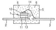
도 1에 도시된 광을 방출하는 반도체 소자에서 반도체 바디(1)는 후면 콘택(11), 전면 콘택(12) 및 소수의 상이한 층으로 이루어진 연속층(7)을 포함하며, 상기 연속층은 반도체 소자의 동작 동안 광선(예를 들어 자외 광선, 청색 광선 또는 녹색 광선)을 방출하는 적어도 하나의 액티브 영역을 포함한다.In the semiconductor device emitting light shown in FIG. 1, the
본 실시예 및 하기에 기술된 모든 실시예에 적합한 연속층(7)에 대한 일 실시예는 도 9에 도시되었다. 상기 실시예에서 예를 들어 SiC로 이루어진 기판(18)상에는 AlN-층 또는 GaN-층(19), n-도전성 GaN-층(20), n-도전성 GaxAl1-XN-층 또는 GaXIn1-XN-층(21), 추가의 n-도전성 GaN-층 또는 GaXIn1-XN-층(22), p-도전성 GaXAl1-XN-층 또는 GaXIn1-XN-층(23) 및 p-도전성 GaN-층(24)으로 이루어진 연속층이 제공된다. p-도전성 GaN-층(24)의 주표면(25) 및 기판(18)의 주표면(26)상에는 각각 하나씩 콘택 금속층(27, 28)이 제공되는데, 이 콘택 금속층은 통상적으로 광반도체 기술에서 전기 콘택용으로 사용되는 재료로 이루어진다.One embodiment of the continuous layer 7 suitable for this embodiment and all the embodiments described below is shown in FIG. In this embodiment an AlN-layer or GaN-
그러나, 당업자에게 있어서 본 발명에 따른 반도체 소자용으로 적합하다고 생각되는 다른 모든 반도체 바디도 또한 사용될 수 있다. 이것은 하기에 기술된 모든 실시예에도 동일하게 적용된다.However, any other semiconductor body deemed suitable for the semiconductor device according to the invention by one skilled in the art can also be used. This applies equally to all the examples described below.
도 1의 실시예에서 반도체 바디(1)는 도전성 결합 수단, 예컨대 금속 땜납 또는 접착제에 의해 상기 바디의 후면 콘택(11)과 함께 제 1 전기 접속부(2)상에 고정된다. 전면 콘택(12)은 본딩 와이어(14)에 의해 제 2 전기 접속부(3)와 결합된다.In the embodiment of FIG. 1, the
반도체 바디(1)의 노출 표면 및 전기 접속부(2 및 3)의 일부 영역은 발광 변환 커버링(5)에 의해서 직접 둘러싸인다. 상기 발광 변환 커버링은 바람직하게 투과성 발광 다이오드 커버링용으로 사용될 수 있는 투과성 플라스틱(바람직하게는 에폭시수지 또는 폴리메틸메타크릴레이트)으로 이루어지며, 그 플라스틱은 발광 물질(6), 바람직하게는 백색을 발하는 소자를 위한 무기 발광 물질, 특히 Y3Al5O12:Ce3+(YAG:Ce)와 혼합된다.The exposed surface of the
도 2에 도시된 본 발명에 따른 반도체 소자의 실시예는, 반도체 바디(1) 및 전기 접속부(2 및 3)의 일부 영역이 발광 변환 커버링 대신 투과성 커버링(15)에 의해 둘러싸인다는 점에서 도 1의 실시예와 상이하다. 상기 투과성 커버링(15)은 반도체 바디(1)로부터 방출된 광선의 파장 변동에 아무런 영향을 미치지 않으며, 예를 들어 발광 다이오드 기술에서 통상적으로 사용되는 에폭시수지, 실리콘수지 또는 아크릴수지, 혹은 예컨대 무기 유리와 같은 다른 적합한 광투과성 재료로 이루어진다.The embodiment of the semiconductor device according to the invention shown in FIG. 2 is characterized in that part of the
상기 광투과성 커버링(15)상에는 도 2에 도시된 바와 같이 커버링(15)의 전체 표면을 덮는 발광 변환층(4)이 제공된다. 이 발광 변환층(4)이 상기 표면의 일부분만을 덮는 경우도 또한 생각할 수 있다. 발광 변환층(4)은 재차 예를 들어 발 광 물질(6)과 혼합되는 투과성 플라스틱(예를 들면 에폭시수지, 래커 코팅 또는 폴리메틸메타크릴레이트)으로 이루어진다. 이 경우에도 백색을 발하는 반도체 소자용 발광 물질로서는 YAG:Ce가 특히 적합하다.On the light transmissive covering 15 is provided a light
상기 실시예의 장점은, 반도체 바디로부터 발광된 전체 광선에 대하여 발광 변환 소자를 통과하는 경로 길이가 대략 같아진다는 점이다. 이러한 장점은 특히, 자주 있는 경우이지만, 반도체 소자로부터 방출된 광의 정확한 컬러 토운(color tone)이 상기 경로 길이에 의존하는 경우에 중요한 역할을 한다.An advantage of this embodiment is that the path length through the light emitting conversion element is approximately equal for the entire light beam emitted from the semiconductor body. This advantage is particularly frequent, but plays an important role when the exact color tone of the light emitted from the semiconductor device depends on the path length.
도 2의 발광 변환층(4)으로부터 광을 더 우수하게 분리하기 위해 소자의 측면에는 렌즈 형태의 (파선으로 도시된) 커버(29)가 제공될 수 있으며, 이 커버는 발광 변환층(4) 내부에서 광선의 전체 반사를 감소시킨다. 이 렌즈 형태의 커버(29)는 투과성 플라스틱 또는 유리로 이루어질 수 있고, 발광 변환층(4)상에 예를 들어 접착되거나 또는 직접 발광 변환층(4)의 구성 부분으로 형성될 수 있다.In order to better separate light from the light emitting
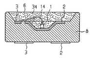
도 3에 도시된 실시예에서 제 1 및 제 2 전기 접속부(2, 3)는 리세스(9)를 갖는 그리고 경우에 따라 미리 제조된 광투과성 베이스 하우징(8) 내부에 매립된다. "미리 제조된"이란 표현은, 반도체 바디가 접속부(2)상에 조립되기 전에 미리 베이스 하우징(8)이 예를 들어 사출 성형에 의해서 접속부(2, 3)에 형성된다는 것을 의미한다. 베이스 하우징(8)은 예를 들어 광투과성 플라스틱으로 이루어지며, 리세스(9)는 형태면에서 볼 때 동작 동안에 (경우에 따라서는 리세스(9)의 내벽을 적절하게 코팅함으로써) 반도체 바디로부터 방출된 광선을 위한 리플렉터(17)로서 형성된다. 상기 베이스 하우징(8)은 특히 인쇄 회로 기판상에 표면 실장될 수 있 는 발광 다이오드에 사용된다. 베이스 하우징은 반도체 바디를 조립하기 전에 전기 접속부(2, 3)를 포함하는 리드 프레임상에 예를 들어 사출 성형에 의해서 제공된다.In the embodiment shown in FIG. 3, the first and second
리세스(9)는 발광 변환층(4), 예를 들어 별도로 제조되며 상기 베이스 하우징(8)상에 고정된, 플라스틱으로 이루어진 커버 플레이트(17)에 의해서 커버된다. 발광 변환층(4)에 적합한 재료로서는 재차 본 명세서의 기술분야에서 언급한 플라스틱 또는 무기 유리가 앞서 언급한 발광 물질과 함께 사용된다. 리세스(9)는 투과성 플라스틱, 무기 유리 또는 가스로 채워질 수 있을 뿐만 아니라 진공으로 형성될 수도 있다.The
도 2에 따른 실시예에서와 마찬가지로 본 실시예에서도 발광 변환층(4)으로부터 광을 더 우수하게 분리(decoupling)하기 위해서 상기 변환층상에 렌즈 형태의 (파선으로 도시된) 커버(29)가 제공될 수 있으며, 이 커버는 발광 변환층(4) 내부에서 광선의 전체 반사를 감소시킨다. 상기 커버(29)는 투과성 플라스틱으로 이루어질 수 있고, 발광 변환층(4) 상에 예를 들어 접착되거나 또는 발광 변환층(4)과 함께 일체로 형성될 수 있다.As in the embodiment according to FIG. 2, in this embodiment a cover 29 (shown in broken lines) in the form of a lens is provided on the conversion layer in order to better decoupling light from the light emitting
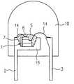
특히 바람직한 실시예에서는 도 10에서 보여지는 바와 같이 리세스(9)가 발광 물질을 포함하는 에폭시수지, 즉 발광 변환 소자를 형성하는 발광 커버링(5)으로 채워진다. 커버 플레이트(17) 및/또는 렌즈 형태의 커버(29)는 없을 수도 있다. 옵션으로서, 도 13에 도시된 바와 같이 제 1 전기 접속부(2)가 예를 들어 압형(embossing)에 의해 반도체 바디(1)의 영역에서 발광 변환 커버링(5)으로 채워진 리플렉터 웰(34)로 형성된다.In a particularly preferred embodiment, the
도 4에는 추가 실시예로서 소위 레이디얼 다이오드가 도시되어 있다. 본 실시예에서 반도체 바디(1)는 리플렉터로서 형성된 제 1 전기 접속부(2)의 일부분(16)에 예를 들어 납땜 또는 접착에 의해서 고정된다. 상기와 같은 하우징 구성 형태는 발광 다이오드 기술에서 공지되어 있기 때문에 더 이상 자세하게 설명하지 않겠다.4 shows a so-called radial diode as a further embodiment. In this embodiment, the
도 4의 실시예에서 반도체 바디(1)는 투과성 커버링(15)에 의해서 둘러싸여 있는데, 상기 커버링은 2번째로 언급한 실시예(도 2)에서와 마찬가지로 반도체 바디(1)로부터 방출된 광선의 파장 변동에 영향을 미치지 않으며, 예를 들어 발광 다이오드 기술에서 통상적으로 사용되는 투과성 에폭시수지 또는 무기 유리로 이루어질 수 있다.In the embodiment of FIG. 4, the
상기 투과성 커버링(15)상에는 발광 변환층(4)이 제공된다. 이 발광 변환층을 위한 재료로서는 예를 들어 재차 전술한 실시예와 관련하여 기술된 플라스틱 또는 무기 유리가 상기 실시예에 언급된 색소와 결합하여 사용된다.The light emitting
반도체 바디(1), 전기 접속부(2, 3)의 일부 영역, 투과성 커버링(15) 및 발광 변환층(4)으로 이루어진 전체 구성은, 발광 변환층(4)을 통과하는 광선의 파장 변동에 영향을 미치지 않는 추가의 투과성 커버링(10)에 의해서 직접 둘러싸인다. 상기 투과성 커버링은 재차 예를 들어 발광 다이오드 기술에서 통상적으로 사용되는 투과성 에폭시수지 또는 무기 유리로 이루어진다.The overall configuration of the
도 5에 도시된 실시예는, 반도체 바디(1)의 노출 표면이 발광 변환 커버링 (5)에 의해서 직접 커버되고, 상기 커버링은 재차 추가의 투과성 커버링(10)에 의해서 둘러싸인다는 점에서 실제로 도 4의 실시예와 상이하다. 도 5에는 또한 예를 들어 하부면 콘택 대신에 제 2본딩 와이어(14)를 통해서 관련 전기 접속부(2 또는 3)와 결합된 추가 콘택이 반도체 연속층(7)상에 제공된 반도체 바디(1)가 도시되어 있다. 물론 상기와 같은 반도체 바디(1)는 여기에 기술된 다른 모든 실시예에서도 사용될 수 있다. 그와 반대로, 전술한 실시예에 따른 반도체 바디(1)는 도 5의 실시예에서도 사용될 수 있다.In the embodiment shown in FIG. 5, in fact the exposed surface of the
완결성을 위하여, 물론 도 5에 따른 구조적 형상에서도 또한 도 1에 따른 실시예와 유사하게 일체형의 발광 변환 커버링(5)이 사용되는데, 상기 일체형의 발광 변환 커버링은 발광 변환 커버링(5)과 추가의 투과성 커버링(10)으로 이루어진 결합을 대체한다.For the sake of completeness, of course, also in the structural shape according to FIG. 5, an integrated light emitting conversion covering 5 is used similarly to the embodiment according to FIG. 1, wherein the integrated light emitting conversion covering 5 is combined with the light emitting conversion covering 5. Replaces the bond consisting of the
도 6에 따른 실시예에서 발광 변환층(4)(가능하다면 전술한 것과 같은 재료)은 직접 반도체 바디(1)상에 제공된다. 반도체 바디 및 전기 접속부(2, 3)의 일부 영역은 추가의 투과성 커버링(10)에 의해서 둘러싸이는데, 이 투과성 커버링은 발광 변환층(4)을 통과하는 광선의 파장 변동에 아무런 영향도 미치지 않으며, 예를 들어 발광 다이오드 기술에서 사용될 수 있는 투과성 에폭시수지 또는 유리로 제조된다.In the embodiment according to FIG. 6, the light emitting conversion layer 4 (possibly as described above) is provided directly on the
발광 변환층(4)이 제공된, 커버링이 없는 상기와 같은 반도체 바디(1)는 물론 바람직하게 발광 다이오드 기술로부터 공지된 전체적인 하우징의 구조적 형상(예컨대 SMD-하우징, 레이디얼-하우징(도 5와 비교))에서 사용될 수 있다.Such a
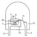
도 14에 도시된 본 발명에 따른 반도체 바디의 실시예에서 반도체 바디(1)상에는 투과성 웰부분(35)이 배치되어 있으며, 이 웰부분은 반도체 바디(1) 위에 하나의 웰(36)을 포함하고 있다. 상기 웰부분(35)은 예컨대 투과성 에폭시수지 또는 무기 유리로 이루어지고, 예를 들어 반도체 바디(1)를 포함한 전기 접속부(2, 3)의 사출 성형 커버링에 의해서 제조된다. 상기 웰(36) 내부에는, 예컨대 재차 에폭시수지 또는 무기 유리로 제조되며 전술한 무기 발광 물질로 이루어진 입자(6)에 결합된 발광 변환층(4)이 배치된다. 상기와 같은 구조적 형상에서는 바람직하게, 반도체 바디의 제조 동안 발광 물질을 예정되지 않은 장소, 예컨대 반도체 바디의 옆에 모으는 것이 간단한 방식으로 보장된다. 웰부분(35)은 물론 별도로 제조될 수도 있고, 또한 예를 들어 하우징부의 반도체 바디(1) 위에 고정될 수도 있다.In the embodiment of the semiconductor body according to the invention shown in FIG. 14, a
전술한 모든 실시예에서는 방출된 광의 색 효과를 최적화하기 위해서 그리고 방출 특성을 매칭시키기 위해서, 발광 변환 소자 (발광 변환 커버링(5) 또는 발광 변환층(4)), 경우에 따라서는 투과성 커버링(15), 및/또는 경우에 따라서는 추가의 투과성 커버링(10)이 광을 확산시키는 입자, 바람직하게는 소위 확산체를 포함한다. 상기와 같은 확산체의 예로서는 미네랄 충진제, 특히 CaF2, TiO2, SiO2, CaCO3 또는 BaSO4 혹은 유기 안료도 있다. 이러한 재료들은 간단한 방식으로 전술한 플라스틱에 첨가될 수 있다.In all the embodiments described above, in order to optimize the color effect of the emitted light and to match the emission characteristics, a light emitting conversion element (light emitting conversion covering 5 or light emitting conversion layer 4), in some cases transparent covering 15 ) And / or optionally the additional transmissive covering 10 comprises particles which diffuse light, preferably so-called diffusers. Examples of such diffusers are mineral fillers, in particular CaF2 , TiO2 , SiO2 , CaCO3 or BaSO4 or organic pigments. Such materials can be added to the plastics described above in a simple manner.
도 7, 8 및 도 12에는 청색광을 방출하는 반도체 바디의 방출 스펙트럼(도 7)(λ가 ≒ 430㎚ 일 때 발광 최대치) 또는 상기 반도체 바디를 이용하여 제조된 백색광을 방출하는 본 발명에 따른 반도체 소자의 방출 스펙트럼(도 8 및 도 12)이 도시되어 있다. 횡좌표에는 각각 파장(λ)이 ㎚로 그리고 종좌표상에는 각각 상대적 전자 발광(EL) 세기가 기입되어 있다.7, 8 and 12 show the emission spectrum of the semiconductor body emitting blue light (FIG. 7) (maximum emission when lambda is 430 nm) or a semiconductor according to the present invention emitting white light produced using the semiconductor body. The emission spectrum of the device (FIGS. 8 and 12) is shown. In the abscissa, the wavelength? Is in nm, and in the ordinate, the relative electroluminescence (EL) intensities are written, respectively.
반도체 바디로부터 방출된 도 7에 따른 광선으로부터 단지 일부분만이 더 긴 파장 영역으로 변환됨으로써, 혼합색으로서 백색광이 형성된다. 도 8의 파선(30)은 2개의 보색 파장 영역(청색 및 황색)으로 이루어진 광선 및 그에 의해 전체적으로 백색의 광을 방출하는 본 발명에 따른 반도체 소자의 방출 스펙트럼을 나타낸다. 이 경우 방출 스펙트럼은 약 400 내지 약 430 ㎚(청색)의 파장에서 그리고 약 550 내지 약 580㎚(황색)의 파장에서 각각 최대치를 갖는다. 실선(31)은 3개의 파장 영역(청색, 녹색 및 적색으로 이루어진 부가의 3색)을 혼합하여 백색을 만드는 본 발명에 따른 반도체 소자의 방출 스펙트럼을 보여준다. 상기 방출 스펙트럼은 예를 들어 약 430㎚(청색), 약 500㎚(녹색) 및 약 615㎚(적색)의 파장 영역에서 각각 최대치를 갖는다.Only a portion of the light beam according to FIG. 7 emitted from the semiconductor body is converted into a longer wavelength region, whereby white light is formed as a mixed color. The
도 11에는 또한 청색광(약 470㎚의 파장에서 최대치) 및 적색광(약 620㎚의 파장에서 최대치)으로 이루어진 혼색광을 방출하는 본 발명에 따른 반도체 소자의 방출 스펙트럼이 도시되어 있다. 사람의 눈에는 방출된 광의 전체 색 효과가 자홍색(magenta)이다. 반도체 바디로부터 방출된 방출 스펙트럼은 재차 도 7의 방출 스펙트럼과 일치한다.11 also shows the emission spectrum of the semiconductor device according to the invention which emits mixed color light consisting of blue light (maximum at a wavelength of about 470 nm) and red light (maximum at a wavelength of about 620 nm). In the human eye, the overall color effect of the emitted light is magenta. The emission spectrum emitted from the semiconductor body again coincides with the emission spectrum of FIG. 7.
도 12는, 도 7에 따른 방출 스펙트럼을 방출하는 반도체 바디를 포함하며 발광 물질로서 YAG:Ce가 사용되는 백색광을 발하는 본 발명에 따른 반도체 소자를 보여준다. 반도체 바디로부터 방출된 도 7에 따른 광선 중에서 단지 일부만이 더 긴 파장 영역으로 변환됨으로써, 혼합색으로서 백색광이 형성된다. 상이한 방식으로 표시된 도 12의 선(30 내지 33)은 발광 변환 소자, 본 경우에는 에폭시수지로 이루어진 발광 변환 커버링이 상이한 YAG:Ce 농도를 갖는 본 발명에 따른 반도체 소자의 방출 스펙트럼을 보여준다. 각각의 방출 스펙트럼은 λ = 420㎚ 내지 λ = 430㎚ 일 때, 즉 청색 스펙트럼 영역에서, 그리고 λ = 520㎚ 내지 λ = 545㎚일 때, 즉 녹색 스펙트럼 영역에서 각각 최대 세기를 가지며, 이 경우 더 긴 파장의 최대 세기를 갖는 방출 대역은 대부분 황색 스펙트럼 영역에 있다. 도 12의 다이아그램을 통해, 본 발명에 따른 반도체 소자에서는 간단한 방식으로 발광 물질 농도를 변동시킴으로써 에폭시수지 내에서의 백색광의 CIE-색 로커스가 변동될 수 있다는 것이 분명해진다.FIG. 12 shows a semiconductor device according to the invention comprising a semiconductor body that emits an emission spectrum according to FIG. 7 and emitting white light in which YAG: Ce is used as the light emitting material. Only a portion of the light rays according to FIG. 7 emitted from the semiconductor body are converted into longer wavelength regions, whereby white light is formed as a mixed color.
또한, 무기 발광 물질을 에폭시수지 또는 유리 내부로 분산시키지 않으면서, Ce 도핑된 그라네이트, 티오갈레이트, 알칼리토금속황화물 및 알루미네이트를 기재로 하는 무기 발광 물질을 직접 반도체 바디상에 제공할 수도 있다.It is also possible to provide an inorganic light emitting material based on Ce doped granate, thiogallate, alkaline earth metal sulfide and aluminate directly onto the semiconductor body without dispersing the inorganic light emitting material into the epoxy resin or glass. .
전술한 무기 발광 물질의 추가의 장점은, 예를 들어 에폭시수지내에서의 발광 물질의 농도가 유기 색소에서와 마찬가지로 용해성에 의해서 제한되지 않는다는 점이다. 그럼으로써, 두께가 큰 발광 변환 소자가 필요치 않게 된다.A further advantage of the above-mentioned inorganic light emitting material is that the concentration of the light emitting material in, for example, an epoxy resin is not limited by solubility as in organic pigments. This eliminates the need for a large light emitting conversion element.
전술한 실시예를 참조로 한 본 발명에 따른 반도체 소자의 설명은 당연히 본 발명을 상기 실시예에만 한정시키지 않는다. 예컨대 발광 다이오드 칩 또는 레이저 다이오드 칩과 같은 반도체 바디로서는 예를 들어 상응하는 광선 스펙트럼을 송출하는 중합체-LED도 포함될 수 있다.The description of the semiconductor device according to the present invention with reference to the above-described embodiment naturally does not limit the present invention to only the above-described embodiment. Semiconductor bodies such as, for example, light emitting diode chips or laser diode chips may also include, for example, polymer-LEDs which emit a corresponding light spectrum.
본 발명은 균일한 혼색광을 방출하고 가급적 재현가능한 소자 특성을 가짐으로써 기술적으로 간단한 대량 생산이 가능한 반도체 소자를 제공한다.The present invention provides a semiconductor device capable of technically simple mass production by emitting uniform mixed light and having reproducible device characteristics wherever possible.
Claims (22)
Translated fromKoreanApplications Claiming Priority (5)
| Application Number | Priority Date | Filing Date | Title |
|---|---|---|---|
| DE19625622.4 | 1996-06-26 | ||
| DE19625622ADE19625622A1 (en) | 1996-06-26 | 1996-06-26 | Light radiating semiconductor constructional element |
| DE19638667.5 | 1996-09-20 | ||
| DE19638667ADE19638667C2 (en) | 1996-09-20 | 1996-09-20 | Mixed-color light-emitting semiconductor component with luminescence conversion element |
| KR1019980710985AKR100537349B1 (en) | 1996-06-26 | 1997-06-26 | Light-emitting semiconductor component with luminescence conversion element |
Related Parent Applications (1)
| Application Number | Title | Priority Date | Filing Date |
|---|---|---|---|
| KR1019980710985ADivisionKR100537349B1 (en) | 1996-06-26 | 1997-06-26 | Light-emitting semiconductor component with luminescence conversion element |
Publications (2)
| Publication Number | Publication Date |
|---|---|
| KR20040111700A KR20040111700A (en) | 2004-12-31 |
| KR100702740B1true KR100702740B1 (en) | 2007-04-03 |
Family
ID=26026958
Family Applications (11)
| Application Number | Title | Priority Date | Filing Date |
|---|---|---|---|
| KR1019980710985AExpired - LifetimeKR100537349B1 (en) | 1996-06-26 | 1997-06-26 | Light-emitting semiconductor component with luminescence conversion element |
| KR1020047019070AExpired - LifetimeKR100702740B1 (en) | 1996-06-26 | 1997-06-26 | Light emitting semiconductor device including light emitting conversion device |
| KR1020057009021ACeasedKR20050053798A (en) | 1996-06-26 | 1997-06-26 | Light-emitting semiconductor component with luminescence conversion element |
| KR1020067012235AExpired - LifetimeKR100751692B1 (en) | 1996-06-26 | 1997-06-26 | Light-emitting semiconductor component with luminescence conversion element |
| KR1020067012234AExpired - LifetimeKR100808749B1 (en) | 1996-06-26 | 1997-06-26 | Light-emitting semiconductor component with luminescence conversion element |
| KR1020047019068AExpired - LifetimeKR100662955B1 (en) | 1996-06-26 | 1997-06-26 | Light emitting semiconductor device including light emitting conversion device |
| KR1020047019066AExpired - LifetimeKR100662956B1 (en) | 1996-06-26 | 1997-06-26 | Light emitting semiconductor device including light emitting conversion device |
| KR1020057009020AExpired - LifetimeKR100629544B1 (en) | 1996-06-26 | 1997-06-26 | Light-emitting semiconductor component with luminescence conversion element |
| KR1020047019069AExpired - Fee RelatedKR100734122B1 (en) | 1996-06-26 | 1997-06-26 | Light emitting semiconductor device including light emitting conversion device |
| KR20047019071ACeasedKR20040111701A (en) | 1996-06-26 | 1997-06-26 | Light-emitting semiconductor component with luminescence conversion element |
| KR1020047019067AExpired - LifetimeKR100643442B1 (en) | 1996-06-26 | 1997-06-26 | Light emitting semiconductor device including light emitting conversion device |
Family Applications Before (1)
| Application Number | Title | Priority Date | Filing Date |
|---|---|---|---|
| KR1019980710985AExpired - LifetimeKR100537349B1 (en) | 1996-06-26 | 1997-06-26 | Light-emitting semiconductor component with luminescence conversion element |
Family Applications After (9)
| Application Number | Title | Priority Date | Filing Date |
|---|---|---|---|
| KR1020057009021ACeasedKR20050053798A (en) | 1996-06-26 | 1997-06-26 | Light-emitting semiconductor component with luminescence conversion element |
| KR1020067012235AExpired - LifetimeKR100751692B1 (en) | 1996-06-26 | 1997-06-26 | Light-emitting semiconductor component with luminescence conversion element |
| KR1020067012234AExpired - LifetimeKR100808749B1 (en) | 1996-06-26 | 1997-06-26 | Light-emitting semiconductor component with luminescence conversion element |
| KR1020047019068AExpired - LifetimeKR100662955B1 (en) | 1996-06-26 | 1997-06-26 | Light emitting semiconductor device including light emitting conversion device |
| KR1020047019066AExpired - LifetimeKR100662956B1 (en) | 1996-06-26 | 1997-06-26 | Light emitting semiconductor device including light emitting conversion device |
| KR1020057009020AExpired - LifetimeKR100629544B1 (en) | 1996-06-26 | 1997-06-26 | Light-emitting semiconductor component with luminescence conversion element |
| KR1020047019069AExpired - Fee RelatedKR100734122B1 (en) | 1996-06-26 | 1997-06-26 | Light emitting semiconductor device including light emitting conversion device |
| KR20047019071ACeasedKR20040111701A (en) | 1996-06-26 | 1997-06-26 | Light-emitting semiconductor component with luminescence conversion element |
| KR1020047019067AExpired - LifetimeKR100643442B1 (en) | 1996-06-26 | 1997-06-26 | Light emitting semiconductor device including light emitting conversion device |
Country Status (8)
| Country | Link |
|---|---|
| US (10) | US7078732B1 (en) |
| EP (12) | EP1441397B1 (en) |
| JP (10) | JP3773541B2 (en) |
| KR (11) | KR100537349B1 (en) |
| CN (3) | CN1534802B (en) |
| BR (2) | BR9709998B1 (en) |
| DE (6) | DE59711671D1 (en) |
| WO (1) | WO1997050132A1 (en) |
Families Citing this family (773)
| Publication number | Priority date | Publication date | Assignee | Title |
|---|---|---|---|---|
| US6600175B1 (en) | 1996-03-26 | 2003-07-29 | Advanced Technology Materials, Inc. | Solid state white light emitter and display using same |
| US20040239243A1 (en)* | 1996-06-13 | 2004-12-02 | Roberts John K. | Light emitting assembly |
| KR100537349B1 (en) | 1996-06-26 | 2006-02-28 | 오스람 게젤샤프트 미트 베쉬랭크터 하프퉁 | Light-emitting semiconductor component with luminescence conversion element |
| DE19638667C2 (en) | 1996-09-20 | 2001-05-17 | Osram Opto Semiconductors Gmbh | Mixed-color light-emitting semiconductor component with luminescence conversion element |
| AU744210B2 (en)* | 1996-07-29 | 2002-02-21 | Nichia Corporation | Light emitting device and display |
| TW383508B (en)* | 1996-07-29 | 2000-03-01 | Nichia Kagaku Kogyo Kk | Light emitting device and display |
| DE19645035C1 (en)* | 1996-10-31 | 1998-04-30 | Siemens Ag | Multi-color light emitting image display device |
| US5895932A (en)* | 1997-01-24 | 1999-04-20 | International Business Machines Corporation | Hybrid organic-inorganic semiconductor light emitting diodes |
| JP3378465B2 (en)* | 1997-05-16 | 2003-02-17 | 株式会社東芝 | Light emitting device |
| EP0883195A1 (en)* | 1997-06-03 | 1998-12-09 | BARR & STROUD LIMITED | Head tracking system comprising LED with fluorescent coating |
| JP4271747B2 (en)* | 1997-07-07 | 2009-06-03 | 株式会社朝日ラバー | Translucent coating material for light emitting diode and fluorescent color light source |
| US6319425B1 (en) | 1997-07-07 | 2001-11-20 | Asahi Rubber Inc. | Transparent coating member for light-emitting diodes and a fluorescent color light source |
| US6623670B2 (en) | 1997-07-07 | 2003-09-23 | Asahi Rubber Inc. | Method of molding a transparent coating member for light-emitting diodes |
| US5847507A (en)* | 1997-07-14 | 1998-12-08 | Hewlett-Packard Company | Fluorescent dye added to epoxy of light emitting diode lens |
| CN1142598C (en) | 1997-07-25 | 2004-03-17 | 日亚化学工业株式会社 | Nitride semiconductor light emitting device |
| US7038398B1 (en) | 1997-08-26 | 2006-05-02 | Color Kinetics, Incorporated | Kinetic illumination system and methods |
| US7161313B2 (en)* | 1997-08-26 | 2007-01-09 | Color Kinetics Incorporated | Light emitting diode based products |
| US6806659B1 (en) | 1997-08-26 | 2004-10-19 | Color Kinetics, Incorporated | Multicolored LED lighting method and apparatus |
| US20030133292A1 (en)* | 1999-11-18 | 2003-07-17 | Mueller George G. | Methods and apparatus for generating and modulating white light illumination conditions |
| US7014336B1 (en) | 1999-11-18 | 2006-03-21 | Color Kinetics Incorporated | Systems and methods for generating and modulating illumination conditions |
| US6340824B1 (en)* | 1997-09-01 | 2002-01-22 | Kabushiki Kaisha Toshiba | Semiconductor light emitting device including a fluorescent material |
| DE19755734A1 (en)* | 1997-12-15 | 1999-06-24 | Siemens Ag | Method for producing a surface-mountable optoelectronic component |
| US7598686B2 (en) | 1997-12-17 | 2009-10-06 | Philips Solid-State Lighting Solutions, Inc. | Organic light emitting diode methods and apparatus |
| US6252254B1 (en) | 1998-02-06 | 2001-06-26 | General Electric Company | Light emitting device with phosphor composition |
| US6580097B1 (en)* | 1998-02-06 | 2003-06-17 | General Electric Company | Light emitting device with phosphor composition |
| US6152590A (en) | 1998-02-13 | 2000-11-28 | Donnelly Hohe Gmbh & Co. Kg | Lighting device for motor vehicles |
| US6501091B1 (en)* | 1998-04-01 | 2002-12-31 | Massachusetts Institute Of Technology | Quantum dot white and colored light emitting diodes |
| FR2779694B1 (en)* | 1998-06-10 | 2000-08-11 | Sagem | POLYCHROME LIGHTED DASHBOARD |
| US5959316A (en)* | 1998-09-01 | 1999-09-28 | Hewlett-Packard Company | Multiple encapsulation of phosphor-LED devices |
| KR100702273B1 (en)† | 1998-09-28 | 2007-03-30 | 코닌클리즈케 필립스 일렉트로닉스 엔.브이. | Lighting system |
| US6429583B1 (en) | 1998-11-30 | 2002-08-06 | General Electric Company | Light emitting device with ba2mgsi2o7:eu2+, ba2sio4:eu2+, or (srxcay ba1-x-y)(a1zga1-z)2sr:eu2+phosphors |
| JP2000208822A (en) | 1999-01-11 | 2000-07-28 | Matsushita Electronics Industry Corp | Semiconductor light emitting device |
| DE19902750A1 (en) | 1999-01-25 | 2000-08-03 | Osram Opto Semiconductors Gmbh | Semiconductor component for generating mixed-colored electromagnetic radiation |
| US6683325B2 (en)* | 1999-01-26 | 2004-01-27 | Patent-Treuhand-Gesellschaft-für Elektrische Glühlampen mbH | Thermal expansion compensated opto-electronic semiconductor element, particularly ultraviolet (UV) light emitting diode, and method of its manufacture |
| JP2000223749A (en)* | 1999-01-29 | 2000-08-11 | Seiwa Electric Mfg Co Ltd | Light emitting diode lamp, method for manufacturing the same, chip type light emitting diode element and dot matrix type light emitting diode unit |
| JP3770014B2 (en) | 1999-02-09 | 2006-04-26 | 日亜化学工業株式会社 | Nitride semiconductor device |
| US6351069B1 (en)* | 1999-02-18 | 2002-02-26 | Lumileds Lighting, U.S., Llc | Red-deficiency-compensating phosphor LED |
| ATE452445T1 (en) | 1999-03-04 | 2010-01-15 | Nichia Corp | NITRIDE SEMICONDUCTOR LASER ELEMENT |
| US6528234B1 (en)* | 1999-03-05 | 2003-03-04 | The United States Of America As Represented By The Secretary Of The Navy | II-VI compounds as a medium for optical data storage through fast persistent high density spectral holeburning |
| US6514435B1 (en)* | 1999-03-05 | 2003-02-04 | The United States Of America As Represented By The Secretary Of The Navy | High density and fast persistent spectral holeburning in II-VI compounds for optical data storage |
| DE19922361C2 (en) | 1999-05-14 | 2003-05-28 | Osram Opto Semiconductors Gmbh | LED module for display devices |
| US6489637B1 (en)* | 1999-06-09 | 2002-12-03 | Sanyo Electric Co., Ltd. | Hybrid integrated circuit device |
| EP1116419B1 (en) | 1999-07-23 | 2004-10-06 | Osram Opto Semiconductors GmbH | Luminescent array, wavelength-converting sealing material and light source |
| WO2001008452A1 (en) | 1999-07-23 | 2001-02-01 | Patent-Treuhand-Gesellschaft für elektrische Glühlampen mbH | Luminous substance for a light source and light source associated therewith |
| DE29914037U1 (en)* | 1999-08-11 | 2000-12-28 | Diehl AKO Stiftung GmbH & Co. KG, 88239 Wangen | Indoor lighting for household appliances |
| US6504301B1 (en)* | 1999-09-03 | 2003-01-07 | Lumileds Lighting, U.S., Llc | Non-incandescent lightbulb package using light emitting diodes |
| US6696703B2 (en) | 1999-09-27 | 2004-02-24 | Lumileds Lighting U.S., Llc | Thin film phosphor-converted light emitting diode device |
| KR100683364B1 (en) | 1999-09-27 | 2007-02-15 | 필립스 루미리즈 라이팅 캄파니 엘엘씨 | Light Emitting Diodes Generate White Light by Complete Fluorescence Conversion |
| US6686691B1 (en) | 1999-09-27 | 2004-02-03 | Lumileds Lighting, U.S., Llc | Tri-color, white light LED lamps |
| US20020176259A1 (en) | 1999-11-18 | 2002-11-28 | Ducharme Alfred D. | Systems and methods for converting illumination |
| US7202506B1 (en) | 1999-11-19 | 2007-04-10 | Cree, Inc. | Multi element, multi color solid state LED/laser |
| US8829546B2 (en) | 1999-11-19 | 2014-09-09 | Cree, Inc. | Rare earth doped layer or substrate for light conversion |
| US6513949B1 (en) | 1999-12-02 | 2003-02-04 | Koninklijke Philips Electronics N.V. | LED/phosphor-LED hybrid lighting systems |
| DE19963805B4 (en) | 1999-12-30 | 2005-01-27 | Osram Opto Semiconductors Gmbh | White light source based on non-linear optical processes |
| DE19964252A1 (en) | 1999-12-30 | 2002-06-06 | Osram Opto Semiconductors Gmbh | Surface mount component for an LED white light source |
| DE10010638A1 (en)* | 2000-03-03 | 2001-09-13 | Osram Opto Semiconductors Gmbh | Making light emitting semiconducting body with luminescence conversion element involves applying suspension with solvent, adhesive, luminescent material |
| US6522065B1 (en)* | 2000-03-27 | 2003-02-18 | General Electric Company | Single phosphor for creating white light with high luminosity and high CRI in a UV led device |
| US6867542B1 (en)* | 2000-03-29 | 2005-03-15 | General Electric Company | Floating chip photonic device and method of manufacture |
| US6603258B1 (en)* | 2000-04-24 | 2003-08-05 | Lumileds Lighting, U.S. Llc | Light emitting diode device that emits white light |
| DE10020465A1 (en) | 2000-04-26 | 2001-11-08 | Osram Opto Semiconductors Gmbh | Radiation-emitting semiconductor component with luminescence conversion element |
| DE10023353A1 (en)* | 2000-05-12 | 2001-11-29 | Osram Opto Semiconductors Gmbh | Optoelectronic component and method for producing it |
| US6501100B1 (en)* | 2000-05-15 | 2002-12-31 | General Electric Company | White light emitting phosphor blend for LED devices |
| JP4066620B2 (en)* | 2000-07-21 | 2008-03-26 | 日亜化学工業株式会社 | LIGHT EMITTING ELEMENT, DISPLAY DEVICE HAVING LIGHT EMITTING ELEMENT AND METHOD FOR MANUFACTURING DISPLAY DEVICE |
| JP2002050797A (en) | 2000-07-31 | 2002-02-15 | Toshiba Corp | Semiconductor-excited phosphor light emitting device and method of manufacturing the same |
| JP2002141556A (en) | 2000-09-12 | 2002-05-17 | Lumileds Lighting Us Llc | Light-emitting diode with improved light extraction effect |
| JP3609709B2 (en)* | 2000-09-29 | 2005-01-12 | 株式会社シチズン電子 | Light emitting diode |
| US6650044B1 (en)* | 2000-10-13 | 2003-11-18 | Lumileds Lighting U.S., Llc | Stenciling phosphor layers on light emitting diodes |
| JP3614776B2 (en)* | 2000-12-19 | 2005-01-26 | シャープ株式会社 | Chip component type LED and its manufacturing method |
| US6800870B2 (en)* | 2000-12-20 | 2004-10-05 | Michel Sayag | Light stimulating and collecting methods and apparatus for storage-phosphor image plates |
| US20020079505A1 (en)* | 2000-12-21 | 2002-06-27 | Stefan Becker | Semiconductor light unit and method for production of the same |
| JP2002195858A (en)* | 2000-12-27 | 2002-07-10 | Nippon Seiki Co Ltd | Display |
| DE10065381B4 (en)* | 2000-12-27 | 2010-08-26 | Osram Opto Semiconductors Gmbh | Radiation-emitting semiconductor component with luminescence conversion element |
| AT410266B (en) | 2000-12-28 | 2003-03-25 | Tridonic Optoelectronics Gmbh | LIGHT SOURCE WITH A LIGHT-EMITTING ELEMENT |
| US6930737B2 (en)* | 2001-01-16 | 2005-08-16 | Visteon Global Technologies, Inc. | LED backlighting system |
| MY145695A (en) | 2001-01-24 | 2012-03-30 | Nichia Corp | Light emitting diode, optical semiconductor device, epoxy resin composition suited for optical semiconductor device, and method for manufacturing the same |
| JP2002232013A (en)* | 2001-02-02 | 2002-08-16 | Rohm Co Ltd | Semiconductor light emitting device |
| DE10105802A1 (en) | 2001-02-07 | 2002-08-08 | Patent Treuhand Ges Fuer Elektrische Gluehlampen Mbh | Semiconductor component with reflector |
| DE10109349B4 (en)* | 2001-02-27 | 2012-04-19 | Osram Opto Semiconductors Gmbh | Radiation-emitting semiconductor component |
| US6417019B1 (en)* | 2001-04-04 | 2002-07-09 | Lumileds Lighting, U.S., Llc | Phosphor converted light emitting diode |
| US6949771B2 (en)* | 2001-04-25 | 2005-09-27 | Agilent Technologies, Inc. | Light source |
| US6598998B2 (en)* | 2001-05-04 | 2003-07-29 | Lumileds Lighting, U.S., Llc | Side emitting light emitting device |
| US6989412B2 (en) | 2001-06-06 | 2006-01-24 | Henkel Corporation | Epoxy molding compounds containing phosphor and process for preparing such compositions |
| US6576488B2 (en) | 2001-06-11 | 2003-06-10 | Lumileds Lighting U.S., Llc | Using electrophoresis to produce a conformally coated phosphor-converted light emitting semiconductor |
| US6642652B2 (en) | 2001-06-11 | 2003-11-04 | Lumileds Lighting U.S., Llc | Phosphor-converted light emitting device |
| JP4789350B2 (en)* | 2001-06-11 | 2011-10-12 | シチズン電子株式会社 | Manufacturing method of light emitting diode |
| US6664560B2 (en)* | 2001-06-15 | 2003-12-16 | Cree, Inc. | Ultraviolet light emitting diode |
| DE10131698A1 (en)* | 2001-06-29 | 2003-01-30 | Osram Opto Semiconductors Gmbh | Surface-mountable radiation-emitting component and method for its production |
| TW552726B (en)* | 2001-07-26 | 2003-09-11 | Matsushita Electric Works Ltd | Light emitting device in use of LED |
| DE10137641A1 (en)* | 2001-08-03 | 2003-02-20 | Osram Opto Semiconductors Gmbh | Hybrid LED |
| JP3948650B2 (en) | 2001-10-09 | 2007-07-25 | アバゴ・テクノロジーズ・イーシービーユー・アイピー(シンガポール)プライベート・リミテッド | Light emitting diode and manufacturing method thereof |
| DE10153259A1 (en)* | 2001-10-31 | 2003-05-22 | Osram Opto Semiconductors Gmbh | Optoelectronic component |
| JP2003152227A (en)* | 2001-11-14 | 2003-05-23 | Citizen Electronics Co Ltd | LED color correction means and color correction method |
| JP3768864B2 (en)* | 2001-11-26 | 2006-04-19 | シチズン電子株式会社 | Surface mount type light emitting diode and manufacturing method thereof |
| US6836502B2 (en) | 2002-01-17 | 2004-12-28 | Hutchinson Technology Incorporated | Spectroscopy light source |
| US6734466B2 (en)* | 2002-03-05 | 2004-05-11 | Agilent Technologies, Inc. | Coated phosphor filler and a method of forming the coated phosphor filler |
| US6943379B2 (en)* | 2002-04-04 | 2005-09-13 | Toyoda Gosei Co., Ltd. | Light emitting diode |
| KR100632659B1 (en)* | 2002-05-31 | 2006-10-11 | 서울반도체 주식회사 | White light emitting diode |
| CA2489237A1 (en)* | 2002-06-13 | 2003-12-24 | Cree, Inc. | Semiconductor emitter comprising a saturated phosphor |
| US6841802B2 (en) | 2002-06-26 | 2005-01-11 | Oriol, Inc. | Thin film light emitting diode |
| US7088040B1 (en)* | 2002-06-27 | 2006-08-08 | University Of Central Florida Research Foundation, Inc. | Light source using emitting particles to provide visible light |
| KR101030068B1 (en)* | 2002-07-08 | 2011-04-19 | 니치아 카가쿠 고교 가부시키가이샤 | Nitride semiconductor device manufacturing method and nitride semiconductor device |
| JP2004047748A (en)* | 2002-07-12 | 2004-02-12 | Stanley Electric Co Ltd | Light emitting diode |
| US7928455B2 (en)* | 2002-07-15 | 2011-04-19 | Epistar Corporation | Semiconductor light-emitting device and method for forming the same |
| WO2004017407A1 (en) | 2002-07-31 | 2004-02-26 | Osram Opto Semiconductors Gmbh | Surface-mounted semiconductor component and method for the production thereof |
| JP4360788B2 (en)* | 2002-08-29 | 2009-11-11 | シチズン電子株式会社 | Backlight for liquid crystal display panel and method of manufacturing light emitting diode used therefor |
| US7800121B2 (en) | 2002-08-30 | 2010-09-21 | Lumination Llc | Light emitting diode component |
| CN100468791C (en)* | 2002-08-30 | 2009-03-11 | 吉尔科有限公司 | Light emitting diode with improved effience |
| US7224000B2 (en)* | 2002-08-30 | 2007-05-29 | Lumination, Llc | Light emitting diode component |
| US10340424B2 (en) | 2002-08-30 | 2019-07-02 | GE Lighting Solutions, LLC | Light emitting diode component |
| US20050218781A1 (en)* | 2002-09-09 | 2005-10-06 | Hsing Chen | Triple wavelengths light emitting diode |
| JP4201167B2 (en)* | 2002-09-26 | 2008-12-24 | シチズン電子株式会社 | Manufacturing method of white light emitting device |
| US6822991B2 (en)* | 2002-09-30 | 2004-11-23 | Lumileds Lighting U.S., Llc | Light emitting devices including tunnel junctions |
| US7592636B2 (en)* | 2002-09-30 | 2009-09-22 | Osram Opto Semiconductors Gmbh | Radiation-emitting semiconductor component and method for the production thereof |
| JP2004128273A (en) | 2002-10-03 | 2004-04-22 | Sharp Corp | Light emitting element |
| JP4280050B2 (en) | 2002-10-07 | 2009-06-17 | シチズン電子株式会社 | White light emitting device |
| AU2003278009A1 (en)* | 2002-10-18 | 2004-05-04 | Ifire Technology Inc. | Color electroluminescent displays |
| US20060003477A1 (en) | 2002-10-30 | 2006-01-05 | Bert Braune | Method for producing a light source provided with electroluminescent diodes and comprising a luminescence conversion element |
| DE10258193B4 (en)* | 2002-12-12 | 2014-04-10 | Osram Opto Semiconductors Gmbh | Method for producing light-emitting diode light sources with luminescence conversion element |
| WO2004059750A1 (en)* | 2002-12-25 | 2004-07-15 | Japan Science And Technology Agency | Light emitting element device, light receiving element device, optical apparatus, fluoride crystal, process for producing fluoride crystal and crucible |
| DE10261428B8 (en)* | 2002-12-30 | 2012-09-20 | Osram Opto Semiconductors Gmbh | Radiation-emitting semiconductor component with multiple luminescence conversion elements |
| DE10261672B4 (en)* | 2002-12-31 | 2005-11-24 | Osram Opto Semiconductors Gmbh | LED chip with conversion substance, optoelectronic component with such an LED chip and method for producing such an LED chip |
| TWI351548B (en) | 2003-01-15 | 2011-11-01 | Semiconductor Energy Lab | Manufacturing method of liquid crystal display dev |
| US7042020B2 (en) | 2003-02-14 | 2006-05-09 | Cree, Inc. | Light emitting device incorporating a luminescent material |
| US7423296B2 (en)* | 2003-02-26 | 2008-09-09 | Avago Technologies Ecbu Ip Pte Ltd | Apparatus for producing a spectrally-shifted light output from a light emitting device utilizing thin-film luminescent layers |
| KR20050113200A (en)* | 2003-02-26 | 2005-12-01 | 크리, 인코포레이티드 | Composite white light source and method for fabricating |
| JP4131178B2 (en)* | 2003-02-28 | 2008-08-13 | 豊田合成株式会社 | Light emitting device |
| DE10308866A1 (en) | 2003-02-28 | 2004-09-09 | Osram Opto Semiconductors Gmbh | Lighting module and method for its production |
| US20040173808A1 (en)* | 2003-03-07 | 2004-09-09 | Bor-Jen Wu | Flip-chip like light emitting device package |
| CN101789482B (en)* | 2003-03-10 | 2013-04-17 | 丰田合成株式会社 | Solid element device and method for manufacture thereof |
| US7038370B2 (en)* | 2003-03-17 | 2006-05-02 | Lumileds Lighting, U.S., Llc | Phosphor converted light emitting device |
| US7279832B2 (en)* | 2003-04-01 | 2007-10-09 | Innovalight, Inc. | Phosphor materials and illumination devices made therefrom |
| US20040252488A1 (en)* | 2003-04-01 | 2004-12-16 | Innovalight | Light-emitting ceiling tile |
| DE10316769A1 (en)* | 2003-04-10 | 2004-10-28 | Patent-Treuhand-Gesellschaft für elektrische Glühlampen mbH | Luminescence conversion LED used in optical semiconductor components has LED chip emitting primary radiation in specified region which is partially or completely converted into longer wavelength radiation |
| JP3931916B2 (en)* | 2003-04-24 | 2007-06-20 | 日亜化学工業株式会社 | Semiconductor device and manufacturing method thereof |
| CA2523544A1 (en)* | 2003-04-30 | 2004-11-18 | Cree, Inc. | High powered light emitter packages with compact optics |
| US7005679B2 (en) | 2003-05-01 | 2006-02-28 | Cree, Inc. | Multiple component solid state white light |
| US7777235B2 (en) | 2003-05-05 | 2010-08-17 | Lighting Science Group Corporation | Light emitting diodes with improved light collimation |
| US7157745B2 (en) | 2004-04-09 | 2007-01-02 | Blonder Greg E | Illumination devices comprising white light emitting diodes and diode arrays and method and apparatus for making them |
| US7633093B2 (en) | 2003-05-05 | 2009-12-15 | Lighting Science Group Corporation | Method of making optical light engines with elevated LEDs and resulting product |
| US7528421B2 (en) | 2003-05-05 | 2009-05-05 | Lamina Lighting, Inc. | Surface mountable light emitting diode assemblies packaged for high temperature operation |
| US7040774B2 (en)* | 2003-05-23 | 2006-05-09 | Goldeneye, Inc. | Illumination systems utilizing multiple wavelength light recycling |
| JP4138586B2 (en)* | 2003-06-13 | 2008-08-27 | スタンレー電気株式会社 | LED lamp for light source and vehicle headlamp using the same |
| CN100511732C (en) | 2003-06-18 | 2009-07-08 | 丰田合成株式会社 | Light emitting device |
| AT412928B (en)* | 2003-06-18 | 2005-08-25 | Guenther Dipl Ing Dr Leising | METHOD FOR PRODUCING A WHITE LED AND WHITE LED LIGHT SOURCE |
| JP4024721B2 (en)* | 2003-06-20 | 2007-12-19 | 株式会社小糸製作所 | Vehicle lamp and light source module |
| US7521667B2 (en) | 2003-06-23 | 2009-04-21 | Advanced Optical Technologies, Llc | Intelligent solid state lighting |
| US7145125B2 (en) | 2003-06-23 | 2006-12-05 | Advanced Optical Technologies, Llc | Integrating chamber cone light using LED sources |
| JP2005026688A (en)* | 2003-06-30 | 2005-01-27 | Osram Opto Semiconductors Gmbh | Radiation emitting semiconductor chip, method for manufacturing the semiconductor chip, and method for adjusting and setting the brightness of the semiconductor chip |
| US8999736B2 (en)* | 2003-07-04 | 2015-04-07 | Epistar Corporation | Optoelectronic system |
| US20050006659A1 (en)* | 2003-07-09 | 2005-01-13 | Ng Kee Yean | Light emitting diode utilizing a discrete wavelength-converting layer for color conversion |
| JP4200849B2 (en)* | 2003-07-17 | 2008-12-24 | 日産自動車株式会社 | Infrared projector for vehicles |
| DE102004034166B4 (en)* | 2003-07-17 | 2015-08-20 | Toyoda Gosei Co., Ltd. | Light-emitting device |
| JP4238666B2 (en)* | 2003-07-17 | 2009-03-18 | 豊田合成株式会社 | Method for manufacturing light emitting device |
| JP2005064233A (en)* | 2003-08-12 | 2005-03-10 | Stanley Electric Co Ltd | Wavelength conversion type LED |
| EP1659335A4 (en)* | 2003-08-28 | 2010-05-05 | Mitsubishi Chem Corp | LIGHT EMITTING DEVICE AND PHOSPHORUS |
| EP1515368B1 (en)* | 2003-09-05 | 2019-12-25 | Nichia Corporation | Light equipment |
| US7029935B2 (en)* | 2003-09-09 | 2006-04-18 | Cree, Inc. | Transmissive optical elements including transparent plastic shell having a phosphor dispersed therein, and methods of fabricating same |
| JP4140042B2 (en)* | 2003-09-17 | 2008-08-27 | スタンレー電気株式会社 | LED light source device using phosphor and vehicle headlamp using LED light source device |
| JP2005093712A (en)* | 2003-09-17 | 2005-04-07 | Stanley Electric Co Ltd | Semiconductor light emitting device |
| US7915085B2 (en) | 2003-09-18 | 2011-03-29 | Cree, Inc. | Molded chip fabrication method |
| JP4402425B2 (en)* | 2003-10-24 | 2010-01-20 | スタンレー電気株式会社 | Vehicle headlamp |
| US6933535B2 (en)* | 2003-10-31 | 2005-08-23 | Lumileds Lighting U.S., Llc | Light emitting devices with enhanced luminous efficiency |
| DE10351397A1 (en)* | 2003-10-31 | 2005-06-16 | Osram Opto Semiconductors Gmbh | LED chip |
| DE10351349A1 (en)* | 2003-10-31 | 2005-06-16 | Osram Opto Semiconductors Gmbh | Production of a luminescent diode chip applies a radiation decoupling surface and a semiconductor body with an epitaxial-grown sequence of semiconductor layers with an active zone |
| US20050099808A1 (en)* | 2003-11-12 | 2005-05-12 | Cheng Tzu C. | Light-emitting device |
| CN100377370C (en)* | 2003-11-22 | 2008-03-26 | 鸿富锦精密工业(深圳)有限公司 | Light-emitting diode and surface light source device |
| JP4385741B2 (en)* | 2003-11-25 | 2009-12-16 | パナソニック電工株式会社 | Light emitting device |
| US7518158B2 (en) | 2003-12-09 | 2009-04-14 | Cree, Inc. | Semiconductor light emitting devices and submounts |
| JP2005191420A (en)* | 2003-12-26 | 2005-07-14 | Stanley Electric Co Ltd | Semiconductor light emitting device having wavelength conversion layer and manufacturing method thereof |
| DE10361650A1 (en)* | 2003-12-30 | 2005-08-04 | Osram Opto Semiconductors Gmbh | Optoelectronic module and method for its production |
| JP2005197329A (en)* | 2004-01-05 | 2005-07-21 | Stanley Electric Co Ltd | Surface mount semiconductor device and lead frame structure thereof |
| US7183588B2 (en)* | 2004-01-08 | 2007-02-27 | Avago Technologies Ecbu Ip (Singapore) Pte. Ltd. | Light emission device |
| DE102004003928B4 (en)* | 2004-01-26 | 2012-02-23 | Tay Kheng Chiong | A miniaturized SM-technology optoelectronic device and method of making this device |
| US7250715B2 (en)* | 2004-02-23 | 2007-07-31 | Philips Lumileds Lighting Company, Llc | Wavelength converted semiconductor light emitting devices |
| DE102004029412A1 (en)* | 2004-02-27 | 2005-10-13 | Osram Opto Semiconductors Gmbh | Radiation-emitting semiconductor chip and method for producing such a semiconductor chip |
| JP2005244075A (en)* | 2004-02-27 | 2005-09-08 | Matsushita Electric Works Ltd | Light emitting device |
| JP2005286312A (en) | 2004-03-02 | 2005-10-13 | Fujikura Ltd | LIGHT EMITTING DEVICE AND LIGHTING DEVICE |
| US7573072B2 (en)* | 2004-03-10 | 2009-08-11 | Lumination Llc | Phosphor and blends thereof for use in LEDs |
| US7239080B2 (en)* | 2004-03-11 | 2007-07-03 | Avago Technologies Ecbu Ip (Singapore) Pte. Ltd | LED display with overlay |
| KR20050092300A (en)* | 2004-03-15 | 2005-09-21 | 삼성전기주식회사 | High power led package |
| US20050199990A1 (en)* | 2004-03-15 | 2005-09-15 | Intersil Americas Inc. | Protection of plastic detector's packages against shortwave light destruction |
| DE102004013680A1 (en)* | 2004-03-18 | 2005-10-20 | Siemens Ag | Light source for imaging unit |
| JP4504056B2 (en) | 2004-03-22 | 2010-07-14 | スタンレー電気株式会社 | Manufacturing method of semiconductor light emitting device |
| TWI286393B (en)* | 2004-03-24 | 2007-09-01 | Toshiba Lighting & Technology | Lighting apparatus |
| JP2005285925A (en)* | 2004-03-29 | 2005-10-13 | Stanley Electric Co Ltd | LED |
| DE102005014144A1 (en)* | 2004-03-29 | 2005-11-24 | Stanley Electric Co. Ltd. | led |
| JP2005285920A (en)* | 2004-03-29 | 2005-10-13 | Stanley Electric Co Ltd | LED |
| US7497581B2 (en)* | 2004-03-30 | 2009-03-03 | Goldeneye, Inc. | Light recycling illumination systems with wavelength conversion |
| JP4229447B2 (en)* | 2004-03-31 | 2009-02-25 | スタンレー電気株式会社 | Semiconductor light emitting device and manufacturing method |
| US7517728B2 (en)* | 2004-03-31 | 2009-04-14 | Cree, Inc. | Semiconductor light emitting devices including a luminescent conversion element |
| US7326583B2 (en)* | 2004-03-31 | 2008-02-05 | Cree, Inc. | Methods for packaging of a semiconductor light emitting device |
| US7279346B2 (en)* | 2004-03-31 | 2007-10-09 | Cree, Inc. | Method for packaging a light emitting device by one dispense then cure step followed by another |
| JP5013405B2 (en)* | 2004-03-31 | 2012-08-29 | 日本電気硝子株式会社 | Phosphor and light emitting diode |
| US7868343B2 (en)* | 2004-04-06 | 2011-01-11 | Cree, Inc. | Light-emitting devices having multiple encapsulation layers with at least one of the encapsulation layers including nanoparticles and methods of forming the same |
| WO2005104247A1 (en)* | 2004-04-19 | 2005-11-03 | Matsushita Electric Industrial Co., Ltd. | Method for fabricating led illumination light source and led illumination light source |
| JP4471356B2 (en)* | 2004-04-23 | 2010-06-02 | スタンレー電気株式会社 | Semiconductor light emitting device |
| EP1753035A4 (en)* | 2004-04-28 | 2011-12-21 | Panasonic Corp | LIGHT EMITTING DEVICE AND METHOD OF MANUFACTURING THE SAME |
| AU2005240186B2 (en)* | 2004-05-05 | 2011-02-03 | Rensselaer Polytechnic Institute | High efficiency light source using solid-state emitter and down-conversion material |
| US7837348B2 (en) | 2004-05-05 | 2010-11-23 | Rensselaer Polytechnic Institute | Lighting system using multiple colored light emitting sources and diffuser element |
| TWI242893B (en)* | 2004-05-07 | 2005-11-01 | Lite On Technology Corp | White light-emitting apparatus |
| US11158768B2 (en) | 2004-05-07 | 2021-10-26 | Bruce H. Baretz | Vacuum light emitting diode |
| US11355676B2 (en) | 2004-05-07 | 2022-06-07 | Bruce H. Baretz | Light emitting diode |
| JP4632690B2 (en)* | 2004-05-11 | 2011-02-16 | スタンレー電気株式会社 | Semiconductor light emitting device and manufacturing method thereof |
| JP3994094B2 (en)* | 2004-05-27 | 2007-10-17 | ローム株式会社 | Light emitting diode lamp |
| JP5366399B2 (en) | 2004-05-31 | 2013-12-11 | オスラム オプト セミコンダクターズ ゲゼルシャフト ミット ベシュレンクテル ハフツング | Optoelectronic semiconductor component and casing substrate for the component |
| DE102004040468B4 (en)* | 2004-05-31 | 2022-02-03 | OSRAM Opto Semiconductors Gesellschaft mit beschränkter Haftung | Optoelectronic semiconductor component and housing base body for such a component |
| US7553683B2 (en)* | 2004-06-09 | 2009-06-30 | Philips Lumiled Lighting Co., Llc | Method of forming pre-fabricated wavelength converting elements for semiconductor light emitting devices |
| JP2005353816A (en)* | 2004-06-10 | 2005-12-22 | Olympus Corp | LIGHT EMITTING DEVICE, LIGHT EMITTING DEVICE MANUFACTURING METHOD, LIGHTING DEVICE USING LIGHT EMITTING DEVICE, AND PROJECTOR |
| JP4583076B2 (en)* | 2004-06-11 | 2010-11-17 | スタンレー電気株式会社 | Light emitting element |
| US7048385B2 (en)* | 2004-06-16 | 2006-05-23 | Goldeneye, Inc. | Projection display systems utilizing color scrolling and light emitting diodes |
| CN100483757C (en)* | 2004-06-18 | 2009-04-29 | 皇家飞利浦电子股份有限公司 | LED with improved light emittance profile |
| JP4632697B2 (en)* | 2004-06-18 | 2011-02-16 | スタンレー電気株式会社 | Semiconductor light emitting device and manufacturing method thereof |
| DE102004031732A1 (en)* | 2004-06-30 | 2006-01-19 | Osram Opto Semiconductors Gmbh | Radiation-emitting semiconductor chip with a beam-shaping element and beam-shaping element |
| EP1616754A1 (en)* | 2004-07-12 | 2006-01-18 | Goodrich Hella Aerospace Lighting Systems GmbH | Reading lamp for a vehicle |
| US20060023463A1 (en)* | 2004-07-12 | 2006-02-02 | Goodrich Hella Aerospace Lighting Systems Gmbh | Reading lamp for a vehicle |
| US7943947B2 (en) | 2004-07-24 | 2011-05-17 | Young Rag Do | LED device comprising thin-film phosphor having two dimensional nano periodic structures |
| JP4599111B2 (en)* | 2004-07-30 | 2010-12-15 | スタンレー電気株式会社 | LED lamp for lamp light source |
| JP4858867B2 (en)* | 2004-08-09 | 2012-01-18 | スタンレー電気株式会社 | LED and manufacturing method thereof |
| US7750352B2 (en)* | 2004-08-10 | 2010-07-06 | Pinion Technologies, Inc. | Light strips for lighting and backlighting applications |
| JP4547569B2 (en)* | 2004-08-31 | 2010-09-22 | スタンレー電気株式会社 | Surface mount type LED |
| KR101217659B1 (en)* | 2004-09-03 | 2013-01-02 | 스탠리 일렉트릭 컴퍼니, 리미티드 | Electroluminescence element |
| JP4747726B2 (en)* | 2004-09-09 | 2011-08-17 | 豊田合成株式会社 | Light emitting device |
| CA2579196C (en)* | 2004-09-10 | 2010-06-22 | Color Kinetics Incorporated | Lighting zone control methods and apparatus |
| US7256057B2 (en) | 2004-09-11 | 2007-08-14 | 3M Innovative Properties Company | Methods for producing phosphor based light sources |
| US7217583B2 (en)* | 2004-09-21 | 2007-05-15 | Cree, Inc. | Methods of coating semiconductor light emitting elements by evaporating solvent from a suspension |
| US7737459B2 (en)* | 2004-09-22 | 2010-06-15 | Cree, Inc. | High output group III nitride light emitting diodes |
| US8174037B2 (en)* | 2004-09-22 | 2012-05-08 | Cree, Inc. | High efficiency group III nitride LED with lenticular surface |
| JP2008513992A (en)* | 2004-09-23 | 2008-05-01 | コーニンクレッカ フィリップス エレクトロニクス エヌ ヴィ | Light emitting device |
| JP4922555B2 (en)* | 2004-09-24 | 2012-04-25 | スタンレー電気株式会社 | LED device |
| US7352124B2 (en)* | 2004-09-28 | 2008-04-01 | Goldeneye, Inc. | Light recycling illumination systems utilizing light emitting diodes |
| US7352006B2 (en)* | 2004-09-28 | 2008-04-01 | Goldeneye, Inc. | Light emitting diodes exhibiting both high reflectivity and high light extraction |
| JP4756841B2 (en)* | 2004-09-29 | 2011-08-24 | スタンレー電気株式会社 | Manufacturing method of semiconductor light emitting device |
| DE102004048041B4 (en)* | 2004-09-29 | 2013-03-07 | Schott Ag | Use of a glass or a glass ceramic for light wave conversion |
| DE102004047727B4 (en)* | 2004-09-30 | 2018-01-18 | Osram Opto Semiconductors Gmbh | Luminescence diode chip with a converter layer and method for producing a luminescence diode chip with a converter layer |
| DE102004060358A1 (en)* | 2004-09-30 | 2006-04-13 | Osram Opto Semiconductors Gmbh | Method for producing luminescence diode chips and luminescence diode chip |
| DE102004047640A1 (en)* | 2004-09-30 | 2006-04-13 | Osram Opto Semiconductors Gmbh | Optoelectronic component and housing for an optoelectronic component |
| DE102005046420B4 (en)* | 2004-10-04 | 2019-07-11 | Stanley Electric Co. Ltd. | A method of manufacturing a semiconductor light-emitting device |
| US20060097385A1 (en)* | 2004-10-25 | 2006-05-11 | Negley Gerald H | Solid metal block semiconductor light emitting device mounting substrates and packages including cavities and heat sinks, and methods of packaging same |
| JP4627177B2 (en)* | 2004-11-10 | 2011-02-09 | スタンレー電気株式会社 | LED manufacturing method |
| JP2006140281A (en)* | 2004-11-11 | 2006-06-01 | Stanley Electric Co Ltd | Power LED and manufacturing method thereof |
| JP2006140362A (en)* | 2004-11-15 | 2006-06-01 | Nitto Denko Corp | Optical semiconductor element sealing sheet and method for manufacturing optical semiconductor device using the sheet |
| US7255789B2 (en)* | 2004-12-13 | 2007-08-14 | Fite Jr Robert D | Method and apparatus for liquid purification |
| DE102004060475A1 (en)* | 2004-12-16 | 2006-07-06 | Hella Kgaa Hueck & Co. | Head light for vehicles has light-converting luminescent material is designed as light-converting luminescent coating which exhibits given contour and a defined irradiancy is generated on the light-converting luminescent material coating |
| DE102004060476A1 (en) | 2004-12-16 | 2006-07-06 | Hella Kgaa Hueck & Co. | Headlights for vehicles |
| KR100580753B1 (en)* | 2004-12-17 | 2006-05-15 | 엘지이노텍 주식회사 | Light emitting device package |
| US7322732B2 (en)* | 2004-12-23 | 2008-01-29 | Cree, Inc. | Light emitting diode arrays for direct backlighting of liquid crystal displays |
| JP4401348B2 (en) | 2004-12-28 | 2010-01-20 | シャープ株式会社 | LIGHT EMITTING DEVICE AND LIGHTING DEVICE AND DISPLAY DEVICE USING THE SAME |
| JP2006190888A (en)* | 2005-01-07 | 2006-07-20 | Stanley Electric Co Ltd | Surface mount type LED |
| US7564180B2 (en)* | 2005-01-10 | 2009-07-21 | Cree, Inc. | Light emission device and method utilizing multiple emitters and multiple phosphors |
| US8125137B2 (en) | 2005-01-10 | 2012-02-28 | Cree, Inc. | Multi-chip light emitting device lamps for providing high-CRI warm white light and light fixtures including the same |
| US7304694B2 (en)* | 2005-01-12 | 2007-12-04 | Cree, Inc. | Solid colloidal dispersions for backlighting of liquid crystal displays |
| TWI352437B (en) | 2007-08-27 | 2011-11-11 | Epistar Corp | Optoelectronic semiconductor device |
| DE102006002275A1 (en) | 2005-01-19 | 2006-07-20 | Osram Opto Semiconductors Gmbh | lighting device |
| KR101176861B1 (en)* | 2005-01-26 | 2012-08-23 | 삼성전자주식회사 | Light Emitting Material and Method of Preparing Thereof |
| US7939842B2 (en)* | 2005-01-27 | 2011-05-10 | Cree, Inc. | Light emitting device packages, light emitting diode (LED) packages and related methods |
| DE102005041065A1 (en) | 2005-02-16 | 2006-08-24 | Patent-Treuhand-Gesellschaft für elektrische Glühlampen mbH | lighting device |
| DE102005019375A1 (en) | 2005-02-28 | 2006-09-07 | Osram Opto Semiconductors Gmbh | LED array |
| CN101128563B (en)* | 2005-02-28 | 2012-05-23 | 三菱化学株式会社 | Phosphor, its production method and its application |
| KR100593933B1 (en)* | 2005-03-18 | 2006-06-30 | 삼성전기주식회사 | Side emitting type light emitting diode package having scattering region and backlight device comprising the same |
| JP2006261540A (en)* | 2005-03-18 | 2006-09-28 | Stanley Electric Co Ltd | Light emitting device |
| JP5085851B2 (en)* | 2005-03-22 | 2012-11-28 | 京セラ株式会社 | Light emitting device and lighting device |
| US20060228973A1 (en)* | 2005-04-11 | 2006-10-12 | Jlj, Inc. | LED Light Strings |
| WO2006111907A2 (en)* | 2005-04-20 | 2006-10-26 | Philips Intellectual Property & Standards Gmbh | Illumination system comprising a ceramic luminescence converter |
| DE102005019376A1 (en)* | 2005-04-26 | 2006-11-02 | Patent-Treuhand-Gesellschaft für elektrische Glühlampen mbH | Luminescence conversion light emitting diode has conversion unit formed by luminescent substances in which one substance emits red and another substance emits yellow to green, where former substance is alone directly applied on chip |
| KR101047683B1 (en)* | 2005-05-17 | 2011-07-08 | 엘지이노텍 주식회사 | Light emitting device packaging method that does not require wire bonding |
| JP2007049114A (en)* | 2005-05-30 | 2007-02-22 | Sharp Corp | Light emitting device and manufacturing method thereof |
| WO2006129228A2 (en) | 2005-06-02 | 2006-12-07 | Philips Intellectual Property & Standards Gmbh | Illumination system comprising color deficiency compensating luminescent material |
| WO2007103310A2 (en) | 2006-03-07 | 2007-09-13 | Qd Vision, Inc. | An article including semiconductor nanocrystals |
| US9297092B2 (en) | 2005-06-05 | 2016-03-29 | Qd Vision, Inc. | Compositions, optical component, system including an optical component, devices, and other products |
| US8718437B2 (en) | 2006-03-07 | 2014-05-06 | Qd Vision, Inc. | Compositions, optical component, system including an optical component, devices, and other products |
| US8215815B2 (en)* | 2005-06-07 | 2012-07-10 | Oree, Inc. | Illumination apparatus and methods of forming the same |
| US8272758B2 (en)* | 2005-06-07 | 2012-09-25 | Oree, Inc. | Illumination apparatus and methods of forming the same |
| WO2006131924A2 (en) | 2005-06-07 | 2006-12-14 | Oree, Advanced Illumination Solutions Inc. | Illumination apparatus |
| CA2597697C (en)* | 2005-06-23 | 2014-12-02 | Rensselaer Polytechnic Institute | Package design for producing white light with short-wavelength leds and down-conversion materials |
| US7319246B2 (en)* | 2005-06-23 | 2008-01-15 | Lumination Llc | Luminescent sheet covering for LEDs |
| KR100646634B1 (en)* | 2005-06-24 | 2006-11-23 | 서울옵토디바이스주식회사 | Light emitting diode |
| DE102005030761A1 (en)* | 2005-07-01 | 2007-01-04 | Carl Zeiss Jena Gmbh | Illumination device for microscopes |
| KR101106134B1 (en)* | 2005-07-11 | 2012-01-20 | 서울옵토디바이스주식회사 | Light Emitting Diode Adopting Nanowire Phosphor |
| WO2007018039A1 (en)* | 2005-08-05 | 2007-02-15 | Matsushita Electric Industrial Co., Ltd. | Semiconductor light-emitting device |
| GB2466892B (en)* | 2005-08-12 | 2011-02-23 | Avago Tech Ecbu Ip | Phosphor-converted LED devices having improved light distribution uniformity |
| US7329907B2 (en) | 2005-08-12 | 2008-02-12 | Avago Technologies, Ecbu Ip Pte Ltd | Phosphor-converted LED devices having improved light distribution uniformity |
| CN101248535B (en)* | 2005-08-24 | 2011-09-07 | 皇家飞利浦电子股份有限公司 | Light emitting diodes and lasers diodes with color converters |
| US7586245B2 (en)* | 2005-08-29 | 2009-09-08 | Osram Opto Semiconductors Gmbh | Using prismatic microstructured films for image blending in OLEDS |
| DE102006020529A1 (en)* | 2005-08-30 | 2007-03-01 | Osram Opto Semiconductors Gmbh | Optoelectronic component has semiconductor body emitting electromagnetic radiation that passes through an optical element comprising wavelength conversion material |
| JP2007067184A (en)* | 2005-08-31 | 2007-03-15 | Showa Denko Kk | Led package |
| US20070052342A1 (en)* | 2005-09-01 | 2007-03-08 | Sharp Kabushiki Kaisha | Light-emitting device |
| JP2007088261A (en)* | 2005-09-22 | 2007-04-05 | Sanyo Electric Co Ltd | Light emitting device |
| DE102005062514A1 (en) | 2005-09-28 | 2007-03-29 | Osram Opto Semiconductors Gmbh | Multi-purpose light emitting diode incorporates selective wavelength trap |
| DE102005046450A1 (en) | 2005-09-28 | 2007-04-05 | Osram Opto Semiconductors Gmbh | Optoelectronic semiconductor chip, method for its production and optoelectronic component |
| US7473019B2 (en) | 2005-09-29 | 2009-01-06 | Osram Opto Semiconductors Gmbh | Lighting apparatus |
| JP2007096079A (en)* | 2005-09-29 | 2007-04-12 | Stanley Electric Co Ltd | Semiconductor light emitting device |
| WO2007039850A1 (en)* | 2005-10-04 | 2007-04-12 | Philips Intellectual Property & Standards Gmbh | A laser projection system based on a luminescent screen |
| KR20080064854A (en)* | 2005-10-05 | 2008-07-09 | 코닌클리즈케 필립스 일렉트로닉스 엔.브이. | Phosphor-Converting Electroluminescent Devices with Absorption Filters |
| DE102005049685A1 (en) | 2005-10-14 | 2007-04-19 | Patent-Treuhand-Gesellschaft für elektrische Glühlampen mbH | Multifunction vehicle headlamp module, in particular for the front area of a vehicle |
| US7378686B2 (en)* | 2005-10-18 | 2008-05-27 | Goldeneye, Inc. | Light emitting diode and side emitting lens |
| KR100936262B1 (en) | 2005-10-21 | 2010-01-12 | 주식회사 엘지화학 | A bus bar for electrical connection with a novel structure and a battery module including the same |
| US7765792B2 (en) | 2005-10-21 | 2010-08-03 | Honeywell International Inc. | System for particulate matter sensor signal processing |
| US7344952B2 (en)* | 2005-10-28 | 2008-03-18 | Philips Lumileds Lighting Company, Llc | Laminating encapsulant film containing phosphor over LEDs |
| US7420323B2 (en)* | 2005-10-31 | 2008-09-02 | Osram Opto Semiconductors Gmbh | Electroluminescent apparatus having a structured luminescence conversion layer |
| US7321193B2 (en)* | 2005-10-31 | 2008-01-22 | Osram Opto Semiconductors Gmbh | Device structure for OLED light device having multi element light extraction and luminescence conversion layer |
| US8330348B2 (en)* | 2005-10-31 | 2012-12-11 | Osram Opto Semiconductors Gmbh | Structured luminescence conversion layer |
| JP5209177B2 (en)* | 2005-11-14 | 2013-06-12 | 新光電気工業株式会社 | Semiconductor device and manufacturing method of semiconductor device |
| US8514210B2 (en) | 2005-11-18 | 2013-08-20 | Cree, Inc. | Systems and methods for calibrating solid state lighting panels using combined light output measurements |
| JP5249773B2 (en)* | 2005-11-18 | 2013-07-31 | クリー インコーポレイテッド | Solid state lighting panel with variable voltage boost current source |
| JP5166278B2 (en)* | 2005-11-18 | 2013-03-21 | クリー インコーポレイテッド | Solid-state lighting tile |
| US7926300B2 (en) | 2005-11-18 | 2011-04-19 | Cree, Inc. | Adaptive adjustment of light output of solid state lighting panels |
| KR101200400B1 (en)* | 2005-12-01 | 2012-11-16 | 삼성전자주식회사 | White light emitting diode |
| KR100943833B1 (en) | 2005-12-02 | 2010-02-24 | 주식회사 엘지화학 | Cartridge for medium and large battery packs |
| US20070131940A1 (en)* | 2005-12-08 | 2007-06-14 | Unity Opto Technology Co., Ltd. | Color-mixing LED |
| DE102006033893B4 (en) | 2005-12-16 | 2017-02-23 | Osram Opto Semiconductors Gmbh | lighting device |
| WO2007075742A2 (en) | 2005-12-21 | 2007-07-05 | Cree Led Lighting Solutions, Inc. | Lighting device |
| EP1963740A4 (en)* | 2005-12-21 | 2009-04-29 | Cree Led Lighting Solutions | Lighting device and lighting method |
| CN101351891B (en)* | 2005-12-22 | 2014-11-19 | 科锐公司 | lighting device |
| US7659544B2 (en)* | 2005-12-23 | 2010-02-09 | Hong Kong Applied Science And Technology Research Institute Co., Ltd. | Light emitting device with at least two alternately driven light emitting diodes |
| JP2007180203A (en)* | 2005-12-27 | 2007-07-12 | Shinko Electric Ind Co Ltd | Semiconductor device and manufacturing method of semiconductor device |
| JP4943005B2 (en)* | 2006-01-04 | 2012-05-30 | ローム株式会社 | Thin light emitting diode lamp and manufacturing method thereof |
| US7772604B2 (en) | 2006-01-05 | 2010-08-10 | Illumitex | Separate optical device for directing light from an LED |
| US8441179B2 (en) | 2006-01-20 | 2013-05-14 | Cree, Inc. | Lighting devices having remote lumiphors that are excited by lumiphor-converted semiconductor excitation sources |
| US8264138B2 (en)* | 2006-01-20 | 2012-09-11 | Cree, Inc. | Shifting spectral content in solid state light emitters by spatially separating lumiphor films |
| US8044412B2 (en) | 2006-01-20 | 2011-10-25 | Taiwan Semiconductor Manufacturing Company, Ltd | Package for a light emitting element |
| US20070205423A1 (en)* | 2006-03-03 | 2007-09-06 | Semiconductor Energy Laboratory Co., Ltd. | Semiconductor device |
| WO2007102098A1 (en)* | 2006-03-06 | 2007-09-13 | Koninklijke Philips Electronics N.V. | Light-emitting diode module |
| RU2008139408A (en)* | 2006-03-06 | 2010-04-20 | Конинклейке Филипс Электроникс Н.В. (Nl) | LIGHT-Emitting Diode Module |
| US7737634B2 (en) | 2006-03-06 | 2010-06-15 | Avago Technologies General Ip (Singapore) Pte. Ltd. | LED devices having improved containment for liquid encapsulant |
| US8849087B2 (en) | 2006-03-07 | 2014-09-30 | Qd Vision, Inc. | Compositions, optical component, system including an optical component, devices, and other products |
| US9874674B2 (en) | 2006-03-07 | 2018-01-23 | Samsung Electronics Co., Ltd. | Compositions, optical component, system including an optical component, devices, and other products |
| DE102006011453A1 (en)* | 2006-03-13 | 2007-09-20 | Patent-Treuhand-Gesellschaft für elektrische Glühlampen mbH | Highly resistant plastic component suitable for luminescence |
| KR100746749B1 (en) | 2006-03-15 | 2007-08-09 | (주)케이디티 | Optical excitation sheet |
| KR100714630B1 (en)* | 2006-03-17 | 2007-05-07 | 삼성전기주식회사 | Wavelength conversion type light emitting device by applying pressure |
| US8969908B2 (en) | 2006-04-04 | 2015-03-03 | Cree, Inc. | Uniform emission LED package |
| US20070241661A1 (en)* | 2006-04-12 | 2007-10-18 | Yin Chua B | High light output lamps having a phosphor embedded glass/ceramic layer |
| US7821194B2 (en) | 2006-04-18 | 2010-10-26 | Cree, Inc. | Solid state lighting devices including light mixtures |
| US8513875B2 (en) | 2006-04-18 | 2013-08-20 | Cree, Inc. | Lighting device and lighting method |
| US9084328B2 (en)* | 2006-12-01 | 2015-07-14 | Cree, Inc. | Lighting device and lighting method |
| US7828460B2 (en)* | 2006-04-18 | 2010-11-09 | Cree, Inc. | Lighting device and lighting method |
| WO2007124036A2 (en) | 2006-04-20 | 2007-11-01 | Cree Led Lighting Solutions, Inc. | Lighting device and lighting method |
| WO2007130358A2 (en)* | 2006-05-02 | 2007-11-15 | Superbulbs, Inc. | Plastic led bulb |
| CN101438425B (en)* | 2006-05-02 | 2011-04-27 | 皇家飞利浦电子股份有限公司 | Color Stable Phosphor-Converted LEDs |
| CA2645231A1 (en)* | 2006-05-02 | 2007-11-15 | Superbulbs, Inc. | Heat removal design for led bulbs |
| WO2007130357A2 (en) | 2006-05-02 | 2007-11-15 | Superbulbs, Inc. | Method of light dispersion and preferential scattering of certain wavelengths of light for light-emitting diodes and bulbs constructed therefrom |
| EP2021688B1 (en) | 2006-05-05 | 2016-04-27 | Cree, Inc. | Lighting device |
| US7755282B2 (en)* | 2006-05-12 | 2010-07-13 | Edison Opto Corporation | LED structure and fabricating method for the same |
| US9502624B2 (en) | 2006-05-18 | 2016-11-22 | Nichia Corporation | Resin molding, surface mounted light emitting apparatus and methods for manufacturing the same |
| WO2007139781A2 (en)* | 2006-05-23 | 2007-12-06 | Cree Led Lighting Solutions, Inc. | Lighting device |
| DE102006024165A1 (en) | 2006-05-23 | 2007-11-29 | Patent-Treuhand-Gesellschaft für elektrische Glühlampen mbH | Optoelectronic semiconductor chip with a wavelength conversion substance and optoelectronic semiconductor component with such a semiconductor chip and method for producing the optoelectronic semiconductor chip |
| JP2009538536A (en) | 2006-05-26 | 2009-11-05 | クリー エル イー ディー ライティング ソリューションズ インコーポレイテッド | Solid state light emitting device and method of manufacturing the same |
| WO2007142946A2 (en) | 2006-05-31 | 2007-12-13 | Cree Led Lighting Solutions, Inc. | Lighting device and method of lighting |
| JP5237266B2 (en)* | 2006-05-31 | 2013-07-17 | クリー インコーポレイテッド | Lighting device having color control and lighting method |
| RU2427753C2 (en)* | 2006-06-02 | 2011-08-27 | Конинклейке Филипс Электроникс Н.В. | Coloured and white light-emitting device |
| KR100809263B1 (en)* | 2006-07-10 | 2008-02-29 | 삼성전기주식회사 | Direct type backlight device |
| US8044418B2 (en) | 2006-07-13 | 2011-10-25 | Cree, Inc. | Leadframe-based packages for solid state light emitting devices |
| US7960819B2 (en)* | 2006-07-13 | 2011-06-14 | Cree, Inc. | Leadframe-based packages for solid state emitting devices |
| JP4520437B2 (en)* | 2006-07-26 | 2010-08-04 | 信越化学工業株式会社 | A curable silicone composition containing a fluorescent material for LED and an LED light emitting device using the composition. |
| US7503676B2 (en) | 2006-07-26 | 2009-03-17 | Kyocera Corporation | Light-emitting device and illuminating apparatus |
| US7943952B2 (en)* | 2006-07-31 | 2011-05-17 | Cree, Inc. | Method of uniform phosphor chip coating and LED package fabricated using method |
| CN101513120A (en)* | 2006-08-03 | 2009-08-19 | 英特曼帝克司公司 | Light emitting diode lighting arrangement including a light emitting phosphor |
| US20080029720A1 (en)* | 2006-08-03 | 2008-02-07 | Intematix Corporation | LED lighting arrangement including light emitting phosphor |
| JP4957110B2 (en)* | 2006-08-03 | 2012-06-20 | 日亜化学工業株式会社 | Light emitting device |
| JP2010500747A (en)* | 2006-08-08 | 2010-01-07 | コーニンクレッカ フィリップス エレクトロニクス エヌ ヴィ | Nanoparticle-based inorganic binding materials |
| US7703942B2 (en)* | 2006-08-31 | 2010-04-27 | Rensselaer Polytechnic Institute | High-efficient light engines using light emitting diodes |
| US7910938B2 (en)* | 2006-09-01 | 2011-03-22 | Cree, Inc. | Encapsulant profile for light emitting diodes |
| US7842960B2 (en)* | 2006-09-06 | 2010-11-30 | Lumination Llc | Light emitting packages and methods of making same |
| KR100851605B1 (en)* | 2006-09-06 | 2008-08-12 | 목산전자주식회사 | Method for manufacturing a white led |
| US20100224890A1 (en)* | 2006-09-18 | 2010-09-09 | Cree, Inc. | Light emitting diode chip with electrical insulation element |
| DE102007021009A1 (en)* | 2006-09-27 | 2008-04-10 | Osram Opto Semiconductors Gmbh | Light-emitting diode arrangement and method for producing such |
| DE102006045704A1 (en)* | 2006-09-27 | 2008-04-03 | Osram Opto Semiconductors Gmbh | Optical element and optoelectronic component with such an optical element |
| KR100885894B1 (en)* | 2006-09-29 | 2009-02-26 | 폴리트론 테크놀로지스 인크 | Plain structure of LED light emitting device |
| DE102006051746A1 (en)* | 2006-09-29 | 2008-04-03 | Osram Opto Semiconductors Gmbh | Optoelectronic component with a luminescence conversion layer |
| WO2008042351A2 (en) | 2006-10-02 | 2008-04-10 | Illumitex, Inc. | Led system and method |
| US9018619B2 (en) | 2006-10-09 | 2015-04-28 | Cree, Inc. | Quantum wells for light conversion |
| WO2008052318A1 (en)* | 2006-10-31 | 2008-05-08 | Tir Technology Lp | Light source comprising a light-excitable medium |
| US7808013B2 (en)* | 2006-10-31 | 2010-10-05 | Cree, Inc. | Integrated heat spreaders for light emitting devices (LEDs) and related assemblies |
| JP2007027801A (en)* | 2006-11-01 | 2007-02-01 | Sanyo Electric Co Ltd | Led display device and manufacturing method thereof |
| JP2008115223A (en)* | 2006-11-01 | 2008-05-22 | Nec Lighting Ltd | Phosphor-containing glass sheet, method for producing the same and light-emitting device |
| US8029155B2 (en)* | 2006-11-07 | 2011-10-04 | Cree, Inc. | Lighting device and lighting method |
| US10295147B2 (en) | 2006-11-09 | 2019-05-21 | Cree, Inc. | LED array and method for fabricating same |
| TWI496315B (en)* | 2006-11-13 | 2015-08-11 | Cree Inc | Lighting device, illuminated housing and lighting method |
| WO2008060586A2 (en)* | 2006-11-15 | 2008-05-22 | The Regents Of The University Of California | Textured phosphor conversion layer light emitting diode |
| US7889421B2 (en) | 2006-11-17 | 2011-02-15 | Rensselaer Polytechnic Institute | High-power white LEDs and manufacturing method thereof |
| DE102007056270B4 (en)* | 2006-11-24 | 2015-11-26 | Osram Gmbh | Lighting unit with an LED light source |
| JP5367218B2 (en) | 2006-11-24 | 2013-12-11 | シャープ株式会社 | Method for manufacturing phosphor and method for manufacturing light emitting device |
| DE202006017924U1 (en) | 2006-11-24 | 2008-03-27 | Patent-Treuhand-Gesellschaft für elektrische Glühlampen mbH | Lighting unit with an LED light source |
| US20080121911A1 (en)* | 2006-11-28 | 2008-05-29 | Cree, Inc. | Optical preforms for solid state light emitting dice, and methods and systems for fabricating and assembling same |
| US9441793B2 (en) | 2006-12-01 | 2016-09-13 | Cree, Inc. | High efficiency lighting device including one or more solid state light emitters, and method of lighting |
| US7918581B2 (en) | 2006-12-07 | 2011-04-05 | Cree, Inc. | Lighting device and lighting method |
| JP2010512662A (en) | 2006-12-11 | 2010-04-22 | ザ リージェンツ オブ ザ ユニバーシティ オブ カリフォルニア | Transparent light emitting diode |
| US9178121B2 (en) | 2006-12-15 | 2015-11-03 | Cree, Inc. | Reflective mounting substrates for light emitting diodes |
| US20080149166A1 (en)* | 2006-12-21 | 2008-06-26 | Goldeneye, Inc. | Compact light conversion device and light source with high thermal conductivity wavelength conversion material |
| US8642093B2 (en) | 2007-10-30 | 2014-02-04 | The Invention Science Fund I, Llc | Methods and systems for use of photolyzable nitric oxide donors |
| US7862598B2 (en) | 2007-10-30 | 2011-01-04 | The Invention Science Fund I, Llc | Devices and systems that deliver nitric oxide |
| US7975699B2 (en) | 2007-10-30 | 2011-07-12 | The Invention Science Fund I, Llc | Condoms configured to facilitate release of nitric oxide |
| US8221690B2 (en) | 2007-10-30 | 2012-07-17 | The Invention Science Fund I, Llc | Systems and devices that utilize photolyzable nitric oxide donors |
| US8836212B2 (en) | 2007-01-11 | 2014-09-16 | Qd Vision, Inc. | Light emissive printed article printed with quantum dot ink |
| US9024349B2 (en) | 2007-01-22 | 2015-05-05 | Cree, Inc. | Wafer level phosphor coating method and devices fabricated utilizing method |
| US9159888B2 (en) | 2007-01-22 | 2015-10-13 | Cree, Inc. | Wafer level phosphor coating method and devices fabricated utilizing method |
| US8232564B2 (en)* | 2007-01-22 | 2012-07-31 | Cree, Inc. | Wafer level phosphor coating technique for warm light emitting diodes |
| US9196799B2 (en) | 2007-01-22 | 2015-11-24 | Cree, Inc. | LED chips having fluorescent substrates with microholes and methods for fabricating |
| US8456388B2 (en)* | 2007-02-14 | 2013-06-04 | Cree, Inc. | Systems and methods for split processor control in a solid state lighting panel |
| US20080197369A1 (en)* | 2007-02-20 | 2008-08-21 | Cree, Inc. | Double flip semiconductor device and method for fabrication |
| US20080198572A1 (en) | 2007-02-21 | 2008-08-21 | Medendorp Nicholas W | LED lighting systems including luminescent layers on remote reflectors |
| TWI560405B (en)* | 2007-02-22 | 2016-12-01 | Cree Inc | Lighting devices, methods of lighting, light filters and methods of filtering light |
| JP5013905B2 (en) | 2007-02-28 | 2012-08-29 | スタンレー電気株式会社 | Semiconductor light emitting device |
| TWI326923B (en)* | 2007-03-07 | 2010-07-01 | Lite On Technology Corp | White light emitting diode |
| DE102007017855A1 (en) | 2007-04-16 | 2008-10-23 | Osram Opto Semiconductors Gmbh | Method for producing an optoelectronic component and optoelectronic component |
| US20080258130A1 (en)* | 2007-04-23 | 2008-10-23 | Bergmann Michael J | Beveled LED Chip with Transparent Substrate |
| EP1988583B1 (en)* | 2007-04-30 | 2016-10-12 | Tridonic Jennersdorf GmbH | Light emitting diode module with colour conversion layer designed for a homogenous colour distribution |
| EP1987762A1 (en) | 2007-05-03 | 2008-11-05 | F.Hoffmann-La Roche Ag | Oximeter |
| US7744243B2 (en) | 2007-05-08 | 2010-06-29 | Cree Led Lighting Solutions, Inc. | Lighting device and lighting method |
| JP2010527510A (en)* | 2007-05-08 | 2010-08-12 | クリー エル イー ディー ライティング ソリューションズ インコーポレイテッド | Lighting device and lighting method |
| EP2156090B1 (en) | 2007-05-08 | 2016-07-06 | Cree, Inc. | Lighting device and lighting method |
| KR20100022969A (en) | 2007-05-08 | 2010-03-03 | 크리 엘이디 라이팅 솔루션즈, 인크. | Lighting device and lighting method |
| US10030824B2 (en) | 2007-05-08 | 2018-07-24 | Cree, Inc. | Lighting device and lighting method |
| US7781779B2 (en)* | 2007-05-08 | 2010-08-24 | Luminus Devices, Inc. | Light emitting devices including wavelength converting material |
| US7712917B2 (en)* | 2007-05-21 | 2010-05-11 | Cree, Inc. | Solid state lighting panels with limited color gamut and methods of limiting color gamut in solid state lighting panels |
| JP4656090B2 (en)* | 2007-05-31 | 2011-03-23 | 三菱化学株式会社 | LIGHT EMITTING ELEMENT AND IMAGE DISPLAY DEVICE AND LIGHTING DEVICE USING THE SAME |
| US20100219734A1 (en)* | 2007-06-08 | 2010-09-02 | Superbulbs, Inc. | Apparatus for cooling leds in a bulb |
| US7942556B2 (en)* | 2007-06-18 | 2011-05-17 | Xicato, Inc. | Solid state illumination device |
| WO2009014590A2 (en) | 2007-06-25 | 2009-01-29 | Qd Vision, Inc. | Compositions and methods including depositing nanomaterial |
| US7682524B2 (en)* | 2007-06-27 | 2010-03-23 | National Central University | Phosphor for producing white light under excitation of UV light and method for making the same |
| US10505083B2 (en)* | 2007-07-11 | 2019-12-10 | Cree, Inc. | Coating method utilizing phosphor containment structure and devices fabricated using same |
| JP2009019163A (en)* | 2007-07-13 | 2009-01-29 | Sharp Corp | Phosphor particle assembly for light emitting device, light emitting device, and backlight device for liquid crystal display |
| TWI347687B (en)* | 2007-07-13 | 2011-08-21 | Lite On Technology Corp | Light-emitting device with open-loop control |
| US20090023234A1 (en)* | 2007-07-17 | 2009-01-22 | Hung-Tsung Hsu | Method for manufacturing light emitting diode package |
| US20100181580A1 (en)* | 2007-07-19 | 2010-07-22 | Masatsugu Masuda | Light emitting apparatus |
| US8791631B2 (en) | 2007-07-19 | 2014-07-29 | Quarkstar Llc | Light emitting device |
| WO2009014707A2 (en) | 2007-07-23 | 2009-01-29 | Qd Vision, Inc. | Quantum dot light enhancement substrate and lighting device including same |
| US20090033612A1 (en)* | 2007-07-31 | 2009-02-05 | Roberts John K | Correction of temperature induced color drift in solid state lighting displays |
| US7863635B2 (en)* | 2007-08-07 | 2011-01-04 | Cree, Inc. | Semiconductor light emitting devices with applied wavelength conversion materials |
| US20090039375A1 (en)* | 2007-08-07 | 2009-02-12 | Cree, Inc. | Semiconductor light emitting devices with separated wavelength conversion materials and methods of forming the same |
| US8829820B2 (en)* | 2007-08-10 | 2014-09-09 | Cree, Inc. | Systems and methods for protecting display components from adverse operating conditions |
| US8128249B2 (en) | 2007-08-28 | 2012-03-06 | Qd Vision, Inc. | Apparatus for selectively backlighting a material |
| JP2007324630A (en)* | 2007-09-10 | 2007-12-13 | Matsushita Electric Ind Co Ltd | Semiconductor light emitting device |
| DE102007043181A1 (en) | 2007-09-11 | 2009-03-12 | Osram Opto Semiconductors Gmbh | Optoelectronic component of receiver and transmitter for motor vehicle headlight, has semiconductor body with active zone, which is suitable for production or detection of electromagnetic radiation |
| DE102007049005A1 (en)* | 2007-09-11 | 2009-03-12 | Osram Opto Semiconductors Gmbh | Radiating device, especially a light-emitting diode, has a layer emitting primary radiation and a conversion layer comprising two materials which convert this radiation into first and second secondary radiation |
| DE102007043183A1 (en) | 2007-09-11 | 2009-04-09 | Osram Opto Semiconductors Gmbh | Optoelectronic component producing method, involves providing assembly of semiconductor body to generate electromagnetic radiation, and forming frame circumstantially formed at assembly region on carrier by photo-structure |
| DE202007019100U1 (en) | 2007-09-12 | 2010-09-02 | Lumitech Produktion Und Entwicklung Gmbh | LED module, LED bulb and LED light for energy-efficient reproduction of white light |
| US8450927B2 (en) | 2007-09-14 | 2013-05-28 | Switch Bulb Company, Inc. | Phosphor-containing LED light bulb |
| DE102007050876A1 (en) | 2007-09-26 | 2009-04-09 | Osram Opto Semiconductors Gmbh | Optoelectronic component |
| DE102007053067A1 (en) | 2007-09-26 | 2009-04-02 | Osram Opto Semiconductors Gmbh | Method for producing a semiconductor component and semiconductor component |
| DE102007046348A1 (en) | 2007-09-27 | 2009-04-02 | Osram Opto Semiconductors Gmbh | Radiation-emitting device with glass cover and method for its production |
| DE102007057710B4 (en) | 2007-09-28 | 2024-03-14 | OSRAM Opto Semiconductors Gesellschaft mit beschränkter Haftung | Radiation-emitting component with conversion element |
| DE102007046611A1 (en) | 2007-09-28 | 2009-04-02 | Osram Opto Semiconductors Gmbh | Light source with conversion element and optical waveguide, method for producing the light source and their use |
| TWM329244U (en)* | 2007-10-01 | 2008-03-21 | Everlight Electronics Co Ltd | Light emitting diode device |
| US8439528B2 (en) | 2007-10-03 | 2013-05-14 | Switch Bulb Company, Inc. | Glass LED light bulbs |
| JP2011501417A (en)* | 2007-10-10 | 2011-01-06 | クリー エル イー ディー ライティング ソリューションズ インコーポレイテッド | Lighting device and manufacturing method |
| US7984999B2 (en) | 2007-10-17 | 2011-07-26 | Xicato, Inc. | Illumination device with light emitting diodes and moveable light adjustment member |
| US9086213B2 (en)* | 2007-10-17 | 2015-07-21 | Xicato, Inc. | Illumination device with light emitting diodes |
| GB2453953A (en)* | 2007-10-23 | 2009-04-29 | Univ Brunel | Protection of plastics using UV-absorbing phosphors |
| DE102007050608A1 (en)* | 2007-10-23 | 2009-04-30 | Infineon Technologies Ag | Housing for a semiconductor chip |
| JP2011501464A (en) | 2007-10-24 | 2011-01-06 | テオス・インコーポレイテッド | Diffuser for LED light source |
| JP2011501466A (en)* | 2007-10-26 | 2011-01-06 | クリー エル イー ディー ライティング ソリューションズ インコーポレイテッド | Lighting device having one or more light emitters and method of making the same |
| US7897399B2 (en) | 2007-10-30 | 2011-03-01 | The Invention Science Fund I, Llc | Nitric oxide sensors and systems |
| US8980332B2 (en) | 2007-10-30 | 2015-03-17 | The Invention Science Fund I, Llc | Methods and systems for use of photolyzable nitric oxide donors |
| US10080823B2 (en) | 2007-10-30 | 2018-09-25 | Gearbox Llc | Substrates for nitric oxide releasing devices |
| US8349262B2 (en) | 2007-10-30 | 2013-01-08 | The Invention Science Fund I, Llc | Nitric oxide permeable housings |
| US8877508B2 (en) | 2007-10-30 | 2014-11-04 | The Invention Science Fund I, Llc | Devices and systems that deliver nitric oxide |
| US8376577B2 (en)* | 2007-11-05 | 2013-02-19 | Xicato, Inc. | Modular solid state lighting device |
| US8018139B2 (en)* | 2007-11-05 | 2011-09-13 | Enertron, Inc. | Light source and method of controlling light spectrum of an LED light engine |
| US8119028B2 (en)* | 2007-11-14 | 2012-02-21 | Cree, Inc. | Cerium and europium doped single crystal phosphors |
| US9461201B2 (en) | 2007-11-14 | 2016-10-04 | Cree, Inc. | Light emitting diode dielectric mirror |
| US8866410B2 (en)* | 2007-11-28 | 2014-10-21 | Cree, Inc. | Solid state lighting devices and methods of manufacturing the same |
| DE102007057812A1 (en)* | 2007-11-30 | 2009-06-25 | Schott Ag | LED, has light converter comprising light conversion material for receiving output light and producing converted light, and sol gel glass, where light conversion material and filler are embedded in sol-gel glass |
| TWI374556B (en)* | 2007-12-12 | 2012-10-11 | Au Optronics Corp | White light emitting device and producing method thereof |
| US9431589B2 (en)* | 2007-12-14 | 2016-08-30 | Cree, Inc. | Textured encapsulant surface in LED packages |
| US9041285B2 (en) | 2007-12-14 | 2015-05-26 | Cree, Inc. | Phosphor distribution in LED lamps using centrifugal force |
| US8167674B2 (en)* | 2007-12-14 | 2012-05-01 | Cree, Inc. | Phosphor distribution in LED lamps using centrifugal force |
| US8823630B2 (en)* | 2007-12-18 | 2014-09-02 | Cree, Inc. | Systems and methods for providing color management control in a lighting panel |
| US8182128B2 (en)* | 2007-12-19 | 2012-05-22 | Oree, Inc. | Planar white illumination apparatus |
| US7907804B2 (en)* | 2007-12-19 | 2011-03-15 | Oree, Inc. | Elimination of stitch artifacts in a planar illumination area |
| US8878219B2 (en)* | 2008-01-11 | 2014-11-04 | Cree, Inc. | Flip-chip phosphor coating method and devices fabricated utilizing method |
| US20090309114A1 (en) | 2008-01-16 | 2009-12-17 | Luminus Devices, Inc. | Wavelength converting light-emitting devices and methods of making the same |
| CN101487581A (en)* | 2008-01-17 | 2009-07-22 | 富士迈半导体精密工业(上海)有限公司 | LED light source module |
| US8115419B2 (en) | 2008-01-23 | 2012-02-14 | Cree, Inc. | Lighting control device for controlling dimming, lighting device including a control device, and method of controlling lighting |
| US10008637B2 (en) | 2011-12-06 | 2018-06-26 | Cree, Inc. | Light emitter devices and methods with reduced dimensions and improved light output |
| JP2011512037A (en) | 2008-02-08 | 2011-04-14 | イルミテックス, インコーポレイテッド | System and method for emitter layer shaping |
| DE202008005509U1 (en) | 2008-02-26 | 2009-07-09 | Ledon Lighting Jennersdorf Gmbh | LED module with application-specific color adjustment |
| US20090225566A1 (en)* | 2008-03-05 | 2009-09-10 | Micha Zimmermann | Illumination apparatus and methods of forming the same |
| US8637883B2 (en) | 2008-03-19 | 2014-01-28 | Cree, Inc. | Low index spacer layer in LED devices |
| DE102008019667A1 (en)* | 2008-04-18 | 2009-10-22 | Ledon Lighting Jennersdorf Gmbh | LED module with a platform with a central recess |
| DE102009018603B9 (en) | 2008-04-25 | 2021-01-14 | Samsung Electronics Co., Ltd. | Lighting device and manufacturing method thereof |
| DE102008020882A1 (en)* | 2008-04-25 | 2009-10-29 | Ledon Lighting Jennersdorf Gmbh | Light emitting device, has inhomogeneous light source and wavelength converting element positioned in relation to each other such that pre-defined optical characteristics of light is achieved by device |
| DE102008021436A1 (en)* | 2008-04-29 | 2010-05-20 | Schott Ag | Optic converter system for (W) LEDs |
| DE102008021666A1 (en)* | 2008-04-30 | 2009-11-05 | Ledon Lighting Jennersdorf Gmbh | Light-emitting device and method for producing a light-emitting device |
| WO2009137053A1 (en) | 2008-05-06 | 2009-11-12 | Qd Vision, Inc. | Optical components, systems including an optical component, and devices |
| US9207385B2 (en) | 2008-05-06 | 2015-12-08 | Qd Vision, Inc. | Lighting systems and devices including same |
| WO2009151515A1 (en) | 2008-05-06 | 2009-12-17 | Qd Vision, Inc. | Solid state lighting devices including quantum confined semiconductor nanoparticles |
| KR101431711B1 (en)* | 2008-05-07 | 2014-08-21 | 삼성전자 주식회사 | LIGHT EMITTING DEVICE AND METHOD OF MANUFACTURING LIGHT EMITTING SYSTEM |
| DE102008022542A1 (en) | 2008-05-07 | 2009-11-12 | Osram Opto Semiconductors Gmbh | Radiation-emitting component for use in illumination device, has conversion layers including conversion elements for converting portions of primary radiation sent by LED chip into secondary radiation, respectively |
| JP2008187212A (en)* | 2008-05-07 | 2008-08-14 | Sharp Corp | Surface mount type light emitting device |
| TWI362769B (en) | 2008-05-09 | 2012-04-21 | Univ Nat Chiao Tung | Light emitting device and fabrication method therefor |
| US8242525B2 (en)* | 2008-05-20 | 2012-08-14 | Lightscape Materials, Inc. | Silicate-based phosphors and LED lighting devices using the same |
| US20100176751A1 (en)* | 2008-05-20 | 2010-07-15 | Panasonic Corporation | Semiconductor light-emitting device as well as light source device and lighting system including the same |
| JP5190680B2 (en)* | 2008-05-26 | 2013-04-24 | 日本電気硝子株式会社 | Luminescent color conversion member |
| JP2008208380A (en)* | 2008-05-26 | 2008-09-11 | Nippon Electric Glass Co Ltd | Luminescent color-converting member |
| DE102008025756B4 (en)* | 2008-05-29 | 2023-02-23 | OSRAM Opto Semiconductors Gesellschaft mit beschränkter Haftung | semiconductor device |
| US7868340B2 (en) | 2008-05-30 | 2011-01-11 | Bridgelux, Inc. | Method and apparatus for generating white light from solid state light emitting devices |
| JP5152502B2 (en)* | 2008-06-09 | 2013-02-27 | スタンレー電気株式会社 | Lamp |
| TWI384649B (en)* | 2008-06-18 | 2013-02-01 | Harvatek Corp | Light emitting diode chip encapsulation structure with embedded electrostatic protection function and its making method |
| US8240875B2 (en) | 2008-06-25 | 2012-08-14 | Cree, Inc. | Solid state linear array modules for general illumination |
| DE102008032299B4 (en) | 2008-07-09 | 2021-12-02 | Osram Gmbh | Process for the production of a garnet phosphor |
| US8297786B2 (en)* | 2008-07-10 | 2012-10-30 | Oree, Inc. | Slim waveguide coupling apparatus and method |
| US8301002B2 (en)* | 2008-07-10 | 2012-10-30 | Oree, Inc. | Slim waveguide coupling apparatus and method |
| DE102008033394B4 (en) | 2008-07-16 | 2018-01-25 | Osram Oled Gmbh | Component with a first and a second substrate |
| CA2730719A1 (en)* | 2008-08-08 | 2010-02-11 | Xicato, Inc. | Color tunable light source |
| CN100565000C (en)* | 2008-08-11 | 2009-12-02 | 山东华光光电子有限公司 | Utilize the YAG crystalline ceramics to prepare the method for white light LEDs |
| DE102008038249A1 (en) | 2008-08-18 | 2010-02-25 | Osram Gesellschaft mit beschränkter Haftung | alpha-sialon phosphor |
| US20110204777A1 (en)* | 2008-08-18 | 2011-08-25 | Switch Bulb Company, Inc. | Settable light bulbs |
| WO2010021676A1 (en) | 2008-08-18 | 2010-02-25 | Superbulbs, Inc. | Anti-reflective coatings for light bulbs |
| KR20100030470A (en)* | 2008-09-10 | 2010-03-18 | 삼성전자주식회사 | Light emitting device and system providing white light with various color temperatures |
| WO2010030332A1 (en)* | 2008-09-11 | 2010-03-18 | Superbulbs, Inc. | End-of-life bulb circuitry |
| EP2331869B1 (en)* | 2008-09-23 | 2015-04-22 | Koninklijke Philips N.V. | Illumination device with electrical variable scattering element |
| CN101684914B (en)* | 2008-09-23 | 2011-11-30 | 北京京东方光电科技有限公司 | Backlight source lamp group |
| US9252336B2 (en)* | 2008-09-26 | 2016-02-02 | Bridgelux, Inc. | Multi-cup LED assembly |
| US8058664B2 (en) | 2008-09-26 | 2011-11-15 | Bridgelux, Inc. | Transparent solder mask LED assembly |
| US20100078661A1 (en)* | 2008-09-26 | 2010-04-01 | Wei Shi | Machined surface led assembly |
| US7887384B2 (en)* | 2008-09-26 | 2011-02-15 | Bridgelux, Inc. | Transparent ring LED assembly |
| US8049236B2 (en)* | 2008-09-26 | 2011-11-01 | Bridgelux, Inc. | Non-global solder mask LED assembly |
| DE102008050643B4 (en)* | 2008-10-07 | 2022-11-03 | OSRAM Opto Semiconductors Gesellschaft mit beschränkter Haftung | bulbs |
| US20100098377A1 (en)* | 2008-10-16 | 2010-04-22 | Noam Meir | Light confinement using diffusers |
| US8598794B2 (en) | 2008-10-16 | 2013-12-03 | Switch Bulb Company, Inc. | White AC LED |
| US8287346B2 (en)* | 2008-11-03 | 2012-10-16 | Cfph, Llc | Late game series information change |
| DE102008052751A1 (en) | 2008-10-22 | 2010-04-29 | Osram Opto Semiconductors Gmbh | Method for producing a luminescence conversion element, luminescence conversion element and optoelectronic component |
| US20100109025A1 (en)* | 2008-11-05 | 2010-05-06 | Koninklijke Philips Electronics N.V. | Over the mold phosphor lens for an led |
| JP5381024B2 (en) | 2008-11-06 | 2014-01-08 | 株式会社Gsユアサ | Positive electrode for lithium secondary battery and lithium secondary battery |
| US20100119839A1 (en)* | 2008-11-13 | 2010-05-13 | Maven Optronics Corp. | System and Method for Forming a Thin-Film Phosphor Layer for Phosphor-Converted Light Emitting Devices |
| US8405111B2 (en)* | 2008-11-13 | 2013-03-26 | National University Corporation Nagoya University | Semiconductor light-emitting device with sealing material including a phosphor |
| US8287759B2 (en) | 2009-05-15 | 2012-10-16 | Cree, Inc. | Luminescent particles, methods and light emitting devices including the same |
| US9464225B2 (en) | 2008-11-17 | 2016-10-11 | Cree, Inc. | Luminescent particles, methods of identifying same and light emitting devices including the same |
| DE102008057720B4 (en)* | 2008-11-17 | 2024-10-31 | OSRAM Opto Semiconductors Gesellschaft mit beschränkter Haftung | radiation-emitting device |
| US8220971B2 (en) | 2008-11-21 | 2012-07-17 | Xicato, Inc. | Light emitting diode module with three part color matching |
| TW201034256A (en) | 2008-12-11 | 2010-09-16 | Illumitex Inc | Systems and methods for packaging light-emitting diode devices |
| JP5368809B2 (en)* | 2009-01-19 | 2013-12-18 | ローム株式会社 | LED module manufacturing method and LED module |
| US20100208469A1 (en)* | 2009-02-10 | 2010-08-19 | Yosi Shani | Illumination surfaces with reduced linear artifacts |
| KR100993045B1 (en)* | 2009-10-23 | 2010-11-08 | 엘지이노텍 주식회사 | Light emitting device chip and light emitting device package |
| JP5680278B2 (en)* | 2009-02-13 | 2015-03-04 | シャープ株式会社 | Light emitting device |
| JP4873024B2 (en)* | 2009-02-23 | 2012-02-08 | ウシオ電機株式会社 | Light source device |
| KR20100096374A (en)* | 2009-02-24 | 2010-09-02 | 삼성엘이디 주식회사 | Sealing composition for light emitting device and light emitting device including the same |
| US20100247893A1 (en)* | 2009-03-25 | 2010-09-30 | Goldeneye, Inc. | High quality luminescent materials for solid state lighting applications |
| US8624527B1 (en) | 2009-03-27 | 2014-01-07 | Oree, Inc. | Independently controllable illumination device |
| US9754776B2 (en) | 2009-04-06 | 2017-09-05 | Philips Lighting Holding B.V. | Luminescent converter for a phosphor-enhanced light source |
| DE102009019161A1 (en) | 2009-04-28 | 2010-11-04 | Osram Opto Semiconductors Gmbh | Light-emitting diode and method for producing a light-emitting diode |
| US20100320904A1 (en)* | 2009-05-13 | 2010-12-23 | Oree Inc. | LED-Based Replacement Lamps for Incandescent Fixtures |
| US8337030B2 (en) | 2009-05-13 | 2012-12-25 | Cree, Inc. | Solid state lighting devices having remote luminescent material-containing element, and lighting methods |
| US8323998B2 (en)* | 2009-05-15 | 2012-12-04 | Achrolux Inc. | Methods and apparatus for forming uniform layers of phosphor material on an LED encapsulation structure |
| US8921876B2 (en)* | 2009-06-02 | 2014-12-30 | Cree, Inc. | Lighting devices with discrete lumiphor-bearing regions within or on a surface of remote elements |
| WO2010150202A2 (en) | 2009-06-24 | 2010-12-29 | Oree, Advanced Illumination Solutions Inc. | Illumination apparatus with high conversion efficiency and methods of forming the same |
| US8547009B2 (en)* | 2009-07-10 | 2013-10-01 | Cree, Inc. | Lighting structures including diffuser particles comprising phosphor host materials |
| CN102598313B (en) | 2009-08-14 | 2016-03-23 | Qd视光有限公司 | Light emitting device, optical element for light emitting device, and method |
| US8585253B2 (en) | 2009-08-20 | 2013-11-19 | Illumitex, Inc. | System and method for color mixing lens array |
| US8449128B2 (en) | 2009-08-20 | 2013-05-28 | Illumitex, Inc. | System and method for a lens and phosphor layer |
| US9096799B2 (en)* | 2009-08-26 | 2015-08-04 | Ocean's King Lighting Science & Technology Co., Ltd. | Luminescent element, preparation method thereof and luminescence method |
| JP5393796B2 (en)* | 2009-08-27 | 2014-01-22 | 京セラ株式会社 | Light emitting device |
| JP5330944B2 (en)* | 2009-09-18 | 2013-10-30 | パナソニック株式会社 | Light emitting device |
| CN102630288B (en) | 2009-09-25 | 2015-09-09 | 科锐公司 | Lighting fixtures with low glare and high brightness level uniformity |
| US8593040B2 (en) | 2009-10-02 | 2013-11-26 | Ge Lighting Solutions Llc | LED lamp with surface area enhancing fins |
| DE102009048401A1 (en) | 2009-10-06 | 2011-04-07 | Osram Opto Semiconductors Gmbh | Method for producing an optoelectronic semiconductor component and optoelectronic semiconductor component |
| TW201115779A (en)* | 2009-10-26 | 2011-05-01 | Gio Optoelectronics Corp | Light emitting apparatus |
| US9435493B2 (en) | 2009-10-27 | 2016-09-06 | Cree, Inc. | Hybrid reflector system for lighting device |
| CN106449937B (en)* | 2009-10-29 | 2020-11-03 | 日亚化学工业株式会社 | Light emitting device and method for manufacturing the same |
| TWI381563B (en)* | 2009-11-20 | 2013-01-01 | Everlight Electronics Co Ltd | Light emitting diode package and manufacturing method thereof |
| JP5658462B2 (en) | 2010-01-26 | 2015-01-28 | パナソニックIpマネジメント株式会社 | Lighting device |
| US8466611B2 (en) | 2009-12-14 | 2013-06-18 | Cree, Inc. | Lighting device with shaped remote phosphor |
| DE102009058796A1 (en) | 2009-12-18 | 2011-06-22 | OSRAM Opto Semiconductors GmbH, 93055 | Optoelectronic component and method for producing an optoelectronic component |
| DE102010005169A1 (en) | 2009-12-21 | 2011-06-22 | OSRAM Opto Semiconductors GmbH, 93055 | Radiation-emitting semiconductor component |
| KR101186648B1 (en) | 2009-12-21 | 2012-09-28 | 서울반도체 주식회사 | Light emitting diode package and method for fabricating the same diode |
| CN101737723B (en)* | 2009-12-28 | 2012-09-19 | 南京工业大学 | LED light conversion plate and manufacturing method thereof |
| JP5010693B2 (en) | 2010-01-29 | 2012-08-29 | 株式会社東芝 | LED package |
| JP2011159767A (en) | 2010-01-29 | 2011-08-18 | Toshiba Corp | Led package and method for manufacturing the same |
| US9631782B2 (en)* | 2010-02-04 | 2017-04-25 | Xicato, Inc. | LED-based rectangular illumination device |
| JP2011165833A (en) | 2010-02-08 | 2011-08-25 | Toshiba Corp | Led module |
| KR20110094996A (en)* | 2010-02-18 | 2011-08-24 | 엘지이노텍 주식회사 | Light emitting device package, manufacturing method and lighting system |
| JP5257854B2 (en)* | 2010-02-25 | 2013-08-07 | 日本電気硝子株式会社 | Luminescent color conversion member |
| JP5257852B2 (en)* | 2010-02-25 | 2013-08-07 | 日本電気硝子株式会社 | Luminescent color conversion member |
| JP5257853B2 (en)* | 2010-02-25 | 2013-08-07 | 日本電気硝子株式会社 | Composite parts for emission color conversion |
| DE102010009456A1 (en) | 2010-02-26 | 2011-09-01 | Osram Opto Semiconductors Gmbh | Radiation-emitting component with a semiconductor chip and a conversion element and method for its production |
| US9275979B2 (en) | 2010-03-03 | 2016-03-01 | Cree, Inc. | Enhanced color rendering index emitter through phosphor separation |
| US8646949B2 (en)* | 2010-03-03 | 2014-02-11 | LumenFlow Corp. | Constrained folded path resonant white light scintillator |
| US8104908B2 (en) | 2010-03-04 | 2012-01-31 | Xicato, Inc. | Efficient LED-based illumination module with high color rendering index |
| US8395312B2 (en)* | 2010-04-19 | 2013-03-12 | Bridgelux, Inc. | Phosphor converted light source having an additional LED to provide long wavelength light |
| EP2380944A1 (en)* | 2010-04-20 | 2011-10-26 | Koninklijke Philips Electronics N.V. | Light source for emitting infrared radiation, particularly for medical skin irradiation |
| WO2011139538A2 (en) | 2010-04-26 | 2011-11-10 | Xicato, Inc. | Led-based illumination module attachment to a light fixture |
| CN102893701B (en)* | 2010-05-04 | 2016-05-04 | 吉可多公司 | LED lighting device with communication port for sending associated information |
| JP2011238811A (en) | 2010-05-12 | 2011-11-24 | Konica Minolta Opto Inc | Wavelength conversion element and light-emitting device |
| US8637763B2 (en)* | 2010-05-26 | 2014-01-28 | Translucent, Inc. | Solar cells with engineered spectral conversion |
| US8684559B2 (en) | 2010-06-04 | 2014-04-01 | Cree, Inc. | Solid state light source emitting warm light with high CRI |
| KR101039979B1 (en)* | 2010-06-07 | 2011-06-09 | 엘지이노텍 주식회사 | Light emitting device package and lighting system |
| JP5572013B2 (en) | 2010-06-16 | 2014-08-13 | スタンレー電気株式会社 | Light emitting device and manufacturing method thereof |
| US8455907B2 (en) | 2010-06-16 | 2013-06-04 | Stanley Electric Co., Ltd. | Semiconductor light emitting device having an optical plate including a meniscus control structure and method of manufacturing |
| MX346857B (en) | 2010-06-18 | 2017-04-03 | Xicato Inc | PHOTOEMISOR DIODE LIGHTING MODULE WITH INTEGRATED DIAGNOSIS. |
| JP5566785B2 (en)* | 2010-06-22 | 2014-08-06 | 日東電工株式会社 | Composite sheet |
| US10546846B2 (en) | 2010-07-23 | 2020-01-28 | Cree, Inc. | Light transmission control for masking appearance of solid state light sources |
| JP5486431B2 (en)* | 2010-07-27 | 2014-05-07 | 日東電工株式会社 | LIGHT EMITTING DEVICE COMPONENT, LIGHT EMITTING DEVICE, AND ITS MANUFACTURING METHOD |
| US8210698B2 (en)* | 2010-07-28 | 2012-07-03 | Bridgelux, Inc. | Phosphor layer having enhanced thermal conduction and light sources utilizing the phosphor layer |
| JP2012033823A (en) | 2010-08-02 | 2012-02-16 | Stanley Electric Co Ltd | Light emitting device and method for manufacturing the same |
| CN102376860A (en) | 2010-08-05 | 2012-03-14 | 夏普株式会社 | Light emitting apparatus and method for manufacturing thereof |
| DE102010034923A1 (en) | 2010-08-20 | 2012-02-23 | Osram Opto Semiconductors Gmbh | Process for the preparation of a composite layer of a luminescence conversion layer and a litter layer |
| DE102010035490A1 (en)* | 2010-08-26 | 2012-03-01 | Osram Opto Semiconductors Gmbh | Radiation-emitting component and method for producing a radiation-emitting component |
| US20120051045A1 (en) | 2010-08-27 | 2012-03-01 | Xicato, Inc. | Led Based Illumination Module Color Matched To An Arbitrary Light Source |
| US8297767B2 (en) | 2010-09-07 | 2012-10-30 | Xicato, Inc. | LED-based illumination modules with PTFE color converting surfaces |
| JP5622494B2 (en) | 2010-09-09 | 2014-11-12 | スタンレー電気株式会社 | Light emitting device and manufacturing method thereof |
| DE102010045403A1 (en) | 2010-09-15 | 2012-03-15 | Osram Opto Semiconductors Gmbh | Optoelectronic component |
| WO2012044887A1 (en) | 2010-09-30 | 2012-04-05 | Performance Indicator, Llc. | Photolytically and environmentally stable multilayer structure for high efficiency electromagentic energy conversion and sustained secondary emission |
| US8664624B2 (en) | 2010-09-30 | 2014-03-04 | Performance Indicator Llc | Illumination delivery system for generating sustained secondary emission |
| CN103155024B (en) | 2010-10-05 | 2016-09-14 | 英特曼帝克司公司 | Solid state light emitting device and signage with photoluminescence wavelength conversion |
| US8604678B2 (en) | 2010-10-05 | 2013-12-10 | Intematix Corporation | Wavelength conversion component with a diffusing layer |
| US8957585B2 (en) | 2010-10-05 | 2015-02-17 | Intermatix Corporation | Solid-state light emitting devices with photoluminescence wavelength conversion |
| US9546765B2 (en) | 2010-10-05 | 2017-01-17 | Intematix Corporation | Diffuser component having scattering particles |
| US8610341B2 (en) | 2010-10-05 | 2013-12-17 | Intematix Corporation | Wavelength conversion component |
| US8614539B2 (en) | 2010-10-05 | 2013-12-24 | Intematix Corporation | Wavelength conversion component with scattering particles |
| US9252874B2 (en) | 2010-10-13 | 2016-02-02 | Ccs Technology, Inc | Power management for remote antenna units in distributed antenna systems |
| JP5468517B2 (en) | 2010-10-19 | 2014-04-09 | パナソニック株式会社 | Semiconductor light emitting device |
| WO2012053924A1 (en) | 2010-10-22 | 2012-04-26 | Vishnyakov Anatoly Vasilyevich | Luminescent material for solid-state sources of white light |
| US9648673B2 (en) | 2010-11-05 | 2017-05-09 | Cree, Inc. | Lighting device with spatially segregated primary and secondary emitters |
| KR20120050282A (en) | 2010-11-10 | 2012-05-18 | 삼성엘이디 주식회사 | Light emitting device package and method of manufacturing the same |
| TW201222878A (en)* | 2010-11-23 | 2012-06-01 | Siliconware Precision Industries Co Ltd | Light-permeating cover board, fabrication method thereof, and package structure having LED |
| US8556469B2 (en) | 2010-12-06 | 2013-10-15 | Cree, Inc. | High efficiency total internal reflection optic for solid state lighting luminaires |
| CN103229319B (en) | 2010-12-09 | 2016-11-16 | 皇家飞利浦电子股份有限公司 | For producing the illuminator of light |
| JP5864851B2 (en)* | 2010-12-09 | 2016-02-17 | シャープ株式会社 | Light emitting device |
| DE102010054279A1 (en)* | 2010-12-13 | 2012-06-14 | Osram Opto Semiconductors Gmbh | Method for producing a radiation conversion element, radiation conversion element and optoelectronic component comprising a radiation conversion element |
| CN103384794B (en) | 2010-12-23 | 2018-05-29 | 三星电子株式会社 | Optical components containing quantum dots |
| KR101626412B1 (en)* | 2010-12-24 | 2016-06-02 | 삼성전자주식회사 | Light emitting device package and method of manufacturing the same |
| US8425065B2 (en) | 2010-12-30 | 2013-04-23 | Xicato, Inc. | LED-based illumination modules with thin color converting layers |
| US8581287B2 (en) | 2011-01-24 | 2013-11-12 | Stanley Electric Co., Ltd. | Semiconductor light emitting device having a reflective material, wavelength converting layer and optical plate with rough and plane surface regions, and method of manufacturing |
| WO2012103919A1 (en)* | 2011-01-31 | 2012-08-09 | Osram Ag | Illumination device comprising phosphor element and optical system |
| US9166126B2 (en) | 2011-01-31 | 2015-10-20 | Cree, Inc. | Conformally coated light emitting devices and methods for providing the same |
| FI122809B (en)* | 2011-02-15 | 2012-07-13 | Marimils Oy | Light source and light source band |
| US11251164B2 (en) | 2011-02-16 | 2022-02-15 | Creeled, Inc. | Multi-layer conversion material for down conversion in solid state lighting |
| US8314566B2 (en) | 2011-02-22 | 2012-11-20 | Quarkstar Llc | Solid state lamp using light emitting strips |
| US8226274B2 (en) | 2011-03-01 | 2012-07-24 | Switch Bulb Company, Inc. | Liquid displacer in LED bulbs |
| CN103403892A (en) | 2011-03-31 | 2013-11-20 | 松下电器产业株式会社 | semiconductor light emitting device |
| US20120250320A1 (en) | 2011-03-31 | 2012-10-04 | Xicato, Inc. | Color conversion cavities for led-based illumination modules |
| US12129415B2 (en) | 2011-04-12 | 2024-10-29 | Signify Holding, B.V. | Luminescent converter for a phosphor enhanced light source |
| US20120281387A1 (en)* | 2011-05-04 | 2012-11-08 | Ligitek Electronics Co., Ltd. | Structure of light-emitting diode |
| DE102011100710A1 (en)* | 2011-05-06 | 2012-11-08 | Osram Opto Semiconductors Gmbh | Conversion element for light-emitting diodes and manufacturing method |
| DE202011100829U1 (en) | 2011-05-18 | 2011-07-29 | Lisa Dräxlmaier GmbH | Ground conductor connection system |
| US8747697B2 (en)* | 2011-06-07 | 2014-06-10 | Cree, Inc. | Gallium-substituted yttrium aluminum garnet phosphor and light emitting devices including the same |
| CN103222026A (en) | 2011-07-04 | 2013-07-24 | 松下电器产业株式会社 | plasma display panel |
| CN103703102B (en) | 2011-07-05 | 2015-09-30 | 松下电器产业株式会社 | Rare earth class aluminium garnet type fluor and employ the light-emitting device of this fluor |
| US10211380B2 (en) | 2011-07-21 | 2019-02-19 | Cree, Inc. | Light emitting devices and components having improved chemical resistance and related methods |
| JP2014525146A (en) | 2011-07-21 | 2014-09-25 | クリー インコーポレイテッド | Light emitting device, package, component, and method for improved chemical resistance and related methods |
| US10686107B2 (en) | 2011-07-21 | 2020-06-16 | Cree, Inc. | Light emitter devices and components with improved chemical resistance and related methods |
| US8449129B2 (en) | 2011-08-02 | 2013-05-28 | Xicato, Inc. | LED-based illumination device with color converting surfaces |
| US8403529B2 (en) | 2011-08-02 | 2013-03-26 | Xicato, Inc. | LED-based illumination module with preferentially illuminated color converting surfaces |
| EP2739704B1 (en)* | 2011-08-04 | 2015-10-14 | Koninklijke Philips N.V. | Light converter and lighting unit comprising such light converter |
| JP2013038187A (en) | 2011-08-05 | 2013-02-21 | Stanley Electric Co Ltd | Light-emitting device and method of manufacturing the same |
| US9772270B2 (en) | 2011-08-16 | 2017-09-26 | Elwha Llc | Devices and methods for recording information on a subject's body |
| KR101772588B1 (en) | 2011-08-22 | 2017-09-13 | 한국전자통신연구원 | MIT device molded by Clear compound epoxy and fire detecting device including the MIT device |
| DE102011111980A1 (en) | 2011-08-29 | 2013-02-28 | Osram Opto Semiconductors Gmbh | Method for producing a light-emitting diode and light-emitting diode |
| US8485692B2 (en) | 2011-09-09 | 2013-07-16 | Xicato, Inc. | LED-based light source with sharply defined field angle |
| CN103797294A (en)* | 2011-09-09 | 2014-05-14 | 皇家飞利浦有限公司 | light emitting device |
| JP2013062393A (en)* | 2011-09-14 | 2013-04-04 | Sharp Corp | Light emitting device |
| US8579451B2 (en) | 2011-09-15 | 2013-11-12 | Osram Sylvania Inc. | LED lamp |
| US8591069B2 (en) | 2011-09-21 | 2013-11-26 | Switch Bulb Company, Inc. | LED light bulb with controlled color distribution using quantum dots |
| DE102011118057A1 (en) | 2011-11-09 | 2013-05-16 | Giesecke & Devrient Gmbh | Spectral luminescence standard for the near-infrared region |
| WO2013073623A1 (en)* | 2011-11-15 | 2013-05-23 | 富士電機株式会社 | Semiconductor device and method for manufacturing semiconductor device |
| US8591072B2 (en) | 2011-11-16 | 2013-11-26 | Oree, Inc. | Illumination apparatus confining light by total internal reflection and methods of forming the same |
| CN104115290B (en) | 2011-11-23 | 2017-04-05 | 夸克星有限责任公司 | Light emitting device providing asymmetric propagation of light |
| US9217560B2 (en) | 2011-12-05 | 2015-12-22 | Xicato, Inc. | Reflector attachment to an LED-based illumination module |
| US9496466B2 (en) | 2011-12-06 | 2016-11-15 | Cree, Inc. | Light emitter devices and methods, utilizing light emitting diodes (LEDs), for improved light extraction |
| CN103199172B (en)* | 2012-01-10 | 2015-10-07 | 展晶科技(深圳)有限公司 | The manufacture method of package structure for LED |
| US8820951B2 (en) | 2012-02-06 | 2014-09-02 | Xicato, Inc. | LED-based light source with hybrid spot and general lighting characteristics |
| JP5588521B2 (en) | 2012-02-08 | 2014-09-10 | パナソニック株式会社 | Yttrium aluminum garnet type phosphor |
| KR20140112534A (en) | 2012-02-08 | 2014-09-23 | 파나소닉 주식회사 | Light-emitting device |
| US8779687B2 (en) | 2012-02-13 | 2014-07-15 | Xicato, Inc. | Current routing to multiple LED circuits |
| US9240530B2 (en) | 2012-02-13 | 2016-01-19 | Cree, Inc. | Light emitter devices having improved chemical and physical resistance and related methods |
| US8946747B2 (en) | 2012-02-13 | 2015-02-03 | Cree, Inc. | Lighting device including multiple encapsulant material layers |
| US8957580B2 (en) | 2012-02-13 | 2015-02-17 | Cree, Inc. | Lighting device including multiple wavelength conversion material layers |
| US9343441B2 (en) | 2012-02-13 | 2016-05-17 | Cree, Inc. | Light emitter devices having improved light output and related methods |
| CN104204024A (en)* | 2012-03-27 | 2014-12-10 | 住友电木株式会社 | Resin composition for reflecting light, substrate for mounting optical semiconductor element, and optical semiconductor device |
| WO2013153591A1 (en) | 2012-04-09 | 2013-10-17 | 日本コルモ株式会社 | Led device |
| US9500355B2 (en) | 2012-05-04 | 2016-11-22 | GE Lighting Solutions, LLC | Lamp with light emitting elements surrounding active cooling device |
| DE102012207763B4 (en)* | 2012-05-09 | 2018-05-17 | E.G.O. Elektro-Gerätebau GmbH | Operating device for a household appliance and household appliance |
| US8680785B2 (en) | 2012-05-18 | 2014-03-25 | Xicato, Inc. | Variable master current mirror |
| DE112013002944T5 (en) | 2012-06-13 | 2015-02-19 | Innotec, Corp. | Flexible hollow fiber optic cable |
| US9685585B2 (en) | 2012-06-25 | 2017-06-20 | Cree, Inc. | Quantum dot narrow-band downconverters for high efficiency LEDs |
| WO2014006501A1 (en) | 2012-07-03 | 2014-01-09 | Yosi Shani | Planar remote phosphor illumination apparatus |
| US20140003044A1 (en) | 2012-09-06 | 2014-01-02 | Xicato, Inc. | Integrated led based illumination device |
| CN103682030B (en)* | 2012-09-07 | 2017-05-31 | 深圳市龙岗区横岗光台电子厂 | LED, LED matrix and LED manufacture crafts |
| JP2014056896A (en)* | 2012-09-11 | 2014-03-27 | Ns Materials Kk | Light-emitting device utilizing semiconductor and manufacturing method of the same |
| WO2014043410A1 (en) | 2012-09-13 | 2014-03-20 | Quarkstar Llc | Light-emitting devices with reflective elements |
| CN104756264B (en) | 2012-09-13 | 2019-06-18 | 夸克星有限责任公司 | Light emitting device with remote scattering element and total internal reflection extractor element |
| WO2014138591A1 (en) | 2013-03-07 | 2014-09-12 | Quarkstar Llc | Illumination device with multi-color light-emitting elements |
| DE102012108828A1 (en)* | 2012-09-19 | 2014-03-20 | Osram Opto Semiconductors Gmbh | Optoelectronic component, optical element and their manufacturing method |
| DE102012108939A1 (en)* | 2012-09-21 | 2014-03-27 | Osram Opto Semiconductors Gmbh | Optoelectronic component comprising a transparent coupling-out element |
| TWI464235B (en) | 2012-11-21 | 2014-12-11 | Lextar Electronics Corp | Phosphor composition and light emitting diode device using the same |
| US8845380B2 (en) | 2012-12-17 | 2014-09-30 | Xicato, Inc. | Automated color tuning of an LED based illumination device |
| CN104918892B (en) | 2012-12-20 | 2017-03-22 | 松下知识产权经营株式会社 | Rare-earth aluminum garnet-type inorganic oxide, phosphor, and light-emitting device using the phosphor |
| US20140185269A1 (en) | 2012-12-28 | 2014-07-03 | Intermatix Corporation | Solid-state lamps utilizing photoluminescence wavelength conversion components |
| US8870617B2 (en) | 2013-01-03 | 2014-10-28 | Xicato, Inc. | Color tuning of a multi-color LED based illumination device |
| JP6097084B2 (en) | 2013-01-24 | 2017-03-15 | スタンレー電気株式会社 | Semiconductor light emitting device |
| KR101281462B1 (en) | 2013-02-28 | 2013-07-03 | 아이탑스오토모티브 주식회사 | Hood lifting module for pedestrian and car using it |
| US9752757B2 (en) | 2013-03-07 | 2017-09-05 | Quarkstar Llc | Light-emitting device with light guide for two way illumination |
| EP2966149B1 (en) | 2013-03-08 | 2018-01-10 | Panasonic Intellectual Property Management Co., Ltd. | Rare earth aluminum garnet-type inorganic oxide, phosphor and light-emitting device using same |
| WO2014151263A1 (en) | 2013-03-15 | 2014-09-25 | Intematix Corporation | Photoluminescence wavelength conversion components |
| US8770800B1 (en) | 2013-03-15 | 2014-07-08 | Xicato, Inc. | LED-based light source reflector with shell elements |
| US10811576B2 (en) | 2013-03-15 | 2020-10-20 | Quarkstar Llc | Color tuning of light-emitting devices |
| TWM460230U (en)* | 2013-04-11 | 2013-08-21 | Genesis Photonics Inc | Light emitting device |
| CN103236486B (en)* | 2013-04-22 | 2017-04-26 | 厦门立达信绿色照明集团有限公司 | LED (light emitting diode) encapsulation method, encapsulation structure and LED lamp adopting encapsulation structure |
| JP2013179335A (en)* | 2013-05-08 | 2013-09-09 | Mitsubishi Chemicals Corp | White light emitting element |
| US9755059B2 (en) | 2013-06-09 | 2017-09-05 | Cree, Inc. | Cascode structures with GaN cap layers |
| US9847411B2 (en) | 2013-06-09 | 2017-12-19 | Cree, Inc. | Recessed field plate transistor structures |
| TWI626395B (en) | 2013-06-11 | 2018-06-11 | 晶元光電股份有限公司 | Illuminating device |
| CN104241262B (en) | 2013-06-14 | 2020-11-06 | 惠州科锐半导体照明有限公司 | Light emitting device and display device |
| US9596737B2 (en) | 2013-07-02 | 2017-03-14 | Xicato, Inc. | Multi-port LED-based lighting communications gateway |
| US9591726B2 (en) | 2013-07-02 | 2017-03-07 | Xicato, Inc. | LED-based lighting control network communication |
| DE102013213073A1 (en)* | 2013-07-04 | 2015-01-08 | Osram Opto Semiconductors Gmbh | Method for producing an optoelectronic component |
| US9099575B2 (en)* | 2013-07-16 | 2015-08-04 | Cree, Inc. | Solid state lighting devices and fabrication methods including deposited light-affecting elements |
| US9797573B2 (en) | 2013-08-09 | 2017-10-24 | Performance Indicator, Llc | Luminous systems |
| KR102080778B1 (en) | 2013-09-11 | 2020-04-14 | 엘지이노텍 주식회사 | Light emitting device package |
| US9927111B2 (en) | 2013-09-17 | 2018-03-27 | Xicato, Inc. | LED based illumination device with integrated output window |
| JPWO2015045260A1 (en) | 2013-09-30 | 2017-03-09 | パナソニックIpマネジメント株式会社 | Phosphor and light emitting device, illumination light source, and illumination device using the same |
| WO2015078865A1 (en)* | 2013-11-28 | 2015-06-04 | Osram Opto Semiconductors Gmbh | Component arrangement and method for producing a component arrangement |
| US9425896B2 (en) | 2013-12-31 | 2016-08-23 | Xicato, Inc. | Color modulated LED-based illumination |
| DE102014100991A1 (en) | 2014-01-28 | 2015-07-30 | Osram Opto Semiconductors Gmbh | Light-emitting device and method for producing a light-emitting device |
| US9466772B2 (en)* | 2014-03-03 | 2016-10-11 | Bridgelux, Inc. | Method and apparatus for providing high-temperature multi-layer optics |
| JP2015176960A (en)* | 2014-03-14 | 2015-10-05 | 株式会社東芝 | Light emitting device |
| US9788379B2 (en) | 2014-03-28 | 2017-10-10 | Xicato, Inc. | Deep dimming of an LED-based illumination device |
| US9781799B2 (en) | 2014-05-05 | 2017-10-03 | Xicato, Inc. | LED-based illumination device reflector having sense and communication capability |
| DE102014108188A1 (en)* | 2014-06-11 | 2015-12-17 | Osram Gmbh | Optoelectronic semiconductor device |
| CN104157775A (en)* | 2014-06-17 | 2014-11-19 | 京东方光科技有限公司 | LED lighting device and packaging method |
| US9528876B2 (en)* | 2014-09-29 | 2016-12-27 | Innovative Science Tools, Inc. | Solid state broad band near-infrared light source |
| CN104300073A (en)* | 2014-11-04 | 2015-01-21 | 常州晶玺照明有限公司 | 360-degree complete cycle type LED lamp filament based on purple light chips |
| KR102346798B1 (en) | 2015-02-13 | 2022-01-05 | 삼성전자주식회사 | Semiconductor light emitting device |
| US9930741B2 (en) | 2015-02-27 | 2018-03-27 | Xicato, Inc. | Synchronized light control over a wireless network |
| US9960848B2 (en) | 2015-02-27 | 2018-05-01 | Xicato, Inc. | Commissioning of devices on a lighting communications network |
| US9788397B2 (en) | 2015-02-27 | 2017-10-10 | Xicato, Inc. | Lighting communication advertising packets |
| US9853730B2 (en) | 2015-02-27 | 2017-12-26 | Xicato, Inc. | Lighting based authentication of a mobile electronic device |
| US20160268554A1 (en) | 2015-03-11 | 2016-09-15 | National Taiwan University | Electroluminescent devices with improved optical out-coupling efficiencies |
| US10680208B2 (en) | 2015-03-11 | 2020-06-09 | National Taiwan University | Electroluminescent device and display pixel structure using the same |
| US9781798B2 (en) | 2015-04-08 | 2017-10-03 | Xicato, Inc. | LED-based illumination systems having sense and communication capability |
| US9943042B2 (en) | 2015-05-18 | 2018-04-17 | Biological Innovation & Optimization Systems, LLC | Grow light embodying power delivery and data communications features |
| US10009980B2 (en) | 2015-05-18 | 2018-06-26 | Xicato, Inc. | Lighting communications gateway |
| DE102015108700B4 (en)* | 2015-06-02 | 2025-01-09 | Infineon Technologies Austria Ag | Semiconductor power package and method for its manufacture |
| CN106328008B (en)* | 2015-06-30 | 2019-03-22 | 光宝光电(常州)有限公司 | Colloid is filled to the preparation method of shell, the digital display of light emitting diode and preparation method |
| CA2991319A1 (en) | 2015-07-08 | 2017-01-12 | Performance Indicator, Llc | Led panel lighting system |
| JP6458671B2 (en) | 2015-07-14 | 2019-01-30 | 日亜化学工業株式会社 | Method for manufacturing light emitting device |
| US10295165B2 (en) | 2015-07-30 | 2019-05-21 | Heliohex, Llc | Lighting device, assembly and method |
| US9844116B2 (en) | 2015-09-15 | 2017-12-12 | Biological Innovation & Optimization Systems, LLC | Systems and methods for controlling the spectral content of LED lighting devices |
| US9788387B2 (en) | 2015-09-15 | 2017-10-10 | Biological Innovation & Optimization Systems, LLC | Systems and methods for controlling the spectral content of LED lighting devices |
| WO2017053233A1 (en) | 2015-09-24 | 2017-03-30 | Osram Sylvania Inc. | Stable red ceramic phosphors and technologies including the same |
| US9750092B2 (en) | 2015-10-01 | 2017-08-29 | Xicato, Inc. | Power management of an LED-based illumination device |
| KR20180101493A (en) | 2016-01-14 | 2018-09-12 | 바스프 에스이 | Perylene bisimide with rigid 2,2'-biphenoxy bridges |
| US10355175B2 (en) | 2016-03-10 | 2019-07-16 | Panasonic Intellectual Property Management Co., Ltd. | Light emitting device |
| JP2018003006A (en) | 2016-06-24 | 2018-01-11 | パナソニック株式会社 | Phosphor, method of producing the same, and light-emitting device |
| EP3491679B1 (en) | 2016-07-26 | 2023-02-22 | CreeLED, Inc. | Light emitting diodes, components and related methods |
| CN107871808A (en)* | 2016-08-22 | 2018-04-03 | 深圳市欧弗德光电科技有限公司 | A dispensing process and its application in the preparation of light source body for lighting |
| US10595376B2 (en) | 2016-09-13 | 2020-03-17 | Biological Innovation & Optimization Systems, LLC | Systems and methods for controlling the spectral content of LED lighting devices |
| JP6493348B2 (en) | 2016-09-30 | 2019-04-03 | 日亜化学工業株式会社 | Light emitting device |
| US10707277B2 (en) | 2016-10-04 | 2020-07-07 | Vuereal Inc. | Method of integrating functional tuning materials with micro devices and structures thereof |
| WO2018065901A1 (en)* | 2016-10-04 | 2018-04-12 | Vuereal Inc. | Color conversion layer integration into display substrate with high intensity light sources |
| EP3523303B1 (en) | 2016-10-06 | 2020-09-23 | Basf Se | 2-phenylphenoxy-substituted perylene bisimide compounds and their use |
| WO2018156718A1 (en) | 2017-02-25 | 2018-08-30 | Anatoly Glass, LLC. | Converter plate for producing polychromatic light |
| KR102356226B1 (en)* | 2017-06-14 | 2022-01-27 | 쑤저우 레킨 세미컨덕터 컴퍼니 리미티드 | Semiconductor device and Semiconductor device package |
| DE102017114668A1 (en) | 2017-06-30 | 2019-01-03 | Osram Opto Semiconductors Gmbh | Optoelectronic semiconductor component and arrangement with an optoelectronic semiconductor component |
| WO2019006251A1 (en)* | 2017-06-30 | 2019-01-03 | Corning Incorporated | Quantum-dot led backlight module for led displays |
| US11236101B2 (en) | 2017-12-19 | 2022-02-01 | Basf Se | Cyanoaryl substituted benz(othi)oxanthene compounds |
| KR102006188B1 (en)* | 2017-12-29 | 2019-08-01 | 엘지전자 주식회사 | Car lamp using semiconductor light emitting device and method for controlling the same |
| CN111886318B (en) | 2018-03-20 | 2024-07-23 | 巴斯夫欧洲公司 | Yellow light emitting device |
| US11121298B2 (en) | 2018-05-25 | 2021-09-14 | Creeled, Inc. | Light-emitting diode packages with individually controllable light-emitting diode chips |
| JP7325885B2 (en) | 2018-06-22 | 2023-08-15 | ベーアーエスエフ・エスエー | Photostable Cyano-Substituted Boron-Dipyrromethene Dyes as Green Emitters for Display and Lighting Applications |
| DE102018213377A1 (en)* | 2018-08-09 | 2020-02-13 | Robert Bosch Gmbh | Spectrometer and spectrometer calibration method |
| USD902448S1 (en) | 2018-08-31 | 2020-11-17 | Cree, Inc. | Light emitting diode package |
| US11233183B2 (en) | 2018-08-31 | 2022-01-25 | Creeled, Inc. | Light-emitting diodes, light-emitting diode arrays and related devices |
| US11335833B2 (en) | 2018-08-31 | 2022-05-17 | Creeled, Inc. | Light-emitting diodes, light-emitting diode arrays and related devices |
| US10600846B1 (en)* | 2018-09-13 | 2020-03-24 | Innolux Corporation | Electronic device |
| US11121647B2 (en)* | 2018-12-13 | 2021-09-14 | Magnecomp Corporation | Contact pad features |
| US11107957B2 (en) | 2019-03-08 | 2021-08-31 | Foshan Nationstar Optoelectronics Co., Ltd. | LED device and backlight module |
| US11101411B2 (en) | 2019-06-26 | 2021-08-24 | Creeled, Inc. | Solid-state light emitting devices including light emitting diodes in package structures |
| US10950773B1 (en) | 2019-12-02 | 2021-03-16 | Bruce H Baretz | Light emitting diode devices |
| JP7054019B2 (en)* | 2020-04-27 | 2022-04-13 | 日亜化学工業株式会社 | Resin molded body and surface mount type light emitting device and their manufacturing method |
| US11592166B2 (en) | 2020-05-12 | 2023-02-28 | Feit Electric Company, Inc. | Light emitting device having improved illumination and manufacturing flexibility |
| US11876042B2 (en) | 2020-08-03 | 2024-01-16 | Feit Electric Company, Inc. | Omnidirectional flexible light emitting device |
| EP4406858A1 (en) | 2023-01-24 | 2024-07-31 | Goodrich Lighting Systems GmbH & Co. KG | Aircraft light, aircraft comprising an aircraft light, and method of manufacturing an aircraft light |
Citations (3)
| Publication number | Priority date | Publication date | Assignee | Title |
|---|---|---|---|---|
| JPH05152609A (en)* | 1991-11-25 | 1993-06-18 | Nichia Chem Ind Ltd | Light emitting diode |
| JPH0799345A (en)* | 1993-09-28 | 1995-04-11 | Nichia Chem Ind Ltd | Light emitting diode |
| JPH07176794A (en)* | 1993-12-17 | 1995-07-14 | Nichia Chem Ind Ltd | Surface light source |
Family Cites Families (419)
| Publication number | Priority date | Publication date | Assignee | Title |
|---|---|---|---|---|
| US2096693A (en)* | 1937-04-03 | 1937-10-19 | Hygrade Sylvania Corp | Luminescent coating for electric lamps |
| US2192869A (en)* | 1937-10-27 | 1940-03-05 | Pearce John Harold George | Manufacture of fluorescent discharge tubes |
| DE714271C (en) | 1939-08-11 | 1941-11-25 | Patra Patent Treuhand | Electric mercury vapor tube or lamp with a noble gas base filling and a silicate phosphor layer |
| DE718442C (en) | 1940-08-15 | 1942-03-12 | Bosch Gmbh Robert | Film tour of motion picture takers |
| US2927279A (en) | 1954-06-14 | 1960-03-01 | Cgs Lab Inc | Variable frequency oscillator system |
| US2924732A (en) | 1957-07-05 | 1960-02-09 | Westinghouse Electric Corp | Area-type light source |
| NL284439A (en) | 1961-10-20 | |||
| US3316109A (en) | 1963-03-11 | 1967-04-25 | Westinghouse Electric Corp | Coating composition |
| US3312851A (en) | 1963-04-26 | 1967-04-04 | Westinghouse Electric Corp | Electroluminescent lamp structure having the phosphor particles dispersed in a modified cyanoethylated polyvinyl alcohol resin |
| DE1915290U (en) | 1965-02-05 | 1965-05-06 | Elert Dipl Ing Bade | TELEPHONE HOUSE. |
| US3440471A (en) | 1966-03-16 | 1969-04-22 | Gen Telephone & Elect | Electroluminescent cell matrix material of improved stability |
| GB1208308A (en) | 1966-10-27 | 1970-10-14 | Matsushita Electric Industrial Co Ltd | Electroluminescent display devices |
| US3453604A (en) | 1966-11-15 | 1969-07-01 | Bell Telephone Labor Inc | Optical memory device employing multiphoton-excited fluorescing material to reduce exposure crosstalk |
| NL152702B (en) | 1966-12-31 | 1977-03-15 | Philips Nv | METHOD OF MANUFACTURING A CATHOD RAY TUBE, AND A CATHOD RAY TUBE, MADE BY USING THIS PROCESS. |
| US3519474A (en) | 1967-02-02 | 1970-07-07 | Corning Glass Works | Light-diffusing surfaces for glass-ceramic articles |
| US3565815A (en) | 1967-12-28 | 1971-02-23 | Ind Mfg Co Inc | Phosphor containing plastic polystyrene |
| US3529200A (en) | 1968-03-28 | 1970-09-15 | Gen Electric | Light-emitting phosphor-diode combination |
| JPS467462Y1 (en) | 1968-04-20 | 1971-03-17 | ||
| US3510732A (en) | 1968-04-22 | 1970-05-05 | Gen Electric | Solid state lamp having a lens with rhodamine or fluorescent material dispersed therein |
| JPS4717684Y1 (en) | 1968-05-08 | 1972-06-20 | ||
| NL6811326A (en) | 1968-08-09 | 1970-02-11 | ||
| NL6814348A (en) | 1968-10-07 | 1970-04-09 | ||
| JPS4924355Y1 (en) | 1968-12-19 | 1974-07-01 | ||
| US3822215A (en) | 1969-04-16 | 1974-07-02 | Bell Telephone Labor Inc | Phosphor rare earth oxychloride compositions |
| US3621340A (en) | 1969-04-16 | 1971-11-16 | Bell Telephone Labor Inc | Gallium arsenide diode with up-converting phosphor coating |
| US3593055A (en)* | 1969-04-16 | 1971-07-13 | Bell Telephone Labor Inc | Electro-luminescent device |
| US3659136A (en) | 1969-04-16 | 1972-04-25 | Bell Telephone Labor Inc | Gallium arsenide junction diode-activated up-converting phosphor |
| SE364160B (en)* | 1969-05-26 | 1974-02-11 | Western Electric Co | |
| US3699478A (en) | 1969-05-26 | 1972-10-17 | Bell Telephone Labor Inc | Display system |
| US3573568A (en) | 1969-06-18 | 1971-04-06 | Gen Electric | Light emitting semiconductor chips mounted in a slotted substrate forming a display apparatus |
| US3602758A (en)* | 1969-06-20 | 1971-08-31 | Westinghouse Electric Corp | Phosphor blend lamps which reduce the proportions of the costlier phosphors |
| US3653817A (en) | 1969-06-30 | 1972-04-04 | Zenith Radio Corp | Method for preparing a rare earth phosphor |
| JPS486962Y1 (en) | 1969-09-20 | 1973-02-22 | ||
| GB1290912A (en) | 1969-09-23 | 1972-09-27 | ||
| JPS4820539Y1 (en) | 1969-10-28 | 1973-06-13 | ||
| CA932474A (en) | 1969-12-12 | 1973-08-21 | Kressel Henry | Electroluminescent device |
| US3654463A (en) | 1970-01-19 | 1972-04-04 | Bell Telephone Labor Inc | Phosphorescent devices |
| US3691482A (en)* | 1970-01-19 | 1972-09-12 | Bell Telephone Labor Inc | Display system |
| US3652956A (en) | 1970-01-23 | 1972-03-28 | Bell Telephone Labor Inc | Color visual display |
| JPS491221Y1 (en) | 1970-01-26 | 1974-01-12 | ||
| JPS4915860Y1 (en) | 1970-01-28 | 1974-04-20 | ||
| JPS529334Y1 (en) | 1970-02-18 | 1977-02-26 | ||
| JPS5441660Y1 (en) | 1970-02-18 | 1979-12-05 | ||
| JPS496962Y1 (en) | 1970-04-21 | 1974-02-19 | ||
| US3669478A (en) | 1970-05-04 | 1972-06-13 | Gen Electric | Machine and process for semiconductor device assembly |
| JPS4937586B1 (en) | 1970-10-06 | 1974-10-09 | ||
| US3787684A (en) | 1970-12-30 | 1974-01-22 | S Isenberg | Beta activated ultraviolet radiation source surrounded by a visible light producing fluorescent agent |
| US3742277A (en) | 1971-03-18 | 1973-06-26 | Gte Laboratories Inc | Flying spot scanner having screen of strontium thiogallte coactivatedby trivalent cerium and divalent lead |
| US3821590A (en) | 1971-03-29 | 1974-06-28 | Northern Electric Co | Encapsulated solid state light emitting device |
| US3742833A (en) | 1971-06-14 | 1973-07-03 | J Sewell | System for optically encoding an item and verifying same |
| BE786323A (en) | 1971-07-16 | 1973-01-15 | Eastman Kodak Co | REINFORCING SCREEN AND RADIOGRAPHIC PRODUCT THE |
| DE7128442U (en) | 1971-07-23 | 1971-12-30 | Siemens Ag | HERMETICALLY LOCKED HOUSING FOR SEMICONDUCTOR ELEMENTS |
| JPS538926Y2 (en) | 1971-09-20 | 1978-03-08 | ||
| JPS48100083A (en) | 1972-02-24 | 1973-12-18 | ||
| JPS48102585A (en)* | 1972-04-04 | 1973-12-22 | ||
| JPS491221A (en) | 1972-04-17 | 1974-01-08 | ||
| DE2227322C3 (en) | 1972-06-05 | 1980-12-18 | Licentia Patent-Verwaltungs-Gmbh, 6000 Frankfurt | Diffuse radiating luminescence semiconductor diode with a semiconductor body |
| JPS4915860A (en)* | 1972-06-09 | 1974-02-12 | ||
| JPS532347B2 (en) | 1972-06-26 | 1978-01-27 | ||
| JPS5419660Y2 (en) | 1972-07-27 | 1979-07-19 | ||
| JPS5240959B2 (en)* | 1972-08-07 | 1977-10-15 | ||
| US3932881A (en)* | 1972-09-05 | 1976-01-13 | Nippon Electric Co., Inc. | Electroluminescent device including dichroic and infrared reflecting components |
| US3774086A (en)* | 1972-09-25 | 1973-11-20 | Gen Electric | Solid state lamp having visible-emitting phosphor at edge of infrated-emitting element |
| DE2350911A1 (en) | 1972-10-12 | 1974-04-18 | Minnesota Mining & Mfg | ZINC OXIDE LIGHT EMITTING DIODE AND METHOD FOR MANUFACTURING IT |
| US3942185A (en) | 1972-12-13 | 1976-03-02 | U.S. Philips Corporation | Polychromatic electroluminescent device |
| JPS5224146Y2 (en) | 1973-01-18 | 1977-06-01 | ||
| JPS49112577U (en) | 1973-01-19 | 1974-09-26 | ||
| JPS5550225B2 (en) | 1973-02-02 | 1980-12-17 | ||
| GB1455291A (en) | 1973-02-05 | 1976-11-10 | Rca Corp | Amplifier which consumes a substantially constant current |
| JPS538225Y2 (en) | 1973-02-13 | 1978-03-03 | ||
| US3780357A (en) | 1973-02-16 | 1973-12-18 | Hewlett Packard Co | Electroluminescent semiconductor display apparatus and method of fabricating the same |
| JPS49122292U (en) | 1973-02-20 | 1974-10-19 | ||
| US4052329A (en) | 1973-03-02 | 1977-10-04 | Matsushita Electric Industrial Co., Ltd. | Method of preparing cerium-activated yttrium silicate phosphor |
| US3819974A (en) | 1973-03-12 | 1974-06-25 | D Stevenson | Gallium nitride metal-semiconductor junction light emitting diode |
| JPS5640994B2 (en) | 1973-03-22 | 1981-09-25 | ||
| JPS5043913A (en) | 1973-08-20 | 1975-04-21 | ||
| JPS5074875A (en) | 1973-11-08 | 1975-06-19 | ||
| JPS5074875U (en) | 1973-11-14 | 1975-06-30 | ||
| FR2262407B1 (en) | 1974-02-22 | 1977-09-16 | Radiotechnique Compelec | |
| JPS5245181Y1 (en) | 1974-02-25 | 1977-10-14 | ||
| JPS5043913Y1 (en) | 1974-04-08 | 1975-12-15 | ||
| US3914786A (en) | 1974-04-19 | 1975-10-21 | Hewlett Packard Co | In-line reflective lead-pair for light-emitting diodes |
| JPS5240959Y2 (en) | 1974-05-08 | 1977-09-16 | ||
| JPS531180B2 (en) | 1974-10-14 | 1978-01-17 | ||
| US4195226A (en) | 1975-03-07 | 1980-03-25 | Max-Planck-Gesellschaft Zur Forderung Der Wissenschaften E.V. | Luminescent material and preparation and use thereof |
| JPS51145288U (en) | 1975-05-16 | 1976-11-22 | ||
| US4034257A (en) | 1975-06-05 | 1977-07-05 | General Electric Company | Mercury vapor lamp utilizing a combination of phosphor materials |
| JPS5240959A (en) | 1975-09-29 | 1977-03-30 | Toshiba Corp | Color picture tube |
| JPS555533Y2 (en) | 1976-02-20 | 1980-02-08 | ||
| US4034446A (en) | 1976-02-25 | 1977-07-12 | Paris Processing Corporation | Double-tiered swirling machine for pile fabric |
| JPS561224Y2 (en) | 1976-03-18 | 1981-01-13 | ||
| JPS52135663A (en) | 1976-05-10 | 1977-11-12 | Hitachi Ltd | Manufacture for brown tube |
| NL181063C (en) | 1976-05-13 | 1987-06-01 | Philips Nv | LUMINESCENT SCREEN; LOW-PRESSURE MERCURY DISCHARGE LAMP; PROCESS FOR PREPARING A LUMINESCENT MATERIAL |
| US4075532A (en) | 1976-06-14 | 1978-02-21 | General Electric Company | Cool-white fluorescent lamp with phosphor having modified spectral energy distribution to improve luminosity thereof |
| DE2629641C3 (en) | 1976-07-01 | 1979-03-08 | Fraunhofer-Gesellschaft Zur Foerderung Der Angewandten Forschung E.V., 8000 Muenchen | Device for converting light energy into thermal energy |
| DE2634264A1 (en) | 1976-07-30 | 1978-02-02 | Licentia Gmbh | SEMICONDUCTOR LUMINESCENT COMPONENT |
| GB1594357A (en) | 1976-08-19 | 1981-07-30 | Bbc Brown Boveri & Cie | Production of electroluminescent powder |
| JPS5632582Y2 (en) | 1976-08-25 | 1981-08-03 | ||
| GB1589964A (en) | 1976-09-03 | 1981-05-20 | Johnson Matthey Co Ltd | Luminescent materials |
| DE2642465C3 (en) | 1976-09-21 | 1981-01-22 | Siemens Ag, 1000 Berlin Und 8000 Muenchen | Process for the production of a casting compound |
| JPS554898Y2 (en) | 1976-11-10 | 1980-02-05 | ||
| JPS5391658U (en) | 1976-12-27 | 1978-07-26 | ||
| JPS565884Y2 (en) | 1976-12-31 | 1981-02-09 | ||
| JPS53100787U (en) | 1977-01-18 | 1978-08-15 | ||
| JPS53100787A (en)* | 1977-02-15 | 1978-09-02 | Toshiba Corp | Semiconductor light emitting display device |
| JPS5927787B2 (en) | 1977-04-13 | 1984-07-07 | 株式会社東芝 | UV-excited phosphor |
| NL7707008A (en) | 1977-06-24 | 1978-12-28 | Philips Nv | LUMINESCENCE SCREEN. |
| FR2400817A1 (en) | 1977-08-19 | 1979-03-16 | Radiotechnique Compelec | ELECTROLUMINESCENT DEVICES FOR DISPLAY IN THE SUN |
| JPS5466093U (en) | 1977-10-19 | 1979-05-10 | ||
| JPS5466093A (en)* | 1977-11-07 | 1979-05-28 | Toshiba Corp | Photo conductor display unit |
| US4203792A (en) | 1977-11-17 | 1980-05-20 | Bell Telephone Laboratories, Incorporated | Method for the fabrication of devices including polymeric materials |
| JPS5489984U (en) | 1977-12-05 | 1979-06-26 | ||
| US4478588A (en) | 1978-03-06 | 1984-10-23 | Amp Incorporated | Light emitting diode assembly |
| US4173495A (en) | 1978-05-03 | 1979-11-06 | Owens-Illinois, Inc. | Solar collector structures containing thin film polysiloxane, and solar cells |
| NL7806828A (en) | 1978-06-26 | 1979-12-28 | Philips Nv | LUMINESCENCE SCREEN. |
| FR2436505A1 (en) | 1978-09-12 | 1980-04-11 | Radiotechnique Compelec | OPTOELECTRONIC DEVICE WITH COUPLED TRANSMITTER AND RECEIVER |
| US4431941A (en) | 1979-06-11 | 1984-02-14 | Gte Products Corporation | Fluorescent lamp having double phosphor layer |
| IT1132065B (en) | 1979-06-15 | 1986-06-25 | Gte Prod Corp | ALUMINUM PHOSPHORUS EMITTING ULTRAVIOLET RAYS AND FLUORESCENT LAMPS FOR ARTIFICIAL TANNING USING SUCH PHOSPHORUS |
| CA1144743A (en) | 1979-06-21 | 1983-04-19 | Charles F. Chenot | Ce-doped yttrium aluminum garnet and devices incorporating same |
| JPS5843584Y2 (en) | 1979-10-26 | 1983-10-03 | 株式会社 白元 | insect repellent packaging bag |
| FR2471014A1 (en) | 1979-11-28 | 1981-06-12 | Radiotechnique Compelec | ELECTROLUMINESCENT DIODE DISPLAY DEVICE |
| US4262206A (en) | 1980-01-11 | 1981-04-14 | The United States Of America As Represented By The Administrator Of The National Aeronautics And Space Administration | Fluorescent radiation converter |
| DE3016103A1 (en) | 1980-04-25 | 1981-10-29 | Siemens AG, 1000 Berlin und 8000 München | METHOD FOR PRODUCING TRANSPARENT GOAT RESINS |
| JPH0211694Y2 (en) | 1980-09-06 | 1990-03-28 | ||
| JPS5758797Y2 (en) | 1980-10-01 | 1982-12-15 | ||
| JPS57124838U (en) | 1981-01-30 | 1982-08-04 | ||
| US4495514A (en) | 1981-03-02 | 1985-01-22 | Eastman Kodak Company | Transparent electrode light emitting diode and method of manufacture |
| JPS57174847A (en) | 1981-04-22 | 1982-10-27 | Mitsubishi Electric Corp | Fluorescent discharge lamp |
| DE3117571A1 (en)* | 1981-05-04 | 1982-11-18 | Licentia Patent-Verwaltungs-Gmbh, 6000 Frankfurt | LUMINESCENCE SEMICONDUCTOR COMPONENT |
| JPS5950455B2 (en) | 1981-05-25 | 1984-12-08 | 秀三 末本 | lathe thread cutting device |
| JPS587858U (en) | 1981-07-03 | 1983-01-19 | 山里エレクトロナイト株式会社 | sublance probe |
| DE3129996A1 (en) | 1981-07-29 | 1983-02-17 | Siemens AG, 1000 Berlin und 8000 München | Optical coupler |
| JPS5843584A (en)* | 1981-09-09 | 1983-03-14 | Canon Inc | Light emitting diode |
| JPS5851770U (en) | 1981-10-05 | 1983-04-08 | 吉川 捷右 | medal lending device |
| US4431942A (en) | 1981-11-04 | 1984-02-14 | North American Philips Electric Corp. | Color-corrected hid mercury-vapor lamp having good color rendering and a desirable emission color |
| JPS58120795U (en) | 1982-02-10 | 1983-08-17 | 宮野 英一 | Underwater floating object vertical movement device using air bubbles |
| GB2121598A (en) | 1982-04-27 | 1983-12-21 | Marconi Co Ltd | Sealing optoelectronic packages |
| US4599537A (en)* | 1982-04-30 | 1986-07-08 | Shigeaki Yamashita | IR light emitting apparatus with visible detection means |
| US5184114A (en) | 1982-11-04 | 1993-02-02 | Integrated Systems Engineering, Inc. | Solid state color display system and light emitting diode pixels therefor |
| FR2538171B1 (en) | 1982-12-21 | 1986-02-28 | Thomson Csf | SURFACE EMITTING LIGHT EMITTING DIODE |
| JPS59150571U (en) | 1983-03-28 | 1984-10-08 | 株式会社川島鉄工所 | grain sorting machine |
| US4780643A (en) | 1983-03-30 | 1988-10-25 | Minnesota Mining And Manufacturing Company | Semiconductor electrodes having multicolor luminescence |
| US4479886A (en) | 1983-08-08 | 1984-10-30 | Gte Products Corporation | Method of making cerium activated yttrium aluminate phosphor |
| US4550256A (en)* | 1983-10-17 | 1985-10-29 | At&T Bell Laboratories | Visual display system utilizing high luminosity single crystal garnet material |
| JPS60101175A (en) | 1983-11-05 | 1985-06-05 | Sony Corp | Green light-emitting phosphor for projection type color television |
| JPS6090680U (en) | 1983-11-25 | 1985-06-21 | 日本精機株式会社 | Crossed coil indicator |
| JPS60101172U (en) | 1983-12-14 | 1985-07-10 | 凸版印刷株式会社 | picture book |
| US4684592A (en) | 1984-04-06 | 1987-08-04 | Fuji Photo Film Co., Ltd. | Stimulable phosphor sheet |
| US4710674A (en) | 1984-05-07 | 1987-12-01 | Gte Laboratories Incorporated | Phosphor particle, fluorescent lamp, and manufacturing method |
| US4825124A (en) | 1984-05-07 | 1989-04-25 | Gte Laboratories Incorporated | Phosphor particle, fluorescent lamp, and manufacturing method |
| JPS60185457U (en) | 1984-05-19 | 1985-12-09 | セイレイ工業株式会社 | Branching machine engine stop sensor layout structure |
| US4952512A (en)* | 1984-06-22 | 1990-08-28 | Loskutoff David J | Gene encoding an inhibitor of tissue-type and urokinase-type plasminogen activators |
| JPS6110827A (en) | 1984-06-27 | 1986-01-18 | Matsushita Electronics Corp | Forming method of crt phosphor film |
| US4665003A (en) | 1984-07-31 | 1987-05-12 | Fuji Photo Film Co., Ltd. | Stimulable phosphor sheet and method of conveying the same |
| IT1183061B (en) | 1984-07-31 | 1987-10-05 | Zambon Spa | COMPOUNDS EQUIPPED WITH ANTI-ALLERGIC ACTIVITY |
| NL8402734A (en) | 1984-09-07 | 1986-04-01 | Schelde Nv | DEVICE FOR STORING PIPES. |
| JPH0770560B2 (en) | 1985-03-15 | 1995-07-31 | 松下電器産業株式会社 | Mounting body of display panel |
| JPS61220250A (en) | 1985-03-26 | 1986-09-30 | Sony Corp | Cathode-ray tube |
| JPH0314311Y2 (en) | 1985-03-29 | 1991-03-29 | ||
| JPS61170895U (en) | 1985-04-15 | 1986-10-23 | ||
| JPS61240680A (en) | 1985-04-17 | 1986-10-25 | Fujitsu Ltd | Bipolar transistor manufacturing method |
| JPS61248839A (en) | 1985-04-26 | 1986-11-06 | Nippon Kogaku Kk <Nikon> | Takeout device for housed wafer |
| JPS61296479A (en) | 1985-06-24 | 1986-12-27 | Toshiba Corp | Data collecting device |
| NL8502025A (en) | 1985-07-15 | 1987-02-02 | Philips Nv | LOW-PRESSURE MERCURY DISCHARGE LAMP. |
| US4818983A (en) | 1985-08-20 | 1989-04-04 | Hamamatsu Photonics Kabushiki Kaisha | Optical image generator having a spatial light modulator and a display device |
| JPS6294659A (en) | 1985-10-21 | 1987-05-01 | 株式会社 坂戸工作所 | Chimney disassembling construction method |
| JPH0745655B2 (en) | 1985-11-07 | 1995-05-17 | 化成オプトニクス株式会社 | Method for manufacturing phosphor |
| US4818434A (en) | 1985-11-15 | 1989-04-04 | Quantex Corporation | Thermoluminescent material including fusible salt |
| JPH0438538Y2 (en) | 1985-12-02 | 1992-09-09 | ||
| US5166456A (en) | 1985-12-16 | 1992-11-24 | Kasei Optonix, Ltd. | Luminescent phosphor composition |
| NL8600023A (en)* | 1986-01-08 | 1987-08-03 | Philips Nv | LOW-PRESSURE MERCURY DISCHARGE LAMP. |
| JPS62232827A (en) | 1986-03-31 | 1987-10-13 | 松下電器産業株式会社 | Operation panel drive circuit with lighting element |
| JPS62201989U (en) | 1986-06-16 | 1987-12-23 | ||
| DE3670504D1 (en) | 1986-06-16 | 1990-05-23 | Agfa Gevaert Nv | METHOD FOR CONVERTING X-RAY RAYS. |
| US4734619A (en) | 1986-07-07 | 1988-03-29 | Karel Havel | Display device with variable color background |
| EP0253589A1 (en) | 1986-07-14 | 1988-01-20 | AT&T Corp. | Display devices utilizing crystalline and powder phosphors |
| US4894583A (en)* | 1986-07-14 | 1990-01-16 | American Telephone And Telegraph Company, At&T Bell Laboratories | Display devices with yttrium orthosilicate phosphors |
| DE3633251A1 (en) | 1986-09-30 | 1988-03-31 | Siemens Ag | OPTOELECTRONIC COUPLING ELEMENT |
| JPS6388970A (en) | 1986-10-01 | 1988-04-20 | Nec Home Electronics Ltd | Circulation type noise reduction device |
| JPS63100990A (en) | 1986-10-18 | 1988-05-06 | サンデン株式会社 | Vibrator |
| JPS6377299U (en) | 1986-11-08 | 1988-05-23 | ||
| US4875750A (en) | 1987-02-25 | 1989-10-24 | Siemens Aktiengesellschaft | Optoelectronic coupling element and method for its manufacture |
| JPH07121123B2 (en) | 1987-03-02 | 1995-12-20 | 日本電信電話株式会社 | Coding processor |
| JPH0742152B2 (en) | 1987-03-27 | 1995-05-10 | ト−メンコンストラクシヨン株式会社 | Formulation for producing heavy weight concrete and method for producing heavy weight concrete |
| JPH079998B2 (en) | 1988-01-07 | 1995-02-01 | 科学技術庁無機材質研究所長 | Cubic boron nitride P-n junction light emitting device |
| JPS63280467A (en) | 1987-05-12 | 1988-11-17 | Toshiba Corp | optical semiconductor device |
| DE3779305D1 (en) | 1987-05-26 | 1992-06-25 | Agfa Gevaert Nv | X-RAY CONVERSION IN LIGHT. |
| JPH0538926Y2 (en) | 1987-07-01 | 1993-10-01 | ||
| US5023461A (en)* | 1987-08-18 | 1991-06-11 | Konica Corporation | Radiation image storage panel having low refractive index layer and protective layer |
| JPS6471053A (en) | 1987-09-10 | 1989-03-16 | Matsushita Electronics Corp | Fluorescent high-pressure mercury lamp |
| US4965091A (en) | 1987-10-01 | 1990-10-23 | At&T Bell Laboratories | Sol gel method for forming thin luminescent films |
| JPH0742152Y2 (en) | 1987-10-12 | 1995-09-27 | 株式会社三陽電機製作所 | Uninterruptible power system |
| DE3736970C3 (en) | 1987-10-30 | 1996-08-01 | Stockhausen Chem Fab Gmbh | Anhydrous skin cleanser and its use |
| JPH01143366A (en) | 1987-11-30 | 1989-06-05 | Iwasaki Electric Co Ltd | Led face light emitting source |
| JPH01175103A (en) | 1987-12-29 | 1989-07-11 | Fujitsu Ltd | Back light |
| US5012274A (en) | 1987-12-31 | 1991-04-30 | Eugene Dolgoff | Active matrix LCD image projection system |
| US4843280A (en) | 1988-01-15 | 1989-06-27 | Siemens Corporate Research & Support, Inc. | A modular surface mount component for an electrical device or led's |
| DE3804293A1 (en) | 1988-02-12 | 1989-08-24 | Philips Patentverwaltung | ARRANGEMENT WITH AN ELECTROLUMINESCENCE OR LASER DIODE |
| US5132045A (en) | 1988-03-16 | 1992-07-21 | Mitsubishi Rayon Co., Ltd. | Acrylic phosphor paste compositions and phosphor coatings obtained therefrom |
| JPH01143366U (en) | 1988-03-22 | 1989-10-02 | ||
| JPH01260707A (en) | 1988-04-11 | 1989-10-18 | Idec Izumi Corp | Device for emitting white light |
| JPH0832120B2 (en) | 1988-05-27 | 1996-03-27 | 松下電器産業株式会社 | Sound field variable device |
| JPH01175103U (en) | 1988-05-30 | 1989-12-13 | ||
| JPH051115Y2 (en) | 1988-06-08 | 1993-01-12 | ||
| JPS6490311A (en) | 1988-06-25 | 1989-04-06 | Takechi Komusho Kk | Preventing structure for liquefaction of base ground |
| JPH0653554B2 (en) | 1988-06-25 | 1994-07-20 | 株式会社日立製作所 | Hydraulic elevator system and its tampering alarm method |
| KR920010085B1 (en) | 1988-07-30 | 1992-11-14 | 소니 가부시기가이샤 | Manufacturing method of yttrium, aluminum and garnet fine particles |
| JPH0749506B2 (en) | 1988-08-10 | 1995-05-31 | 日立化成工業株式会社 | Flame-retardant epoxy resin composition |
| JPH0291980A (en) | 1988-09-29 | 1990-03-30 | Toshiba Lighting & Technol Corp | solid state light emitting device |
| GB8823691D0 (en) | 1988-10-08 | 1988-11-16 | Emi Plc Thorn | Aquarium lighting |
| JPH0543913Y2 (en) | 1988-10-31 | 1993-11-05 | ||
| JPH0799345B2 (en) | 1988-10-31 | 1995-10-25 | 防衛庁技術研究本部長 | Method and apparatus for generating water temperature profile data |
| JPH073155Y2 (en) | 1988-11-08 | 1995-01-30 | 日産自動車株式会社 | Combustor |
| DE3902001C2 (en) | 1989-01-24 | 1995-08-31 | Tacan Corp | Use of a fluorescent material |
| JPH0315092A (en)* | 1989-02-09 | 1991-01-23 | Dainippon Toryo Co Ltd | Phosphor composition and display device using this composition |
| DE4003842C2 (en) | 1989-02-09 | 1997-06-05 | Shinetsu Chemical Co | Epoxy resin compositions for encapsulating semiconductors, containing spherical silicon dioxide |
| JPH0636348B2 (en)* | 1989-02-23 | 1994-05-11 | 日亜化学工業株式会社 | High color rendering fluorescent lamp |
| US5126214A (en)* | 1989-03-15 | 1992-06-30 | Idemitsu Kosan Co., Ltd. | Electroluminescent element |
| JPH0717901B2 (en) | 1989-03-31 | 1995-03-01 | 日亜化学工業株式会社 | Indium borate phosphor and cathode ray tube |
| IT1229159B (en) | 1989-04-07 | 1991-07-22 | Minnesota Mining & Mfg | METHOD FOR RECORDING AND REPRODUCING THE IMAGE OF A RADIATION, PANEL AND PHOSPHORS FOR STORING THE IMAGE OF A RADIATION. |
| JPH02133386U (en) | 1989-04-12 | 1990-11-06 | ||
| JPH02138361U (en) | 1989-04-21 | 1990-11-19 | ||
| DE58908841D1 (en) | 1989-05-31 | 1995-02-09 | Siemens Ag | Surface mount opto component. |
| DE58909888C5 (en)* | 1989-05-31 | 2017-03-02 | Osram Gesellschaft mit beschränkter Haftung | A method of manufacturing a surface mount opto-device and surface mount opto-device |
| DE58907120D1 (en)* | 1989-06-01 | 1994-04-07 | Weidmueller Interface | Label holder for electrical conductors. |
| JPH0745655Y2 (en) | 1989-06-27 | 1995-10-18 | 株式会社小松製作所 | Locking device for hydraulic excavator |
| JPH0677537B2 (en) | 1989-07-26 | 1994-10-05 | 山崎製パン株式会社 | Steaming method of steamed product in steaming box, temperature control method of steaming box and apparatus therefor |
| JP2536628B2 (en) | 1989-08-02 | 1996-09-18 | 信越化学工業株式会社 | Composition for semiconductor device protection |
| JPH06104491B2 (en) | 1989-09-20 | 1994-12-21 | トキワ工業株式会社 | Method and device for divided work supply |
| US5624602A (en) | 1989-09-25 | 1997-04-29 | Osram Sylvania Inc. | Method of improving the maintenance of a fluorescent lamp containing terbium-activated cerium magnesium aluminate phosphor |
| JPH03116857A (en) | 1989-09-29 | 1991-05-17 | Mitsui Petrochem Ind Ltd | Light emitting or receiving device |
| USRE34254E (en) | 1989-10-05 | 1993-05-18 | Dialight Corporation | Surface mounted LED package |
| US4935856A (en) | 1989-10-05 | 1990-06-19 | Dialight Corporation | Surface mounted LED package |
| JP2519504Y2 (en) | 1989-10-31 | 1996-12-04 | 豊田合成株式会社 | Light emitting diode |
| US5120214A (en) | 1989-11-13 | 1992-06-09 | Control Techtronics, Inc. | Acoustical burner control system and method |
| JPH03160714A (en) | 1989-11-20 | 1991-07-10 | Fujitsu Ltd | Semiconductor device and its manufacturing method |
| US5019746A (en)* | 1989-12-04 | 1991-05-28 | Hewlett-Packard Company | Prefabricated wire leadframe for optoelectronic devices |
| US5118985A (en) | 1989-12-29 | 1992-06-02 | Gte Products Corporation | Fluorescent incandescent lamp |
| JP2909118B2 (en) | 1990-01-25 | 1999-06-23 | 株式会社東芝 | Red light emitting phosphor and cathode ray tube using the same |
| EP0441622B1 (en) | 1990-02-07 | 1994-11-02 | Shin-Etsu Chemical Co., Ltd. | Epoxy resin compositions containing highly transparent silica-titania glass beads |
| DE69117781T2 (en) | 1990-03-14 | 1996-10-31 | Matsushita Electric Ind Co Ltd | Light-emitting thin film and electroluminescent thin film device |
| JP2715620B2 (en)* | 1990-03-14 | 1998-02-18 | 松下電器産業株式会社 | Composite luminous body thin film and thin film EL device |
| US5137659A (en) | 1990-03-20 | 1992-08-11 | The United States Of America As Represented By The United States Department Of Energy | Solid-state radiation-emitting compositions and devices |
| JPH03287690A (en) | 1990-04-04 | 1991-12-18 | Kasei Optonix Co Ltd | Phosphor manufacturing method and fluorescent lamp using the same |
| EP0450295A3 (en) | 1990-04-04 | 1992-01-08 | Wagner International Ag | Fluidising and conveying device |
| JPH0531007Y2 (en) | 1990-04-28 | 1993-08-09 | ||
| EP0454907A1 (en)* | 1990-05-03 | 1991-11-06 | Agfa-Gevaert N.V. | Reproduction of x-ray images with photostimulable phosphor |
| JPH087614Y2 (en) | 1990-05-08 | 1996-03-04 | 中部電力株式会社 | Wire cap |
| KR930006932B1 (en) | 1990-05-11 | 1993-07-24 | 삼성전관 주식회사 | Green light emitting phosphor and CRT tube using it |
| JPH0497014A (en) | 1990-08-10 | 1992-03-30 | Hiroshi Yamato | Automatic leaning operation machine for sheet pile |
| JPH04137570A (en)* | 1990-09-27 | 1992-05-12 | Sanyo Electric Co Ltd | Light emitting diode lamp |
| DE9013615U1 (en)* | 1990-09-28 | 1990-12-06 | AEG Niederspannungstechnik GmbH & Co KG, 24534 Neumünster | Electroluminescence or laser diode |
| JPH0463162U (en)* | 1990-10-02 | 1992-05-29 | ||
| JP2784255B2 (en) | 1990-10-02 | 1998-08-06 | 日亜化学工業株式会社 | Phosphor and discharge lamp using the same |
| JPH04280664A (en) | 1990-10-18 | 1992-10-06 | Texas Instr Inc <Ti> | Lead fram for semiconductor device |
| FR2668464B1 (en) | 1990-10-25 | 1993-01-08 | Commissariat Energie Atomique | MIXED YTTRIUM AND LANTHANIDE SILICATES AND LASER USING SINGLE CRYSTALS OF THESE SILICATES. |
| JPH04175265A (en)* | 1990-11-07 | 1992-06-23 | Sumitomo Electric Ind Ltd | Colored translucent YAG sintered body and its manufacturing method |
| JPH04186679A (en) | 1990-11-16 | 1992-07-03 | Daido Steel Co Ltd | light emitting diode |
| JPH04234482A (en)* | 1990-12-28 | 1992-08-24 | Matsushita Electron Corp | Fluorescent high-pressure mercury-vapor lamp |
| JPH04234481A (en) | 1990-12-28 | 1992-08-24 | Matsushita Electron Corp | Fluorescent high-pressure mercury-vapor lamp |
| US5164041A (en) | 1991-01-04 | 1992-11-17 | At&T Bell Laboratories | Method of growing rare earth doped orthosilicates(ln2-xrexsio5) |
| JP2557745B2 (en) | 1991-01-30 | 1996-11-27 | 三洋電機株式会社 | Optical semiconductor device |
| US5290393A (en)* | 1991-01-31 | 1994-03-01 | Nichia Kagaku Kogyo K.K. | Crystal growth method for gallium nitride-based compound semiconductor |
| JPH0677540B2 (en) | 1991-03-12 | 1994-10-05 | ホシザキ電機株式会社 | Constant temperature water storage device |
| US5309070A (en) | 1991-03-12 | 1994-05-03 | Sun Sey Shing | AC TFEL device having blue light emitting thiogallate phosphor |
| JP3209233B2 (en)* | 1991-05-20 | 2001-09-17 | 日亜化学工業株式会社 | Blue light emitting diode and method of manufacturing the same |
| US5202777A (en) | 1991-05-31 | 1993-04-13 | Hughes Aircraft Company | Liquid crystal light value in combination with cathode ray tube containing a far-red emitting phosphor |
| FR2677659B1 (en) | 1991-06-14 | 1994-09-30 | Hoechst France | POLYMERIZABLE LUMINESCENT FLUID COMPOSITION AND APPLICATION THEREOF. |
| JP2531500Y2 (en) | 1991-06-19 | 1997-04-02 | 花王株式会社 | Disk cartridge |
| MY110582A (en) | 1991-09-03 | 1998-08-29 | Kasei Optonix | Rare earth oxysulfide phosphor and hight resolution cathode ray tube employing it. |
| JPH0531007U (en)* | 1991-10-02 | 1993-04-23 | シンロイヒ株式会社 | Interior lighting equipment |
| JP2666228B2 (en) | 1991-10-30 | 1997-10-22 | 豊田合成株式会社 | Gallium nitride based compound semiconductor light emitting device |
| US5208462A (en) | 1991-12-19 | 1993-05-04 | Allied-Signal Inc. | Wide bandwidth solid state optical source |
| ES2100275T3 (en) | 1992-01-07 | 1997-06-16 | Philips Electronics Nv | DISCHARGE LAMP IN LOW PRESSURE MERCURY. |
| DE4242842C2 (en) | 1992-02-14 | 1999-11-04 | Sharp Kk | Light-emitting component for surface mounting and method for its production |
| JPH05240959A (en) | 1992-02-28 | 1993-09-21 | Toshiba Corp | Nuclear medicine diagnostic equipment |
| JPH05251717A (en) | 1992-03-04 | 1993-09-28 | Hitachi Ltd | Semiconductor package and semiconductor module |
| JPH05315652A (en) | 1992-04-02 | 1993-11-26 | Nec Corp | Optical semiconductor device |
| JPH05315653A (en) | 1992-05-08 | 1993-11-26 | Denki Kagaku Kogyo Kk | Matrix display board |
| JP3113391B2 (en) | 1992-05-12 | 2000-11-27 | シチズン時計株式会社 | Method for manufacturing semiconductor nonvolatile memory element |
| JPH05318276A (en) | 1992-05-20 | 1993-12-03 | Mitsubishi Electric Corp | Bearing mechanism cooling device |
| JP3338473B2 (en) | 1992-05-26 | 2002-10-28 | シャープ株式会社 | Optical device manufacturing method |
| JPH05335624A (en) | 1992-05-29 | 1993-12-17 | Hitachi Ltd | Si light emitting device and its manufacture |
| JPH05347432A (en) | 1992-06-15 | 1993-12-27 | Sharp Corp | Semiconductor light-emitting element |
| JP2917742B2 (en) | 1992-07-07 | 1999-07-12 | 日亜化学工業株式会社 | Gallium nitride based compound semiconductor light emitting device and method of manufacturing the same |
| JPH0637202A (en) | 1992-07-20 | 1994-02-10 | Mitsubishi Electric Corp | Microwave IC package |
| JPH0653554A (en)* | 1992-07-28 | 1994-02-25 | Rohm Co Ltd | Optical semiconductor device |
| JPH0623195U (en)* | 1992-07-29 | 1994-03-25 | シンロイヒ株式会社 | EL light emitting element |
| WO1994003931A1 (en) | 1992-08-07 | 1994-02-17 | Asahi Kasei Kogyo Kabushiki Kaisha | Nitride based semiconductor device and manufacture thereof |
| JPH0669546A (en) | 1992-08-21 | 1994-03-11 | Asahi Chem Ind Co Ltd | Light-emitting diode |
| JPH0677540A (en)* | 1992-08-24 | 1994-03-18 | Sanyo Electric Co Ltd | Optical semiconductor device |
| JPH06104491A (en)* | 1992-09-17 | 1994-04-15 | Rohm Co Ltd | Light emitting diode lamp |
| SG44001A1 (en) | 1992-09-23 | 1997-11-14 | Philips Electronics Nv | Low-pressure mercury discharge lamp |
| CA2108749A1 (en) | 1992-10-21 | 1994-04-22 | Romano G. Pappalardo | Fluorescent lamp with enhanced phosphor blend |
| JPH083549Y2 (en) | 1992-11-02 | 1996-01-31 | 株式会社富士ピー・エス | Non-ferrous wire fixing device with filler |
| US5578839A (en) | 1992-11-20 | 1996-11-26 | Nichia Chemical Industries, Ltd. | Light-emitting gallium nitride-based compound semiconductor device |
| JP3274907B2 (en) | 1992-11-20 | 2002-04-15 | 日亜化学工業株式会社 | Method for growing indium gallium nitride compound semiconductor |
| GB9224529D0 (en) | 1992-11-24 | 1993-01-13 | Tioxide Group Services Ltd | Coated titanium dioxide |
| JP2875124B2 (en) | 1992-11-26 | 1999-03-24 | シャープ株式会社 | Semiconductor light emitting device and method of manufacturing the same |
| US5382856A (en) | 1992-12-09 | 1995-01-17 | General Electric Co. | Generator rotor collector terminal stud hydrogen seal |
| US5643674A (en) | 1992-12-18 | 1997-07-01 | E. I. Du Pont De Nemours And Company | Luminescent materials prepared by coating luminescent compositions onto substrate particles |
| US5382452A (en) | 1992-12-18 | 1995-01-17 | E. I. Du Pont De Nemours And Company | Luminescent materials prepared by coating luminescent compositions onto substrate particles |
| JP2739803B2 (en)* | 1992-12-25 | 1998-04-15 | 富士ゼロックス株式会社 | Inorganic thin film EL device |
| US5625255A (en) | 1992-12-25 | 1997-04-29 | Fuji Xerox Co., Ltd. | Inorganic thin film electroluminescence device |
| JP2711205B2 (en) | 1993-01-20 | 1998-02-10 | 鐘紡株式会社 | Composite foamed polyester sheet |
| MY109224A (en) | 1993-02-11 | 1996-12-31 | Samsung Display Devices Co Ltd | Mixed blue emitting phosphor. |
| KR100284328B1 (en) | 1993-02-11 | 2001-04-02 | 김순택 | Mixed green light-emitting phosphor and cathode ray tube using the same |
| JPH06314593A (en)* | 1993-03-05 | 1994-11-08 | Japan Synthetic Rubber Co Ltd | Electroluminescent device |
| JPH06279568A (en) | 1993-03-29 | 1994-10-04 | Hitachi Chem Co Ltd | Epoxy resin composition and photosemiconductor device used the same |
| DE4311197A1 (en) | 1993-04-05 | 1994-10-06 | Patent Treuhand Ges Fuer Elektrische Gluehlampen Mbh | Method for operating an incoherently radiating light source |
| JPH06306356A (en) | 1993-04-22 | 1994-11-01 | Mitsubishi Cable Ind Ltd | Production of coated phosphor |
| JP2894921B2 (en) | 1993-04-30 | 1999-05-24 | シャープ株式会社 | Semiconductor device and manufacturing method thereof |
| JPH073155U (en)* | 1993-06-15 | 1995-01-17 | スタンレー電気株式会社 | LED lamp |
| US5379186A (en) | 1993-07-06 | 1995-01-03 | Motorola, Inc. | Encapsulated electronic component having a heat diffusing layer |
| JPH0742152A (en) | 1993-07-29 | 1995-02-10 | Hitachi Constr Mach Co Ltd | Pile hammer |
| JPH07121123A (en)* | 1993-08-31 | 1995-05-12 | Sanyo Electric Co Ltd | Display device |
| JPH0831622B2 (en) | 1993-09-29 | 1996-03-27 | ローム株式会社 | Manufacturing method of light emitting display |
| BE1007825A5 (en)* | 1993-12-15 | 1995-10-31 | Niezen Michel | Light device |
| JPH07177302A (en) | 1993-12-17 | 1995-07-14 | Matsushita Electric Ind Co Ltd | Image sensor |
| JPH07193282A (en)* | 1993-12-27 | 1995-07-28 | Mitsubishi Materials Corp | Infrared-visible conversion light emitting diode with low directivity |
| JPH07193281A (en)* | 1993-12-27 | 1995-07-28 | Mitsubishi Materials Corp | Infrared-visible conversion light emitting diode with low directivity |
| CN2184257Y (en) | 1994-02-21 | 1994-11-30 | 中国科学院半导体研究所 | Coupler for semi-conductor light emission and testing |
| JP3425465B2 (en) | 1994-03-03 | 2003-07-14 | 化成オプトニクス株式会社 | Green light emitting phosphor and cathode ray tube using the same |
| JPH07242869A (en) | 1994-03-04 | 1995-09-19 | Mitsui Mining & Smelting Co Ltd | Thin film electroluminescence device |
| US5656832A (en) | 1994-03-09 | 1997-08-12 | Kabushiki Kaisha Toshiba | Semiconductor heterojunction device with ALN buffer layer of 3nm-10nm average film thickness |
| JPH07253348A (en) | 1994-03-14 | 1995-10-03 | Kansei Corp | Liquid level detection sensor |
| US5666031A (en) | 1994-03-16 | 1997-09-09 | Osram Sylvania Inc. | Neon gas discharge lamp and method of pulsed operation |
| JPH07263147A (en)* | 1994-03-24 | 1995-10-13 | Fuji Electric Co Ltd | Thin film light emitting device |
| US5432358A (en) | 1994-03-24 | 1995-07-11 | Motorola, Inc. | Integrated electro-optical package |
| JPH07273366A (en) | 1994-03-28 | 1995-10-20 | Pioneer Electron Corp | Method for manufacturing group III nitride light emitting device |
| JP3261853B2 (en) | 1994-03-29 | 2002-03-04 | 凸版印刷株式会社 | Reflective liquid crystal display |
| JPH07268320A (en) | 1994-03-31 | 1995-10-17 | Tokyo Kagaku Kenkyusho:Kk | Aluminate-based fluorescent substance |
| JP2596709B2 (en)* | 1994-04-06 | 1997-04-02 | 都築 省吾 | Illumination light source device using semiconductor laser element |
| JPH07292354A (en) | 1994-04-28 | 1995-11-07 | Futaba Corp | Fluorescent substance and its production |
| NL9400766A (en) | 1994-05-09 | 1995-12-01 | Euratec Bv | Method for encapsulating an integrated semiconductor circuit. |
| JPH07335153A (en)* | 1994-06-06 | 1995-12-22 | Ise Electronics Corp | Fluorescent character display tube |
| US5665793A (en) | 1994-06-09 | 1997-09-09 | Anders; Irving | Phosphorescent highway paint composition |
| JP3116727B2 (en)* | 1994-06-17 | 2000-12-11 | 日亜化学工業株式会社 | Planar light source |
| US6063485A (en) | 1994-06-24 | 2000-05-16 | Imperial Chemical Industies Plc | Foamed articles of styrenic and acrylic polymers blend |
| EP0691798A3 (en)* | 1994-07-05 | 1996-07-17 | Ford Motor Co | Fluorescent electroluminescent lamp |
| JPH0832112A (en) | 1994-07-20 | 1996-02-02 | Toyoda Gosei Co Ltd | Group III nitride semiconductor light emitting device |
| KR100291911B1 (en)* | 1994-07-26 | 2001-09-17 | 김순택 | Display using semiconductor light emitting device |
| JPH0863119A (en) | 1994-08-01 | 1996-03-08 | Motorola Inc | All-color image display device using monochormatic led |
| JPH0864860A (en)* | 1994-08-17 | 1996-03-08 | Mitsubishi Materials Corp | Infrared-to-visible conversion blue light emitting diode of high color purity |
| JP2639356B2 (en)* | 1994-09-01 | 1997-08-13 | 日本電気株式会社 | Method for manufacturing thin film transistor |
| JPH0883686A (en) | 1994-09-09 | 1996-03-26 | Nippon Hoso Kyokai <Nhk> | Thin film light emitting device |
| DE4432035A1 (en) | 1994-09-09 | 1996-03-14 | Philips Patentverwaltung | Coating process for luminescent powder, luminescent powder and coated object |
| JP2795194B2 (en) | 1994-09-22 | 1998-09-10 | 株式会社デンソー | Electroluminescence device and method of manufacturing the same |
| JPH08100173A (en)* | 1994-09-30 | 1996-04-16 | Idemitsu Kosan Co Ltd | White fluorescence conversion film and white light emitting device using the same |
| US5543657A (en) | 1994-10-07 | 1996-08-06 | International Business Machines Corporation | Single layer leadframe design with groundplane capability |
| JPH08119631A (en) | 1994-10-21 | 1996-05-14 | Shin Etsu Chem Co Ltd | Method for producing spherical rare earth element oxide and precursor thereof |
| JPH08130329A (en) | 1994-10-31 | 1996-05-21 | Nichia Chem Ind Ltd | LED lighting |
| JPH08170077A (en) | 1994-12-19 | 1996-07-02 | Hitachi Ltd | Phosphor, manufacturing method thereof, light emitting screen and cathode ray tube using the same |
| JP3260995B2 (en) | 1994-12-28 | 2002-02-25 | ワイケイケイ株式会社 | Luminescent synthetic resin material, method for producing the same, and molded article |
| DK171579B1 (en) | 1995-01-18 | 1997-01-27 | Rasmussen Kann Ind As | End-stop mechanism for an electrically operated window guard device |
| JPH08198585A (en) | 1995-01-20 | 1996-08-06 | Super Tool:Kk | Crane |
| US5554600A (en) | 1995-01-20 | 1996-09-10 | Eli Lilly And Company | Methods for inhibiting endometriosis |
| EP0805836B1 (en)* | 1995-01-25 | 1999-08-04 | Northern Engraving Corporation | Fluorescent ink and fluorescent display device |
| JPH08231681A (en) | 1995-02-28 | 1996-09-10 | Asahi Chem Ind Co Ltd | Tackifier |
| JP3573517B2 (en) | 1995-03-09 | 2004-10-06 | 三井化学株式会社 | Developer composition for pressure-sensitive recording and pressure-sensitive recording sheet |
| US5670798A (en) | 1995-03-29 | 1997-09-23 | North Carolina State University | Integrated heterostructures of Group III-V nitride semiconductor materials including epitaxial ohmic contact non-nitride buffer layer and methods of fabricating same |
| JPH08279627A (en) | 1995-04-07 | 1996-10-22 | Showa Denko Kk | Light emitting element |
| US5685071A (en) | 1995-06-05 | 1997-11-11 | Hughes Electronics | Method of constructing a sealed chip-on-board electronic module |
| US5601751A (en) | 1995-06-08 | 1997-02-11 | Micron Display Technology, Inc. | Manufacturing process for high-purity phosphors having utility in field emission displays |
| JPH0927642A (en)* | 1995-07-13 | 1997-01-28 | Clarion Co Ltd | Lighting equipment |
| JPH0928642A (en) | 1995-07-24 | 1997-02-04 | East Japan Railway Co | High place cleaning device |
| DE19528758C1 (en) | 1995-08-04 | 1996-12-05 | Siemens Ag | Fluorescent ceramic used esp for high energy radiation detection |
| WO1997008356A2 (en) | 1995-08-18 | 1997-03-06 | The Regents Of The University Of California | Modified metalorganic chemical vapor deposition of group iii-v thin layers |
| US5798537A (en) | 1995-08-31 | 1998-08-25 | Kabushiki Kaisha Toshiba | Blue light-emitting device |
| JP3931355B2 (en) | 1995-09-06 | 2007-06-13 | 日亜化学工業株式会社 | Planar light source |
| JPH0981010A (en) | 1995-09-14 | 1997-03-28 | Canon Inc | Image copying machine and facsimile machine |
| US6140040A (en) | 1995-10-06 | 2000-10-31 | Advanced Minerals Corporation | Method of mechanically separating microparticles suspended in fluids using particulate media |
| US5635110A (en) | 1995-10-25 | 1997-06-03 | Micron Display Technology, Inc. | Specialized phosphors prepared by a multi-stage grinding and firing sequence |
| US5788881A (en) | 1995-10-25 | 1998-08-04 | Micron Technology, Inc. | Visible light-emitting phosphor composition having an enhanced luminescent efficiency over a broad range of voltages |
| JPH09125056A (en) | 1995-11-02 | 1997-05-13 | Hitachi Chem Co Ltd | Surface treated fluorescent substance and its production |
| JP3267250B2 (en) | 1995-12-06 | 2002-03-18 | 日亜化学工業株式会社 | Nitride semiconductor light emitting device |
| US6117294A (en) | 1996-01-19 | 2000-09-12 | Micron Technology, Inc. | Black matrix material and methods related thereto |
| JP2927229B2 (en) | 1996-01-23 | 1999-07-28 | ヤマハ株式会社 | Medley playing equipment |
| DE29724381U1 (en) | 1996-03-15 | 2001-02-22 | Asahi Kogaku Kogyo K.K., Tokio/Tokyo | Data exposure unit for a camera |
| US6600175B1 (en) | 1996-03-26 | 2003-07-29 | Advanced Technology Materials, Inc. | Solid state white light emitter and display using same |
| EP0856202A2 (en)* | 1996-06-11 | 1998-08-05 | Koninklijke Philips Electronics N.V. | Visible light emitting devices including uv-light emitting diode and uv-excitable, visible light emitting phosphor, and method of producing such devices |
| JPH1012925A (en)* | 1996-06-21 | 1998-01-16 | Susumu Sato | Light-emitting diode with phosphor |
| DE19638667C2 (en) | 1996-09-20 | 2001-05-17 | Osram Opto Semiconductors Gmbh | Mixed-color light-emitting semiconductor component with luminescence conversion element |
| DE19625622A1 (en) | 1996-06-26 | 1998-01-02 | Siemens Ag | Light radiating semiconductor constructional element |
| KR100537349B1 (en) | 1996-06-26 | 2006-02-28 | 오스람 게젤샤프트 미트 베쉬랭크터 하프퉁 | Light-emitting semiconductor component with luminescence conversion element |
| US6608332B2 (en) | 1996-07-29 | 2003-08-19 | Nichia Kagaku Kogyo Kabushiki Kaisha | Light emitting device and display |
| JP2927279B2 (en) | 1996-07-29 | 1999-07-28 | 日亜化学工業株式会社 | Light emitting diode |
| TW383508B (en) | 1996-07-29 | 2000-03-01 | Nichia Kagaku Kogyo Kk | Light emitting device and display |
| JP3338616B2 (en) | 1996-09-05 | 2002-10-28 | 富士通株式会社 | Method for forming phosphor layer and phosphor paste |
| US6613247B1 (en) | 1996-09-20 | 2003-09-02 | Osram Opto Semiconductors Gmbh | Wavelength-converting casting composition and white light-emitting semiconductor component |
| US5772916A (en) | 1996-10-15 | 1998-06-30 | Liberty Technologies, Inc. | Phosphor screen, method of producing the same, and method for preparing a phosphor powder for producing a phosphor screen |
| DE19645035C1 (en) | 1996-10-31 | 1998-04-30 | Siemens Ag | Multi-color light emitting image display device |
| JP3522990B2 (en) | 1996-11-13 | 2004-04-26 | 信越化学工業株式会社 | Method for producing yttria spherical fine particles |
| AU6665598A (en) | 1997-02-24 | 1998-09-09 | Superior Micropowders Llc | Sulfur-containing phosphor powders, methods for making phosphor powders and devices incorporating same |
| JP3433038B2 (en) | 1997-02-24 | 2003-08-04 | 株式会社東芝 | Semiconductor light emitting device |
| US5813752A (en) | 1997-05-27 | 1998-09-29 | Philips Electronics North America Corporation | UV/blue LED-phosphor device with short wave pass, long wave pass band pass and peroit filters |
| US5813753A (en) | 1997-05-27 | 1998-09-29 | Philips Electronics North America Corporation | UV/blue led-phosphor device with efficient conversion of UV/blues light to visible light |
| US5847507A (en) | 1997-07-14 | 1998-12-08 | Hewlett-Packard Company | Fluorescent dye added to epoxy of light emitting diode lens |
| US5875052A (en) | 1997-09-05 | 1999-02-23 | North Carolina State University | Optical information storage systems and methods using heterostructures comprising ternary group III-V nitride semiconductor materials |
| US6501091B1 (en) | 1998-04-01 | 2002-12-31 | Massachusetts Institute Of Technology | Quantum dot white and colored light emitting diodes |
| US6085971A (en) | 1998-07-10 | 2000-07-11 | Walter Tews | Luminescent meta-borate substances |
| US6058971A (en)* | 1998-08-31 | 2000-05-09 | Seychelle Environmental Technologies, Inc. | Quick-connect diverter valve |
| US5959316A (en)* | 1998-09-01 | 1999-09-28 | Hewlett-Packard Company | Multiple encapsulation of phosphor-LED devices |
| JP4110236B2 (en) | 1998-12-28 | 2008-07-02 | 富士フイルム株式会社 | CCD imaging device, driving method thereof, and film scanner |
| US6614059B1 (en) | 1999-01-07 | 2003-09-02 | Matsushita Electric Industrial Co., Ltd. | Semiconductor light-emitting device with quantum well |
| US6295750B1 (en) | 1999-07-06 | 2001-10-02 | Beckett Publications, Inc. | System for displaying cards |
| CN1108819C (en) | 1999-11-12 | 2003-05-21 | 清华大学 | Preparation of dissociation-resisting epitope vaccine |
| US6455213B1 (en) | 2000-01-04 | 2002-09-24 | Lg Electronics, Inc. | Method for manufacturing phosphor layer for image display apparatus |
| DE10036940A1 (en) | 2000-07-28 | 2002-02-07 | Patent Treuhand Ges Fuer Elektrische Gluehlampen Mbh | Luminescence conversion LED |
| US6483234B1 (en) | 2000-08-30 | 2002-11-19 | Koninklijke Philips Electronics N.V. | Single-component arctic bright calcium halophosphate phosphor |
| AT410266B (en) | 2000-12-28 | 2003-03-25 | Tridonic Optoelectronics Gmbh | LIGHT SOURCE WITH A LIGHT-EMITTING ELEMENT |
| US6593055B2 (en)* | 2001-09-05 | 2003-07-15 | Kodak Polychrome Graphics Llc | Multi-layer thermally imageable element |
| TWI226357B (en) | 2002-05-06 | 2005-01-11 | Osram Opto Semiconductors Gmbh | Wavelength-converting reaction-resin, its production method, light-radiating optical component and light-radiating semiconductor-body |
| US6692659B2 (en) | 2002-05-31 | 2004-02-17 | General Electric Company | Phosporescent polycarbonate, concentrate and molded articles |
| JP4128564B2 (en) | 2004-04-27 | 2008-07-30 | 松下電器産業株式会社 | Light emitting device |
| KR100666265B1 (en) | 2004-10-18 | 2007-01-09 | 엘지이노텍 주식회사 | Phosphor and light emitting device using same |
| US7501753B2 (en) | 2005-08-31 | 2009-03-10 | Lumination Llc | Phosphor and blends thereof for use in LEDs |
| JP4142070B2 (en) | 2006-06-23 | 2008-08-27 | 信越ポリマー株式会社 | Manufacturing method of carrier tape |
| JP2008064860A (en) | 2006-09-05 | 2008-03-21 | Toppan Printing Co Ltd | Color filter drawing method and drawing apparatus |
- 1997
- 1997-06-26KRKR1019980710985Apatent/KR100537349B1/ennot_activeExpired - Lifetime
- 1997-06-26EPEP04009018.5Apatent/EP1441397B1/ennot_activeExpired - Lifetime
- 1997-06-26CNCN2003101181788Apatent/CN1534802B/ennot_activeExpired - Lifetime
- 1997-06-26EPEP04008349Apatent/EP1434279B1/ennot_activeRevoked
- 1997-06-26DEDE59711671Tpatent/DE59711671D1/ennot_activeExpired - Lifetime
- 1997-06-26KRKR1020047019070Apatent/KR100702740B1/ennot_activeExpired - Lifetime
- 1997-06-26KRKR1020057009021Apatent/KR20050053798A/ennot_activeCeased
- 1997-06-26DEDE29724582Upatent/DE29724582U1/ennot_activeExpired - Lifetime
- 1997-06-26KRKR1020067012235Apatent/KR100751692B1/ennot_activeExpired - Lifetime
- 1997-06-26CNCN2003101181792Apatent/CN1534803B/ennot_activeExpired - Lifetime
- 1997-06-26EPEP10184425.6Apatent/EP2284912B1/ennot_activeExpired - Lifetime
- 1997-06-26EPEP10184973.5Apatent/EP2270876B1/ennot_activeRevoked
- 1997-06-26EPEP04008348.7Apatent/EP1439586B1/ennot_activeRevoked
- 1997-06-26KRKR1020067012234Apatent/KR100808749B1/ennot_activeExpired - Lifetime
- 1997-06-26CNCNB971974020Apatent/CN1264228C/ennot_activeExpired - Lifetime
- 1997-06-26KRKR1020047019068Apatent/KR100662955B1/ennot_activeExpired - Lifetime
- 1997-06-26KRKR1020047019066Apatent/KR100662956B1/ennot_activeExpired - Lifetime
- 1997-06-26EPEP10184975.0Apatent/EP2270877B1/ennot_activeRevoked
- 1997-06-26DEDE59713024Tpatent/DE59713024D1/ennot_activeExpired - Lifetime
- 1997-06-26WOPCT/DE1997/001337patent/WO1997050132A1/enactiveIP Right Grant
- 1997-06-26EPEP08163321.6Apatent/EP1993152B1/ennot_activeRevoked
- 1997-06-26KRKR1020057009020Apatent/KR100629544B1/ennot_activeExpired - Lifetime
- 1997-06-26EPEP04009017Apatent/EP1441396B1/ennot_activeRevoked
- 1997-06-26KRKR1020047019069Apatent/KR100734122B1/ennot_activeExpired - Fee Related
- 1997-06-26JPJP50211798Apatent/JP3773541B2/ennot_activeExpired - Lifetime
- 1997-06-26EPEP04009016Apatent/EP1441395B9/ennot_activeRevoked
- 1997-06-26KRKR20047019071Apatent/KR20040111701A/ennot_activeCeased
- 1997-06-26EPEP10184358.9Apatent/EP2267801B1/ennot_activeRevoked
- 1997-06-26EPEP10184980.0Apatent/EP2282354B1/ennot_activeRevoked
- 1997-06-26DEDE29724848Upatent/DE29724848U1/ennot_activeExpired - Lifetime
- 1997-06-26DEDE29724543Upatent/DE29724543U1/ennot_activeCeased
- 1997-06-26EPEP97931666Apatent/EP0907969B1/ennot_activeRevoked
- 1997-06-26DEDE29724847Upatent/DE29724847U1/ennot_activeExpired - Lifetime
- 1997-06-26KRKR1020047019067Apatent/KR100643442B1/ennot_activeExpired - Lifetime
- 1997-06-26BRBRPI9709998-8Apatent/BR9709998B1/ennot_activeIP Right Cessation
- 1997-06-26BRBRPI9715293Apatent/BRPI9715293B1/enactiveIP Right Grant
- 1998
- 1998-12-28USUS09/221,789patent/US7078732B1/ennot_activeExpired - Fee Related
- 2000
- 2000-12-06USUS09/731,220patent/US6812500B2/ennot_activeExpired - Lifetime
- 2000-12-07USUS09/731,452patent/US6576930B2/ennot_activeExpired - Lifetime
- 2001
- 2001-04-09USUS09/828,727patent/US20010030326A1/ennot_activeAbandoned
- 2003
- 2003-10-15JPJP2003355316Apatent/JP4280598B2/ennot_activeExpired - Lifetime
- 2003-10-15JPJP2003355315Apatent/JP4286104B2/ennot_activeExpired - Lifetime
- 2003-10-15JPJP2003355314Apatent/JP4278479B2/ennot_activeExpired - Lifetime
- 2003-10-15JPJP2003355317Apatent/JP4308620B2/ennot_activeExpired - Lifetime
- 2004
- 2004-11-02USUS10/979,778patent/US7151283B2/ennot_activeExpired - Lifetime
- 2005
- 2005-03-15USUS11/080,786patent/US7126162B2/ennot_activeExpired - Lifetime
- 2005-04-08JPJP2005112811Apatent/JP4001893B2/ennot_activeExpired - Lifetime
- 2005-04-08JPJP2005112809Apatent/JP4334497B2/ennot_activeExpired - Lifetime
- 2005-04-08JPJP2005112810Apatent/JP4001892B2/ennot_activeExpired - Lifetime
- 2005-06-13USUS11/150,916patent/US7345317B2/ennot_activeExpired - Fee Related
- 2006
- 2006-09-29JPJP2006268658Apatent/JP4388940B2/ennot_activeExpired - Lifetime
- 2007
- 2007-07-26USUS11/828,450patent/US7629621B2/ennot_activeExpired - Fee Related
- 2007-10-10JPJP2007264556Apatent/JP5260018B2/ennot_activeExpired - Lifetime
- 2009
- 2009-11-02USUS12/610,560patent/US9196800B2/ennot_activeExpired - Fee Related
- 2012
- 2012-05-03USUS13/462,952patent/US20120241779A1/ennot_activeAbandoned
Patent Citations (3)
| Publication number | Priority date | Publication date | Assignee | Title |
|---|---|---|---|---|
| JPH05152609A (en)* | 1991-11-25 | 1993-06-18 | Nichia Chem Ind Ltd | Light emitting diode |
| JPH0799345A (en)* | 1993-09-28 | 1995-04-11 | Nichia Chem Ind Ltd | Light emitting diode |
| JPH07176794A (en)* | 1993-12-17 | 1995-07-14 | Nichia Chem Ind Ltd | Surface light source |
Also Published As
Similar Documents
| Publication | Publication Date | Title |
|---|---|---|
| KR100702740B1 (en) | Light emitting semiconductor device including light emitting conversion device | |
| CN100514684C (en) | Light-emitting semiconductor device and device containing the same | |
| JP5630952B6 (en) | Semiconductor light emitting device |
Legal Events
| Date | Code | Title | Description |
|---|---|---|---|
| A107 | Divisional application of patent | ||
| A201 | Request for examination | ||
| PA0104 | Divisional application for international application | Comment text:Divisional Application for International Patent Patent event code:PA01041R01D Patent event date:20041125 Application number text:1019980710985 Filing date:19981226 | |
| PA0201 | Request for examination | ||
| PG1501 | Laying open of application | ||
| E902 | Notification of reason for refusal | ||
| PE0902 | Notice of grounds for rejection | Comment text:Notification of reason for refusal Patent event date:20050217 Patent event code:PE09021S01D | |
| N231 | Notification of change of applicant | ||
| PN2301 | Change of applicant | Patent event date:20050406 Comment text:Notification of Change of Applicant Patent event code:PN23011R01D | |
| E902 | Notification of reason for refusal | ||
| PE0902 | Notice of grounds for rejection | Comment text:Notification of reason for refusal Patent event date:20050825 Patent event code:PE09021S01D | |
| E902 | Notification of reason for refusal | ||
| PE0902 | Notice of grounds for rejection | Comment text:Notification of reason for refusal Patent event date:20060525 Patent event code:PE09021S01D | |
| E701 | Decision to grant or registration of patent right | ||
| PE0701 | Decision of registration | Patent event code:PE07011S01D Comment text:Decision to Grant Registration Patent event date:20070129 | |
| GRNT | Written decision to grant | ||
| PR0701 | Registration of establishment | Comment text:Registration of Establishment Patent event date:20070327 Patent event code:PR07011E01D | |
| PR1002 | Payment of registration fee | Payment date:20070327 End annual number:3 Start annual number:1 | |
| PG1601 | Publication of registration | ||
| PR1001 | Payment of annual fee | Payment date:20100212 Start annual number:4 End annual number:4 | |
| PR1001 | Payment of annual fee | Payment date:20110215 Start annual number:5 End annual number:5 | |
| J204 | Request for invalidation trial [patent] | ||
| PJ0204 | Invalidation trial for patent | Patent event date:20110322 Comment text:Request for Trial Patent event code:PJ02042R01D Patent event date:20070327 Comment text:Registration of Establishment Patent event code:PJ02041E01I Appeal kind category:Invalidation Request date:20110322 Decision date:20120718 Appeal identifier:2011100000631 | |
| J204 | Request for invalidation trial [patent] | ||
| PJ0204 | Invalidation trial for patent | Patent event date:20110624 Comment text:Request for Trial Patent event code:PJ02042R01D Patent event date:20070327 Comment text:Registration of Establishment Patent event code:PJ02041E01I Appeal kind category:Invalidation Request date:20110624 Decision date:20121005 Appeal identifier:2011100001485 | |
| PR1001 | Payment of annual fee | Payment date:20120215 Start annual number:6 End annual number:6 | |
| J301 | Trial decision | Free format text:TRIAL DECISION FOR INVALIDATION REQUESTED 20110322 Effective date:20120718 Free format text:TRIAL NUMBER: 2011100000631; TRIAL DECISION FOR INVALIDATION REQUESTED 20110322 Effective date:20120718 | |
| PJ1301 | Trial decision | Patent event code:PJ13011S05D Patent event date:20120718 Comment text:Trial Decision on Invalidation (Patent, Utility Model, Industrial Design) Appeal kind category:Invalidation Request date:20110322 Decision date:20120718 Appeal identifier:2011100000631 | |
| J2X1 | Appeal (before the patent court) | Free format text:INVALIDATION Free format text:TRIAL NUMBER: 2012200007581; INVALIDATION | |
| PJ2001 | Appeal | Patent event date:20120718 Comment text:Trial Decision on Invalidation (Patent, Utility Model, Industrial Design) Patent event code:PJ20011S05I Appeal kind category:Invalidation Decision date:20120831 Appeal identifier:2012200007581 Request date:20120816 | |
| J121 | Written withdrawal of request for trial | ||
| PJ1201 | Withdrawal of trial | Patent event code:PJ12011R01D Patent event date:20120817 Comment text:Written Withdrawal of Request for Trial Appeal identifier:2011100000631 Request date:20110322 Appeal kind category:Invalidation Decision date:20120718 | |
| J122 | Written withdrawal of action (patent court) | ||
| PJ1202 | Withdrawal of action (patent court) | Patent event code:PJ12021R01D Patent event date:20120906 Comment text:Written Withdrawal of Action Decision date:20120831 Request date:20120816 Appeal identifier:2012200007581 Appeal kind category:Invalidation | |
| J301 | Trial decision | Free format text:TRIAL DECISION FOR INVALIDATION REQUESTED 20110624 Effective date:20121005 Free format text:TRIAL NUMBER: 2011100001485; TRIAL DECISION FOR INVALIDATION REQUESTED 20110624 Effective date:20121005 | |
| PJ1301 | Trial decision | Patent event code:PJ13011S05D Patent event date:20121005 Comment text:Trial Decision on Invalidation (Patent, Utility Model, Industrial Design) Appeal kind category:Invalidation Request date:20110624 Decision date:20121005 Appeal identifier:2011100001485 | |
| J2X1 | Appeal (before the patent court) | Free format text:INVALIDATION Free format text:TRIAL NUMBER: 2012200009785; INVALIDATION | |
| PJ2001 | Appeal | Patent event date:20121005 Comment text:Trial Decision on Invalidation (Patent, Utility Model, Industrial Design) Patent event code:PJ20011S05I Patent event date:20120718 Comment text:Trial Decision on Invalidation (Patent, Utility Model, Industrial Design) Patent event code:PJ20011S05I Appeal kind category:Invalidation Decision date:20121116 Appeal identifier:2012200009785 Request date:20121102 | |
| J121 | Written withdrawal of request for trial | ||
| PJ1201 | Withdrawal of trial | Patent event code:PJ12011R01D Patent event date:20121107 Comment text:Written Withdrawal of Request for Trial Appeal identifier:2011100001485 Request date:20110624 Appeal kind category:Invalidation Decision date:20121005 | |
| J122 | Written withdrawal of action (patent court) | ||
| PJ1202 | Withdrawal of action (patent court) | Patent event code:PJ12021R01D Patent event date:20121121 Comment text:Written Withdrawal of Action Decision date:20121116 Request date:20121102 Appeal identifier:2012200009785 Appeal kind category:Invalidation | |
| FPAY | Annual fee payment | Payment date:20130314 Year of fee payment:7 | |
| PR1001 | Payment of annual fee | Payment date:20130314 Start annual number:7 End annual number:7 | |
| FPAY | Annual fee payment | Payment date:20140313 Year of fee payment:8 | |
| PR1001 | Payment of annual fee | Payment date:20140313 Start annual number:8 End annual number:8 | |
| FPAY | Annual fee payment | Payment date:20160317 Year of fee payment:10 | |
| PR1001 | Payment of annual fee | Payment date:20160317 Start annual number:10 End annual number:10 | |
| FPAY | Annual fee payment | Payment date:20170316 Year of fee payment:11 | |
| PR1001 | Payment of annual fee | Payment date:20170316 Start annual number:11 End annual number:11 | |
| EXPY | Expiration of term | ||
| PC1801 | Expiration of term | Termination date:20171226 Termination category:Expiration of duration |