KR100699161B1 - Light emitting device package and manufacturing method thereof - Google Patents
Light emitting device package and manufacturing method thereofDownload PDFInfo
- Publication number
- KR100699161B1 KR100699161B1KR1020050093767AKR20050093767AKR100699161B1KR 100699161 B1KR100699161 B1KR 100699161B1KR 1020050093767 AKR1020050093767 AKR 1020050093767AKR 20050093767 AKR20050093767 AKR 20050093767AKR 100699161 B1KR100699161 B1KR 100699161B1
- Authority
- KR
- South Korea
- Prior art keywords
- light emitting
- emitting device
- region
- groove
- submount substrate
- Prior art date
- Legal status (The legal status is an assumption and is not a legal conclusion. Google has not performed a legal analysis and makes no representation as to the accuracy of the status listed.)
- Expired - Fee Related
Links
Images


Classifications
- H—ELECTRICITY
- H01—ELECTRIC ELEMENTS
- H01L—SEMICONDUCTOR DEVICES NOT COVERED BY CLASS H10
- H01L24/00—Arrangements for connecting or disconnecting semiconductor or solid-state bodies; Methods or apparatus related thereto
- H01L24/93—Batch processes
- H01L24/95—Batch processes at chip-level, i.e. with connecting carried out on a plurality of singulated devices, i.e. on diced chips
- H01L24/97—Batch processes at chip-level, i.e. with connecting carried out on a plurality of singulated devices, i.e. on diced chips the devices being connected to a common substrate, e.g. interposer, said common substrate being separable into individual assemblies after connecting
- H—ELECTRICITY
- H01—ELECTRIC ELEMENTS
- H01L—SEMICONDUCTOR DEVICES NOT COVERED BY CLASS H10
- H01L2224/00—Indexing scheme for arrangements for connecting or disconnecting semiconductor or solid-state bodies and methods related thereto as covered by H01L24/00
- H01L2224/01—Means for bonding being attached to, or being formed on, the surface to be connected, e.g. chip-to-package, die-attach, "first-level" interconnects; Manufacturing methods related thereto
- H01L2224/42—Wire connectors; Manufacturing methods related thereto
- H01L2224/47—Structure, shape, material or disposition of the wire connectors after the connecting process
- H01L2224/48—Structure, shape, material or disposition of the wire connectors after the connecting process of an individual wire connector
- H01L2224/4805—Shape
- H01L2224/4809—Loop shape
- H01L2224/48091—Arched
- H—ELECTRICITY
- H01—ELECTRIC ELEMENTS
- H01L—SEMICONDUCTOR DEVICES NOT COVERED BY CLASS H10
- H01L2224/00—Indexing scheme for arrangements for connecting or disconnecting semiconductor or solid-state bodies and methods related thereto as covered by H01L24/00
- H01L2224/73—Means for bonding being of different types provided for in two or more of groups H01L2224/10, H01L2224/18, H01L2224/26, H01L2224/34, H01L2224/42, H01L2224/50, H01L2224/63, H01L2224/71
- H01L2224/732—Location after the connecting process
- H01L2224/73251—Location after the connecting process on different surfaces
- H01L2224/73265—Layer and wire connectors
Landscapes
- Engineering & Computer Science (AREA)
- Computer Hardware Design (AREA)
- Microelectronics & Electronic Packaging (AREA)
- Power Engineering (AREA)
- Led Device Packages (AREA)
Abstract
Translated fromKoreanDescription
Translated fromKorean도 1은 종래 기술에 따른 발광 다이오드 패키지의 구조를 개략적으로 도시한단면도1 is a cross-sectional view schematically showing the structure of a LED package according to the prior art
도 2는 본 발명에 따른 발광 소자 패키지의 개략적인 사시도2 is a schematic perspective view of a light emitting device package according to the present invention;
도 3a와 3b는 본 발명에 따른 발광 소자 패키지에 실장되는 발광 소자를 설명하기 위한 단면도3A and 3B are cross-sectional views illustrating a light emitting device mounted on a light emitting device package according to the present invention.
도 4a 내지 4d는 본 발명에 따른 발광 소자 패키지의 여러 실시예를 설명하기 위한 단면도4A to 4D are cross-sectional views illustrating various embodiments of light emitting device packages according to the present invention.
도 5는 본 발명에 따른 발광 소자 패키지에 실장된 발광소자에서 방출되는 광의 경로를 설명하기 위한 개념도5 is a conceptual diagram illustrating a path of light emitted from a light emitting device mounted on a light emitting device package according to the present invention.
도 6a 내지 6f는 본 발명에 따른 발광 소자 패키지를 제조하는 공정을 설명하기 위한 단면도6A to 6F are cross-sectional views illustrating a process of manufacturing a light emitting device package according to the present invention.
도 7은 본 발명에 따른 발광 소자 패키지의 홈에 반사막을 형성하는 공정을 설명하기 위한 단면도7 is a cross-sectional view illustrating a process of forming a reflective film in a groove of a light emitting device package according to the present invention.
도 8a와 8b는 본 발명에 따른 발광 소자 패키지의 하부에 솔더를 형성하는 공정을 설명하기 위한 단면도8A and 8B are cross-sectional views illustrating a process of forming solder in a lower portion of a light emitting device package according to the present invention.
도 9a 내지 9g는 본 발명에 따른 복수개의 발광 소자 패키지들을 서브마운트 기판에 제조하는 공정을 설명하기 위한 개략적인 단면도9A to 9G are schematic cross-sectional views illustrating a process of manufacturing a plurality of light emitting device packages on a submount substrate according to the present invention.
<도면의 주요부분에 대한 부호의 설명><Description of the symbols for the main parts of the drawings>
100 : 전도성 서브마우트 기판 110 : 제 1 영역100 conductive
115,115a,130,130a : 홈 120 : 제 2 영역115, 115a, 130, 130a: groove 120: second region
121 : 전극패드 135 : 산화막121: electrode pad 135: oxide film
140 : 전도성 반사막 141,142 : 솔더140: conductive reflective film 141,142: solder
150 : 비전도성 반사막 151 : 개구150: non-conductive reflecting film 151: opening
200 : 발광 소자 201,202,203,204 : 금속패드200: light emitting device 201,202,203,204: metal pad
210 : 와이어 500 : 산화 억제층210: wire 500: antioxidant layer
본 발명은 발광 소자 패키지 및 그의 제조 방법에 관한 것으로, 보다 상세하게는 양극 산화(Anodic oxidation) 방법으로 산화시킨 절연성 영역으로 전도성 서브마운트 기판을 양분(兩分)하고, 이 양분된 영역 중 한 영역에 발광 소자를 실장하고, 양분된 다른 한 영역에 발광 소자와 전기적으로 연결한 패키지를 구현함으로 써, 패키지 구조를 단순화시키고, 제조 비용을 줄일 수 있는 발광 소자 패키지 및 그의 제조 방법에 관한 것이다.BACKGROUND OF THE INVENTION 1. Field of the Invention The present invention relates to a light emitting device package and a method of manufacturing the same. More particularly, the conductive submount substrate is bisected into an insulating region oxidized by an anodizing method, and one of the divided regions is provided. The present invention relates to a light emitting device package and a method of manufacturing the same, by mounting a light emitting device and implementing a package electrically connected to the light emitting device in another divided region, thereby simplifying the package structure and reducing the manufacturing cost.
21세기 화합물 반도체가 주도하는 광반도체 시대의 차세대 광원으로 기존광원에 비하여 에너지 절감 효과가 매우 뛰어나고 반 영구적으로 사용할 수 있는 발광 다이오드(Light Emitting Diode: LED)가 빛을 발하고 있다.As a next-generation light source in the optical semiconductor era led by compound semiconductors in the 21st century, light-emitting diodes (LEDs), which are more energy-saving and semi-permanent than conventional light sources, emit light.
이러한 발광 다이오드 발광소자는 박막 성장 기술 및 소자 재료의 개발로 적색, 녹색, 청색 및 자외선 등 다양한 색을 구현할 수 있으며, 형광 물질을 이용하거나 색을 조합함으로써 효율이 좋은 백색 광선도 구현이 가능하다.The light emitting diode light emitting device can implement various colors such as red, green, blue, and ultraviolet rays by the development of thin film growth technology and device materials, and can also realize efficient white light by using fluorescent materials or combining colors.
이러한 기술의 발달로 최근 들어 디스플레이 백라이트 유닛(Backlight Unit)용 뿐만 아니라, 자동차용, 광고판용, 교통신호등용, 조명용등 산업 전반적으로 사용되고 있다.With the development of this technology, in recent years, not only for display backlight units, but also for automobiles, billboards, traffic signals, and lighting industries.
특히, 크기가 작으면서도 고휘도라는 장점을 가진 백라이트유닛용 액정 디스플레이는 기존 백라이트 유닛의 광원으로 사용되어 온 CCFL램프를 대체하면서 모바일 기기의 상승곡선과 같은 궤적을 그릴 전망이다.In particular, the liquid crystal display for a backlight unit having a small size and high brightness is expected to draw a trajectory such as a rising curve of a mobile device, replacing the CCFL lamp that has been used as a light source of a conventional backlight unit.
이러한 발광 다이오드는 인쇄회로기판(Printed Circuit Board; PCB)에 직접 실장하기 위하여 표면 실장소자(Surface Mount Device; SMD)형으로 만들어지고 있으며, 정보 통신기기의 소형화 및 슬림화 추세에 따라 발광 다이오드 패키지 또한 더욱 소형화, 단순화되고 있다.Such light emitting diodes are made of a surface mount device (SMD) type for direct mounting on a printed circuit board (PCB), and according to the trend of miniaturization and slimming of information and communication devices, the light emitting diode package is further improved. It is being miniaturized and simplified.
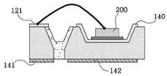
도 1은 종래 기술에 따른 발광 다이오드 패키지의 구조를 개략적으로 도시한단면도로서, 방열판(10) 상부에 인쇄회로기판(11)이 본딩되어 있고, 상기 인쇄회로 기판(11) 상부에 상호 이격된 한 쌍의 실장용 인쇄회로기판(12a,12b)이 본딩되어 있고, 상기 실장용 인쇄회로기판(12a,12b) 상부에 발광 다이오드 패키지(30)가 전기적으로 연결되며 실장되어 있다.1 is a cross-sectional view schematically illustrating a structure of a light emitting diode package according to the related art, in which a printed
그리고, 상기 발광 다이오드 패키지(30)는 상부에 홈이 형성된 히트 슬러그(20)와; 상기 히트 슬러그(20)의 홈 내부에 본딩되며, 상부에 두 단자(22a,22b)를 갖는 서브 마운트 기판(21)과; 상기 서브 마운트 기판(21)의 두 단자(22a,22b)에 플립칩 본딩된 발광 다이오드(25)와; 상기 히브 슬러그(20)를 감싸며, 성형된 플라스틱 사출물(26)과; 상기 플라스틱 사출물(26)에 고정되며, 플라스틱 사출물(26) 측면에 노출된 리드들(27a,27b)과; 상기 서브 마운트 기판(21)의 두 단자(22a,22b)와 리드들(27a,27b)을 전기적으로 연결시키는 와이어(23)와; 상기 발광 다이오드(25)에서 방출되는 광의 분포를 제어하도록 상기 플라스틱 사출물(26)에 고정된 렌즈(22)로 이루어진다.The light
여기서, 상기 발광 다이오드 패키지(30)의 플라스틱 사출물(26)은 상기 실장용 인쇄회로기판(12a,12b)에 본딩되고, 상기 리드들(27a,27b)은 상기 실장용 인쇄회로기판(12a,12b)과 전기적으로 연결되도록 본딩된다.Here, the
이와 같은 종래 기술의 발광 다이오드 패키지는 발광 다이오드 구동 시 발생 하는 열이 열전달 속도가 늦은 인쇄회로기판을 통하여 방열기판(Heat sink)에 전달 됨으로 방열 효과가 미비할 뿐만 아니라 이로 인하여 광 특성이 저하되는 문제점이 있다.Such a conventional LED package has a problem that the heat generated when the LED is driven is transferred to a heat sink through a printed circuit board having a slow heat transfer rate, so that the heat dissipation effect is insignificant and the optical characteristics are deteriorated. There is this.
또한, 서브 마운트 기판, 히트 슬러그와 방열판을 추가로 제작하고, 이를 본 딩하는 공정을 수행함으로써, 부품 수 및 작업공정 증가로 인하여 시간적으로나 경제적으로 제조비용이 증가하게 되는 문제점이 있다.In addition, by further manufacturing the sub-mount substrate, the heat slug and the heat sink, and bonding the same, there is a problem that the manufacturing cost increases in time and economically due to the increase in the number of parts and work process.
본 발명은 상기한 바와 같은 문제점을 해결하기 위하여, 양극 산화(Anodic oxidation) 방법으로 산화시킨 절연성 영역으로 전도성 서브마운트 기판을 양분(兩分)하고, 이 양분된 영역 중 한 영역에 발광 소자를 실장하고, 양분된 다른 한 영역에 발광 소자와 전기적으로 연결한 패키지를 구현함으로써, 패키지 구조를 단순화시키고, 제조 비용을 줄일 수 있는 발광 소자 패키지 및 그의 제조 방법을 제공하는 데 목적이 있다.In order to solve the above problems, the present invention divides the conductive submount substrate into an insulating region oxidized by an anodizing method, and mounts the light emitting device in one of the divided regions. In addition, it is an object of the present invention to provide a light emitting device package and a method of manufacturing the same, by implementing a package electrically connected to the light emitting device in another divided region, thereby simplifying the package structure and reducing the manufacturing cost.
본 발명의 다른 목적은 알루미늄 서브마운트 기판을 통하여 실장된 고출력 발광 소자에 고 전류를 안정적으로 공급하여 고 신뢰성의 패키지를 구현할 수 있는 발광 소자 패키지 및 그의 제조 방법을 제공하는 데 있다.Another object of the present invention is to provide a light emitting device package and a method for manufacturing the same, which can realize a high reliability package by stably supplying a high current to a high output light emitting device mounted through an aluminum submount substrate.
본 발명의 또 다른 목적은 발광 소자에서 방출되는 열 전달 경로를 짧게하여 열 방출효율을 향상시킬 수 있는 발광 소자 패키지 및 그의 제조 방법을 제공하는 데 있다.Still another object of the present invention is to provide a light emitting device package and a method of manufacturing the same, which can shorten the heat transfer path emitted from the light emitting device to improve heat dissipation efficiency.
상기한 본 발명의 목적들을 달성하기 위한 바람직한 제 1 양태(樣態)는,A first preferred aspect for achieving the above objects of the present invention is
절연성 영역에 의해 제 1과 2 영역으로 양분되며, 상기 제 1 영역 상부에 홈이 형성된 전도성 서브마운트 기판과;A conductive submount substrate divided into first and second regions by an insulating region and having a groove formed on the first region;
하부전극과 상부전극을 구비하고, 상기 제 1 영역에 형성된 홈 내부에 실장 되어 상기 하부전극이 상기 제 1 영역과 전기적으로 연결되는 발광 소자와;A light emitting device having a lower electrode and an upper electrode, the light emitting device being mounted in a groove formed in the first region to electrically connect the lower electrode to the first region;
상기 전도성 서브마운트 기판의 제 2 영역 상부에 형성된 전극패드와;An electrode pad formed on the second region of the conductive submount substrate;
상기 전극패드와 상기 발광 소자의 상부전극을 전기적으로 연결하는 도전체를 포함하여 이루어진 발광 소자 패키지가 제공된다.Provided is a light emitting device package including a conductor electrically connecting the electrode pad and an upper electrode of the light emitting device.
상기한 본 발명의 목적들을 달성하기 위한 바람직한 제 2 양태(樣態)는,A second preferred aspect for achieving the above objects of the present invention is
전도성 서브마운트 기판의 상부에 두 상부 영역으로 양분(兩分)하는 제 1 홈을 형성하고, 양분된 한 상부영역 내측에 제 2 홈을 형성하는 단계와;Forming a first groove bisecting two upper regions on the conductive submount substrate, and forming a second groove inside the bisected upper region;
상기 제 1 홈을 제외하고, 상기 전도성 서브마운트 기판 상부에 산화 억제층을 형성하는 단계와;Forming an oxidation inhibiting layer over the conductive submount substrate, except for the first groove;
상기 산화 억제층에 의해 노출된 제 1 홈 내부면의 전도성 서브마운트 기판을 산화시켜 형성된 산화막으로 상기 전도성 서브마운트 기판을 상기 제 2 홈이 있는 제 1 영역과 제 2 영역으로 양분하는 단계와;Dividing the conductive submount substrate into a first region having a second groove and a second region with an oxide film formed by oxidizing a conductive submount substrate on an inner surface of the first groove exposed by the oxidation inhibiting layer;
상기 산화 억제층을 제거하고, 상기 제 2 영역 상부에 전극패드를 형성하는 단계와;Removing the oxidation inhibiting layer and forming an electrode pad on the second region;
상기 제 2 홈에 발광 소자를 본딩하여 상기 발광 소자의 하부에 형성된 금속패드를 상기 제 1 영역에 전기적으로 연결시키고, 상기 발광 소자의 상부에 형성된 금속패드와 상기 제 2 영역의 전극패드를 와이어 본딩하는 단계를 포함하여 이루어진 발광 소자 패키지의 제조 방법이 제공된다.Bonding a light emitting device to the second groove to electrically connect a metal pad formed under the light emitting device to the first area, and wire bonding a metal pad formed on the light emitting device to an electrode pad of the second area. Provided is a method of manufacturing a light emitting device package comprising the steps of:
상기한 본 발명의 목적들을 달성하기 위한 바람직한 제 3 양태(樣態)는,A third preferred aspect for achieving the above objects of the present invention is
전도성 서브마운트 기판의 상부에, 임의의 두 영역과, 이 두 영역을 양분(兩分)하는 제 1 홈과, 양분된 한 영역 내측에 형성된 제 2 홈으로 이루어진 단일 패키지 영역을 복수개 형성하는 단계와;Forming a plurality of single package regions on the conductive submount substrate, the plurality of single package regions consisting of any two regions, a first groove bisecting the two regions, and a second groove formed inside the bisected region; ;
상기 각각의 단일 패키지 영역의 제 1 홈을 제외하고, 상기 전도성 서브마운트 기판 상부에 산화 억제층을 형성하는 단계와;Forming an oxidation inhibiting layer over the conductive submount substrate, except for the first groove of each single package region;
상기 산화 억제층에 의해 노출된 제 1 홈 내부면의 전도성 서브마운트 기판을 산화시켜 형성된 산화막으로 각각의 단일 패키지 영역을 상기 제 2 홈이 있는 제 1 영역과 제 2 영역으로 양분하는 단계와;Dividing each single package region into a first region having a second groove and a second region with an oxide film formed by oxidizing a conductive submount substrate on the inner surface of the first groove exposed by the oxidation inhibiting layer;
상기 산화 억제층을 제거하고, 상기 각각의 단일 패키지 영역의 제 2 영역 상부에 전극패드를 형성하고, 상기 제 2 홈 내부면에 전도성 반사막을 형성하는 단계와;Removing the redox layer, forming an electrode pad over the second region of each single package region, and forming a conductive reflective film on the inner surface of the second groove;
상기 각각의 단일 패키지 영역에 있는 제 1 영역과 제 2 영역 하부 각각에 솔더를 형성하는 단계와;Forming solder in each of the first region and the lower portion of the second region in each single package region;
상기 각각의 단일 패키지 영역에 있는 제 2 홈에 발광 소자를 본딩하고, 상기 발광 소자의 상부에 형성된 금속패드와 상기 제 2 영역의 전극패드를 와이어 본딩하는 단계와;Bonding a light emitting element to a second groove in each single package region, and wire bonding a metal pad formed on the light emitting element and an electrode pad of the second region;
상기 각각의 단일 패키지 영역을 분리시키는 단계를 포함하여 이루어진 발광 소자 패키지의 제조 방법이 제공된다.Provided is a method of manufacturing a light emitting device package comprising separating each single package region.
이하, 첨부된 도면을 참조하여 본 발명의 바람직한 실시예를 설명하면 다음과 같다.Hereinafter, exemplary embodiments of the present invention will be described with reference to the accompanying drawings.
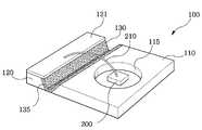
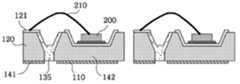
도 2는 본 발명에 따른 발광 소자 패키지의 개략적인 사시도로서, 본 발명의 발광 소자 패키지는 절연성 영역에 의해 제 1과 2 영역(110,120)으로 양분되며, 상기 제 1 영역(110) 상부에 홈(115)이 형성된 전도성 서브마운트 기판(100)과; 하부전극과 상부전극을 구비하고, 상기 제 1 영역(110)에 형성된 홈(115) 내부에 실장되어 상기 하부전극이 상기 제 1 영역과 전기적으로 연결되는 발광 소자(200)와; 상기 전도성 서브마운트 기판(100)의 제 2 영역(120) 상부에 형성된 전극패드(121)와; 상기 전극패드(121)와 상기 발광 소자(200)의 상부전극을 전기적으로 연결하는 와이어(210)로 구성된다.FIG. 2 is a schematic perspective view of a light emitting device package according to the present invention, wherein the light emitting device package of the present invention is divided into first and
여기서, 상기 절연성 영역은 상기 제 1과 2 영역(110) 각각이 전기적으로 독립되도록, 상기 제 1과 2 영역(110) 사이의 상기 전도성 서브마운트 기판(100) 영역을 산화시켜 형성된 산화막(135)으로 이루어진 것이 바람직하다.The
이 때, 상기 산화막(135)은, 상기 제 1과 2 영역(110) 사이의 상기 전도성 서브마운트 기판(100) 영역에 홈(130)을 형성하고, 이 홈(130)의 양측면과 바닥면을 산화시켜 만들어진 것이 더 바람직하다.In this case, the
그리고, 상기 제 1 영역(110)에 형성된 홈(115)을 원형 그루브(Groove) 형상으로 형성하면, 상기 발광 소자(200)의 측면에서 방출된 광을 상부로 반사시켜 발광 효율을 증대할 수 있는 것이다.In addition, when the
그러므로, 본 발명의 발광 소자 패키지는 간단한 구조의 전도성 서브마운트 기판(100)에 발광 소자를 실장함으로써, 패키지를 구성하는 부품수를 줄일 수 있어 저가로 제조할 수 있는 장점이 있다.Therefore, the light emitting device package of the present invention has an advantage that the number of parts constituting the package can be reduced and manufactured at low cost by mounting the light emitting device on the
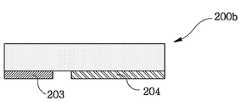
도 3a와 3b는 본 발명에 따른 발광 소자 패키지에 실장되는 발광 소자를 설명하기 위한 단면도로서, 도 3a의 발광 소자(200a)는 소자의 상부 및 하부에 금속패드 '201'과 '202'가 형성되어 있는 구조이고, 도 3b의 발광 소자(200b)는 소자의 하부에 금속패드 '203'과 '204'가 형성되어 있는 구조이다.3A and 3B are cross-sectional views illustrating a light emitting device mounted on a light emitting device package according to the present invention. In the
본 발명의 발광 소자 패키지는 도 3a의 발광 소자가 실장된다.In the light emitting device package of the present invention, the light emitting device of FIG. 3A is mounted.
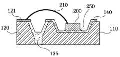
도 4a 내지 4d는 본 발명에 따른 발광 소자 패키지의 여러 실시예를 설명하기 위한 단면도로서, 먼저, 도 4a의 발광 소자 패키지는 산화막(135)에 의해 제 1과 2 영역(110,120)으로 양분된 전도성 서브마운트 기판(100)의 제 1 영역(110) 상부에 형성된 홈(115)에 발광 소자(200)가 플립칩(Flip chip) 본딩되어 있다.4A to 4D are cross-sectional views illustrating various embodiments of a light emitting device package according to the present invention. First, the light emitting device package of FIG. 4A is divided into first and
그리고, 상기 발광 소자(200) 상부에 형성된 금속패드와 상기 제 2 영역(120) 상부에 형성된 전극패드(121)가 와이어(210)로 본딩되어 있다.In addition, the metal pad formed on the
즉, 상기 발광 소자(200) 상부에 형성된 금속패드는 와이어 본딩된 전극패드(121)를 통하여 전도성 서브마운트 기판(100)의 제 2 영역(120)과 전기적으로 연결되고, 상기 발광 소자(200)의 하부에 형성된 금속패드는 전도성 페이스트(250)와 같은 접착제에 의해 본딩과 동시에 전도성 서브마운트 기판(100)의 제 1 영역(110)과 전기적으로 연결된다.That is, the metal pad formed on the
그리고, 도 4b의 발광 소자 패키지는 전도성 서브마운트 기판(100)의 제 1 영역(110)과 제 2 영역(120) 각각의 하부에 솔더(141,142)가 형성되어 있다.In the light emitting device package of FIG. 4B, solders 141 and 142 are formed under each of the
이렇게 형성된 솔더(141,142)는 발광 소자 패키지가 보다 쉽게 마더 보드(Mother board)에 실장될 수 있게 도와준다.The
또한, 도 4c의 발광 소자 패키지는 전도성 서브마운트 기판(100)의 제 1 영역(110) 상부에 형성된 홈(115) 내부면에 전도성 반사막(140)이 형성되어 있고, 이 전도성 반사막(140) 상부에 발광 소자(200)가 본딩되어 있다.In addition, in the light emitting device package of FIG. 4C, a conductive
즉, 상기 발광 소자(200)에서 방출된 광은 상기 전도성 반사막(140)에서 반사되어 상부로 진행하게 되어, 발광 소자 패키지의 광출력을 증대시킬 수 있는 것이다.That is, the light emitted from the
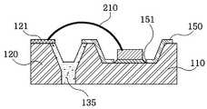
더불어, 도 4d의 발광 소자 패키지는 전도성 서브마운트 기판(100)의 제 1 영역(110) 상부에 형성된 홈(115) 내부면에 비전도성 반사막(150)이 형성되어 있고, 상기 비전도성 반사막(150)에는 홈(115) 바닥면의 일부가 도출되는 개구(151)가 형성되어 있고, 상기 비전도성 반사막(150)의 개구(151)에 의해 노출된 홈(115) 바닥면에 발광 소자(200)가 본딩되어 있다.In addition, in the light emitting device package of FIG. 4D, a nonconductive
그러므로, 상기 발광 소자(200)의 하부에 형성된 금속패드는 상기 전도성 서브마운트 기판(100)의 제 1 영역(110)에 전기적으로 연결되는 것이다.Therefore, the metal pad formed under the
전술된 발광 소자 패키지들의 전도성 서브마운트 기판은 두께가 100 ~ 1000㎛가 바람직하고, 그 기판의 재질은 알루미늄으로 사용하는 것이 바람직하다.The conductive submount substrate of the above-described light emitting device packages preferably has a thickness of 100 to 1000 μm, and the material of the substrate is preferably aluminum.
즉, 상기 전도성 서브마운트 기판은 알루미늄 시트(Sheet)를 사용하는 것이다.That is, the conductive submount substrate uses an aluminum sheet.
그리고, 상기 전도성 반사막(140)과 비전도성 반사막(150)은 상기 전도성 서브마운트 기판(100)과 접착력이 우수한 접착층과 발광 소자의 광을 효율적으로 반사시킬 수 있도록 반사 효율이 우수한 미러(Mirror)층으로 형성될 수 있다.In addition, the conductive
이 때, 접착층과 미러층 사이에는 배리어층(Barrier layer)을 형성하여, 후 공정에서 100 ~ 400도의 고온에 노출되는 경우 접착층의 물질이 미러층으로 확산되어 반사 효율이 저하되는 것을 방지하는 것이 바람직하다.In this case, it is preferable to form a barrier layer between the adhesive layer and the mirror layer so as to prevent the material of the adhesive layer from diffusing into the mirror layer and decreasing the reflection efficiency when exposed to a high temperature of 100 to 400 degrees in a later step. Do.
그러므로, 상기 전도성 서브마운트 기판이 알루미늄 시트인 경우, 상기 전도성 반사막(140)은 접착층으로 Ti층, 배리어층으로 Pt층과 미러층으로 Ag층으로 형성하는데, 스퍼터링 방법 또는 이빔 이베퍼레이션(E-beam evaporation) 방법으로 순차적으로 증착하여 형성한다.Therefore, when the conductive submount substrate is an aluminum sheet, the conductive
한편, 상기 발광 소자(200)가 실장된 홈(115) 내부에는 상기 발광 소자(200)를 감싸며 형광체, 실리콘 젤과 투광성이 우수한 에폭시 중 어느 하나가 충진되어 있는 것이 바람직하다.On the other hand, the
그리고, 상기 발광 소자(200)에서 방출된 광의 분포를 제어하기 위하여 렌즈를 상기 전도성 서브마운트 기판에 본딩하는 것이 바람직하다.In addition, in order to control the distribution of light emitted from the
전술된 바와 같이, 본 발명에 따른 발광 소자 패키지는 전도성 서브마운트 기판을 알루미늄으로 사용한 경우, 고출력 발광 소자를 패키징한 때에도 상기 알루미늄 서브마운트 기판을 통하여 고 전류를 안정적으로 발광 소자에 공급할 수 있어, 고 신뢰성의 패키지를 구현할 수 있는 장점이 있다.As described above, the light emitting device package according to the present invention can stably supply high current to the light emitting device through the aluminum submount substrate even when the high power light emitting device is packaged when the conductive submount substrate is used as aluminum. It has the advantage of implementing a package of reliability.
그리고, 구조가 단순하여 발광 소자에서 방출되는 열 전달 경로를 짧게하여 열 방출효율을 향상시킬 수 있는 장점이 있다.In addition, since the structure is simple, there is an advantage of improving heat dissipation efficiency by shortening the heat transfer path emitted from the light emitting device.
도 5는 본 발명에 따른 발광 소자 패키지에 실장된 발광소자에서 방출되는 광의 경로를 설명하기 위한 개념도로서, 발광 소자 패키지의 전도성 서브마운트 기판에 형성된 홈(115) 내부의 측면은 'θ'의 각도로 경사져 있는 것이 바람직하다.FIG. 5 is a conceptual view illustrating a path of light emitted from a light emitting device mounted on a light emitting device package according to the present invention. The side surface of the
즉, 상기 홈(115) 내부의 측면이 경사져 있으면, 발광 소자에서 방출된 광이 홈(115) 내부의 측면에서 반사되어 발광 소자 상부로 진행하게 되어 광출력을 향상시킬 수 있게 된다.That is, if the side surface of the
도 6a 내지 6f는 본 발명에 따른 발광 소자 패키지를 제조하는 공정을 설명하기 위한 단면도로서, 전도성 서브마운트 기판(100)의 상부에 두 상부 영역으로 양분(兩分)하는 제 1 홈(130a)을 형성하고, 양분된 한 상부영역 내측에 제 2 홈(115a)을 형성한다.(도 6a)6A through 6F are cross-sectional views illustrating a process of manufacturing a light emitting device package according to the present invention, and include a
그 후, 상기 제 1 홈(130a)을 제외하고, 상기 전도성 서브마운트 기판(100) 상부에 산화 억제층(500)을 형성한다.(도 6b)Thereafter, except for the
여기서, 상기 산화 억제층(500)은 후술되는 산화 공정에서 상기 산화 억제층(500)에 의해 노출된 제 1 홈(130a) 내부면의 전도성 서브마운트 기판(100) 영역만 산화되고, 나머지 전도성 서브마운트 기판(100) 영역은 산화되지 못하게 하는 기능을 수행한다.Here, the
연이어, 상기 산화 억제층(500)에 의해 노출된 제 1 홈(130a) 내부면의 전도성 서브마운트 기판(100)을 산화시켜 형성된 산화막(135)으로 상기 전도성 서브마운트 기판(100)을 상기 제 2 홈(115a)이 있는 제 1 영역(110)과 제 2 영역(120)으 로 양분한다.(도 6c)Subsequently, the
여기서, 상기 산화 공정은 질소산(Nitric acid) 또는 붕소산(Boric acid)와 같은 전해액(Electrolytes)을 이용한 양극 산화(Anodic oxidation) 방법을 수행하는 것이 바람직하다.Here, the oxidation process is preferably performed by the anodic oxidation (Anodic oxidation) method using an electrolyte (Electrolytes), such as nitric acid (Nitric acid) or boric acid (Boric acid).
이 때, 상기 전해액의 온도는 10 ~ 50도가 적당하고, 펄스 전류(Pulsed current)를 인가한다.At this time, the temperature of the electrolyte is 10 ~ 50 degrees is appropriate, and a pulsed current (Pulsed current) is applied.
그리고, 상기 전해액에 산화막의 두께 및 강도를 증가시키기 위하여 유황산(Sulfuric acid)를 첨가하는 것이 바람직하다.In addition, it is preferable to add sulfuric acid (Sulfuric acid) to increase the thickness and strength of the oxide film to the electrolyte.
또한, 상기 산화 억제층(500)은 양극 산화 공정시 사용되는 전해액(Electrolytes)에 반응이 없어야 하며, 산화막 형성 후, 산화 억제층(500)이 제거될 때, 전도성 서브마운트 기판(100) 및 산화막(135)의 손상없이 제거될 수 있는 물질이어야 한다.In addition, the
즉, 상기 산화 억제층(500)은 폴리머(Polymer) 계열의 물질 또는 금속 물질로 형성할 수 있다.That is, the
그 다음, 상기 산화 억제층(500)을 제거한다.(도 6d)Then, the
이어서, 상기 제 2 영역(120) 상부에 전극패드(121)를 형성한다.(도 6e)Subsequently, an
마지막으로, 상기 제 2 홈(115a)에 발광 소자(200)를 본딩하여 상기 발광 소자(200)의 하부에 형성된 금속패드를 상기 제 1 영역(110)에 전기적으로 연결시키고, 상기 발광 소자(200)의 상부에 형성된 금속패드와 상기 제 2 영역(120)의 전극패드(121)를 와이어 본딩한다.(도 6f)Finally, the
도 7은 본 발명에 따른 발광 소자 패키지의 홈에 반사막을 형성하는 공정을 설명하기 위한 단면도로서, 전술된 도 6e와 도 6f의 공정 사이에, 전도성 서브마운트 기판(100)의 제 2 홈(115a) 내부면에 전도성 반사막(140)을 형성하는 공정을 더 수행하는 것이 바람직하다.FIG. 7 is a cross-sectional view illustrating a process of forming a reflective film in a groove of a light emitting device package according to the present invention. Between the processes of FIGS. 6E and 6F, the
즉, 상기 전도성 반사막(140) 상부에는 발광 소자(200)가 본딩되고, 이 발광 소자(200)의 측면에서 방출되는 광은 상기 전도성 반사막(140)에서 반사되어 발광 소자(200) 상부로 출사되는 것이다.That is, the
도 8a와 8b는 본 발명에 따른 발광 소자 패키지의 하부에 솔더를 형성하는 공정을 설명하기 위한 단면도로서, 먼저, 도 8a는 전술된 도 7의 공정을 수행한 후에, 전도성 서브마운트 기판(100)의 제 1 영역(110)과 제 2 영역(110,120) 하부 각각에 솔더(141,142)를 형성하는 공정을 수행하는 것이다.8A and 8B are cross-sectional views illustrating a process of forming solder in a lower portion of a light emitting device package according to the present invention. First, FIG. 8A illustrates a
그리고, 도 8b는 도 8a의 공정을 수행한 후에, 전도성 반사막(140) 상부에 발광 소자(200)를 본딩하고, 상기 발광 소자(200)의 상부에 형성된 금속패드와 상기 제 2 영역(120)의 전극패드(121)를 와이어 본딩하는 것이다.In addition, after performing the process of FIG. 8A, FIG. 8B bonds the
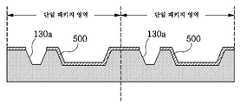
도 9a 내지 9g는 본 발명에 따른 복수개의 발광 소자 패키지들을 서브마운트 기판에 제조하는 공정을 설명하기 위한 개략적인 단면도로서, 전도성 서브마운트 기판(100)의 상부에, 임의의 두 영역(A영역,B영역)과, 이 두 영역(A영역,B영역)을 양분(兩分)하는 제 1 홈(130a)과, 양분된 한 영역(B영역) 내측에 형성된 제 2 홈(115a)으로 이루어진 단일 패키지 영역을 복수개 형성한다.(도 9a)9A to 9G are schematic cross-sectional views illustrating a process of manufacturing a plurality of light emitting device packages according to an exemplary embodiment of the present invention on a submount substrate. Area B), a
그 다음, 상기 각각의 단일 패키지 영역의 제 1 홈(130a)을 제외하고, 상기 전도성 서브마운트 기판(100) 상부에 산화 억제층(500)을 형성한다.(도 9b)Then, an
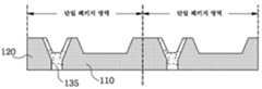
이어서, 상기 산화 억제층(500)에 의해 노출된 제 1 홈(130a) 내부면의 전도성 서브마운트 기판(100)을 산화시켜 형성된 산화막(135)으로 각각의 단일 패키지 영역을 상기 제 2 홈(115a)이 있는 제 1 영역(110)과 제 2 영역(120)으로 양분한다.(도 9c)Subsequently, each single package region is formed of an
연이어, 상기 산화 억제층(500)을 제거한다.(도 9d)Subsequently, the
계속하여, 상기 각각의 단일 패키지 영역의 제 2 영역(120) 상부에 전극패드(121)를 형성하고, 상기 제 2 홈(115a) 내부면에 전도성 반사막(140)을 형성한다.(도 9e)Subsequently, an
그 다음, 상기 각각의 단일 패키지 영역에 있는 제 1 영역(110)과 제 2 영역(110,120) 하부 각각에 솔더(141,142)를 형성한다.(도 9f)Next, solders 141 and 142 are formed in the lower portions of the
이어서, 상기 각각의 단일 패키지 영역에 있는 제 2 홈(115a)에 발광 소자(200)를 본딩하고, 상기 발광 소자(200)의 상부에 형성된 금속패드와 상기 제 2 영역(120)의 전극패드(121)를 와이어 본딩한다.(도 9g)Subsequently, the
마지막으로, 상기 각각의 단일 패키지 영역이 분리시킨다.(도 9h)Finally, each single package region separates (FIG. 9H).
따라서, 도 9h의 공정으로 본 발명에 따른 패키지가 완성된다.Thus, the package according to the present invention is completed by the process of FIG. 9H.
이상 상술한 바와 같이, 본 발명은 양극 산화(Anodic oxidation) 방법으로 산화시킨 절연성 영역으로 전도성 서브마운트 기판을 양분(兩分)하고, 이 양분된 영역 중 한 영역에 발광 소자를 실장하고, 양분된 다른 한 영역에 발광 소자와 전기적으로 연결한 패키지를 구현함으로써, 패키지 구조를 단순화시키고, 제조 비용을 줄일 수 있는 효과가 있다.As described above, the present invention divides the conductive submount substrate into an insulating region oxidized by an anodizing method, mounts a light emitting device in one of the divided regions, and By implementing a package electrically connected to the light emitting device in another area, the package structure can be simplified and manufacturing costs can be reduced.
또한, 본 발명은 알루미늄 서브마운트 기판을 통하여 실장된 고출력 발광 소자에 고 전류를 안정적으로 공급하여 고 신뢰성의 패키지를 구현할 수 있는 효과가 있다.In addition, the present invention has the effect of stably supplying a high current to the high output light emitting device mounted through the aluminum submount substrate to implement a package of high reliability.
게다가, 본 발명은 발광 소자에서 방출되는 열 전달 경로를 짧게하여 열 방출효율을 향상시킬 수 있는 효과가 있다.In addition, the present invention has the effect of improving the heat dissipation efficiency by shortening the heat transfer path emitted from the light emitting device.
본 발명은 구체적인 예에 대해서만 상세히 설명되었지만 본 발명의 기술사상 범위 내에서 다양한 변형 및 수정이 가능함은 당업자에게 있어서 명백한 것이며, 이러한 변형 및 수정이 첨부된 특허청구범위에 속함은 당연한 것이다.Although the invention has been described in detail only with respect to specific examples, it will be apparent to those skilled in the art that various modifications and variations are possible within the spirit of the invention, and such modifications and variations belong to the appended claims.
Claims (20)
Translated fromKoreanPriority Applications (1)
| Application Number | Priority Date | Filing Date | Title |
|---|---|---|---|
| KR1020050093767AKR100699161B1 (en) | 2005-10-06 | 2005-10-06 | Light emitting device package and manufacturing method thereof |
Applications Claiming Priority (1)
| Application Number | Priority Date | Filing Date | Title |
|---|---|---|---|
| KR1020050093767AKR100699161B1 (en) | 2005-10-06 | 2005-10-06 | Light emitting device package and manufacturing method thereof |
Publications (1)
| Publication Number | Publication Date |
|---|---|
| KR100699161B1true KR100699161B1 (en) | 2007-03-22 |
Family
ID=41564374
Family Applications (1)
| Application Number | Title | Priority Date | Filing Date |
|---|---|---|---|
| KR1020050093767AExpired - Fee RelatedKR100699161B1 (en) | 2005-10-06 | 2005-10-06 | Light emitting device package and manufacturing method thereof |
Country Status (1)
| Country | Link |
|---|---|
| KR (1) | KR100699161B1 (en) |
Cited By (7)
| Publication number | Priority date | Publication date | Assignee | Title |
|---|---|---|---|---|
| KR100998010B1 (en) | 2008-04-28 | 2010-12-03 | 삼성엘이디 주식회사 | Light emitting device package and its manufacturing method |
| KR101122059B1 (en) | 2008-07-16 | 2012-03-14 | 주식회사 이츠웰 | A Surface Mount Device Type Light Emmitting Diode and Backlight Unit Uusing The Same |
| WO2013074630A1 (en)* | 2011-11-15 | 2013-05-23 | Cree, Inc. | Light emitting diode (led) packages and related methods |
| CN103325919A (en)* | 2013-06-27 | 2013-09-25 | 深圳市东昊光电子有限公司 | LED manufacturing technology of L-shaped metal base plate and base plate |
| KR101552422B1 (en)* | 2014-01-14 | 2015-09-10 | 성균관대학교산학협력단 | Substrate for light emitting diode and method of manufacturing the same and light source apparatus including the substrate |
| KR101681343B1 (en) | 2008-12-30 | 2016-11-30 | 오스람 옵토 세미컨덕터스 게엠베하 | Method for producing lamps |
| US10741737B2 (en) | 2017-12-14 | 2020-08-11 | Samsung Electronics Co., Ltd. | Light emitting device package |
Citations (4)
| Publication number | Priority date | Publication date | Assignee | Title |
|---|---|---|---|---|
| JP2003037293A (en) | 2001-07-25 | 2003-02-07 | Nichia Chem Ind Ltd | Chip component type light emitting device and method of manufacturing the same |
| JP2003324216A (en) | 2002-02-28 | 2003-11-14 | Rohm Co Ltd | Light emitting diode lamp |
| JP2004022588A (en) | 2002-06-12 | 2004-01-22 | New Japan Radio Co Ltd | Optical semiconductor device |
| JP2004119981A (en) | 2002-09-27 | 2004-04-15 | Kokuren Koden Kagi Kofun Yugenkoshi | High power light emitting diode planar mounting structure and method of manufacturing the same |
- 2005
- 2005-10-06KRKR1020050093767Apatent/KR100699161B1/ennot_activeExpired - Fee Related
Patent Citations (4)
| Publication number | Priority date | Publication date | Assignee | Title |
|---|---|---|---|---|
| JP2003037293A (en) | 2001-07-25 | 2003-02-07 | Nichia Chem Ind Ltd | Chip component type light emitting device and method of manufacturing the same |
| JP2003324216A (en) | 2002-02-28 | 2003-11-14 | Rohm Co Ltd | Light emitting diode lamp |
| JP2004022588A (en) | 2002-06-12 | 2004-01-22 | New Japan Radio Co Ltd | Optical semiconductor device |
| JP2004119981A (en) | 2002-09-27 | 2004-04-15 | Kokuren Koden Kagi Kofun Yugenkoshi | High power light emitting diode planar mounting structure and method of manufacturing the same |
Cited By (8)
| Publication number | Priority date | Publication date | Assignee | Title |
|---|---|---|---|---|
| KR100998010B1 (en) | 2008-04-28 | 2010-12-03 | 삼성엘이디 주식회사 | Light emitting device package and its manufacturing method |
| KR101122059B1 (en) | 2008-07-16 | 2012-03-14 | 주식회사 이츠웰 | A Surface Mount Device Type Light Emmitting Diode and Backlight Unit Uusing The Same |
| KR101681343B1 (en) | 2008-12-30 | 2016-11-30 | 오스람 옵토 세미컨덕터스 게엠베하 | Method for producing lamps |
| WO2013074630A1 (en)* | 2011-11-15 | 2013-05-23 | Cree, Inc. | Light emitting diode (led) packages and related methods |
| US10043960B2 (en) | 2011-11-15 | 2018-08-07 | Cree, Inc. | Light emitting diode (LED) packages and related methods |
| CN103325919A (en)* | 2013-06-27 | 2013-09-25 | 深圳市东昊光电子有限公司 | LED manufacturing technology of L-shaped metal base plate and base plate |
| KR101552422B1 (en)* | 2014-01-14 | 2015-09-10 | 성균관대학교산학협력단 | Substrate for light emitting diode and method of manufacturing the same and light source apparatus including the substrate |
| US10741737B2 (en) | 2017-12-14 | 2020-08-11 | Samsung Electronics Co., Ltd. | Light emitting device package |
Similar Documents
| Publication | Publication Date | Title |
|---|---|---|
| US8035121B2 (en) | Package for light emitting device having a lens spaced from a light emitting device module | |
| CN107482106B (en) | Light source circuit unit, illuminator and display | |
| EP2385549B1 (en) | Chip package, package module, and illumination apparatus including chip package module | |
| AU2006254610B2 (en) | Package structure of semiconductor light-emitting device | |
| CN100442546C (en) | Light-emitting element, manufacturing method thereof, and lead frame for manufacturing light-emitting element | |
| KR100851183B1 (en) | Semiconductor light emitting device package | |
| US8017964B2 (en) | Light emitting device | |
| KR101622399B1 (en) | Led device | |
| KR20050012372A (en) | Luminescent diode package and method for manufacturing led package | |
| US20100084673A1 (en) | Light-emitting semiconductor packaging structure without wire bonding | |
| JP2014082481A (en) | Light emitting device | |
| KR100699161B1 (en) | Light emitting device package and manufacturing method thereof | |
| KR100667504B1 (en) | Package of light emitting device and manufacturing method thereof | |
| EP2813758A2 (en) | Light emitting module | |
| KR100645657B1 (en) | White light emitting diode module with flip chip printed circuit board and flip chip printed circuit board | |
| CN101504938A (en) | Light emitting diode packaging structure and light emitting diode packaging method | |
| KR100839122B1 (en) | A side emitting type LED lamp, a manufacturing method thereof, and a light emitting device including the LED lamp | |
| JP2002232015A (en) | Semiconductor light emitting device | |
| KR100650263B1 (en) | Light emitting device package and manufacturing method thereof | |
| KR20100046558A (en) | Light emitting diode package and method for manufacturing the same | |
| CN223080441U (en) | Fusion packaging structure of driving IC and LED chip and light-emitting device | |
| KR102532362B1 (en) | Light emitting device package | |
| US8882312B2 (en) | Light emitting device with light emitting diodes fixed to printed circuit | |
| KR101146659B1 (en) | Optical package and manufacturing method of the same | |
| KR102558584B1 (en) | Light emitting device package |
Legal Events
| Date | Code | Title | Description |
|---|---|---|---|
| A201 | Request for examination | ||
| PA0109 | Patent application | St.27 status event code:A-0-1-A10-A12-nap-PA0109 | |
| PA0201 | Request for examination | St.27 status event code:A-1-2-D10-D11-exm-PA0201 | |
| R17-X000 | Change to representative recorded | St.27 status event code:A-3-3-R10-R17-oth-X000 | |
| D13-X000 | Search requested | St.27 status event code:A-1-2-D10-D13-srh-X000 | |
| D14-X000 | Search report completed | St.27 status event code:A-1-2-D10-D14-srh-X000 | |
| E902 | Notification of reason for refusal | ||
| PE0902 | Notice of grounds for rejection | St.27 status event code:A-1-2-D10-D21-exm-PE0902 | |
| P11-X000 | Amendment of application requested | St.27 status event code:A-2-2-P10-P11-nap-X000 | |
| P13-X000 | Application amended | St.27 status event code:A-2-2-P10-P13-nap-X000 | |
| E701 | Decision to grant or registration of patent right | ||
| PE0701 | Decision of registration | St.27 status event code:A-1-2-D10-D22-exm-PE0701 | |
| PR1002 | Payment of registration fee | St.27 status event code:A-2-2-U10-U11-oth-PR1002 Fee payment year number:1 | |
| GRNT | Written decision to grant | ||
| PR0701 | Registration of establishment | St.27 status event code:A-2-4-F10-F11-exm-PR0701 | |
| PG1601 | Publication of registration | St.27 status event code:A-4-4-Q10-Q13-nap-PG1601 | |
| PN2301 | Change of applicant | St.27 status event code:A-5-5-R10-R13-asn-PN2301 St.27 status event code:A-5-5-R10-R11-asn-PN2301 | |
| P22-X000 | Classification modified | St.27 status event code:A-4-4-P10-P22-nap-X000 | |
| R18-X000 | Changes to party contact information recorded | St.27 status event code:A-5-5-R10-R18-oth-X000 | |
| R18-X000 | Changes to party contact information recorded | St.27 status event code:A-5-5-R10-R18-oth-X000 | |
| PR1001 | Payment of annual fee | St.27 status event code:A-4-4-U10-U11-oth-PR1001 Fee payment year number:4 | |
| PR1001 | Payment of annual fee | St.27 status event code:A-4-4-U10-U11-oth-PR1001 Fee payment year number:5 | |
| PR1001 | Payment of annual fee | St.27 status event code:A-4-4-U10-U11-oth-PR1001 Fee payment year number:6 | |
| FPAY | Annual fee payment | Payment date:20130226 Year of fee payment:7 | |
| PR1001 | Payment of annual fee | St.27 status event code:A-4-4-U10-U11-oth-PR1001 Fee payment year number:7 | |
| FPAY | Annual fee payment | Payment date:20140224 Year of fee payment:8 | |
| PR1001 | Payment of annual fee | St.27 status event code:A-4-4-U10-U11-oth-PR1001 Fee payment year number:8 | |
| FPAY | Annual fee payment | Payment date:20150224 Year of fee payment:9 | |
| PR1001 | Payment of annual fee | St.27 status event code:A-4-4-U10-U11-oth-PR1001 Fee payment year number:9 | |
| PN2301 | Change of applicant | St.27 status event code:A-5-5-R10-R13-asn-PN2301 St.27 status event code:A-5-5-R10-R11-asn-PN2301 | |
| FPAY | Annual fee payment | Payment date:20160224 Year of fee payment:10 | |
| PR1001 | Payment of annual fee | St.27 status event code:A-4-4-U10-U11-oth-PR1001 Fee payment year number:10 | |
| FPAY | Annual fee payment | Payment date:20170224 Year of fee payment:11 | |
| PR1001 | Payment of annual fee | St.27 status event code:A-4-4-U10-U11-oth-PR1001 Fee payment year number:11 | |
| FPAY | Annual fee payment | Payment date:20180223 Year of fee payment:12 | |
| PR1001 | Payment of annual fee | St.27 status event code:A-4-4-U10-U11-oth-PR1001 Fee payment year number:12 | |
| PR1001 | Payment of annual fee | St.27 status event code:A-4-4-U10-U11-oth-PR1001 Fee payment year number:13 | |
| PC1903 | Unpaid annual fee | St.27 status event code:A-4-4-U10-U13-oth-PC1903 Not in force date:20200317 Payment event data comment text:Termination Category : DEFAULT_OF_REGISTRATION_FEE | |
| PN2301 | Change of applicant | St.27 status event code:A-5-5-R10-R13-asn-PN2301 St.27 status event code:A-5-5-R10-R11-asn-PN2301 | |
| PC1903 | Unpaid annual fee | St.27 status event code:N-4-6-H10-H13-oth-PC1903 Ip right cessation event data comment text:Termination Category : DEFAULT_OF_REGISTRATION_FEE Not in force date:20200317 | |
| P22-X000 | Classification modified | St.27 status event code:A-4-4-P10-P22-nap-X000 |