KR100698742B1 - Semiconductor device manufacturing method - Google Patents
Semiconductor device manufacturing methodDownload PDFInfo
- Publication number
- KR100698742B1 KR100698742B1KR1020050100142AKR20050100142AKR100698742B1KR 100698742 B1KR100698742 B1KR 100698742B1KR 1020050100142 AKR1020050100142 AKR 1020050100142AKR 20050100142 AKR20050100142 AKR 20050100142AKR 100698742 B1KR100698742 B1KR 100698742B1
- Authority
- KR
- South Korea
- Prior art keywords
- tungsten
- barrier metal
- metal layer
- gas
- forming
- Prior art date
- Legal status (The legal status is an assumption and is not a legal conclusion. Google has not performed a legal analysis and makes no representation as to the accuracy of the status listed.)
- Expired - Fee Related
Links
Images


Classifications
- H—ELECTRICITY
- H01—ELECTRIC ELEMENTS
- H01L—SEMICONDUCTOR DEVICES NOT COVERED BY CLASS H10
- H01L21/00—Processes or apparatus adapted for the manufacture or treatment of semiconductor or solid state devices or of parts thereof
- H01L21/70—Manufacture or treatment of devices consisting of a plurality of solid state components formed in or on a common substrate or of parts thereof; Manufacture of integrated circuit devices or of parts thereof
- H01L21/71—Manufacture of specific parts of devices defined in group H01L21/70
- H01L21/768—Applying interconnections to be used for carrying current between separate components within a device comprising conductors and dielectrics
- H01L21/76838—Applying interconnections to be used for carrying current between separate components within a device comprising conductors and dielectrics characterised by the formation and the after-treatment of the conductors
- H01L21/76877—Filling of holes, grooves or trenches, e.g. vias, with conductive material
- H01L21/76883—Post-treatment or after-treatment of the conductive material
- H—ELECTRICITY
- H01—ELECTRIC ELEMENTS
- H01L—SEMICONDUCTOR DEVICES NOT COVERED BY CLASS H10
- H01L21/00—Processes or apparatus adapted for the manufacture or treatment of semiconductor or solid state devices or of parts thereof
- H01L21/02—Manufacture or treatment of semiconductor devices or of parts thereof
- H01L21/02041—Cleaning
- H01L21/02057—Cleaning during device manufacture
- H01L21/02068—Cleaning during device manufacture during, before or after processing of conductive layers, e.g. polysilicon or amorphous silicon layers
- H—ELECTRICITY
- H01—ELECTRIC ELEMENTS
- H01L—SEMICONDUCTOR DEVICES NOT COVERED BY CLASS H10
- H01L21/00—Processes or apparatus adapted for the manufacture or treatment of semiconductor or solid state devices or of parts thereof
- H01L21/02—Manufacture or treatment of semiconductor devices or of parts thereof
- H01L21/04—Manufacture or treatment of semiconductor devices or of parts thereof the devices having potential barriers, e.g. a PN junction, depletion layer or carrier concentration layer
- H01L21/18—Manufacture or treatment of semiconductor devices or of parts thereof the devices having potential barriers, e.g. a PN junction, depletion layer or carrier concentration layer the devices having semiconductor bodies comprising elements of Group IV of the Periodic Table or AIIIBV compounds with or without impurities, e.g. doping materials
- H01L21/30—Treatment of semiconductor bodies using processes or apparatus not provided for in groups H01L21/20 - H01L21/26
- H01L21/31—Treatment of semiconductor bodies using processes or apparatus not provided for in groups H01L21/20 - H01L21/26 to form insulating layers thereon, e.g. for masking or by using photolithographic techniques; After treatment of these layers; Selection of materials for these layers
- H01L21/3205—Deposition of non-insulating-, e.g. conductive- or resistive-, layers on insulating layers; After-treatment of these layers
- H01L21/321—After treatment
- H01L21/3213—Physical or chemical etching of the layers, e.g. to produce a patterned layer from a pre-deposited extensive layer
- H01L21/32133—Physical or chemical etching of the layers, e.g. to produce a patterned layer from a pre-deposited extensive layer by chemical means only
- H01L21/32135—Physical or chemical etching of the layers, e.g. to produce a patterned layer from a pre-deposited extensive layer by chemical means only by vapour etching only
- H01L21/32136—Physical or chemical etching of the layers, e.g. to produce a patterned layer from a pre-deposited extensive layer by chemical means only by vapour etching only using plasmas
Landscapes
- Engineering & Computer Science (AREA)
- Physics & Mathematics (AREA)
- Microelectronics & Electronic Packaging (AREA)
- General Physics & Mathematics (AREA)
- Manufacturing & Machinery (AREA)
- Computer Hardware Design (AREA)
- Condensed Matter Physics & Semiconductors (AREA)
- Power Engineering (AREA)
- Plasma & Fusion (AREA)
- Chemical & Material Sciences (AREA)
- Chemical Kinetics & Catalysis (AREA)
- General Chemical & Material Sciences (AREA)
- Drying Of Semiconductors (AREA)
- Internal Circuitry In Semiconductor Integrated Circuit Devices (AREA)
Abstract
Translated fromKoreanDescription
Translated fromKorean도 1 및 도 2는 종래 반도체 소자 제조방법에 있어서 설퍼(sulfur) 기반 잔류물이 생성된 것을 나타낸 사진.1 and 2 are photographs showing that sulfur-based residues are generated in the conventional semiconductor device manufacturing method.
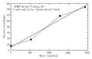
도 3은 종래 반도체 소자 제조방법에 있어서 웨이퍼 처리 수에 따른 로드락(loadlock)의 설퍼(sulfur) 농도 변화를 나타낸 도면.3 is a view showing a sulfur concentration change of a loadlock according to the number of wafer processes in a conventional semiconductor device manufacturing method.
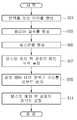
도 4는 본 발명에 따른 반도체 소자 제조방법의 제 1 실시 예를 나타낸 순서도.Figure 4 is a flow chart showing a first embodiment of a method of manufacturing a semiconductor device according to the present invention.
도 5는 본 발명에 따른 반도체 소자 제조방법의 제 2 실시 예를 나타낸 순서도.5 is a flow chart showing a second embodiment of a method of manufacturing a semiconductor device according to the present invention.
본 발명은 반도체 소자 제조방법에 관한 것이다.The present invention relates to a semiconductor device manufacturing method.
최근 들어 반도체 소자가 고집적화 되고 고속화 됨에 따라 RC 지연 개선을 위하여 듀얼 다마신(dual damascene)에 의한 구리 공정(Cu process)을 사용하는 추세를 보이고 있다.Recently, as semiconductor devices are becoming more integrated and faster, the Cu process using dual damascene has been used to improve the RC delay.
그러나 여전히 많은 반도체 소자 제조라인에서, 전기적 통로가 되는 금속 라 인(metal line)에는 알루미늄(Al)을 사용하고, 실리콘층(silincon layer)/금속층(matal layer)과 금속층의 연결(interconnect) 역할을 하는 컨택 및 비아(contact and via)에는 전기 저항이 낮고 스텝 커버리지(step coverage)가 좋은 텅스텐(W)을 사용하고 있다.However, in many semiconductor device manufacturing lines, aluminum (Al) is used for the metal line, which is an electrical path, and serves as a silicon layer / matal layer and metal layer interconnect. Contact and vias are made of tungsten (W), which has low electrical resistance and good step coverage.
한편, 컨택이나 비아에 증착된 텅스텐을 제거하고 플러그(plug)를 형성하기 위한 방법으로서, 통상적으로 CMP(Chemical Mechanical Polishing) 방법과 플라즈마(plasma)를 이용한 건식 식각(dry etch) 방법이 이용되고 있다.Meanwhile, as a method of removing tungsten deposited on a contact or via and forming a plug, a chemical mechanical polishing (CMP) method and a dry etching method using plasma are commonly used. .
상기 플라즈마를 이용한 건식 식각 방법을 이용하는 경우에는, 메인 에천트(main etchant)로서 텅스텐과 화학적 반응이 활발한 SF6 가스가 이용되며, 보조 가스로서 희석(dilution) 및 이온충격(ion bombardment)의 역할을 하는 Ar 가스가 이용된다. 이때, 다음 [반응식1]에 나타낸 바와 같은 반응이 진행된다.In the dry etching method using the plasma, SF6 gas having a chemical reaction with tungsten is used as a main etchant, and serves as a dilution and ion bombardment as an auxiliary gas. Ar gas is used. At this time, the reaction proceeds as shown in the following [Scheme 1].
그리고, 유전층(dielectric layer)과의 글루층(glue layer)으로서 Ti/TiN 층의 배리어 금속층(barrier metal layer)이 사용되고 있으며, 상기 플라즈마를 이용한 건식 식각 공정에서는 상기 배리어 금속과 텅스텐의 선택비(selectivity)가 상당히 중요한 공정변수가 된다. 이에 따라, 텅스텐과 배리어 금속 간의 선택비를 확보하기 위하여 웨이퍼 내에 텅스텐이 거의 제거되고, 배리어 금속이 드러나는 식각 단계에서도 상당량의 설퍼(sulfur)가 사용되어 진다.In addition, a barrier metal layer of a Ti / TiN layer is used as a glue layer with a dielectric layer, and a selectivity ratio between the barrier metal and tungsten in a dry etching process using the plasma is selected. ) Is a very important process variable. Accordingly, in order to secure the selectivity between tungsten and the barrier metal, a large amount of sulfur is used even in the etching step in which the tungsten is almost removed in the wafer and the barrier metal is exposed.
이러한 여건으로부터, 도 1 및 도 2에 나타낸 바와 같이, 웨이퍼 표면에 설퍼 기반 잔류물(sulfur-based residue)이 생성되는 문제점이 있다. 도 1 및 도 2는 종래 반도체 소자 제조방법에 있어서 설퍼 기반 잔류물이 생성된 것을 나타낸 사진이다.From these conditions, as shown in Figs. 1 and 2, there is a problem in that sulfur-based residues are generated on the wafer surface. 1 and 2 are photographs showing that sulfur-based residues are generated in the conventional semiconductor device manufacturing method.
따라서, 웨이퍼 위에 이러한 설퍼 기반 잔류물이 생성되는 것을 방지할 수 있는 방안에 대한 연구가 다양하게 진행되고 있다.Therefore, various studies have been conducted to prevent the formation of such sulfur-based residues on the wafer.
본 발명은 플라즈마를 이용한 건식 식각 공정을 통하여 컨택이나 비아에 증착된 텅스텐을 제거(W etch-back)하고 플러그(plug)를 형성함에 있어, 설퍼 기반 잔류물(sulfur-based residue)이 생성되는 것을 방지할 수 있는 반도체 소자 제조방법을 제공함에 그 목적이 있다.According to the present invention, sulfur-based residues are generated in the etching and removal of tungsten deposited on a contact or via through a dry etching process using plasma. Its purpose is to provide a method for manufacturing a semiconductor device that can be prevented.
상기 목적을 달성하기 위하여 본 발명에 따른 반도체 소자 제조방법의 제 1 실시 예는, 컨택홀 또는 비아홀을 형성하는 단계; 상기 결과물 위에 배리어 금속층을 형성하는 단계; 상기 배리어 금속층 위에 텅스텐층을 형성하며, 상기 컨택홀과 상기 비아홀을 텅스텐으로 채우는 단계; 산소 가스를 이용하여 공정챔버를 드라이 크리닝하는 단계; 플라즈마 가스를 이용하여 텅스텐 에치 백 공정을 수행하는 단계; 를 포함하는 점에 그 특징이 있다.In order to achieve the above object, a first embodiment of a method of manufacturing a semiconductor device according to the present invention may include forming a contact hole or a via hole; Forming a barrier metal layer on the resultant; Forming a tungsten layer on the barrier metal layer, and filling the contact hole and the via hole with tungsten; Dry cleaning the process chamber using oxygen gas; Performing a tungsten etch back process using plasma gas; Its features are to include.
또한 상기 목적을 달성하기 위하여 본 발명에 따른 반도체 소자 제조방법의 제 2 실시 예는, 컨택홀 또는 비아홀을 형성하는 단계; 상기 결과물 위에 배리어 금속층을 형성하는 단계; 상기 배리어 금속층 위에 텅스텐층을 형성하며, 상기 컨택홀과 상기 비아홀을 텅스텐으로 채우는 단계; 플라즈마 가스를 이용하여 상기 배리어 금속층이 노출되도록, 텅스텐 에치 백 공정의 메인식각(main etching) 공정을 수행하는 단계; 공정챔버 내의 분위기 가스를 외부로 배기시키는 펌핑공정을 수행하는 단계; 텅스텐 에치 백 공정의 과식각(over etching) 공정을 수행하는 단계; 를 포함하는 점에 그 특징이 있다.In addition, a second embodiment of the semiconductor device manufacturing method according to the present invention in order to achieve the above object, forming a contact hole or via hole; Forming a barrier metal layer on the resultant; Forming a tungsten layer on the barrier metal layer, and filling the contact hole and the via hole with tungsten; Performing a main etching process of a tungsten etch back process to expose the barrier metal layer using a plasma gas; Performing a pumping process of exhausting the atmosphere gas in the process chamber to the outside; Performing an over etching process of the tungsten etch back process; Its features are to include.
이와 같은 본 발명에 의하면, 플라즈마를 이용한 건식 식각 공정을 통하여 컨택이나 비아에 증착된 텅스텐을 제거하고 플러그(plug)를 형성함에 있어, 설퍼 기반 잔류물(sulfur-based residue)이 생성되는 것을 방지할 수 있는 장점이 있다.According to the present invention, in the dry etching process using plasma to remove the tungsten deposited on the contact or via and to form a plug, it is possible to prevent the formation of sulfur-based residue (sulfur-based residue) There are advantages to it.
이하, 첨부된 도면을 참조하여 본 발명에 따른 실시 예를 상세히 설명한다.Hereinafter, exemplary embodiments of the present invention will be described in detail with reference to the accompanying drawings.
먼저, 본 발명에서는 웨이퍼 표면에 설퍼 기반 잔류물(sulfur-based residue)이 생성되는 원인을 분석하기 위하여, 공정 조건을 변화시키면서 다음과 같은 웨이퍼 처리 공정을 수행하였다.First, in the present invention, in order to analyze the cause of the generation of sulfur-based residues (sulfur-based residue) on the wafer surface, the following wafer processing process was performed while changing the process conditions.
<웨이퍼 처리 공정><Wafer treatment process>
웨이퍼 → TEOS(Tetraethyl orthosilicate) 형성 → 금속층 형성 → 층간유전체층(IMD) 형성 → 비아홀 형성 → 배리어 금속층 형성 → 텅스텐층 형성(3.5K 또는 4.5K) → 스크러버(scrubber) 유무 → 텅스텐 에치 백 공정Wafer → TEOS (Tetraethyl orthosilicate) formation → metal layer formation → interlayer dielectric layer (IMD) formation → via hole formation → barrier metal layer formation → tungsten layer formation (3.5K or 4.5K) → presence of scrubber → tungsten etch back process
상기와 같은 처리순서에 따라 웨이퍼 처리 공정을 수행하였으며 [표1]에 나타낸 바와 같이 텅스텐 에치 백 공정의 이전 공정 조건(텅스텐층 두께 변경 및 스크러버 유무)에 따른 결함(defect) 발생 유무 및 시즈닝 매터리얼(seasoning material) 차이에 의한 공정챔버 조건 변화에 따른 효과를 확인하였다. 즉, 공정 조건을 변화시키면서 웨이퍼 표면에 설퍼 기반 잔류물(sulfur-based residue)이 생성되는 지의 여부를 확인하였다.The wafer processing process was carried out according to the processing procedure as described above. As shown in [Table 1], the presence of defects and the seasoning material according to the previous process conditions (tungsten layer thickness change and the presence of scrubber) of the tungsten etch back process (seasoning material) the effect of the change in the process chamber conditions due to the difference was confirmed. In other words, it was confirmed whether sulfur-based residues were formed on the wafer surface while changing the process conditions.
상기와 같이 공정 조건을 변화시키면서 설퍼 기반 잔류물의 생성 여부를 확인한 결과, 텅스텐층의 두께 및 스크러버 유무에 따른 결함 발생 경향성은 관측되지 아니 하였다. 또한, 시즈닝 매터리얼에 따른 공정챔버 조건 변화에 따른 결함 발생 경향성도 관측되지 아니 하였다.As a result of confirming whether the sulfur-based residues were produced while changing the process conditions as described above, the tendency of defect generation according to the thickness of the tungsten layer and the presence or absence of the scrubber was not observed. In addition, the tendency of defects to occur due to the change of process chamber condition according to seasoning material was not observed.
그러나 #5에서와 같이, TiN 웨이퍼로 Ar 가스 없이 단지 SF6 가스 만으로 플라즈마를 발생시켜 시즈닝을 진행하고, 일반적인 방법으로 텅스텐 에치 백을 진행한 후, RF 파워 인가없이 웨이퍼 위에 SF6 만을 흘려준 조건에서 설퍼 기반 잔류물이 발생되는 결함이 관측되었다. 또한, 재현성 여부를 실험한 #6의 결과에 나타낸 바와 같이, 동일한 공정조건에서는 동일하게 설퍼 기반 잔류물 생성이 관측되었다.However, as in # 5, the TiN wafer was subjected to seasoning by generating plasma with only SF6 gas without Ar gas, followed by tungsten etch back in a general manner, and then flowing SF6 only on the wafer without applying RF power. A defect was observed in which sulfur-based residues occurred. In addition, as shown in the results of # 6 experimenting with reproducibility, the production of sulfur-based residues was observed under the same process conditions.
그리고, 이러한 설퍼 기판 잔류물이 형성된 영역에 대한 TEM 분석 및 V-SEM 결과를 통해 이것이 텅스텐 에치 백 공정의 이전 공정이 아닌 텅스텐 에치 백 공정의 진행시에 발생된 것임을 확인할 수 있었다.TEM analysis and V-SEM results of the area where the sulfur substrate residues were formed, it was confirmed that this occurred during the progress of the tungsten etch back process rather than the previous process of the tungsten etch back process.
이러한 실험 결과를 기반으로 하여, 텅스텐 에치 백 공정을 수행함에 있어 배리어 금속층을 노출시키는 메인식각(main etching) 공정과 과식각(over etching) 공정 사이에 펌핑공정을 추가한 결과, 설퍼 기반 잔류물이 생성되는 것을 방지할 수 있었다.Based on the experimental results, a pumping process was added between the main etching process and the over etching process to expose the barrier metal layer in performing the tungsten etch back process. Could be prevented from being generated.
또한, 도 3에 나타낸 바와 같이, 처리되는 웨이퍼 수가 증가됨에 따라 로드락(loadlock)의 설퍼(sulfur) 농도가 증가되는 것을 관측할 수 있었고, 이러한 로드락의 설퍼 농도가 높은 경우에, 웨이퍼 위에 설퍼 기반 잔류물이 생성되는 빈도가 높다는 것을 확인할 수 있었다. 도 3은 종래 반도체 소자 제조방법에 있어서 웨이퍼 처리 수에 따른 로드락(loadlock)의 설퍼(sulfur) 농도 변화를 나타낸 도면이다.Also, as shown in FIG. 3, it was observed that the sulfur concentration of the loadlock increased as the number of wafers processed increased, and when the sulfur concentration of such loadlock was high, the sulfur on the wafer was increased. It was confirmed that the frequency of formation of the base residue was high. FIG. 3 is a view illustrating a change in sulfur concentration of a loadlock according to the number of wafer processes in a conventional method of manufacturing a semiconductor device.
이와 같은 관측결과로부터 웨이퍼 위에 설퍼 기반 잔류물이 생성되는 원인으로서 다음과 같은 분석이 제기될 수 있다.From these observations, the following analysis can be raised as a cause of the generation of sulfur-based residues on the wafer.
텅스텐 에치 백 공정시 발생되는 설퍼 기반 잔류물은, 배리어 금속층이 노출된 영역에서 플라즈마 상태로 해리된 설퍼가 배리어 금속층의 TiN과 거의 화학적(chemical) 반응을 하지 못하고 낮은 챔버 캐소드(chamber chthode) 온도(normal<30℃)에 의해 공정챔버의 배기라인(exhaust line)으로 펌핑(pumping)되지 못하고 그대로 응축(condensation)되어 웨이퍼 위에 잔존하게 된 것으로 분석된다.Sulfur-based residues generated during the tungsten etch back process are characterized by low chamber cathode temperature due to the dissociation of plasma dissociated into plasma in the region where the barrier metal layer is exposed, with little chemical reaction with TiN of the barrier metal layer. It is analyzed that it is not pumped into the exhaust line of the process chamber by normal <30 ° C., but is condensed as it is and remains on the wafer.
또한, 플라즈마 가스로 사용되는 SF6와 TiN과의 부산물(byproduct)인 TiFx가 설퍼 성분의 펌핑을 저해하는 요소로 작용되어 웨이퍼 위에 설퍼 기반 잔류물이 발생되는 것을 더 활성화 시킨 것으로 분석된다.In addition, TiFx, a by-product of SF6 and TiN used as plasma gas, acts as a factor that inhibits the pumping of the sulfur component, which further activates sulfur-based residues on the wafer.
이에 따라, 본 발명에서는 웨이퍼 위에 설퍼 기반 잔류물이 생성되는 것을 방지할 수 있도록 다음과 같은 반도체 소자 제조방법을 제시하고자 한다.Accordingly, the present invention is to provide a method for manufacturing a semiconductor device as follows to prevent the generation of sulfur-based residue on the wafer.
먼저, 도 4를 참조하여 본 발명의 제 1 실시 예에 따른 반도체 소자 제조방법을 설명해 보기로 한다. 도 4는 본 발명에 따른 반도체 소자 제조방법의 제 1 실시 예를 나타낸 순서도이다.First, a semiconductor device manufacturing method according to a first embodiment of the present invention will be described with reference to FIG. 4. 4 is a flowchart illustrating a first embodiment of a method of manufacturing a semiconductor device according to the present invention.
본 발명의 제 1 실시 예에 따른 반도체 소자 제조방법에 의하면, 도 4에 나타낸 바와 같이, 컨택홀 또는 비아홀을 형성하는 단계를 수행한다(단계 401).According to the method of manufacturing a semiconductor device according to the first embodiment of the present invention, as shown in FIG. 4, a step of forming a contact hole or a via hole is performed (step 401).
그리고, 상기 결과물 위에 배리어 금속층을 형성한다(단계 403). 여기서, 상기 배리어 금속층은 Ti/TiN 층으로 형성될 수 있다.Then, a barrier metal layer is formed on the resultant product (step 403). Here, the barrier metal layer may be formed of a Ti / TiN layer.
이어서 상기 배리어 금속층 위에 텅스텐층을 형성하며, 이때 상기 컨택홀과 비아홀은 텅스텐으로 채워지게 된다(단계 405).A tungsten layer is then formed over the barrier metal layer, wherein the contact and via holes are filled with tungsten (step 405).
본 발명에 의하면 상기 단계 405 이후에, 텅스텐 에치 백 공정을 바로 수행하는 것이 아니라 산소 가스를 이용하여 공정챔버에 대하여 드라이 크리닝을 수행한다(단계 407). 이와 같이 공정챔버에 대한 드라이 크리닝 공정을 수행함으로써, 공정챔버 내에 잔존하는 설퍼(sulfur) 성분을 제거할 수 있게 된다. 이에 따라 본 발명에 의하면, 다음에 진행될 텅스텐 에치 백 공정에서 웨이퍼 위에 설퍼 기반 잔류물이 생성되는 것을 방지할 수 있게 된다.According to the present invention, after
이후, 플라즈마 가스를 이용하여 텅스텐 에치 백 공정을 수행한다(단계 409). 여기서, 상기 플라즈마 가스는 메인 에천트(main etchant)로서 텅스텐과 화학적 반응이 활발한 SF6 가스가 이용되며, 보조 가스로서 희석(dilution) 및 이온충격(ion bombardment)의 역할을 하는 Ar 가스가 이용될 수 있다.Thereafter, a tungsten etch back process is performed using the plasma gas (step 409). In the plasma gas, SF6 gas which is active in chemical reaction with tungsten is used as a main etchant, and Ar gas, which serves as dilution and ion bombardment, may be used as an auxiliary gas. Can be.
상기 플라즈마 가스를 이용한 텅스텐 에치 백 공정은 상기 배리어 금속층을 노출시키는 메인식각(main etching) 공정과 추후 진행되는 과식각(over etching) 공정으로 나눌 수 있다. 이때, 상기 과식각 공정을 수행함에 있어, 식각을 위한 플라즈마 가스에 포함되는 SF6 의 가스 농도를 상기 메인식각 공정에 비하여 감소시키도록 제어할 수 있다. 이와 같이 상기 과식각 공정에서 SF6의 농도를 감소시킴으로써, 웨이퍼 위에 설퍼 기반 잔류물이 생성되는 것을 더욱 방지할 수 있게 된다.The tungsten etch back process using the plasma gas may be divided into a main etching process for exposing the barrier metal layer and an over etching process. At this time, in performing the over-etching process, the gas concentration of SF6 included in the plasma gas for etching may be controlled to be reduced compared to the main etching process. As such, by reducing the concentration of SF6 in the overetch process, it is possible to further prevent the generation of sulfur-based residues on the wafer.
그리고, 상기 텅스텐 에치 백 공정이 수행된 이후, 산소 가스를 이용하여 상기 공정챔버에 대하여 드라이 크리닝을 다시 수행한다(단계 411). 이와 같이 공정챔버에 대한 드라이 크리닝 공정을 다시 수행함으로써, 상기 공정챔버 내에 잔존할 수도 있는 설퍼(sulfur) 성분을 제거할 수 있게 된다.After the tungsten etch back process is performed, dry cleaning is again performed on the process chamber using oxygen gas (step 411). By performing the dry cleaning process for the process chamber in this way, it is possible to remove the sulfur (sulfur) component that may remain in the process chamber.
본 발명의 제 1 실시 예에 따른 반도체 소자 제조방법에 의하면, 산소 가스를 이용하여 공정챔버 내에 존재할 수 있는 설퍼 성분을 제거함으로써, 웨이퍼 위에 설퍼 기반 잔류물이 생성되는 것을 방지할 수 있게 된다.According to the semiconductor device manufacturing method according to the first embodiment of the present invention, by removing the sulfur component that may be present in the process chamber by using oxygen gas, it is possible to prevent the generation of sulfur-based residue on the wafer.
한편, 도 5는 본 발명에 따른 반도체 소자 제조방법의 제 2 실시 예를 나타낸 순서도이다.5 is a flowchart illustrating a second embodiment of a method of manufacturing a semiconductor device according to the present invention.
그러면, 도 5를 참조하여 본 발명의 제 2 실시 예에 따른 반도체 소자 제조방법에 대하여 설명해 보기로 한다.Next, a method of manufacturing a semiconductor device according to a second exemplary embodiment of the present invention will be described with reference to FIG. 5.
먼저, 컨택홀 또는 비아홀을 형성하고(단계 501), 그 결과물 위에 배리어 금속층을 형성한다(단계 503). 여기서, 상기 배리어 금속층은 Ti/TiN 층으로 형성될 수 있다.First, a contact hole or via hole is formed (step 501), and a barrier metal layer is formed on the resultant product (step 503). Here, the barrier metal layer may be formed of a Ti / TiN layer.
이어서 상기 배리어 금속층 위에 텅스텐층을 형성하며, 이때 상기 컨택홀과 비아홀은 텅스텐으로 채워지게 된다(단계 505).A tungsten layer is then formed over the barrier metal layer, wherein the contact and via holes are filled with tungsten (step 505).
그리고, 플라즈마 가스를 이용하여 상기 배리어 금속층이 노출되도록, 텅스텐 에치 백 공정의 메인식각(main etching) 공정을 수행한다(단계 507). 여기서, 상기 플라즈마 가스는 메인 에천트(main etchant)로서 텅스텐과 화학적 반응이 활발한 SF6 가스가 이용되며, 보조 가스로서 희석(dilution) 및 이온충격(ion bombardment)의 역할을 하는 Ar 가스가 이용될 수 있다.Then, a main etching process of the tungsten etch back process is performed to expose the barrier metal layer using plasma gas (step 507). In the plasma gas, SF6 gas which is active in chemical reaction with tungsten is used as a main etchant, and Ar gas, which serves as dilution and ion bombardment, may be used as an auxiliary gas. Can be.
본 발명에 의하면 상기 단계 507 이후에, 공정챔버 내의 분위기 가스를 외부로 배기시키는 펌핑공정을 수행한다(단계 509). 이로써, 공정챔버 내에 존재할 수 있는 설퍼 성분을 제거함으로써, 웨이퍼 위에 설퍼 기반 잔류물이 생성되는 것을 방지할 수 있게 된다.According to the present invention, after the
이어서, 플라즈마 가스를 이용하여 텅스텐 에치 백 공정의 과식각(over etching) 공정을 수행한다(단계 511). 이때, 상기 과식각 공정을 수행함에 있어, 식각을 위한 플라즈마 가스에 포함되는 SF6 의 가스 농도를 상기 메인식각 공정에 비하여 감소시키도록 제어할 수 있다. 이와 같이 상기 과식각 공정에서 SF6의 농도를 감소시킴으로써, 웨이퍼 위에 설퍼 기반 잔류물이 생성되는 것을 더욱 방지할 수 있게 된다.Subsequently, an over etching process of the tungsten etch back process is performed using the plasma gas (step 511). In this case, in performing the overetch process, the gas concentration of SF6 included in the plasma gas for etching may be controlled to be reduced compared to the main etching process. As such, by reducing the concentration of SF6 in the overetch process, it is possible to further prevent the generation of sulfur-based residues on the wafer.
또한, 상기 단계 507을 수행하기 이전 단계와 상기 단계 511을 수행한 이후 단계 중에서 적어도 하나의 단계에, 산소 가스를 이용하여 상기 공정챔버에 대하여 드라이 크리닝 공정을 수행하도록 할 수도 있다. 이와 같은 드라이 크리닝 공정을 추가하는 경우에는, 상기 공정챔버 내에 잔존할 수도 있는 설퍼(sulfur) 성분을 제거할 수 있게 되며, 웨이퍼 위에 설퍼 기반 잔류물이 생성되는 것을 더욱 방지할 수 있게 된다. 또한, 공정챔버의 캐소드 온도를 보다 높게 구현하는 경우에는, 상기 공정챔버 내의 설퍼가 더욱 원활하게 외부로 펌핑될 수 있게 된다.In addition, the dry cleaning process may be performed on the process chamber using oxygen gas in at least one of steps before performing
이상의 설명에서와 같이 본 발명에 따른 반도체 소자 제조방법에 의하면, 플라즈마를 이용한 건식 식각 공정을 통하여 컨택이나 비아에 증착된 텅스텐을 제거하고 플러그(plug)를 형성함에 있어, 설퍼 기반 잔류물(sulfur-based residue)이 생성되는 것을 방지할 수 있는 장점이 있다.According to the semiconductor device manufacturing method according to the present invention as described above, in the removal of tungsten deposited on the contact or via through a dry etching process using a plasma to form a plug, a sulfur-based residue (sulfur- based residue) can be prevented from forming.
Claims (8)
Translated fromKoreanPriority Applications (1)
| Application Number | Priority Date | Filing Date | Title |
|---|---|---|---|
| KR1020050100142AKR100698742B1 (en) | 2005-10-24 | 2005-10-24 | Semiconductor device manufacturing method |
Applications Claiming Priority (1)
| Application Number | Priority Date | Filing Date | Title |
|---|---|---|---|
| KR1020050100142AKR100698742B1 (en) | 2005-10-24 | 2005-10-24 | Semiconductor device manufacturing method |
Publications (1)
| Publication Number | Publication Date |
|---|---|
| KR100698742B1true KR100698742B1 (en) | 2007-03-23 |
Family
ID=41564183
Family Applications (1)
| Application Number | Title | Priority Date | Filing Date |
|---|---|---|---|
| KR1020050100142AExpired - Fee RelatedKR100698742B1 (en) | 2005-10-24 | 2005-10-24 | Semiconductor device manufacturing method |
Country Status (1)
| Country | Link |
|---|---|
| KR (1) | KR100698742B1 (en) |
Cited By (2)
| Publication number | Priority date | Publication date | Assignee | Title |
|---|---|---|---|---|
| CN117263248A (en)* | 2023-09-20 | 2023-12-22 | 湖北工业大学 | Sulfur fluorine recycling method and device for sulfur hexafluoride |
| CN117401718A (en)* | 2023-10-08 | 2024-01-16 | 湖北工业大学 | Novel method and device for converting sulfur hexafluoride in recycling mode |
Citations (3)
| Publication number | Priority date | Publication date | Assignee | Title |
|---|---|---|---|---|
| KR100254175B1 (en)* | 1997-06-30 | 2000-05-01 | 김영환 | Method of forming tungsten plug in semiconductor device |
| JP2002025991A (en)* | 2000-07-13 | 2002-01-25 | Fuji Electric Co Ltd | Plasma cleaning method and semiconductor device manufacturing method |
| KR100492914B1 (en)* | 2003-01-30 | 2005-05-31 | 동부아남반도체 주식회사 | Fabrication method of metal interconnection for semiconductor |
- 2005
- 2005-10-24KRKR1020050100142Apatent/KR100698742B1/ennot_activeExpired - Fee Related
Patent Citations (3)
| Publication number | Priority date | Publication date | Assignee | Title |
|---|---|---|---|---|
| KR100254175B1 (en)* | 1997-06-30 | 2000-05-01 | 김영환 | Method of forming tungsten plug in semiconductor device |
| JP2002025991A (en)* | 2000-07-13 | 2002-01-25 | Fuji Electric Co Ltd | Plasma cleaning method and semiconductor device manufacturing method |
| KR100492914B1 (en)* | 2003-01-30 | 2005-05-31 | 동부아남반도체 주식회사 | Fabrication method of metal interconnection for semiconductor |
Cited By (2)
| Publication number | Priority date | Publication date | Assignee | Title |
|---|---|---|---|---|
| CN117263248A (en)* | 2023-09-20 | 2023-12-22 | 湖北工业大学 | Sulfur fluorine recycling method and device for sulfur hexafluoride |
| CN117401718A (en)* | 2023-10-08 | 2024-01-16 | 湖北工业大学 | Novel method and device for converting sulfur hexafluoride in recycling mode |
Similar Documents
| Publication | Publication Date | Title |
|---|---|---|
| US7157351B2 (en) | Ozone vapor clean method | |
| US7341943B2 (en) | Post etch copper cleaning using dry plasma | |
| US8058178B1 (en) | Photoresist strip method for low-k dielectrics | |
| US7687446B2 (en) | Method of removing residue left after plasma process | |
| KR102703578B1 (en) | Process Integration Approach for Selective Metal Via Filling | |
| KR100500932B1 (en) | Method of dry cleaning and photoresist strip after via contact etching | |
| US6979633B2 (en) | Method of manufacturing semiconductor device | |
| JP2002009058A (en) | Etching method | |
| CN1316594C (en) | Method for making semiconductor device | |
| US6645852B1 (en) | Process for fabricating a semiconductor device having recess portion | |
| US7569481B2 (en) | Method for forming via-hole in semiconductor device | |
| US7253124B2 (en) | Process for defect reduction in electrochemical plating | |
| US6784109B2 (en) | Method for fabricating semiconductor devices including wiring forming with a porous low-k film and copper | |
| KR20080015931A (en) | Copper Peel-proof Semiconductor Device and Manufacturing Method Thereof | |
| KR100698742B1 (en) | Semiconductor device manufacturing method | |
| JP2010056574A (en) | Method of manufacturing semiconductor device | |
| JP2006165189A (en) | Method of manufacturing semiconductor device | |
| TWI467697B (en) | Method for fabricating an interconnection structure | |
| JP2015092548A (en) | Pre-cleaning of semiconductor structures | |
| US11688604B2 (en) | Method for using ultra thin ruthenium metal hard mask for etching profile control | |
| US6559047B1 (en) | Method of forming a metal interconnect that substantially reduces the formation of intermetallic residue regions | |
| US7442639B2 (en) | Method of forming plug of semiconductor device | |
| KR100564119B1 (en) | Metal wiring formation method of semiconductor device | |
| KR20100036449A (en) | Method of manufacturing semiconductor device | |
| KR100219061B1 (en) | Metal wiring formation method of semiconductor device |
Legal Events
| Date | Code | Title | Description |
|---|---|---|---|
| A201 | Request for examination | ||
| PA0109 | Patent application | St.27 status event code:A-0-1-A10-A12-nap-PA0109 | |
| PA0201 | Request for examination | St.27 status event code:A-1-2-D10-D11-exm-PA0201 | |
| PN2301 | Change of applicant | St.27 status event code:A-3-3-R10-R13-asn-PN2301 St.27 status event code:A-3-3-R10-R11-asn-PN2301 | |
| PN2301 | Change of applicant | St.27 status event code:A-3-3-R10-R13-asn-PN2301 St.27 status event code:A-3-3-R10-R11-asn-PN2301 | |
| D13-X000 | Search requested | St.27 status event code:A-1-2-D10-D13-srh-X000 | |
| D14-X000 | Search report completed | St.27 status event code:A-1-2-D10-D14-srh-X000 | |
| E902 | Notification of reason for refusal | ||
| PE0902 | Notice of grounds for rejection | St.27 status event code:A-1-2-D10-D21-exm-PE0902 | |
| E13-X000 | Pre-grant limitation requested | St.27 status event code:A-2-3-E10-E13-lim-X000 | |
| P11-X000 | Amendment of application requested | St.27 status event code:A-2-2-P10-P11-nap-X000 | |
| P13-X000 | Application amended | St.27 status event code:A-2-2-P10-P13-nap-X000 | |
| E701 | Decision to grant or registration of patent right | ||
| PE0701 | Decision of registration | St.27 status event code:A-1-2-D10-D22-exm-PE0701 | |
| GRNT | Written decision to grant | ||
| PR0701 | Registration of establishment | St.27 status event code:A-2-4-F10-F11-exm-PR0701 | |
| PR1002 | Payment of registration fee | St.27 status event code:A-2-2-U10-U11-oth-PR1002 Fee payment year number:1 | |
| PG1601 | Publication of registration | St.27 status event code:A-4-4-Q10-Q13-nap-PG1601 | |
| FPAY | Annual fee payment | Payment date:20100223 Year of fee payment:4 | |
| PR1001 | Payment of annual fee | St.27 status event code:A-4-4-U10-U11-oth-PR1001 Fee payment year number:4 | |
| LAPS | Lapse due to unpaid annual fee | ||
| PC1903 | Unpaid annual fee | St.27 status event code:A-4-4-U10-U13-oth-PC1903 Not in force date:20110316 Payment event data comment text:Termination Category : DEFAULT_OF_REGISTRATION_FEE | |
| PC1903 | Unpaid annual fee | St.27 status event code:N-4-6-H10-H13-oth-PC1903 Ip right cessation event data comment text:Termination Category : DEFAULT_OF_REGISTRATION_FEE Not in force date:20110316 | |
| P22-X000 | Classification modified | St.27 status event code:A-4-4-P10-P22-nap-X000 |