KR100698699B1 - Data driving circuit, light emitting display device and driving method thereof - Google Patents
Data driving circuit, light emitting display device and driving method thereofDownload PDFInfo
- Publication number
- KR100698699B1 KR100698699B1KR1020050070433AKR20050070433AKR100698699B1KR 100698699 B1KR100698699 B1KR 100698699B1KR 1020050070433 AKR1020050070433 AKR 1020050070433AKR 20050070433 AKR20050070433 AKR 20050070433AKR 100698699 B1KR100698699 B1KR 100698699B1
- Authority
- KR
- South Korea
- Prior art keywords
- voltage
- data
- transistor
- current
- supplied
- Prior art date
- Legal status (The legal status is an assumption and is not a legal conclusion. Google has not performed a legal analysis and makes no representation as to the accuracy of the status listed.)
- Expired - Lifetime
Links
Images


Classifications
- G—PHYSICS
- G09—EDUCATION; CRYPTOGRAPHY; DISPLAY; ADVERTISING; SEALS
- G09G—ARRANGEMENTS OR CIRCUITS FOR CONTROL OF INDICATING DEVICES USING STATIC MEANS TO PRESENT VARIABLE INFORMATION
- G09G3/00—Control arrangements or circuits, of interest only in connection with visual indicators other than cathode-ray tubes
- G09G3/20—Control arrangements or circuits, of interest only in connection with visual indicators other than cathode-ray tubes for presentation of an assembly of a number of characters, e.g. a page, by composing the assembly by combination of individual elements arranged in a matrix no fixed position being assigned to or needed to be assigned to the individual characters or partial characters
- G09G3/22—Control arrangements or circuits, of interest only in connection with visual indicators other than cathode-ray tubes for presentation of an assembly of a number of characters, e.g. a page, by composing the assembly by combination of individual elements arranged in a matrix no fixed position being assigned to or needed to be assigned to the individual characters or partial characters using controlled light sources
- G09G3/30—Control arrangements or circuits, of interest only in connection with visual indicators other than cathode-ray tubes for presentation of an assembly of a number of characters, e.g. a page, by composing the assembly by combination of individual elements arranged in a matrix no fixed position being assigned to or needed to be assigned to the individual characters or partial characters using controlled light sources using electroluminescent panels
- G09G3/32—Control arrangements or circuits, of interest only in connection with visual indicators other than cathode-ray tubes for presentation of an assembly of a number of characters, e.g. a page, by composing the assembly by combination of individual elements arranged in a matrix no fixed position being assigned to or needed to be assigned to the individual characters or partial characters using controlled light sources using electroluminescent panels semiconductive, e.g. using light-emitting diodes [LED]
- G09G3/3208—Control arrangements or circuits, of interest only in connection with visual indicators other than cathode-ray tubes for presentation of an assembly of a number of characters, e.g. a page, by composing the assembly by combination of individual elements arranged in a matrix no fixed position being assigned to or needed to be assigned to the individual characters or partial characters using controlled light sources using electroluminescent panels semiconductive, e.g. using light-emitting diodes [LED] organic, e.g. using organic light-emitting diodes [OLED]
- G09G3/3225—Control arrangements or circuits, of interest only in connection with visual indicators other than cathode-ray tubes for presentation of an assembly of a number of characters, e.g. a page, by composing the assembly by combination of individual elements arranged in a matrix no fixed position being assigned to or needed to be assigned to the individual characters or partial characters using controlled light sources using electroluminescent panels semiconductive, e.g. using light-emitting diodes [LED] organic, e.g. using organic light-emitting diodes [OLED] using an active matrix
- G09G3/3233—Control arrangements or circuits, of interest only in connection with visual indicators other than cathode-ray tubes for presentation of an assembly of a number of characters, e.g. a page, by composing the assembly by combination of individual elements arranged in a matrix no fixed position being assigned to or needed to be assigned to the individual characters or partial characters using controlled light sources using electroluminescent panels semiconductive, e.g. using light-emitting diodes [LED] organic, e.g. using organic light-emitting diodes [OLED] using an active matrix with pixel circuitry controlling the current through the light-emitting element
- G—PHYSICS
- G09—EDUCATION; CRYPTOGRAPHY; DISPLAY; ADVERTISING; SEALS
- G09G—ARRANGEMENTS OR CIRCUITS FOR CONTROL OF INDICATING DEVICES USING STATIC MEANS TO PRESENT VARIABLE INFORMATION
- G09G3/00—Control arrangements or circuits, of interest only in connection with visual indicators other than cathode-ray tubes
- G09G3/20—Control arrangements or circuits, of interest only in connection with visual indicators other than cathode-ray tubes for presentation of an assembly of a number of characters, e.g. a page, by composing the assembly by combination of individual elements arranged in a matrix no fixed position being assigned to or needed to be assigned to the individual characters or partial characters
- G09G3/22—Control arrangements or circuits, of interest only in connection with visual indicators other than cathode-ray tubes for presentation of an assembly of a number of characters, e.g. a page, by composing the assembly by combination of individual elements arranged in a matrix no fixed position being assigned to or needed to be assigned to the individual characters or partial characters using controlled light sources
- G09G3/30—Control arrangements or circuits, of interest only in connection with visual indicators other than cathode-ray tubes for presentation of an assembly of a number of characters, e.g. a page, by composing the assembly by combination of individual elements arranged in a matrix no fixed position being assigned to or needed to be assigned to the individual characters or partial characters using controlled light sources using electroluminescent panels
- G09G3/32—Control arrangements or circuits, of interest only in connection with visual indicators other than cathode-ray tubes for presentation of an assembly of a number of characters, e.g. a page, by composing the assembly by combination of individual elements arranged in a matrix no fixed position being assigned to or needed to be assigned to the individual characters or partial characters using controlled light sources using electroluminescent panels semiconductive, e.g. using light-emitting diodes [LED]
- G09G3/3208—Control arrangements or circuits, of interest only in connection with visual indicators other than cathode-ray tubes for presentation of an assembly of a number of characters, e.g. a page, by composing the assembly by combination of individual elements arranged in a matrix no fixed position being assigned to or needed to be assigned to the individual characters or partial characters using controlled light sources using electroluminescent panels semiconductive, e.g. using light-emitting diodes [LED] organic, e.g. using organic light-emitting diodes [OLED]
- G09G3/3275—Details of drivers for data electrodes
- G09G3/3283—Details of drivers for data electrodes in which the data driver supplies a variable data current for setting the current through, or the voltage across, the light-emitting elements
- G—PHYSICS
- G09—EDUCATION; CRYPTOGRAPHY; DISPLAY; ADVERTISING; SEALS
- G09G—ARRANGEMENTS OR CIRCUITS FOR CONTROL OF INDICATING DEVICES USING STATIC MEANS TO PRESENT VARIABLE INFORMATION
- G09G3/00—Control arrangements or circuits, of interest only in connection with visual indicators other than cathode-ray tubes
- G09G3/20—Control arrangements or circuits, of interest only in connection with visual indicators other than cathode-ray tubes for presentation of an assembly of a number of characters, e.g. a page, by composing the assembly by combination of individual elements arranged in a matrix no fixed position being assigned to or needed to be assigned to the individual characters or partial characters
- G09G3/22—Control arrangements or circuits, of interest only in connection with visual indicators other than cathode-ray tubes for presentation of an assembly of a number of characters, e.g. a page, by composing the assembly by combination of individual elements arranged in a matrix no fixed position being assigned to or needed to be assigned to the individual characters or partial characters using controlled light sources
- G09G3/30—Control arrangements or circuits, of interest only in connection with visual indicators other than cathode-ray tubes for presentation of an assembly of a number of characters, e.g. a page, by composing the assembly by combination of individual elements arranged in a matrix no fixed position being assigned to or needed to be assigned to the individual characters or partial characters using controlled light sources using electroluminescent panels
- G09G3/32—Control arrangements or circuits, of interest only in connection with visual indicators other than cathode-ray tubes for presentation of an assembly of a number of characters, e.g. a page, by composing the assembly by combination of individual elements arranged in a matrix no fixed position being assigned to or needed to be assigned to the individual characters or partial characters using controlled light sources using electroluminescent panels semiconductive, e.g. using light-emitting diodes [LED]
- G09G3/3208—Control arrangements or circuits, of interest only in connection with visual indicators other than cathode-ray tubes for presentation of an assembly of a number of characters, e.g. a page, by composing the assembly by combination of individual elements arranged in a matrix no fixed position being assigned to or needed to be assigned to the individual characters or partial characters using controlled light sources using electroluminescent panels semiconductive, e.g. using light-emitting diodes [LED] organic, e.g. using organic light-emitting diodes [OLED]
- G09G3/3275—Details of drivers for data electrodes
- G09G3/3291—Details of drivers for data electrodes in which the data driver supplies a variable data voltage for setting the current through, or the voltage across, the light-emitting elements
- G—PHYSICS
- G09—EDUCATION; CRYPTOGRAPHY; DISPLAY; ADVERTISING; SEALS
- G09G—ARRANGEMENTS OR CIRCUITS FOR CONTROL OF INDICATING DEVICES USING STATIC MEANS TO PRESENT VARIABLE INFORMATION
- G09G2300/00—Aspects of the constitution of display devices
- G09G2300/08—Active matrix structure, i.e. with use of active elements, inclusive of non-linear two terminal elements, in the pixels together with light emitting or modulating elements
- G09G2300/0809—Several active elements per pixel in active matrix panels
- G09G2300/0819—Several active elements per pixel in active matrix panels used for counteracting undesired variations, e.g. feedback or autozeroing
- G—PHYSICS
- G09—EDUCATION; CRYPTOGRAPHY; DISPLAY; ADVERTISING; SEALS
- G09G—ARRANGEMENTS OR CIRCUITS FOR CONTROL OF INDICATING DEVICES USING STATIC MEANS TO PRESENT VARIABLE INFORMATION
- G09G2300/00—Aspects of the constitution of display devices
- G09G2300/08—Active matrix structure, i.e. with use of active elements, inclusive of non-linear two terminal elements, in the pixels together with light emitting or modulating elements
- G09G2300/0809—Several active elements per pixel in active matrix panels
- G09G2300/0842—Several active elements per pixel in active matrix panels forming a memory circuit, e.g. a dynamic memory with one capacitor
- G09G2300/0852—Several active elements per pixel in active matrix panels forming a memory circuit, e.g. a dynamic memory with one capacitor being a dynamic memory with more than one capacitor
- G—PHYSICS
- G09—EDUCATION; CRYPTOGRAPHY; DISPLAY; ADVERTISING; SEALS
- G09G—ARRANGEMENTS OR CIRCUITS FOR CONTROL OF INDICATING DEVICES USING STATIC MEANS TO PRESENT VARIABLE INFORMATION
- G09G2300/00—Aspects of the constitution of display devices
- G09G2300/08—Active matrix structure, i.e. with use of active elements, inclusive of non-linear two terminal elements, in the pixels together with light emitting or modulating elements
- G09G2300/0809—Several active elements per pixel in active matrix panels
- G09G2300/0842—Several active elements per pixel in active matrix panels forming a memory circuit, e.g. a dynamic memory with one capacitor
- G09G2300/0861—Several active elements per pixel in active matrix panels forming a memory circuit, e.g. a dynamic memory with one capacitor with additional control of the display period without amending the charge stored in a pixel memory, e.g. by means of additional select electrodes
- G—PHYSICS
- G09—EDUCATION; CRYPTOGRAPHY; DISPLAY; ADVERTISING; SEALS
- G09G—ARRANGEMENTS OR CIRCUITS FOR CONTROL OF INDICATING DEVICES USING STATIC MEANS TO PRESENT VARIABLE INFORMATION
- G09G2310/00—Command of the display device
- G09G2310/02—Addressing, scanning or driving the display screen or processing steps related thereto
- G09G2310/0243—Details of the generation of driving signals
- G09G2310/0251—Precharge or discharge of pixel before applying new pixel voltage
- G—PHYSICS
- G09—EDUCATION; CRYPTOGRAPHY; DISPLAY; ADVERTISING; SEALS
- G09G—ARRANGEMENTS OR CIRCUITS FOR CONTROL OF INDICATING DEVICES USING STATIC MEANS TO PRESENT VARIABLE INFORMATION
- G09G2310/00—Command of the display device
- G09G2310/02—Addressing, scanning or driving the display screen or processing steps related thereto
- G09G2310/0264—Details of driving circuits
- G09G2310/027—Details of drivers for data electrodes, the drivers handling digital grey scale data, e.g. use of D/A converters
- G—PHYSICS
- G09—EDUCATION; CRYPTOGRAPHY; DISPLAY; ADVERTISING; SEALS
- G09G—ARRANGEMENTS OR CIRCUITS FOR CONTROL OF INDICATING DEVICES USING STATIC MEANS TO PRESENT VARIABLE INFORMATION
- G09G2310/00—Command of the display device
- G09G2310/02—Addressing, scanning or driving the display screen or processing steps related thereto
- G09G2310/0264—Details of driving circuits
- G09G2310/0289—Details of voltage level shifters arranged for use in a driving circuit
- G—PHYSICS
- G09—EDUCATION; CRYPTOGRAPHY; DISPLAY; ADVERTISING; SEALS
- G09G—ARRANGEMENTS OR CIRCUITS FOR CONTROL OF INDICATING DEVICES USING STATIC MEANS TO PRESENT VARIABLE INFORMATION
- G09G2320/00—Control of display operating conditions
- G09G2320/02—Improving the quality of display appearance
- G09G2320/0223—Compensation for problems related to R-C delay and attenuation in electrodes of matrix panels, e.g. in gate electrodes or on-substrate video signal electrodes
- G—PHYSICS
- G09—EDUCATION; CRYPTOGRAPHY; DISPLAY; ADVERTISING; SEALS
- G09G—ARRANGEMENTS OR CIRCUITS FOR CONTROL OF INDICATING DEVICES USING STATIC MEANS TO PRESENT VARIABLE INFORMATION
- G09G2320/00—Control of display operating conditions
- G09G2320/02—Improving the quality of display appearance
- G09G2320/0271—Adjustment of the gradation levels within the range of the gradation scale, e.g. by redistribution or clipping
- G09G2320/0276—Adjustment of the gradation levels within the range of the gradation scale, e.g. by redistribution or clipping for the purpose of adaptation to the characteristics of a display device, i.e. gamma correction
- G—PHYSICS
- G09—EDUCATION; CRYPTOGRAPHY; DISPLAY; ADVERTISING; SEALS
- G09G—ARRANGEMENTS OR CIRCUITS FOR CONTROL OF INDICATING DEVICES USING STATIC MEANS TO PRESENT VARIABLE INFORMATION
- G09G2320/00—Control of display operating conditions
- G09G2320/04—Maintaining the quality of display appearance
- G09G2320/043—Preventing or counteracting the effects of ageing
- G—PHYSICS
- G09—EDUCATION; CRYPTOGRAPHY; DISPLAY; ADVERTISING; SEALS
- G09G—ARRANGEMENTS OR CIRCUITS FOR CONTROL OF INDICATING DEVICES USING STATIC MEANS TO PRESENT VARIABLE INFORMATION
- G09G2330/00—Aspects of power supply; Aspects of display protection and defect management
- G09G2330/02—Details of power systems and of start or stop of display operation
Landscapes
- Engineering & Computer Science (AREA)
- Physics & Mathematics (AREA)
- Computer Hardware Design (AREA)
- General Physics & Mathematics (AREA)
- Theoretical Computer Science (AREA)
- Control Of Indicators Other Than Cathode Ray Tubes (AREA)
- Control Of El Displays (AREA)
- Electroluminescent Light Sources (AREA)
Abstract
Translated fromKoreanDescription
Translated fromKorean도 1은 종래의 발광 표시장치를 나타내는 도면이다.1 illustrates a conventional light emitting display device.
도 2는 본 발명의 실시예에 의한 발광 표시장치를 나타내는 도면이다.2 is a diagram illustrating a light emitting display device according to an exemplary embodiment of the present invention.
도 3은 도 2에 도시된 화소의 일례를 나타내는 회로도이다.3 is a circuit diagram illustrating an example of the pixel illustrated in FIG. 2.
도 4는 도 3에 도시된 화소의 구동방법을 나타내는 파형도이다.4 is a waveform diagram illustrating a method of driving the pixel illustrated in FIG. 3.
도 5는 도 2에 도시된 화소의 다른례를 나타내는 회로도이다.FIG. 5 is a circuit diagram illustrating another example of the pixel illustrated in FIG. 2.
도 6은 도 2에 도시된 데이터 구동회로의 제 1실시예를 나타내는 블록도이다.FIG. 6 is a block diagram showing a first embodiment of the data driving circuit shown in FIG.
도 7은 도 2에 도시된 데이터 구동회로의 제 2실시예를 나타내는 블록도이다.FIG. 7 is a block diagram showing a second embodiment of the data driving circuit shown in FIG.
도 8은 도 6에 도시된 전압 생성부, 디지털-아날로그 변환기, 제 1버퍼, 제 2버퍼, 스위칭부, 전류 싱크부 및 화소의 연결관계의 일례를 나타내는 도면이다.FIG. 8 is a diagram illustrating an example of a connection relationship between a voltage generator, a digital-to-analog converter, a first buffer, a second buffer, a switching unit, a current sinking unit, and a pixel illustrated in FIG. 6.
도 9는 도 8에 도시된 화소, 스위칭부 및 전류 싱크부의 구동방법을 나타내는 파형도이다.9 is a waveform diagram illustrating a driving method of the pixel, the switching unit, and the current sink unit illustrated in FIG. 8.
도 10은 도 8에 도시된 스위칭부의 다른례를 나타내는 도면이다.FIG. 10 is a diagram illustrating another example of the switching unit illustrated in FIG. 8.
도 11은 도 6에 도시된 전압 생성부, 디지털-아날로그 변환기, 제 1버퍼, 제 2버퍼, 스위칭부, 전류 싱크부 및 화소의 연결관계의 다른례를 나타내는 도면이다.FIG. 11 is a diagram illustrating another example of a connection relationship between a voltage generator, a digital-to-analog converter, a first buffer, a second buffer, a switching unit, a current sinking unit, and a pixel illustrated in FIG. 6.
도 12는 도 2에 도시된 데이터 구동회로의 제 3실시예를 나타내는 블록도이다.FIG. 12 is a block diagram showing a third embodiment of the data driving circuit shown in FIG.
도 13은 도 2에 도시된 데이터 구동회로의 제 4실시예를 나타내는 블록도이다.FIG. 13 is a block diagram showing a fourth embodiment of the data driving circuit shown in FIG.
도 14는 도 12에 도시된 전압 생성부, 디지털-아날로그 변환기, 승압부, 제 1버퍼, 제 2버퍼, 스위칭부, 전류 싱크부 및 화소의 연결관계의 일례를 나타내는 도면이다.FIG. 14 is a diagram illustrating an example of a connection relationship between a voltage generator, a digital-to-analog converter, a booster, a first buffer, a second buffer, a switching unit, a current sinker, and a pixel illustrated in FIG. 12.
도 15는 도 12에 도시된 전압 생성부, 디지털-아날로그 변환기, 승압부, 제 1버퍼, 제 2버퍼, 스위칭부, 전류 싱크부 및 화소의 연결관계의 다른례를 나타내는 도면이다.FIG. 15 is a diagram illustrating another example of a connection relationship between a voltage generator, a digital-to-analog converter, a booster, a first buffer, a second buffer, a switching unit, a current sinker, and a pixel illustrated in FIG. 12.
도 16은 도 2에 도시된 데이터 구동회로의 제 5실시예를 나타내는 블록도이다.FIG. 16 is a block diagram showing a fifth embodiment of the data driving circuit shown in FIG.
도 17은 도 16에 도시된 전압 생성부, 디지털-아날로그 변환기, 승압부, 제 1버퍼, 제 2버퍼, 스위칭부, 전류 싱크부 및 화소의 연결관계의 일례를 나타내는 도면이다.FIG. 17 is a diagram illustrating an example of a connection relationship between a voltage generator, a digital-to-analog converter, a booster, a first buffer, a second buffer, a switching unit, a current sinker, and a pixel illustrated in FIG. 16.
<도면의 주요 부분에 대한 부호의 설명><Explanation of symbols for the main parts of the drawings>
110 : 주사 구동부120 : 데이터 구동부110: scan driver 120: data driver
130 : 화소부140 : 화소130: pixel portion 140: pixel
142 : 화소회로150 : 타이밍 제어부142: pixel circuit 150: timing controller
200 : 데이터 구동회로210 : 쉬프트 레지스터부200: data driving circuit 210: shift register section
220 : 샘플링 래치부230 : 홀딩 래치부220: sampling latch portion 230: holding latch portion
240,400 : 감마 전압부250 : 디지털-아날로그 변환부240,400: gamma voltage unit 250: digital-analog converter
260,270 : 버퍼부280 : 전류 공급부260,270: buffer unit 280: current supply unit
290 : 선택부300 : 레벨 쉬프터부290: selection unit 300: level shifter unit
410,420 : 승압블록410,420: Boosting block
본 발명은 데이터 구동회로와 이를 이용한 발광 표시장치 및 그의 구동방법에 관한 것으로, 특히 균일한 휘도의 영상을 표시할 수 있도록 한 데이터 구동회로와 이를 이용한 발광 표시장치 및 그의 구동방법에 관한 것이다.BACKGROUND OF THE
최근, 음극선관(Cathode Ray Tube)의 단점인 무게와 부피를 줄일 수 있는 각종 평판 표시장치들이 개발되고 있다. 평판 표시장치로는 액정 표시장치(Liquid Crystal Display), 전계방출 표시장치(Field Emission Display), 플라즈마 표시패널(Plasma Display Panel) 및 발광 표시장치(Light Emitting Display) 등이 있다.Recently, various flat panel displays have been developed to reduce weight and volume, which are disadvantages of cathode ray tubes. The flat panel display includes a liquid crystal display, a field emission display, a plasma display panel, a light emitting display, and the like.
평판 표시장치 중 발광 표시장치는 전자와 정공의 재결합에 의하여 빛을 발 생하는 발광소자를 이용하여 영상을 표시한다. 이러한, 발광 표시장치는 빠른 응답속도를 가짐과 동시에 낮은 소비전력으로 구동되는 장점이 있다.Among the flat panel display devices, the light emitting display device displays an image using a light emitting device that emits light by recombination of electrons and holes. Such a light emitting display device has an advantage in that it has a fast response speed and is driven with low power consumption.
도 1은 종래의 발광 표시장치를 나타내는 도면이다.1 illustrates a conventional light emitting display device.
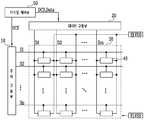
도 1을 참조하면, 종래의 발광 표시장치는 주사선들(S1 내지 Sn) 및 데이터선들(D1 내지 Dm)과 접속된 복수의 화소들(40)을 포함하는 화소부(30)와, 주사선들(S1 내지 Sn)을 구동하기 위한 주사 구동부(10)와, 데이터선들(D1 내지 Dm)을 구동하기 위한 데이터 구동부(20)와, 주사 구동부(10) 및 데이터 구동부(20)를 제어하기 위한 타이밍 제어부(50)를 구비한다.Referring to FIG. 1, a conventional light emitting display device includes a
타이밍 제어부(50)는 외부로부터 공급되는 동기신호들에 대응하여 데이터 구동제어신호(DCS) 및 주사 구동제어신호(SCS)를 생성한다. 타이밍 제어부(50)에서 생성된 데이터 구동제어신호(DCS)는 데이터 구동부(20)로 공급되고, 주사 구동제어신호(SCS)는 주사 구동부(10)로 공급된다. 그리고, 타이밍 제어부(50)는 외부로부터 공급되는 데이터(Data)를 데이터 구동부(20)로 공급한다.The
주사 구동부(10)는 타이밍 제어부(50)로부터 주사 구동제어신호(SCS)를 공급받는다. 주사 구동제어신호(SCS)를 공급받은 주사 구동부(10)는 주사신호를 생성하고, 생성된 주사신호를 주사선들(S1 내지 Sn)로 순차적으로 공급한다.The
데이터 구동부(20)는 타이밍 제어부(50)로부터 데이터 구동제어신호(DCS)를 공급받는다. 데이터 구동제어신호(DCS)를 공급받은 데이터 구동부(20)는 데이터신호를 생성하고, 생성된 데이터신호를 주사신호와 동기되도록 데이터선들(D1 내지 Dm)로 공급한다.The
화소부(30)는 외부로부터 제 1전원(ELVDD) 및 제 2전원(ELVSS)을 공급받아 각각의 화소들(40)로 공급한다. 제 1전원(ELVDD) 및 제 2전원(ELVSS)을 공급받은 화소들(40) 각각은 데이터신호에 대응하여 제 1전원(ELVDD)으로부터 발광소자를 경유하여 제 2전원(ELVSS)으로 흐르는 전류를 제어함으로써 데이터신호에 대응되는 빛을 생성한다.The
즉, 종래의 발광 표시장치에서 화소들(40) 각각은 데이터신호에 대응되어 소정 휘도의 빛을 생성한다. 하지만, 종래에는 화소들(40) 각각에 포함되는 트랜지스터들의 문턱전압 불균일 및 전자 이동도(electron mobility)의 편차에 의하여 원하는 휘도의 영상을 표시하지 못하는 문제점이 있다. 실제로, 화소들(40) 각각에 포함되는 트랜지스터들의 문턱전압은 화소들(40)에 포함되는 화소회로의 구조를 제어함으로써 어느 정도 보상할 수 있으나, 전자 이동도의 편차는 보상되지 못한다. 따라서, 전자 이동도의 편차와 무관하게 균일한 화상을 표시할 수 있는 발광 표시장치가 요구되고 있다.That is, in the conventional light emitting display device, each of the
따라서, 본 발명의 목적은 균일한 휘도의 영상을 표시할 수 있도록 한 데이터 구동회로와 이를 이용한 발광 표시장치 및 그의 구동방법을 제공하는 것이다.Accordingly, an object of the present invention is to provide a data driving circuit, a light emitting display device using the same, and a method of driving the same, capable of displaying an image of uniform luminance.
상기 목적을 달성하기 위하여, 본 발명의 제 1측면은 데이터선에서 소정의 전류가 흐르도록 제어하는 적어도 하나의 전류 싱크부와, 상기 소정의 전류가 흐를 때 생성되는 보상전압을 이용하여 계조전압들의 전압값을 재설정하는 적어도 하나의 전압 생성부와, 외부로부터 공급되는 데이터의 비트값에 대응하여 상기 계조전압들 중 어느 하나의 계조전압을 데이터신호로 선택하는 적어도 하나의 디지털-아날로그 변환기와, 상기 데이터신호의 전압값을 승압하기 위한 적어도 하나의 승압부와, 상기 승압된 데이터신호를 상기 데이터선으로 공급하기 위한 적어도 하나의 스위칭부를 구비하는 데이터 구동회로를 제공한다.In order to achieve the above object, the first aspect of the present invention provides a method for controlling the flow of a predetermined current through a data line, and using a compensation voltage generated when the predetermined current flows. At least one voltage generator for resetting a voltage value, at least one digital-analog converter for selecting one of the gray voltages as a data signal in response to a bit value of data supplied from the outside; A data driving circuit includes at least one boosting unit for boosting a voltage value of a data signal, and at least one switching unit for supplying the boosted data signal to the data line.
바람직하게, 상기 승압부는 상기 데이터선의 부하에 의하여 발생되는 상기 보상전압의 전압강하 전압에 대응하여 상기 데이터신호의 전압값을 승압한다. 상기 데이터선은 화소와 접속되며 상기 화소는 기준전원과 상기 승압된 데이터신호의 전압차를 이용하여 전압을 충전하고, 충전된 전압에 대응하여 제 1전원으로부터 발광소자로 흐르는 전류를 제어한다. 상기 승압부는 상기 기준전원과 상기 기준전원에서 상기 전압강하 전압을 감한 제 2기준전원을 입력받고, 상기 기준전원과 상기 제 2기준전원의 차전압만큼 상기 데이터신호의 전압을 승압한다. 상기 전압 생성부는 상기 제 2기준전원을 공급받는 제 1측단자와 상기 보상전압을 공급받는 제 2측단자 사이에 설치되어 상기 계조전압들을 생성하기 위한 복수의 분압저항들을 구비한다.Preferably, the boosting unit boosts the voltage value of the data signal in response to the voltage drop voltage of the compensation voltage generated by the load of the data line. The data line is connected to a pixel, and the pixel charges a voltage using a voltage difference between a reference power supply and the boosted data signal, and controls a current flowing from the first power supply to the light emitting device in response to the charged voltage. The boosting unit receives a second reference power obtained by subtracting the voltage drop voltage from the reference power supply and the reference power supply, and boosts the voltage of the data signal by the difference voltage between the reference power supply and the second reference power supply. The voltage generator includes a plurality of voltage divider resistors disposed between the first terminal receiving the second reference power and the second terminal receiving the compensation voltage to generate the gray scale voltages.
본 발명의 제 2측면은 데이터선과 접속된 화소로부터 소정의 전류를 공급받고, 공급받은 전류에 대응하는 보상전압을 생성하기 위한 적어도 하나의 전류 싱크부와; 상기 보상전압의 전압값을 승압하기 위한 적어도 하나 이상의 승압부와; 상기 승압된 보상전압을 이용하여 계조전압들의 전압값을 재설정하는 적어도 하나의 전압 생성부와; 외부로부터 공급되는 데이터의 비트값에 대응하여 상기 계조전압들 중 어느 하나의 계조전압을 데이터신호로 선택하는 적어도 하나의 디지털-아날로그 변환기와; 상기 데이터신호를 상기 데이터선으로 공급하기 위한 적어도 하나의 스위칭부를 구비한다.The second aspect of the present invention includes at least one current sink for receiving a predetermined current from a pixel connected to the data line and generating a compensation voltage corresponding to the supplied current; At least one booster for boosting the voltage value of the compensation voltage; At least one voltage generator configured to reset voltage values of gray voltages using the boosted compensation voltage; At least one digital-analog converter that selects one of the gray voltages as a data signal in response to a bit value of data supplied from the outside; At least one switching unit for supplying the data signal to the data line.
바람직하게, 상기 승압부는 상기 데이터선의 부하에 의하여 발생되는 상기 보상전압의 전압강하 전압만큼 상기 보상전압의 전압값을 승압한다. 상기 화소는 기준전원과 상기 데이터신호의 전압차를 이용하여 전압을 충전하고, 충전된 전압에 대응하여 제 1전원으로부터 발광소자로 흐르는 전류를 제어한다. 상기 승압부는 상기 기준전원과 상기 기준전원에서 상기 전압강하 전압을 감한 제 2기준전원을 입력받고, 상기 기준전원과 상기 제 2기준전원의 차만큼 상기 보상전압의 전압값을 승압한다.Preferably, the booster boosts the voltage value of the compensation voltage by the voltage drop voltage of the compensation voltage generated by the load of the data line. The pixel charges a voltage using a voltage difference between a reference power supply and the data signal, and controls a current flowing from the first power supply to the light emitting device in response to the charged voltage. The boosting unit receives a second reference power obtained by subtracting the voltage drop voltage from the reference power supply and the reference power supply, and boosts the voltage value of the compensation voltage by the difference between the reference power supply and the second reference power supply.
본 발명의 제 3측면은 주사선들, 데이터선들 및 발광 제어선들과 접속되도록 위치되는 복수의 화소를 포함하는 화소부와; 상기 주사선들로 주사신호를 순차적으로 공급하며, 상기 발광 제어선들로 발광 제어신호를 순차적으로 공급하기 위한 주사 구동부와; 상기 데이터선들로 데이터신호를 공급하기 위한 청구항 제 1항 내지 청구항 제 28항 중 어느 한 항에 기재된 적어도 하나의 데이터 구동회로를 구비하는 발광 표시장치를 제공한다.A third aspect of the present invention includes a pixel portion including a plurality of pixels positioned to be connected to scan lines, data lines and emission control lines; A scan driver for sequentially supplying scan signals to the scan lines, and sequentially supplying emission control signals to the emission control lines; A light emitting display device comprising at least one data driving circuit according to any one of
본 발명의 제 4측면은 (a) 화소와 접속된 데이터선에서 소정의 전류가 흐르 도록 제어하는 단계와, (b) 상기 소정의 전류에 대응되는 보상전압을 생성하는 단계와, (c) 상기 보상전압을 이용하여 계조전압들의 전압값을 제어하는 단계와, (d) 외부로부터 공급되는 데이터의 비트값에 대응하여 상기 계조전압들 중 어느 하나의 계조전압을 데이터신호로 선택하는 단계와, (e) 상기 데이터신호의 전압값을 승압하여 상기 데이터선으로 공급하는 단계를 포함하는 발광 표시장치의 구동방법을 제공한다. According to a fourth aspect of the present invention, (a) controlling a predetermined current to flow in a data line connected to a pixel, (b) generating a compensation voltage corresponding to the predetermined current, and (c) the Controlling a voltage value of the gray voltages using a compensation voltage, (d) selecting one of the gray voltages as a data signal in response to a bit value of data supplied from the outside; and e) boosting the voltage value of the data signal and supplying the voltage to the data line.
바람직하게, 상기 (a)단계에서는 상기 화소들이 최대 휘도로 발광할 때 흐르는 전류와 동일한 전류가 상기 데이터선에 흐르도록 제어한다. 상기 (e)단계에서는 상기 데이터선이 부하에 의하여 발생되는 상기 보상전압의 전압강하 전압만큼 상기 데이터신호의 전압을 승압한다.Preferably, in the step (a), the same current as that flowing when the pixels emit light at the maximum luminance is controlled to flow in the data line. In the step (e), the data line boosts the voltage of the data signal by the voltage drop voltage of the compensation voltage generated by the load.
본 발명의 제 5측면은 (a) 화소와 접속된 데이터선에서 소정의 전류가 흐르도록 제어하는 단계와, (b) 상기 소정의 전류에 대응하여 생성되는 보상전압을 승압하는 단계와, (c) 상기 승압된 보상전압을 이용하여 계조전압들의 전압값을 제어하는 단계와, (d) 외부로부터 공급되는 데이터의 비트값에 대응하여 상기 계조전압들 중 어느 하나의 계조전압을 데이터신호로 선택하는 단계와, (e) 상기 데이터신호를 상기 데이터선을 경유하여 상기 화소로 공급하는 단계를 포함하는 발광 표시장치의 구동방법을 제공한다.The fifth aspect of the present invention provides the steps of (a) controlling a predetermined current to flow in a data line connected to the pixel, (b) boosting a compensation voltage generated corresponding to the predetermined current, and (c Controlling the voltage values of the gray voltages using the boosted compensation voltage; and (d) selecting one of the gray voltages as a data signal in response to a bit value of data supplied from the outside. And (e) supplying the data signal to the pixel via the data line.
바람직하게, 상기 (a)단계에서는 상기 화소들이 최대 휘도로 발광할 때 흐르는 전류와 동일한 전류가 상기 데이터선에 흐르도록 제어한다. 상기 (b)단계에서는 상기 데이터선이 부하에 의하여 발생되는 전압강하 전압만큼 상기 보상전압의 전압 을 승압한다.Preferably, in the step (a), the same current as that flowing when the pixels emit light at the maximum luminance is controlled to flow in the data line. In the step (b), the data line boosts the voltage of the compensation voltage by the voltage drop voltage generated by the load.
이하, 본 발명이 속하는 기술분야에서 통상의 지식을 가진 자가 본 발명을 용이하게 실시할 수 있는 바람직한 실시 예를 첨부된 도 2 내지 도 17을 참조하여 상세히 설명하면 다음과 같다.Hereinafter, preferred embodiments of the present invention may be easily implemented by those skilled in the art with reference to FIGS. 2 to 17 as follows.
도 2는 본 발명의 실시예에 의한 발광 표시장치를 나타내는 도면이다.2 is a diagram illustrating a light emitting display device according to an exemplary embodiment of the present invention.
도 2를 참조하면, 본 발명의 실시예에 의한 발광 표시장치는 주사선들(S1 내지 Sn), 발광 제어선들(E1 내지 En) 및 데이터선들(D1 내지 Dm)과 접속되는 복수의 화소들(140)을 포함하는 화소부(130)와, 주사선들(S1 내지 Sn) 및 발광 제어선들(E1 내지 En)을 구동하기 위한 주사 구동부(110)와, 데이터선들(D1 내지 Dm)을 구동하기 위한 데이터 구동부(120)와, 주사 구동부(110) 및 데이터 구동부(120)를 제어하기 위한 타이밍 제어부(150)를 구비한다.2, a light emitting display device according to an exemplary embodiment of the present invention includes a plurality of
화소부(130)는 주사선들(S1 내지 Sn), 발광 제어선들(E1 내지 En) 및 데이터선들(D1 내지 Dm)에 의하여 구획된 영역에 형성되는 화소들(140)을 구비한다. 화소들(140)은 외부로부터 제 1전원(ELVDD), 제 2전원(ELVSS) 및 기준전원(Vref)을 공급받는다. 기준전원(Vref)을 공급받은 화소들(140) 각각은 기준전원(Vref)과 제 1전원(ELVDD)의 차값을 이용하여 제 1전원(ELVDD)의 전압강하를 보상한다. 그리고, 화소들(140) 각각은 데이터신호에 대응하여 제 1전원(ELVDD)으로부터 발광소자 (미도시)를 경유하여 제 2전원(ELVSS)으로 소정의 전류를 공급한다. 이를 위하여, 화소들(140) 각각은 도 3 또는 도 5와 같이 구성될 수 있다. 도 3 또는 도 5에 도시된 화소(140)의 상세한 구조는 후술하기로 한다.The
타이밍 제어부(150)는 외부로부터 공급되는 동기신호들에 대응하여 데이터 구동제어신호(DCS) 및 주사 구동제어신호(SCS)를 생성한다. 타이밍 제어부(150)에서 생성된 데이터 구동제어신호(DCS)는 데이터 구동부(120)로 공급되고, 주사 구동제어신호(SCS)는 주사 구동부(110)로 공급된다. 그리고, 타이밍 제어부(150)는 외부로부터 공급되는 데이터(Data)를 데이터 구동부(120)로 공급한다.The
주사 구동부(110)는 주사 구동제어신호(SCS)를 공급받는다. 주사 구동제어신호(SCS)를 공급받은 주사 구동부(110)는 주사선들(S1 내지 Sn)로 주사신호를 순차적으로 공급한다. 그리고, 주사 구동제어신호(SCS)를 공급받은 주사 구동부(110)는 발광 제어선들(E1 내지 En)로 발광 제어신호를 순차적으로 공급한다. 여기서, 발광 제어신호는 2개의 주사신호와 중첩되도록 공급된다. 이를 위하여, 발광 제어신호의 폭은 주사신호의 폭과 같거나 넓게 설정된다.The
데이터 구동부(120)는 타이밍 제어부(150)로부터 데이터 구동제어신호(DCS)를 공급받는다. 데이터 구동제어신호(DCS)를 공급받은 데이터 구동부(120)는 데이터신호를 생성하고, 생성된 데이터신호를 데이터선들(D1 내지 Dm)로 공급한다. 여기서, 데이터 구동부(120)는 1수평기간(1H)중 제 1기간 동안 데이터선들(D1 내지 Dm)로 소정의 전류를 공급하고, 1수평기간(1H)중 제 1기간을 제외한 제 2기간 동안 데이터선들(D1 내지 Dm)로 소정의 전압을 공급한다. 이를 위해, 데이터 구동부 (120)는 적어도 하나의 데이터 구동회로(200)를 구비한다. 이후, 설명의 편의성을 위하여 제 2기간 동안 데이터선들(D1 내지 Dm)로 공급되는 전압을 데이터신호라 하기로 한다.The
도 3은 도 2에 도시된 화소의 일례를 나타내는 도면이다. 도 3에서는 설명의 편의성을 위하여 제 m데이터선(Dm), 제 n-1 및 제 n주사선(Sn-1, Sn) 및 제 n발광 제어선(En)과 접속된 화소를 도시하기로 한다.3 is a diagram illustrating an example of a pixel illustrated in FIG. 2. In FIG. 3, pixels connected to the m-th data line Dm, the n-th and n-th scan lines Sn-1 and Sn, and the n-th emission control line En are shown for convenience of description.
도 3을 참조하면, 본 발명의 화소(140)는 발광소자(OLED), 발광소자(OLED)로 전류를 공급하기 위한 화소회로(142)를 구비한다.Referring to FIG. 3, the
발광소자(OLED)는 화소회로(142)로부터 공급되는 전류에 대응하여 소정 색의 빛을 생성한다. 이를 위하여, 발광소자(OLED)는 유기물질, 인광물질 및/또는 무기물질 등으로 형성된다.The light emitting device OLED generates light of a predetermined color in response to a current supplied from the
화소회로(142)는 제 n-1주사선(Sn-1)(이전 주사선)으로 주사신호가 공급될 때 제 1전원(ELVDD)의 전압강하와 제 4트랜지스터(M4)의 문턱전압을 보상하고, 제 n주사선(Sn)(현재 주사선)으로 주사신호가 공급될 때 데이터신호에 대응되는 전압을 충전한다. 이를 위해, 화소회로(142)는 제 1 내지 제 6트랜지스터(M1 내지 M6)와, 제 1커패시터(C1) 및 제 2커패시터(C2)를 구비한다.The
제 1트랜지스터(M1)의 제 1전극은 데이터선(Dm)에 접속되고, 제 2전극은 제 1노드(N1)에 접속된다. 그리고, 제 1트랜지스터(M1)의 게이트전극은 제 n주사선(Sn)에 접속된다. 이와 같은 제 1트랜지스터(M1)는 제 n주사선(Sn)으로 주사신호 가 공급될 때 턴-온되어 데이터선(Dm)과 제 1노드(N1)를 전기적으로 접속시킨다.The first electrode of the first transistor M1 is connected to the data line Dm, and the second electrode is connected to the first node N1. The gate electrode of the first transistor M1 is connected to the nth scan line Sn. The first transistor M1 is turned on when a scan signal is supplied to the nth scan line Sn to electrically connect the data line Dm and the first node N1.
제 2트랜지스터(M2)의 제 1전극은 데이터선(Dm)에 접속되고, 제 2전극은 제 4트랜지스터(M4)의 제 2전극에 접속된다. 그리고, 제 2트랜지스터(M2)의 게이트전극은 제 n주사선(Sn)에 접속된다. 이와 같은 제 2트랜지스터(M2)는 제 n주사선(Sn)으로 주사신호가 공급될 때 턴-온되어 데이터선(Dm)과 제 4트랜지스터(M4)의 제 2전극을 전기적으로 접속시킨다.The first electrode of the second transistor M2 is connected to the data line Dm, and the second electrode is connected to the second electrode of the fourth transistor M4. The gate electrode of the second transistor M2 is connected to the nth scan line Sn. The second transistor M2 is turned on when a scan signal is supplied to the nth scan line Sn to electrically connect the data line Dm and the second electrode of the fourth transistor M4.
제 3트랜지스터(M3)의 제 1전극은 기준전원(Vref)에 접속되고, 제 2전극은 제 1노드(N1)에 접속된다. 그리고, 제 3트랜지스터(M3)의 게이트전극은 제 n-1주사선(Sn-1)에 접속된다. 이와 같은 제 3트랜지스터(M3)는 제 n-1주사선(Sn-1)으로 주사신호가 공급될 때 턴-온되어 기준전원(Vref)과 제 1노드(N1)를 전기적으로 접속시킨다.The first electrode of the third transistor M3 is connected to the reference power supply Vref, and the second electrode is connected to the first node N1. The gate electrode of the third transistor M3 is connected to the n-1 th scan line Sn-1. The third transistor M3 is turned on when the scan signal is supplied to the n-1 th scan line Sn-1 to electrically connect the reference power supply Vref and the first node N1.
제 4트랜지스터(M4)의 제 1전극은 제 1전원(ELVDD)에 접속되고, 제 2전극은 제 6트랜지스터(M6)의 제 1전극에 접속된다. 그리고, 제 4트랜지스터(M4)의 게이트전극은 제 2노드(N2)에 접속된다. 이와 같은 제 4트랜지스터(M4)는 제 2노드(N2)에 인가되는 전압, 즉 제 1커패시터(C1) 및 제 2커패시터(C2)에 충전된 전압에 대응되는 전류를 제 6트랜지스터(M6)의 제 1전극으로 공급한다.The first electrode of the fourth transistor M4 is connected to the first power source ELVDD, and the second electrode is connected to the first electrode of the sixth transistor M6. The gate electrode of the fourth transistor M4 is connected to the second node N2. As such, the fourth transistor M4 receives a current corresponding to a voltage applied to the second node N2, that is, a voltage charged in the first capacitor C1 and the second capacitor C2, of the sixth transistor M6. Supply to the first electrode.
제 5트랜지스터(M5)의 제 2전극은 제 2노드(N2)에 접속되고, 제 1전극은 제 4트랜지스터(M4)의 제 2전극에 접속된다. 그리고, 제 5트랜지스터(M5)의 게이트전극은 제 n-1주사선(Sn-1)에 접속된다. 이와 같은 제 5트랜지스터(M5)는 제 n-1주사선(Sn-1)으로 주사신호가 공급될 때 턴-온되어 제 4트랜지스터(M4)를 다이오드 형태로 접속시킨다.The second electrode of the fifth transistor M5 is connected to the second node N2, and the first electrode is connected to the second electrode of the fourth transistor M4. The gate electrode of the fifth transistor M5 is connected to the n-1 th scan line Sn-1. The fifth transistor M5 is turned on when the scan signal is supplied to the n-th scan line Sn-1 to connect the fourth transistor M4 in the form of a diode.
제 6트랜지스터(M6)의 제 1전극은 제 4트랜지스터(M4)의 제 2전극에 접속되고, 제 2전극은 발광소자(OLED)의 애노드전극에 접속된다. 그리고, 제 6트랜지스터(M6)의 게이트전극은 제 n발광 제어선(En)에 접속된다. 이와 같은 제 6트랜지스터(M6)는 제 n발광 제어선(En)으로 발광 제어신호가 공급될 때 턴-오프되고, 발광 제어신호가 공급되지 않을 때 턴-온된다. 여기서, 제 n발광 제어선(En)으로 공급되는 발광 제어신호는 제 n-1주사선(Sn-1) 및 제 n주사선(Sn)으로 공급되는 주사신호와 중첩되게 공급된다. 따라서, 제 6트랜지스터(M6)는 제 n-1주사선(Sn-1) 및 제 n주사선(Sn)으로 주사신호가 공급되어 제 1커패시터(C1) 및 제 2커패시터(C2)에 소정의 전압이 충전될 때 턴-오프되고, 그 외의 경우에 턴-온되어 제 4트랜지스터(M4)와 발광소자(OLED)를 전기적으로 접속시킨다. 한편, 도 3에서는 설명의 편의성을 위하여 트랜지스터들(M1 내지 M6)을 피모스(PMOS) 타입으로 도시하였지만, 본 발명이 이에 한정되는 것은 아니다.The first electrode of the sixth transistor M6 is connected to the second electrode of the fourth transistor M4, and the second electrode is connected to the anode electrode of the light emitting device OLED. The gate electrode of the sixth transistor M6 is connected to the nth emission control line En. The sixth transistor M6 is turned off when the emission control signal is supplied to the nth emission control line En, and is turned on when the emission control signal is not supplied. In this case, the emission control signal supplied to the nth emission control line En is supplied to overlap the scan signal supplied to the n−1 th scan line Sn−1 and the n th scan line Sn. Accordingly, the sixth transistor M6 is supplied with the scan signals to the n-1 th scan line Sn-1 and the n th scan line Sn so that a predetermined voltage is applied to the first capacitor C1 and the second capacitor C2. It is turned off when charged, and in other cases it is turned on to electrically connect the fourth transistor M4 and the light emitting element OLED. In FIG. 3, for convenience of description, the transistors M1 to M6 are illustrated in a PMOS type, but the present invention is not limited thereto.
그리고, 도 3에 도시된 화소에서 기준전원(Vref)은 발광소자(OLED)로 전류를 공급하지 않는다. 즉, 기준전원(Vref)은 화소들(140)로 전류를 공급하지 않기 때문에 전압강하가 발생되지 않고, 이에 따라 화소들(140)의 위치와 무관하게 동일한 전압값을 유지할 수 있다. 여기서, 기준전원(Vref)의 전압값은 제 1전원(ELVDD)과 동일하게 설정되거나, 상이하게 설정될 수 있다.In the pixel illustrated in FIG. 3, the reference power supply Vref does not supply current to the light emitting device OLED. That is, since the reference power supply Vref does not supply current to the
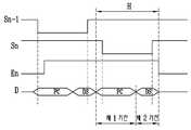
도 4는 도 3에 도시된 화소의 구동방법을 나타내는 파형도이다. 도 4에서 1 수평기간(1H)은 제 1기간 및 제 2기간으로 나누어 구동된다. 제 1기간 동안 데이터선들(D1 내지 Dm)에는 소정의 전류(PC : Predetermined Current)가 흐르고, 제 2기간 동안 데이터신호(DS)가 공급된다. 실제로, 제 1기간 동안에는 화소(140)로부터 데이터 구동회로(200)로 소정의 전류(PC)가 공급된다.(Current Sink) 그리고, 제 2기간 동안에는 데이터 구동회로(200)로부터 화소(140)로 데이터신호(DS)가 공급된다. 이후, 설명의 편의성을 위하여 기준전원(Vref)과 제 1전원(ELVDD)의 초기 전압값이 동일하게 설정된다고 가정하기로 한다.4 is a waveform diagram illustrating a method of driving the pixel illustrated in FIG. 3. In FIG. 4, one horizontal period 1H is driven by dividing into a first period and a second period. Predetermined current (PC) flows through the data lines D1 through Dm during the first period, and the data signal DS is supplied during the second period. In fact, a predetermined current PC is supplied from the
도 3 및 도 4를 결부하여 동작과정을 상세히 설명하면, 먼저 제 n-1주사선(Sn-1)으로 주사신호가 공급된다. 제 n-1주사선(Sn-1)으로 주사신호가 공급되면 제 3트랜지스터(M3) 및 제 5트랜지스터(M5)가 턴-온된다. 제 5트랜지스터(M5)가 턴-온되면 제 4트랜지스터(M4)가 다이오드 형태로 접속된다. 제 4트랜지스터(M4)가 다이오드 형태로 접속되면 제 2노드(N2)에는 제 1전원(ELVDD)에서 제 4트랜지스터(M4)의 문턱전압을 감한 전압값이 인가된다.3 and 4, the operation process is described in detail. First, a scan signal is supplied to the n−1 th scan line Sn−1. When the scan signal is supplied to the n-1 th scan line Sn-1, the third transistor M3 and the fifth transistor M5 are turned on. When the fifth transistor M5 is turned on, the fourth transistor M4 is connected in the form of a diode. When the fourth transistor M4 is connected in the form of a diode, a voltage value obtained by subtracting the threshold voltage of the fourth transistor M4 from the first power source ELVDD is applied to the second node N2.
그리고, 제 3트랜지스터(M3)가 턴-온되면 기준전원(Vref)의 전압이 제 1노드(N1)로 인가된다. 이때, 제 2커패시터(C2)는 제 1노드(N1)와 제 2노드(N2)의 차에 대응되는 전압을 충전한다. 이 경우, 기준전원(Vref)과 제 1전원(ELVDD)의 전압값이 동일하다고 가정하면 제 2커패시터(C2)에는 제 4트랜지스터(M4)의 문턱전압에 대응되는 전압이 충전된다. 그리고, 제 1전원(ELVDD)에서 소정의 전압강하가 발생된다면 제 2커패시터(C2)에는 제 4트랜지스터(M4)의 문턱전압 및 제 1전원(ELVDD)의 전압강하 전압이 충전된다. 즉, 본 발명에서는 제 n-1주사선(Sn-1)으로 주사신 호가 공급되는 기간 동안 제 1전원(ELVDD)의 전압강하 전압 및 제 4트랜지스터(M4)의 문턱전압이 제 2커패시터(C2)에 충전되고, 이에 따라 제 1전원(ELVDD)의 전압강하를 보상할 수 있다.When the third transistor M3 is turned on, the voltage of the reference power supply Vref is applied to the first node N1. In this case, the second capacitor C2 charges a voltage corresponding to the difference between the first node N1 and the second node N2. In this case, assuming that the voltage values of the reference power supply Vref and the first power supply ELVDD are the same, a voltage corresponding to the threshold voltage of the fourth transistor M4 is charged in the second capacitor C2. If a predetermined voltage drop occurs in the first power supply ELVDD, the threshold voltage of the fourth transistor M4 and the voltage drop voltage of the first power supply ELVDD are charged in the second capacitor C2. That is, in the present invention, the voltage drop voltage of the first power supply ELVDD and the threshold voltage of the fourth transistor M4 are equal to the second capacitor C2 during the period in which the scan signal is supplied to the n-1 scan line Sn-1. It is charged to the, thereby compensating for the voltage drop of the first power source (ELVDD).
제 2커패시터(C2)에 소정의 전압이 충전된 후 제 n주사선(Sn)으로 주사신호가 공급된다. 제 n주사선(Sn)으로 주사신호가 공급되면 제 1트랜지스터(M1) 및 제 2트랜지스터(M2)가 턴-온된다. 제 2트랜지스터(M2)가 턴-온되면 1수평기간의 제 1기간 동안 소정의 전류(PC)가 화소(140)로부터 데이터선(Dm)을 경유하여 데이터 구동회로(200)로 공급된다. 실제로, 소정의 전류(PC)는 제 1전원(ELVDD), 제 4트랜지스터(M4), 제 2트랜지스터(M2) 및 데이터선(Dm)을 경유하여 데이터 구동회로(200)로 공급된다. 이때, 제 1커패시터(C1) 및 제 2커패시터(C2)에는 소정의 전류(PC)에 대응하여 소정의 전압이 충전된다.After the predetermined voltage is charged in the second capacitor C2, the scan signal is supplied to the nth scan line Sn. When the scan signal is supplied to the nth scan line Sn, the first transistor M1 and the second transistor M2 are turned on. When the second transistor M2 is turned on, a predetermined current PC is supplied from the
한편, 데이터 구동회로(200)는 소정의 전류(PC)가 싱크될 때 발생되는 소정의 전압값(이후 "보상전압"이라 함)을 이용하여 감마 전압부(도시되지 않음)의 전압을 재설정하고, 재설정된 감마 전압부의 전압을 이용하여 데이터신호(DS)를 생성한다. 이후, 1수평기간의 제 2기간 동안 데이터신호(DS)가 제 1트랜지스터(M1)를 경유하여 제 1노드(N1)로 공급된다. 그러면, 제 1커패시터(C1)에는 데이터신호(DS)와 제 1전원(ELVDD1)의 차값에 대응하는 전압이 충전된다. 이때, 제 2노드(N2)는 플로팅상태로 설정되기 때문에 제 2커패시터(C2)는 이전에 충전된 전압을 유지한다.Meanwhile, the
즉, 본 발명에서는 이전 주사선으로 주사신호가 공급되는 기간 동안 제 2커 패시터(C2)에 제 4트랜지스터(M4)의 문턱전압 및 제 1전원(ELVDD)의 전압강하에 대응하는 전압을 충전함으로써 제 1전원(ELVDD)의 전압강하 및 제 4트랜지스터(M4)의 문턱전압을 보상할 수 있다. 그리고, 본 발명에서는 현재 주사선으로 주사신호가 공급되는 기간 동안 화소(140)에 포함된 트랜지스터들의 이동도 등이 보상되도록 감마 전압부의 전압을 재설정하고, 재설정된 감마 전압을 이용하여 생성된 데이터신호를 공급한다. 따라서, 본 발명에서는 트랜지스터의 문턱전압, 이동도 등의 불균일 등을 보상하여 균일한 화상을 표시할 수 있다. 감마 전압부의 전압이 재설정되는 과정등은 후술 하기로 한다.That is, in the present invention, the second capacitor C2 is charged with a voltage corresponding to the threshold voltage of the fourth transistor M4 and the voltage drop of the first power supply ELVDD during the period in which the scan signal is supplied to the previous scan line. The voltage drop of the first power supply ELVDD and the threshold voltage of the fourth transistor M4 may be compensated for. In the present invention, the voltage of the gamma voltage unit is reset to compensate for the mobility of the transistors included in the
도 5는 도 2에 도시된 화소의 다른례를 나타내는 도면이다. 도 5는 제 1커패시터(C1)가 제 2노드(N2)와 제 1전원(ELVDD) 사이에 설치되는 것을 제외하고는 도 3과 동일한 구성으로 설정된다.FIG. 5 is a diagram illustrating another example of the pixel illustrated in FIG. 2. FIG. 5 is set to the same configuration as FIG. 3 except that the first capacitor C1 is installed between the second node N2 and the first power source ELVDD.
도 4 및 도 5를 참조하여 동작과정을 상세히 설명하면, 먼저 제 n-1주사선(Sn-1)으로 주사신호가 공급된다. 제 n-1주사선(Sn-1)으로 주사신호가 공급되면 제 3트랜지스터(M3) 및 제 5트랜지터(M5)가 턴-온된다. 제 5트랜지스터(M5)가 턴-온되면 제 4트랜지스터(M4)가 다이오드 형태로 접속된다. 제 4트랜지스터(M4)가 다이오드 형태로 접속되면 제 2노드(N2)에는 제 1전원(ELVDD)에서 제 4트랜지스터(M4)의 문턱전압을 감한 전압값이 인가된다. 따라서, 제 1커패시터(C1)에는 제 4트랜지스터(M4)의 문턱전압에 대응되는 전압이 충전된다.4 and 5, the scan signal is first supplied to the n−1 th scan line Sn−1. When the scan signal is supplied to the n-1 th scan line Sn-1, the third transistor M3 and the fifth transistor M5 are turned on. When the fifth transistor M5 is turned on, the fourth transistor M4 is connected in the form of a diode. When the fourth transistor M4 is connected in the form of a diode, a voltage value obtained by subtracting the threshold voltage of the fourth transistor M4 from the first power source ELVDD is applied to the second node N2. Therefore, the first capacitor C1 is charged with a voltage corresponding to the threshold voltage of the fourth transistor M4.
그리고, 제 3트랜지스터(M3)가 턴-온되면 기준전원(Vref)의 전압이 제 1노드 (N1)로 인가된다. 그러면, 제 2커패시터(C2)는 제 1노드(N1)와 제 2노드(N2)의 차에 대응되는 전압이 충전된다. 여기서, 제 n-1주사선(Sn-1)으로 주사신호가 공급되는 기간 동안 제 1트랜지스터(M1) 및 제 2트랜지스터(M2)가 턴-오프되기 때문에 데이터신호(DS)는 화소(140)로 공급되지 않는다.When the third transistor M3 is turned on, the voltage of the reference power source Vref is applied to the first node N1. Then, the second capacitor C2 is charged with a voltage corresponding to the difference between the first node N1 and the second node N2. Here, since the first transistor M1 and the second transistor M2 are turned off during the period in which the scan signal is supplied to the n-1 th scan line Sn-1, the data signal DS is transferred to the
이후, 제 n주사선(Sn)으로 주사신호가 공급되어 제 1트랜지스터(M1) 및 제 2트랜지스터(M2)가 턴-온된다. 제 2트랜지스터(M2)가 턴-온되면 1수평기간의 제 1기간 동안 소정의 전류(PC)가 화소(140)로부터 데이터선(Dm)을 경유하여 데이터 구동회로(200)로 공급된다. 실제로, 소정의 전류(PC)는 제 1전원(ELVDD), 제 4트랜지스터(M4), 제 2트랜지스터(M2) 및 데이터선(Dm)을 경유하여 데이터 구동회로(200)로 공급된다. 이때, 제 1커패시터(C1) 및 제 2커패시터(C2)에는 소정의 전류(PC)에 대응하여 소정의 전압이 충전된다.Thereafter, the scan signal is supplied to the nth scan line Sn so that the first transistor M1 and the second transistor M2 are turned on. When the second transistor M2 is turned on, a predetermined current PC is supplied from the
한편, 데이터 구동회로(200)는 소정의 전류(PC)에 대응하여 인가되는 보상전압을 이용하여 감마 전압부의 전압을 재설정하고, 재설정된감마 전압부의 전압을 이용하여 데이터신호(DS)를 생성한다. 이후, 1수평기간의 제 2기간 동안 데이터신호(DS)가 제 1노드(N1)로 공급된다. 그러면, 제 1커패시터(C1) 및 제 2커패시터(C2)에는 데이터신호(DS)에 대응하여 소정의 전압이 충전된다.Meanwhile, the
실제로, 데이터신호(DS)가 공급되면 제 1노드(N1)의 전압이 기준전원(Vref)으로부터 데이터신호(DS)의 전압으로 하강된다. 이때, 제 2노드(N2)가 플로팅되어 있기 때문에 제 1노드(N1)의 전압 하강량에 대응되어 제 2노드(N2)의 전압값도 하강된다. 이 경우, 제 2노드(N2)에서 하강되는 전압값은 제 1커패시터(C1) 및 제 2 커패시터(C2)의 용량에 의해서 결정된다.In fact, when the data signal DS is supplied, the voltage of the first node N1 is lowered from the reference power supply Vref to the voltage of the data signal DS. At this time, since the second node N2 is floating, the voltage value of the second node N2 also decreases corresponding to the voltage drop amount of the first node N1. In this case, the voltage value dropped at the second node N2 is determined by the capacitances of the first capacitor C1 and the second capacitor C2.
제 2노드(N2)이 전압이 하강되면 제 1커패시터(C1)에는 제 2노드(N2)의 전압값에 대응하여 소정의 전압이 충전된다. 여기서, 기준전원(Vref)의 전압값은 고정되어 있기 때문에 제 1커패시터(C1)에 충전되는 전압은 데이터신호(DS)에 의하여 결정된다. 다시 말하여, 도 5에 도시된 화소(140)는 기준전원(Vref)과 데이터신호(DS)에 의하여 커패시터들(C1, C2)에 충전되는 전압값이 결정되기 때문에 제 1전원(ELVDD)의 전압강하에 무관하게 원하는 전압을 충전할 수 있다.When the voltage of the second node N2 drops, the first capacitor C1 is charged with a predetermined voltage corresponding to the voltage value of the second node N2. Here, since the voltage value of the reference power supply Vref is fixed, the voltage charged in the first capacitor C1 is determined by the data signal DS. In other words, in the
그리고, 본 발명에서는 화소(140)에 포함된 트랜지스터들의 이동도 등이 보상되도록 감마 전압부의 전압을 재설정하고, 재설정된 감마 전압을 이용하여 생성된 데이터신호를 공급한다. 따라서, 본 발명에서는 트랜지스터의 문턱전압, 이동도 등의 불균일 등을 보상하여 균일한 화상을 표시할 수 있다.In the present invention, the voltage of the gamma voltage unit is reset to compensate for the mobility of the transistors included in the
도 6은 도 2에 도시된 데이터 구동회로의 제 1실시예를 나타내는 블록도이다. 도 6에서는 설명의 편의성을 위하여 데이터 구동회로(200)가 j(j는 2이상의 자연수)개의 채널을 갖는다고 가정하기로 한다.FIG. 6 is a block diagram showing a first embodiment of the data driving circuit shown in FIG. In FIG. 6, it is assumed that the
도 6을 참조하면, 본 발명의 제 1실시예에 의한 데이터 구동회로(200)는 쉬프트 레지스터부(210), 샘플링 래치부(220), 홀딩 래치부(230), 감마 전압부(240), 디지털-아날로그 변환부(이하 "DAC부"라 함)(250), 제 1버퍼부(270), 제 2버퍼부(260), 전류 공급부(280) 및 선택부(290)를 구비한다.Referring to FIG. 6, the
쉬프트 레지스터부(210)는 타이밍 제어부(150)로부터 소스 쉬프트 클럭(SSC) 및 소스 스타트 펄스(SSP)를 공급받는다. 타이밍 제어부(150)로부터 소스 쉬프트 클럭(SSC) 및 소스 스타트 펄스(SSP)를 공급받은 쉬프트 레지스터부(210)는 소스 쉬프트 클럭(SSC)의 1주기 마다 소스 스타트 펄스(SSP)를 쉬프트 시키면서 순차적으로 j개의 샘플링 신호를 생성한다. 이를 위해, 쉬프트 레지스터부(210)는 j개의 쉬프트 레지스터(2101 내지 210j)를 구비한다.The
샘플링 래치부(220)는 쉬프트 레지스터부(210)로부터 순차적으로 공급되는 샘플링신호에 응답하여 데이터(Data)를 순차적으로 저장한다. 여기서, 샘플링 래치부(220)는 j개의 데이터(Data)를 저장하기 위하여 j개의 샘플링 래치(2201 내지 220j)를 구비한다. 그리고, 각각의 샘플링 래치들(2201 내지 220j)은 데이터(Data)의 비트수에 대응되는 크기를 갖는다. 예를 들어, 데이터(Data)들이 k비트로 구성되는 경우 샘플링 래치(2201 내지 220i) 각각은 k비트의 크기로 설정된다.The
홀딩 래치부(230)는 소스 출력 인에이블(SOE) 신호가 입력될 때 샘플링 래치부(220)로부터 데이터(Data)들을 입력받아 저장한다. 그리고, 홀딩 래치부(230)는 소스 출력 인에이블(SOE)가 입력될 때 자신에게 저장된 데이터(Data)들을 DAC부(250)로 공급한다. 여기서, 홀딩 래치부(230)는 j개의 데이터(Data)를 저장하기 위하여 j개의 홀딩 래치(2301 내지 230j)를 구비한다. 그리고, 각각의 홀딩 래치들(2301 내지 230j)은 데이터(Data)의 비트수에 대응되는 크기를 갖는다. 예를 들어, 홀딩 래치들(2301 내지 230j) 각각은 데이터(Data)들이 저장될 수 있도록 k비트로 설정된다.The holding
감마 전압부(240)는 k비트의 데이터(Data)에 대응하여 소정의 계조전압을 생 성하기 위한 j개의 전압 생성부(2401 내지 240j)를 구비한다. 각각의 전압 생성부(2401 내지 240j)는 도 8에 도시된 바와 같이 복수의 분압 저항들(R1 내지 Rl)로 구성되어 2k개의 계조전압을 생성한다. 여기서, 전압 생성부(2401 내지 240j) 각각은 제 2버퍼부(260)로부터 공급되는 보상전압을 이용하여 계조전압들의 전압값을 재설정하고, 재설정된 계조전압들을 DAC들(2501 내지 250j)로 공급한다.The
DAC부(250)는 데이터(Data)의 비트값에 대응하여 데이터신호(DS)를 생성하는 j개의 DAC(2501 내지 250j)를 구비한다. DAC(2501 내지 250j)들 각각은 홀딩 래치부(230)로부터 공급되는 데이터(Data)의 비트값에 대응하여 복수의 계조전압들 중 어느 하나를 선택하여 데이터신호(DS)를 생성한다.The
제 1버퍼부(270)는 DAC부(250)로부터 공급되는 데이터신호들(DS)을 선택부(290)로 공급한다. 이를 위하여, 제 1버퍼부(270)는 j개의 제 1버퍼(2701 내지 270j)를 구비한다.The
선택부(290)는 데이터선들(D1 내지 Dj)과 제 1버퍼들(2701 내지 270j)의 전기적 연결을 제어한다. 실제로, 선택부(290)는 1수평기간의 제 2기간 동안만 데이터선들(D1 내지 Dj)과 제 1버퍼들(2701 내지 270j)을 전기적으로 접속시키고, 그 외에는 데이터선들(D1 내지 Dj)과 제 1버퍼들(2701 내지 270j)을 접속시키지 않는다. 이를 위해, 선택부(290)는 j개의 스위칭부(2901 내지 290j)를 구비한다.The
전류 공급부(280)는 1수평기간의 제 1기간 동안 데이터선들(D1 내지 Dj)과 접속된 화소들(140)로부터 소정의 전류(PC)를 싱크한다. 실제로, 전류 공급부 (280)는 각각의 화소들(140)에서 흐를 수 있는 맥시멈 전류, 즉 화소(140)가 최대 휘도로 발광될 때 발광소자(OLED)로 공급되어야 할 전류를 싱크한다. 그리고, 전류 공급부(280)는 전류가 싱크될 때 발생되는 소정의 보상전압을 제 2버퍼부(260)로 공급한다. 이를 위해, 전류 공급부(280)는 j개의 전류 싱크부(2801 내지 280j)를 구비한다.The
제 2버퍼부(260)는 전류 공급부(280)로부터 공급되는 보상전압을 감마 전압부(240)로 공급한다. 이를 위해, 제 2버퍼부(260)는 j개의 제 2버퍼(2601 내지 260j)를 구비한다.The
한편, 본 발명의 데이터 구동회로(200)는 도 7과 같이 홀딩 래치부(230)의 다음단에 레벨 쉬프터부(300)를 더 포함할 수 있다.(제 2실시예) 레벨 쉬프터부(300)는 홀딩 래치부(230)로부터 공급되는 데이터(Data)의 전압레벨을 상승시켜 DAC부(250)로 공급한다. 외부 시스템으로부터 데이터 구동회로(200)로 높은 전압레벨을 가지는 데이터(Data)가 공급되면 전압레벨에 대응되어 높은 내압을 가지는 회로 부품들이 설치되어야 하기 때문에 제조비용이 증가된다. 따라서, 데이터 구동회로(200)의 외부에서는 낮은 전압레벨을 가지는 데이터(Data)를 공급하고, 이 낮은 전압레벨을 가지는 데이터(Data)를 레벨 쉬프터부(300)에서 높은 전압레벨로 승압시킨다.Meanwhile, the
도 8은 특정 채널에 설치되는 전압 생성부, DAC, 제 1버퍼, 제 2버퍼, 스위칭부, 전류 싱크부 및 화소의 연결관계를 나타내는 도면이다. 도 8에서는 설명의 편의성을 위하여 j번째 채널을 도시하며, 데이터선(Dj)이 도 3에 도시된 화소(140)와 접속된다고 가정하기로 한다.8 is a diagram illustrating a connection relationship between a voltage generator, a DAC, a first buffer, a second buffer, a switching unit, a current sinking unit, and a pixel installed in a specific channel. In FIG. 8, for convenience of description, the j th channel is illustrated, and it is assumed that the data line Dj is connected to the
도 8을 참조하면, 전압 생성부(240j)는 복수의 분압 저항들(R1 내지 Rl)을 구비한다. 분압 저항들(R1 내지 Rl)은 기준전원(Vref)과 제 2버퍼(260j) 사이에 위치되어 전압을 분압한다. 실제로, 분압 저항들(R1 내지 Rl)은 기준전원(Vref)과 제 2버퍼(260j)로부터 공급되는 보상전압 사이의 전압을 분압하여 복수의 계조전압(V0 내지 V2k-1)을 생성하고, 생성된 계조전압들(V0 내지 V2k-1)을 DAC(250j)로 공급한다.Referring to FIG. 8, the
DAC(250j)는 데이터(Data)의 비트값에 응답하여 계조전압들(V0 내지 V2k-1)들 중 어느 하나의 계조전압을 선택하고, 선택된 계조전압을 제 1버퍼(270j)로 공급한다. 여기서, DAC(250j)에서 선택된 계조전압은 데이터신호(DS)로 이용된다.The
제 1버퍼(270j)는 DAC(250j)로부터 공급되는 데이터신호(DS)를 스위칭부(290j)로 전달한다.The
스위칭부(290j)는 제 11트랜지스터(M11)를 구비한다. 이와 같은 제 11트랜지스터(M11)는 도 9에 도시된 제 1제어신호(CS1)에 의하여 제어된다. 즉, 제 11트랜지스터(M11)는 1수평기간(1H)의 제 2기간 동안 턴-온되고 제 1기간 동안 턴-오프된다. 따라서, 데이터신호(DS)는 1수평기간(1H) 중 제 2기간 동안 데이터선(Dj)으로 공급되고, 그 외의 기간 동안에는 공급되지 않는다.The
전류 싱크부(280j)는 제 2제어신호(CS2)에 의하여 제어되는 제 12트랜지스터 (M12) 및 제 13트랜지스터(M13)와, 제 13트랜지스터(M13)의 제 1전극에 접속되는 전류원(Imax)과, 제 3노드(N3)와 기저전압원(GND) 사이에 접속되는 제 3커패시터(C3)를 구비한다.The
제 12트랜지스터(M12)의 게이트전극은 제 13트랜지스터(M13)의 게이트전극에 접속되고, 제 2전극은 제 13트랜지스터(M13)의 제 2전극과 데이터선(Dj)에 접속된다. 그리고, 제 12트랜지스터(M12)의 제 1전극은 제 2버퍼(260j)에 접속된다. 이와 같은 제 12트랜지스터(M12)는 제 2제어신호(CS2)에 의하여 1수평기간(1H)의 제 1기간 동안 턴-온되고 제 2기간 동안 턴-오프된다.The gate electrode of the twelfth transistor M12 is connected to the gate electrode of the thirteenth transistor M13, and the second electrode is connected to the second electrode of the thirteenth transistor M13 and the data line Dj. The first electrode of the twelfth transistor M12 is connected to the
제 13트랜지스터(M13)의 게이트전극은 제 12트랜지스터(M12)의 게이트전극에 접속되고, 제 2전극은 데이터선(Dj)에 접속된다. 그리고, 제 13트랜지스터(M13)의 제 1전극은 전류원(Imax)에 접속된다. 이와 같은 제 13트랜지스터(M13)는 제 2제어신호(CS2)에 의하여 1수평기간(1H)의 제 1기간 동안 턴-온되고 제 2기간 동안 턴-오프된다.The gate electrode of the thirteenth transistor M13 is connected to the gate electrode of the twelfth transistor M12, and the second electrode is connected to the data line Dj. The first electrode of the thirteenth transistor M13 is connected to the current source Imax. The thirteenth transistor M13 is turned on for the first period of the first horizontal period 1H and turned off for the second period by the second control signal CS2.
전류원(Imax)은 화소(140)가 최대 휘도로 발광될 때 발광소자(OLED)로 공급되어야 할 전류를 제 12트랜지스터(M12) 및 제 13트랜지스터(M13)가 턴-온되는 제 1기간 동안 화소(140)로부터 공급받는다.The current source Imax is a pixel for a first period during which the twelfth transistor M12 and the thirteenth transistor M13 are turned on for the current to be supplied to the light emitting device OLED when the
제 3커패시터(C3)는 전류원(Imax)에 의하여 화소(140)로부터 전류가 싱크될 때 제 3노드(N3)에 인가되는 보상전압을 저장한다. 실제로, 제 3커패시터(C3)는 제 1기간 동안 제 3노드(N3)에 인가되는 보상전압을 충전하고, 제 12트랜지스터(M13) 및 제 13트랜지스터(M13)가 턴-오프되더라도 제 3노드(N3)의 보상전압을 일 정하게 유지한다.The third capacitor C3 stores a compensation voltage applied to the third node N3 when the current is sinked from the
제 2버퍼(260j)는 제 3노드(N3)에 인가되는 보상전압, 즉 제 3커패시터(C3)에 충전된 전압을 전압 생성부(240j)로 공급한다. 그러면, 전압 생성부(240j)는 기준전원(Vref)과 제 2버퍼(260j)로부터 공급되는 보상전압 사이의 전압을 분압하게 된다. 여기서, 제 3노드(N3)에 인가되는 보상전압은 화소(140)에 포함된 트랜지스터들의 이동도 등에 의하여 화소(140)마다 동일 또는 상이하게 설정된다. 실제로, j개의 전압 생성부(2401 내지 240j)로 각각 공급되는 보상전압은 현재 접속된 화소(140)에 의하여 결정된다.The
한편, j개의 전압 생성부(2401 내지 240j)로 서로 다른 보상전압이 공급된다면 j개의 채널마다 설치되는 DAC(2501 내지 250j)로 공급되는 계조전압들(V0 내지 V2k-1)의 전압값도 상이하게 설정된다. 여기서, 계조전압들(V0 내지 V2k-1)은 각각의 데이터선(D1 내지 Dj)들이 현재 접속된 화소(140)에 의하여 제어되기 때문에 화소(140)에 포함된 트랜지스터들의 이동도 등이 불균일하더라도 화소부(130)에서는 균일한 화상을 표시할 수 있다.Meanwhile, if different compensation voltages are supplied to the
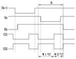
도 9는 도 8에 도시된 스위칭부, 전류 싱크부 및 화소로 공급되는 구동파형을 나타내는 도면이다.FIG. 9 is a diagram illustrating driving waveforms supplied to the switching unit, the current sink unit, and the pixel illustrated in FIG. 8.
도 8 및 도 9를 결부하여 화소(140)로 공급되는 데이터신호(DS)의 전압값을 상세히 설명하기로 한다. 먼저 제 n-1주사선(Sn-1)으로 주사신호가 공급된다. 제 n-1주사선(Sn-1)으로 주사신호가 공급되면 제 3트랜지스터(M3) 및 제 5트랜지스터(M5)가 턴-온된다. 그러면, 제 2노드(N2)에는 제 1전원(ELVDD)에서 제 4트랜지스터(M4)의 문턱전압을 감한 전압값이 인가되고, 제 1노드(N1)에는 기준전원(Vref)의 전압이 인가된다. 이때, 제 2커패시터(C2)에는 제 1전원(ELVDD)의 전압강하 전압 및 제 4트랜지스터(M4)의 문턱전압에 대응되는 전압이 충전된다.The voltage value of the data signal DS supplied to the
실제로, 제 1노드(N1) 및 제 2노드(N2) 각각에 인가되는 전압은 수학식 1과 같이 표현될 수 있다.In fact, the voltage applied to each of the first node N1 and the second node N2 may be expressed by

수학식 1에서 VN1은 제 1노드(N1)에 인가되는 전압, VN2는 제 2노드(N2)에 인가되는 전압, VthM4는 제 4트랜지스터(M4)의 문턱전압을 나타낸다.In
한편, 제 n-1주사선(Sn-1)으로 공급되는 주사신호가 오프되는 시점과 제 n주사선(Sn)으로 주사신호가 공급되는 시점 사이의 기간 동안 제 1노드(N1) 및 제 2노드(N2)는 플로팅 상태로 설정된다. 따라서, 제 2커패시터(C2)에 충전되는 전압값은 변화되지 않는다.On the other hand, during the period between the time when the scan signal supplied to the n-th scan line Sn-1 is turned off and the time when the scan signal is supplied to the nth scan line Sn, the first node N1 and the second node ( N2) is set to the floating state. Therefore, the voltage value charged in the second capacitor C2 is not changed.
이후, 제 n주사선(Sn)으로 주사신호가 공급되어 제 1트랜지스터(M1) 및 제 2트랜지스터(M2)가 턴-온된다. 그리고, 제 n주사선(Sn)으로 주사신호가 공급되는 기간 중 제 1기간 동안 제 12트랜지스터(M12) 및 제 13트랜지스터(M13)가 턴-온된다. 제 12트랜지스터(M12) 및 제 13트랜지스터(M13)가 턴-온되면 제 1전원 (ELVDD), 제 4트랜지스터(M4), 제 2트랜지스터(M2), 데이터선(Dj) 및 제 13트랜지스터(M13)를 경유하여 전류원(Imax)에 대응되는 전류가 싱크된다.Thereafter, the scan signal is supplied to the nth scan line Sn so that the first transistor M1 and the second transistor M2 are turned on. The twelfth transistor M12 and the thirteenth transistor M13 are turned on during the first period of the scan signal supplied to the nth scan line Sn. When the twelfth transistor M12 and the thirteenth transistor M13 are turned on, the first power source ELVDD, the fourth transistor M4, the second transistor M2, the data line Dj, and the thirteenth transistor M13 are turned on. The current corresponding to the current source Imax is sinked via).
이때, 제 4트랜지스터(M4)에는 전류원(Imax)의 전류가 흐르기 때문에 수학식 2와 같이 표현될 수 있다.At this time, since the current of the current source Imax flows in the fourth transistor M4, it may be expressed as

수학식 2에서 u는 이동도를 나타내고, Cox는 산화층의 용량, W는 채널 폭, L은 채널 길이를 나타낸다.In
수학식 2와 같은 전류가 제 4트랜지스터(M4)에 흐를 때 제 2노드(N2)에 인가되는 전압은 수학식 3과 같이 표현될 수 있다.When a current as shown in

그리고, 제 2커패시터(C2)의 커플링에 의하여 제 1노드(N1)에 인가되는 전압은 수학식 4와 같이 표현될 수 있다.The voltage applied to the first node N1 by the coupling of the second capacitor C2 may be expressed by Equation 4.

여기서, 제 1노드(N1)에 인가되는 전압(VN1)은 이상적으로 제 3노드(N3)에 인가되는 전압(VN3) 및 제 4노드(N4)에 인가되는 전압(VN4)과 동일하게 설정된다. 즉, 전류원(Imax)에 의하여 전류가 싱크될 때 제 4노드(N4)에는 수학식 4와 같은 전압이 인가된다.Here, the voltage VN1 applied to the first node N1 is ideally equal to the voltage VN3 applied to the third nodeN3 and the voltage VN4 applied to the fourth node N4. Is set to. That is, when the current is sinked by the current source Imax, the voltage as shown in Equation 4 is applied to the fourth node N4.
한편, 수학식 4에 도시된 바와 같이 제 3노드(N3) 및 제 4노드(N4)에 인가되는 전압은 현재 전류가 싱크되는 화소(140)에 포함된 트랜지스터의 이동도 등의 영향을 받게 된다. 따라서, 전류원(Imax)에 의하여 전류가 싱크될 때 제 3노드(N3) 및 제 4노드(N4)에 인가되는 전압값은 각각의 화소들(1409) 마다 상이하게 결정된다.(이동도가 상이한 경우)Meanwhile, as shown in Equation 4, the voltages applied to the third node N3 and the fourth node N4 are affected by the mobility of the transistor included in the
한편, 수학식 4에 의하여 구현된 전압이 제 4노드(N4)에 인가될 때 전압 생성부(240j)의 전압(Vdiff)은 수학식 5와 같이 표현될 수 있다.Meanwhile, when the voltage implemented by Equation 4 is applied to the fourth node N4, the voltage Vdiff of the

그리고, DAC(250j)에서 데이터(Data)에 대응하여 f(f는 자연수)개의 계조전압 중 h(h는 f 이하의 자연수)번째 계조전압을 선택하였다면 제 1버퍼(270j)로 공급되는 전압(Vb)은 수학식 6과 같이 표현될 수 있다.The voltage supplied to the

한편, 제 1기간 동안 전류가 싱크되어 제 3커패시터(C3)에 수학식 4와 같은 전압이 충전된 후 제 2기간 동안 제 12트랜지스터(M12) 및 제 13트랜지스터(M13)가 오프되고, 제 11트랜지스터(M11)가 턴-온된다. 이때, 제 3커패시터(C3)는 자신에게 충전된 전압값을 유지한다. 따라서, 제 3노드(N3)의 전압값은 수학식 4와 같이 유지될 수 있다.Meanwhile, after the current is sinked in the first period to charge the third capacitor C3 with the voltage as shown in Equation 4, the twelfth transistor M12 and the thirteenth transistor M13 are turned off for the second period, and the eleventh Transistor M11 is turned on. At this time, the third capacitor C3 maintains the voltage value charged thereto. Therefore, the voltage value of the third node N3 may be maintained as shown in Equation 4.
그리고, 제 2기간 동안 제 11트랜지스터(M11)가 턴-온되기 때문에 제 1버퍼(270j)로 공급된 전압은 제 11트랜지스터(M11), 데이터선(Dj) 및 제 1트랜지스터(M1)를 경유하여 제 1노드(N1)로 공급된다. 즉, 제 1노드(N1)로는 수학식 6과 같은 전압이 공급된다. 그리고, 제 2커패시터(C2)의 커플링에 의하여 제 2노드(N2)에 인가되는 전압은 수학식 7과 같이 표현될 수 있다.Since the eleventh transistor M11 is turned on during the second period, the voltage supplied to the

이때, 제 4트랜지스터(M4)를 경유하여 흐르는 전류는 수학식 8과 같이 나타낼 수 있다.In this case, the current flowing through the fourth transistor M4 may be represented by Equation (8).


수학식 8을 참조하면, 본 발명에서 제 4트랜지스터(M4)에서 흐르는 전류는 전압 생성부(240j)에서 생성된 계조전압에 의하여 결정된다. 즉, 본 발명에서는 제 4트랜지스터(M4)의 문턱전압, 이동도 등과 무관하게 계조전압에 의하여 결정되는 전류가 제 4트랜지스터(M4)로 흐를 수 있고, 이에 따라 균일한 화상을 표시할 수 있다.Referring to Equation 8, in the present invention, the current flowing in the fourth transistor M4 is determined by the gray voltage generated in the
한편, 본 발명에서 스위칭부(290j)의 구성은 다양하게 설정될 수 있다. 예를 들어, 스위칭부(290j)는 도 10과 같이 제 11트랜지스터(M11) 및 제 14트랜지스터(M14)가 트랜스미션 게이트(Transmission Gate) 형태로 접속될 수 있다. PMOS 타입으로 형성된 제 14트랜지스터(M14)는 제 2제어신호(CS2)를 공급받고, NMOS 타입으로 형성된 제 11트랜지스터(M11)는 제 1제어신호(CS1)를 공급받는다. 여기서, 제 1제어신호(CS1) 및 제 2제어신호(CS2)는 서로 반대의 극성을 갖기 때문에 제 11트랜지스터(M11) 및 제 14트랜지스터(M14)는 동일한 시간에 턴-온 및 턴-오프된다.Meanwhile, in the present invention, the configuration of the
한편, 제 11트랜지스터(M11) 및 제 14트랜지스터(M14)가 트랜스미션 게이트 (Transmission Gate) 형태로 접속되면 전압-전류 특성 곡선이 대략 직선 형태로 설정되기 때문에 스위칭에러를 최소화할 수 있다.On the other hand, when the 11th transistor M11 and the 14th transistor M14 are connected in the form of a transmission gate, the voltage-current characteristic curve is set in a substantially straight line shape, thereby minimizing switching errors.
도 11은 특정 채널에 설치되는 전압 생성부, DAC, 제 1버퍼, 제 2버퍼, 스위칭부, 전류 싱크부 및 화소의 연결관계를 나타내는 다른례이다. 도 11에서는 데이터선(Dj)에 접속된 화소(140)만 변경될 뿐 그 외의 구조는 도 8과 동일하게 설정된다. 따라서, 화소(140)로 공급되는 전압에 대해서만 간략히 설명하기로 한다.11 is another example illustrating a connection relationship between a voltage generator, a DAC, a first buffer, a second buffer, a switching unit, a current sinking unit, and a pixel installed in a specific channel. In FIG. 11, only the
도 9 및 도 11을 참조하면, 먼저 제 n-1주사선(Sn-1)으로 주사신호가 공급될 때 제 1노드(N1) 및 제 2노드(N2)에는 수학식 1에 기재된 전압이 인가된다.9 and 11, when the scan signal is first supplied to the n−1 th scan line Sn−1, the voltage described in
그리고, 제 n주사선(Sn)으로 주사신호가 공급되고, 제 12트랜지스터(M12) 및 제 13트랜지스터(M13)가 턴-온되는 제 1기간 동안 제 4트랜지스터(M4)에 흐르는 전류는 수학식 2와 같이 표현되고, 제 2노드(N2)에 인가되는 전압은 수학식 3과 같이 표현된다.The scan signal is supplied to the nth scan line Sn and the current flowing through the fourth transistor M4 during the first period during which the twelfth transistor M12 and the thirteenth transistor M13 is turned on is represented by
그리고, 제 2커패시터(C2)의 커플링에 의하여 제 1노드(N1)에 인가되는 전압은 수학식 9와 같이 표현될 수 있다.In addition, the voltage applied to the first node N1 by the coupling of the second capacitor C2 may be expressed as in Equation (9).

그리고, 제 1노드(N1)에 인가되는 전압은 제 3노드(N3) 및 제 4노드(N4)로 공급되기 때문에 전압 생성부(240j)의 전압(Vdiff)은 수학식 10과 같이 표현될 수 있다.In addition, since the voltage applied to the first node N1 is supplied to the third node N3 and the fourth node N4, the voltage Vdiff of the

그리고, DAC(250j)에서 f개의 계조전압 중 h번째 계조전압을 선택하였다면 제 1버퍼(270j)로 공급되는 전압(Vb)은 수학식 11과 같이 표현될 수 있다.If the h-th gray voltage is selected among the f gray voltages in the

제 1버퍼(270j)로 공급되는 전압은 제 1노드(N1)로 공급된다. 이때, 제 2노드(N2)에 인가되는 전압은 수학식 7과 같이 표현될 수 있다. 따라서, 제 4트랜지스터(M4)를 경유하여 흐르는 전류는 수학식 8과 같이 나타낼 수 있다. 즉, 본 발명에서 제 4트랜지스터(M4)를 경유하여 발광소자(OLED)로 공급되는 전류는 제 4트랜지스터(M4)의 문턱전압, 이동도 등과 무관하게 계조전압에 의하여 결정되기 때문에 균일한 화상을 표시할 수 있다.The voltage supplied to the
한편, 도 5에 도시된 바와 같은 화소(140)는 제 1노드(N1)의 전압이 크게 변하더라도 제 2노드(N2)의 전압이 둔감하게 변화된다.(즉, C1+C2/C2) 따라서, 도 5에 도시된 화소(140)가 적용되면 도 3에 도시된 화소(140)가 적용되는 경우보다 전 압 생성부(240j)의 전압 범위를 넓게 설정할 수 있다. 이와 같이, 전압 생성부(240j)의 전압 범위가 넓게 설정되면 제 11트랜지스터(M11) 및 제 1트랜지스터(M1) 등의 스위칭에러에 의한 영향을 줄일 수 있다는 장점이 있다.On the other hand, in the
한편, 상술한 도 8 및 도 11의 설명은 데이터선(Dj)의 부하를 고려하지 않은 이상적인 경우이다. 실제로, 소정의 전류(PC)가 싱크될 때 제 1노드(N1) 및 제 3노드(N3)에 인가되는 전압값은 데이터선(Dj)의 전압강하에 의하여 상이하게 설정된다. 즉, 소정의 전류(PC)가 싱크될 때 데이터선(Dj)의 전압강하에 의하여 제 3노드(N3)의 전압값은 제 1노드(N1)의 전압값보다 낮게 설정되고, 이에 따라 원하는 계조의 영상을 표시하지 못할 염려가 있다. 이와 같은 문제점을 극복하기 위하여 본 발명에서는 도 12와 같은 데이터 구동회로를 제안한다.8 and 11 are ideal cases without considering the load of the data line Dj. In fact, the voltage values applied to the first node N1 and the third node N3 when the predetermined current PC is sinked are set differently by the voltage drop of the data line Dj. That is, when the predetermined current PC is sinked, the voltage value of the third node N3 is set lower than the voltage value of the first node N1 due to the voltage drop of the data line Dj. You may not be able to display the video. In order to overcome such a problem, the present invention proposes a data driving circuit as shown in FIG.
도 12는 도 2에 도시된 데이터 구동회로의 제 3실시예를 나타내는 블록도이다. 도 12에서 도 6과 동일한 구성은 동일한 도면부호를 할당함과 아울러 상세한 설명은 생략하기로 한다.FIG. 12 is a block diagram showing a third embodiment of the data driving circuit shown in FIG. In FIG. 12, the same components as those in FIG. 6 are assigned the same reference numerals and detailed description thereof will be omitted.
도 12을 참조하면, 본 발명의 제 3실시예에 의한 데이터 구동회로(200)는 쉬프트 레지스터부(210), 샘플링 래치부(220), 홀딩 래치부(230), DAC부(250), 제 1버퍼부(270), 제 2버퍼부(260), 전류 공급부(280), 선택부(290), 감마 전압부(400) 및 승압블록(410)을 구비한다.Referring to FIG. 12, the
감마 전압부(400)는 k비트의 데이터(Data)에 대응하여 소정의 계조전압을 생성하기 위한 j개의 전압 생성부(4001 내지 400j)를 구비한다. 각각의 전압 생성부 (4001 내지 400j)는 도 14에 도시된 바와 같이 복수의 분압 저항들(R1 내지 Rl)로 구성되어 2k개의 계조전압을 생성한다. 실제로, 분압 저항들(R1 내지 Rl)은 제 2기준전원(Vref2)과 제 2버퍼부(260)로부터 공급되는 보상전압을 분압하여 계조전압들을 생성하고, 생성된 계조전압들을 DAC들(2501 내지 250j)로 공급한다. 여기서, 제 2기준전원(Vref2)은 기준전원(Vref) 전압값에서 전류 공급부(280)에서 전류를 싱크할 때 발생되는 전압강하 전압(ΔV)을 감한 값으로 설정된다.(즉, Vref2 = Vref - ΔV)The
승압블록(410)은 DAC부(250)와 제 1버퍼부(270) 사이에 설치되는 j개의 승압부(4101 내지 410j)를 구비한다. 승압부(4101 내지 410j) 각각은 DAC들(2501 내지 250j) 각각으로부터 계조전압을 공급받는다. 계조전압을 공급받은 승압부(4101 내지 410j) 각각은 기준전원(Vref)과 제 2기준전원(Vref2)의 차에 대응하되는 전압(ΔV)을 승압한다. 즉, 승압부(4101 내지 410j) 각각은 화소들(140)에서 원하는 화상이 표시되도록 계조전압의 전압을 데이터선의 전압강하 전압(ΔV) 만큼 승압시킨다.The boosting
한편, 본 발명의 데이터 구동회로(200)는 도 13과 같이 홀딩 래치부(230)의 다음단에 레벨 쉬프터부(300)를 더 포함할 수 있다.(제 4실시예) 레벨 쉬프터부(300)는 홀딩 래치부(230)로부터 공급되는 데이터(Data)의 전압레벨을 상승시켜 DAC부(250)로 공급한다. 외부 시스템으로부터 데이터 구동회로(200)로 높은 전압레벨을 가지는 데이터(Data)가 공급되면 전압레벨에 대응되어 높은 내압을 가지는 회로 부품들이 설치되어야 하기 때문에 제조비용이 증가된다. 따라서, 데이터 구동회로(200)의 외부에서는 낮은 전압레벨을 가지는 데이터(Data)를 공급하고, 이 낮은 전압레벨을 가지는 데이터(Data)를 레벨 쉬프터부(300)에서 높은 전압레벨로 승압시킨다.Meanwhile, the
도 14는 특정 채널에 설치되는 전압 생성부, DAC, 승압부, 제 1버퍼, 제 2버퍼, 스위칭부, 전류 싱크부 및 화소의 연결관계를 나타내는 도면이다. 도 14에서는 설명의 편의성을 위하여 j번째 채널을 도시하며, 데이터선(Dj)이 도 3에 도시된 화소(140)와 접속된다고 가정하기로 한다. 여기서, 데이터선(Dj)에 도 5에 도시된 화소(140)가 접속되어도 승압부(410j) 및 전압 생성부(400j)의 동작과정은 동일하므로 도 5의 화소(140)가 접속되었을 때의 동작과정은 생략하기로 한다.FIG. 14 is a diagram illustrating a connection relationship between a voltage generator, a DAC, a booster, a first buffer, a second buffer, a switching unit, a current sinker, and a pixel installed in a specific channel. In FIG. 14, for convenience of description, the j th channel is illustrated, and it is assumed that the data line Dj is connected to the
도 14를 참조하면, 전압 생성부(400j)는 복수의 분압 저항들(R1 내지 Rl)을 구비한다. 분압 저항들(R1 내지 Rl)은 제 2기준전원(Vref2)과 제 2버퍼(260j) 사이에 위치되어 전압을 분압한다. 실제로, 분압 저항들(R1 내지 Rl)은 제 2기준전원(Vref2)과 제 2버퍼(260j)로부터 공급되는 보상전압 사이의 전압을 분압하여 복수의 계조전압(V0 내지 V2k-1)을 생성하고, 생성된 계조전압들(V0 내지 V2k-1)을 DAC(250j)로 공급한다.Referring to FIG. 14, the
여기서, 제 2기준전원(Vref2)의 전압값은 현재 접속된 화소(140)의 위치에 따라서 상이하게 설정된다. 실제로, 제 1주사선(S1)과 접속된 화소(140)에서 발생 되는 전압강하 전압(ΔV)과 제 n주사선(Sn)과 접속된 화소(140)에서 발생되는 전압강하 전압(ΔV)은 상이하게 설정된다. 제 2기준전원(Vref2)의 전압은 화소들(140)에서 발생되는 전압강하 전압(ΔV)을 고려하여 다양한 방법으로 구해질 수 있다. 예를 들어, 도시되지 않은 메모리에 미리 각각의 화소(140)들의 전압강하 전압(ΔV)을 저장하고, 이 저장된 전압에 대응하는 제 2기준전원(Vre2)을 전압 생성부(400j) 및 승압부(410j)로 제공할 수 있다. 실제로, 제 2기준전원(Vref2)의 전압을 생성하기 위한 방법은 본원 출원인에 의하여 본원과 동일날짜로 출원되었다.Here, the voltage value of the second reference power supply Vref2 is set differently according to the position of the
DAC(250j)는 데이터(Data)의 비트값에 응답하여 계조전압들(V0 내지 V2k-1)들 중 어느 하나의 계조전압을 선택하고, 선택된 계조전압을 제 1버퍼(270j)로 공급한다. 여기서, DAC(250j)에서 선택된 계조전압은 데이터신호(DS)로 이용된다.The
승압부(410j)는 기준전원(Vref)의 전압에서 제 2기준전원(Vref2)의 전압값을 감하여 전압강하 전압(ΔV)을 생성하고, 전압강하 전압(ΔV) 만큼 데이터신호(DS)의 전압을 승압시킨다. 그러면, 화소부(140)에서는 원하는 휘도의 영상이 표시될 수 있다.The
도 9 및 도 14를 결부하여 전압 생성부(400j) 및 승압부(410j)의 동작과정을 상세히 설명하고, 나머지 구성들은 간략히 설명하기로 한다. 먼저, 제 n-1주사선(Sn-1)으로 주사신호가 공급될 때 제 1노드(N1) 및 제 2노드(N2)에 수학식 1과 같은 전압이 인가된다.The operation of the
이후, 제 n주사선(Sn)으로 주사신호가 공급되는 기간 중 제 1기간 동안 전류 원(Imax)에 의하여 싱크되는 전류값에 대응하여 제 1노드(N1)에 수학식 4와 같은 전압값이 인가된다. 그리고, 데이터선(Dj)의 부하에 의하여 제 3노드(N3)에는 수학식 12와 같은 전압이 인가된다.Subsequently, a voltage value as shown in Equation 4 is applied to the first node N1 in response to the current value sinked by the current source Imax during the first period of time during which the scan signal is supplied to the nth scan line Sn. do. Then, a voltage as shown in Equation 12 is applied to the third node N3 by the load of the data line Dj.

즉, 제 3노드(N3)에는 제 1노드(N1)에 인가된 전압값에서 데이터선(Dj)에 의한 전압강하 전압(ΔV)을 감한 전압값이 인간된다. 그리고, 제 3노드(N3)의 전압값은 제 2버퍼(260j)를 경유하여 제 4노드(N4)로 공급되기 때문에 제 3노드(N3)의 전압과 제 4노드(N4)의 전압은 동일하게 설정된다.That is, the voltage value obtained by subtracting the voltage drop voltage? V by the data line Dj from the voltage value applied to the first node N1 is human. Since the voltage value of the third node N3 is supplied to the fourth node N4 via the
그러면, 전압 생성부(400j)는 제 4노드(N4)에 인가되는 보상전압과 제 2기준전원(Vref2)의 전압을 분압하여 다수의 계조전압(V0 내지 V2k-1)을 생성하고, 생성된 계조전압(V0 내지 V2k-1)을 DAC(250j)로 공급한다. DAC(250j)는 데이터(Data)의 비트값에 대응하여 f(f는 자연수)개의 계조전압 중 h(h는 f 이하의 자연수)번째 계조전압을 데이터신호(DS)로 선택한다.Then, the
승압부(410j)는 DAC(250j)로부터 공급되는 데이터신호(DS)의 전압을 전압강하 전압(ΔV) 만큼 상승시킨다. 실제로, 승압부(410j)는 기준전원(Vref)에서 제 2기준전원(Vref2)의 전압값을 감하여 전압강하 전압(ΔV)을 생성하고, 생성된 전압강하 전압(ΔV) 만큼 데이터신호(DS)의 전압을 승압한다. 그러면, 제 1버퍼(270j) 로는 수학식 6과 같은 전압이 공급된다. 한편, 승압부(410j)는 도 15와 같이 외부로부터 전압강하 전압(ΔV)을 공급받고, 공급된 전압강하 전압(ΔV) 만큼 데이터신호(DS)의 전압을 승압할 수 도 있다.The
이후, 수평기간의 제 2기간 동안 제 11트랜지스터(M11)가 턴-온되어 제 1버퍼(270j)로 공급된 전압이 제 1노드(N1)로 공급된다. 그러면, 제 1노드(N1)에는 수학식 6과 같은 전압이 공급되고, 제 2노드(N2)에는 수학식 7과 같은 전압이 인가된다. 이때, 제 4트랜지스터(M4)에는 수학식 8과 같은 전류가 흐르게 된다. 즉, 본 발명의 제 3실시예에 의한 데이터 구동회로(200)에서는 전류가 싱크될 때 데이터선(Dj)에 의하여 발생되는 전압강하 전압(ΔV)을 보상하는 과정만 추가될 뿐 나머지 동작과정을 본 발명의 제 1실시예에 의한 데이터 구동회로(200)와 동일하다.Thereafter, the eleventh transistor M11 is turned on during the second period of the horizontal period, and the voltage supplied to the
도 16은 도 2에 도시된 데이터 구동회로의 제 5실시예를 나타내는 블록도이다. 도 16에서 도 6과 동일한 구성은 동일한 도면부호를 할당함과 아울러 상세한 설명은 생략하기로 한다.FIG. 16 is a block diagram showing a fifth embodiment of the data driving circuit shown in FIG. In FIG. 16, the same components as those in FIG. 6 are assigned the same reference numerals and detailed description thereof will be omitted.
도 16을 참조하면, 본 발명의 제 5실시예에 의한 데이터 구동회로(200)는 쉬프트 레지스터부(210), 샘플링 래치부(220), 홀딩 래치부(230), 감마 전압부(240), DAC부(250), 제 1버퍼부(270), 제 2버퍼부(260), 전류 공급부(280), 선택부(290) 및 승압블록(420)을 구비한다.Referring to FIG. 16, the
승압블록(420)은 전류 공급부(280)와 접속되도록 위치된다. 이와 같은 승압블록(420)은 j개의 승압부(4201 내지 420j)를 구비한다. 승압부(4201 내지 420j) 각각은 전류 싱크부들(2801 내지 280j) 중 어느 하나와 접속되어 전류 싱크부(2801 내지 280j)에서 생성되는 보상전압의 전압값을 승압시킨다. 실제로, 승압부(4201 내지 420j) 각각은 기준전원(Vref)과 제 2기준전원(Vref2)을 공급받고, 기준전원(Vref)과 제 2기준전원(Vref2)의 차에 대응하되는 전압(ΔV)을 승압한다. 즉, 승압부(4201 내지 420j) 각각은 데이터선의 부하에 발생되는 전압강하 전압(ΔV) 만큼 보상전압을 승압시킨다.The
감마 전압부(240)는 k비트의 데이터(Data)에 대응하여 소정의 계조전압을 생성하기 위한 j개의 전압 생성부(2401 내지 240j)를 구비한다. 각각의 전압 생성부(2401 내지 240j)는 도 17에 도시된 바와 같이 복수의 분압 저항들(R1 내지 Rl)로 구성되어 2k개의 계조전압을 생성한다. 실제로, 분압 저항들(R1 내지 Rl)은 기준전원(Vref)과 제 2버퍼부(260)로부터 공급되는 보상전압을 분압하여 계조전압들을 생성하고, 생성된 계조전압들을 DAC들(2501 내지 250j)로 공급한다. 즉, 감마 전압부(240)는 승압블록(420)에 의하여 승압된 보상전압을 공급받기 때문에 기준전원(Vref)과 보상전압 사이의 전압을 분압한다. 한편, 본 발명의 데이터 구동회로(200)는 홀딩 래치부(230)의 다음단에 도 13과 같은 레벨 쉬프터부(300)를 더 포함할 수 있다.The
도 17은 특정 채널에 설치되는 전압 생성부, DAC, 제 1버퍼, 제 2버퍼, 스위칭부, 전류 싱크부, 승압부 및 화소의 연결관계를 나타내는 도면이다. 도 17에서 는 설명의 편의성을 위하여 j번째 채널을 도시하며, 데이터선(Dj)이 도 3에 도시된 화소(140)와 접속된다고 가정하기로 한다. 여기서, 데이터선(Dj)에 도 5에 도시된 화소(140)가 접속되어도 승압부(420j)의 동작과정은 동일하므로 도 5의 화소(140)가 접속되었을 때의 동작과정은 생략하기로 한다.17 is a diagram illustrating a connection relationship between a voltage generator, a DAC, a first buffer, a second buffer, a switching unit, a current sinking unit, a boosting unit, and a pixel installed in a specific channel. In FIG. 17, for convenience of description, the j th channel is illustrated, and it is assumed that the data line Dj is connected to the
도 17을 참조하면, 승압부(420j)는 제 3커패시터(C3)의 일측단자에 접속된다. 이와 같은 승압부(420j)는 제 3버퍼(421)와, 제 15트랜지스터(M15) 및 제 16트랜지스터(M16)를 구비한다.Referring to FIG. 17, the boosting
제 15트랜지스터(M15)의 제 1전극은 제 2기준전원(Vref2)에 접속되고, 제 2전극은 제 3버퍼(421)에 접속된다. 그리고, 제 15트랜지스터(M15)의 게이트전극은 제 2제어신호(CS2)를 공급받는다. 이와 같은 제 15트랜지스터(M15)는 수평기간(H)의 제 1기간 동안 턴-온되고, 제 2기간 동안 턴-오프된다.The first electrode of the fifteenth transistor M15 is connected to the second reference power supply Vref2, and the second electrode is connected to the
제 16트랜지스터(M16)의 제 1전극은 기준전원(Vref)에 접속되고, 제 2전극은 제 3버퍼(421)에 접속된다. 그리고, 제 16트랜지스터(M16)의 게이트전극은 제 1제어신호(CS1)를 공급받는다. 이와 같은 제 16트랜지스터(M16)는 수평기간(H)의 제 2기간 동안 턴-온되고, 제 1기간 동안 턴-오프된다.The first electrode of the sixteenth transistor M16 is connected to the reference power supply Vref, and the second electrode is connected to the
제 3버퍼(421)는 제 15트랜지스터(M15) 또는 제 16트랜지스터(M16)로부터 공급되는 제 2기준전원(Vref2) 또는 제 1기준전원(Vref)의 전압을 제 3커패시터(C3)의 일측단자로 공급한다.The
도 9 및 도 17을 결부하여 승압부(420j)의 동작과정을 상세히 설명하기로 한다. 먼저, 제 n-1주사선(Sn-1)으로 주사신호가 공급될 때 제 1노드(N1) 및 제 2노 드(N2)에 수학식 1과 같은 전압이 인가된다.9 and 17, the operation of the
이후, 제 n주사선(Sn)으로 주사신호가 공급되는 기간 중 제 1기간 동안 전류원(Imax)에 의하여 싱크되는 전류값에 대응하여 제 1노드(N1)에 수학식 4와 같은 전압값이 인가된다. 그리고, 데이터선(Dj)의 부하에 의하여 제 3노드(N3)에는 수학식 12와 같은 전압이 인가된다. 즉, 제 3노드(N3)에는 제 1노드(N1)에 인가된 전압값에서 데이터선(Dj)에 의한 전압강하 전압(ΔV)을 감한 전압값이 인간된다. 한편, 제 1기간 동안 제 15트랜지스터(M15)가 턴-온되어 제 3커패시터(C3)의 일측단자로 제 2기준전원(Vref2)의 전압이 인가된다.Subsequently, a voltage value as shown in Equation 4 is applied to the first node N1 in response to the current value sinked by the current source Imax during the first period of time during which the scan signal is supplied to the nth scan line Sn. . Then, a voltage as shown in Equation 12 is applied to the third node N3 by the load of the data line Dj. That is, the voltage value obtained by subtracting the voltage drop voltage? V by the data line Dj from the voltage value applied to the first node N1 is human. Meanwhile, during the first period, the fifteenth transistor M15 is turned on so that the voltage of the second reference power supply Vref2 is applied to one terminal of the third capacitor C3.
제 3노드(N3)에 수학식 12와 같은 전압이 인가된 후 제 2기간 동안 제 15트랜지스터(M15)가 턴-오프되고, 제 16트랜지스터(M16)가 턴-온된다. 제 16트랜지스터(M16)가 턴-온되면 제 3커패시터(C3)의 일측단자로 기준전원(Vref)의 전압이 인가된다. 여기서, 기준전원(Vref)의 전압에서 제 2기준전원(Vref2)을 감한 전압값은 데이터선(Dj)의 전압강하 전압(ΔV)으로 설정되기 때문에 제 3노드(N3)의 전압값은 전압강하 전압(ΔV) 만큼 상승된다. 즉, 제 16트랜지스터(M16)가 턴-온되면 제 3노드(N3) 및 제 4노드(N4)에는 수학식 4와 같은 전압이 인가된다.After the voltage as shown in Equation 12 is applied to the third node N3, the fifteenth transistor M15 is turned off for the second period, and the sixteenth transistor M16 is turned on. When the sixteenth transistor M16 is turned on, the voltage of the reference power source Vref is applied to one terminal of the third capacitor C3. Here, since the voltage value obtained by subtracting the second reference power supply Vref2 from the voltage of the reference power supply Vref is set to the voltage drop voltage ΔV of the data line Dj, the voltage value of the third node N3 is the voltage drop. It rises by the voltage (DELTA) V. That is, when the sixteenth transistor M16 is turned on, a voltage as shown in Equation 4 is applied to the third node N3 and the fourth node N4.
이후, 전압 생성부(240j)는 제 4노드(N4)에 인가되는 보상전압과 기준전원(Vref)의 전압을 분압하여 다수의 계조전압(V0 내지 V2k-1)을 생성하고, 생성된 계조전압(V0 내지 V2k-1)을 DAC(250j)로 공급한다. DAC(250j)는 데이터(Data)의 비트값에 대응하여 f(f는 자연수)개의 계조전압 중 h(h는 f 이하의 자연수)번째 계조 전압을 데이터신호(DS)로 선택한다. 그러면, 제 1버퍼(270j)로는 수학식 6과 같은 전압이 공급된다.Thereafter, the
한편, 제 2기간 동안 제 11트랜지스터(M11)가 턴-온되기 때문에 제 1버퍼(270j)로 공급된 전압이 제 1노드(N1)로 공급된다. 그러면, 제 1노드(N1)에는 수학식 6과 같은 전압이 공급되고, 제 2노드(N2)에는 수학식 7과 같은 전압이 인가된다. 이때, 제 4트랜지스터(M4)에는 수학식 8과 같은 전류가 흐르게 된다. 즉, 본 발명의 제 3실시예에 의한 데이터 구동회로(200)에서는 전류가 싱크될 때 데이터선(Dj)에 의하여 발생되는 전압강하 전압(ΔV)을 보상하는 과정만 추가될 뿐 나머지 동작과정을 본 발명의 제 1실시예에 의한 데이터 구동회로(200)와 동일하다.Meanwhile, since the eleventh transistor M11 is turned on during the second period, the voltage supplied to the
상기 발명의 상세한 설명과 도면은 단지 본 발명의 예시적인 것으로서, 이는 단지 본 발명을 설명하기 위한 목적에서 사용된 것이지 의미 한정이나 특허청구범위에 기재된 본 발명의 범위를 제한하기 위하여 사용된 것은 아니다. 따라서, 이상 설명한 내용을 통해 당업자라면 본 발명의 기술사상을 일탈하지 아니하는 범위에서 다양한 변경 및 수정이 가능함을 알 수 있을 것이다. 따라서, 본 발명의 기술적 보호 범위는 명세서의 상세한 설명에 기재된 내용으로 한정되는 것이 아니라 특허청구범위에 의해 정하여 져야만 할 것이다.The above detailed description and drawings are merely exemplary of the present invention, but are used only for the purpose of illustrating the present invention and are not intended to limit the scope of the present invention as defined in the meaning or claims. Accordingly, those skilled in the art will appreciate that various changes and modifications can be made without departing from the technical spirit of the present invention. Therefore, the technical protection scope of the present invention should not be limited to the contents described in the detailed description of the specification but should be defined by the claims.
상술한 바와 같이, 본 발명의 실시 예에 따른 데이터 구동회로와 이를 이용한 발광 표시장치 및 그의 구동방법에 의하면 화소로부터 전류를 싱크할 때 발생되 는 보상전압을 이용하여 전압 생성부에서 생성되는 계조전압들의 전압값을 재설정하고, 재설정된 계조전압을 전류가 싱크된 화소로 공급하기 때문에 트랜지스터의 이동도와 무관하게 균일한 화상을 표시할 수 있다. 그리고, 본 발명에서는 데이터선에 의하여 발생되는 보상전압의 전압강하 전압을 보상하기 때문에 화소들에서 원하는 휘도의 영상을 표시할 수 있다.As described above, according to the data driving circuit, the light emitting display device using the same, and the driving method thereof, the gray scale voltages generated by the voltage generator are generated by using the compensation voltage generated when the current is sinked from the pixel. Since the voltage value is reset and the reset gradation voltage is supplied to the pixel in which the current is sinked, a uniform image can be displayed regardless of the mobility of the transistor. In the present invention, since the voltage drop voltage of the compensation voltage generated by the data line is compensated for, the pixels having the desired luminance can be displayed.
Claims (41)
Translated fromKoreanPriority Applications (5)
| Application Number | Priority Date | Filing Date | Title |
|---|---|---|---|
| KR1020050070433AKR100698699B1 (en) | 2005-08-01 | 2005-08-01 | Data driving circuit, light emitting display device and driving method thereof |
| CN200610057658ACN100583211C (en) | 2005-08-01 | 2006-02-22 | Data driving circuit and driving method of light emitting display using the same |
| JP2006080626AJP4612570B2 (en) | 2005-08-01 | 2006-03-23 | Data driving circuit, light emitting display device using the same, and driving method thereof |
| EP06251830.3AEP1758084B1 (en) | 2005-08-01 | 2006-03-31 | Data driving circuit and driving method of light emitting display using the same |
| US11/490,784US8217866B2 (en) | 2005-08-01 | 2006-07-20 | Data driving circuit and driving method of light emitting display using the same |
Applications Claiming Priority (1)
| Application Number | Priority Date | Filing Date | Title |
|---|---|---|---|
| KR1020050070433AKR100698699B1 (en) | 2005-08-01 | 2005-08-01 | Data driving circuit, light emitting display device and driving method thereof |
Publications (2)
| Publication Number | Publication Date |
|---|---|
| KR20070015822A KR20070015822A (en) | 2007-02-06 |
| KR100698699B1true KR100698699B1 (en) | 2007-03-23 |
Family
ID=37056885
Family Applications (1)
| Application Number | Title | Priority Date | Filing Date |
|---|---|---|---|
| KR1020050070433AExpired - LifetimeKR100698699B1 (en) | 2005-08-01 | 2005-08-01 | Data driving circuit, light emitting display device and driving method thereof |
Country Status (5)
| Country | Link |
|---|---|
| US (1) | US8217866B2 (en) |
| EP (1) | EP1758084B1 (en) |
| JP (1) | JP4612570B2 (en) |
| KR (1) | KR100698699B1 (en) |
| CN (1) | CN100583211C (en) |
Families Citing this family (44)
| Publication number | Priority date | Publication date | Assignee | Title |
|---|---|---|---|---|
| US8659511B2 (en) | 2005-08-10 | 2014-02-25 | Samsung Display Co., Ltd. | Data driver, organic light emitting display device using the same, and method of driving the organic light emitting display device |
| KR100658265B1 (en)* | 2005-08-10 | 2006-12-14 | 삼성에스디아이 주식회사 | Data driving circuit, light emitting display device and driving method thereof |
| JP2008107785A (en)* | 2006-09-29 | 2008-05-08 | Seiko Epson Corp | Electro-optical device and electronic apparatus |
| KR100865396B1 (en) | 2007-03-02 | 2008-10-24 | 삼성에스디아이 주식회사 | Organic electroluminescent display |
| KR100889680B1 (en) | 2007-07-27 | 2009-03-19 | 삼성모바일디스플레이주식회사 | Organic light emitting display device and driving method thereof |
| KR101361275B1 (en)* | 2007-08-08 | 2014-02-11 | 엘지전자 주식회사 | Digital-analog converter of digital display device |
| KR100893482B1 (en) | 2007-08-23 | 2009-04-17 | 삼성모바일디스플레이주식회사 | Organic light emitting display device and driving method thereof |
| KR100902594B1 (en)* | 2007-08-29 | 2009-06-11 | 주식회사 동부하이텍 | Display driver and its driving method |
| KR100894606B1 (en)* | 2007-10-29 | 2009-04-24 | 삼성모바일디스플레이주식회사 | Organic electroluminescent display and power supply method thereof |
| KR100902238B1 (en)* | 2008-01-18 | 2009-06-11 | 삼성모바일디스플레이주식회사 | Organic light emitting display device and driving method thereof |
| KR100969770B1 (en) | 2008-07-17 | 2010-07-13 | 삼성모바일디스플레이주식회사 | Organic light emitting display device and driving method thereof |
| JP5540556B2 (en)* | 2009-04-28 | 2014-07-02 | カシオ計算機株式会社 | Display device and driving method thereof |
| KR101056293B1 (en)* | 2009-10-26 | 2011-08-11 | 삼성모바일디스플레이주식회사 | Pixel and organic light emitting display device using same |
| KR101101097B1 (en)* | 2009-11-04 | 2012-01-03 | 삼성모바일디스플레이주식회사 | Organic light emitting display device and driving method thereof |
| TWI397887B (en)* | 2009-12-31 | 2013-06-01 | Au Optronics Corp | Driving device of light emitting unit |
| JP2011145481A (en)* | 2010-01-14 | 2011-07-28 | Sony Corp | Display device, and display driving method |
| CN101778509B (en)* | 2010-01-20 | 2012-11-07 | 友达光电股份有限公司 | Driving device of luminous element |
| CN102385834A (en)* | 2010-09-01 | 2012-03-21 | 华凌光电(常熟)有限公司 | Structure for adjusting organic light-emitting diode display with standing current and driving method thereof |
| US8513897B2 (en)* | 2010-10-01 | 2013-08-20 | Winstar Display Co., Ltd | OLED display with a current stabilizing device and its driving method |
| KR101738920B1 (en)* | 2010-10-28 | 2017-05-24 | 삼성디스플레이 주식회사 | Organic Light Emitting Display Device |
| JP2013061390A (en)* | 2011-09-12 | 2013-04-04 | Canon Inc | Display device |
| CN103106866B (en)* | 2011-11-15 | 2016-03-02 | 群康科技(深圳)有限公司 | Display device |
| KR101893167B1 (en) | 2012-03-23 | 2018-10-05 | 삼성디스플레이 주식회사 | Pixel circuit, method of driving the same, and method of driving a pixel circuit |
| KR101351247B1 (en)* | 2012-07-17 | 2014-01-14 | 삼성디스플레이 주식회사 | Organic light emitting display device and driving method thereof |
| KR20140013586A (en)* | 2012-07-25 | 2014-02-05 | 삼성디스플레이 주식회사 | Pixel and organic light emitting display device |
| CN103236236A (en)* | 2013-04-24 | 2013-08-07 | 京东方科技集团股份有限公司 | Pixel driving circuit, array substrate and display device |
| KR102025120B1 (en) | 2013-05-24 | 2019-09-26 | 삼성디스플레이 주식회사 | A compensation unit and organic light emitting display device including the same |
| US9552767B2 (en) | 2013-08-30 | 2017-01-24 | Semiconductor Energy Laboratory Co., Ltd. | Light-emitting device |
| TWI594221B (en)* | 2013-11-12 | 2017-08-01 | 友達光電股份有限公司 | Pixel structure and driving method thereof |
| KR102841877B1 (en) | 2013-12-27 | 2025-08-05 | 가부시키가이샤 한도오따이 에네루기 켄큐쇼 | Light-emitting device |
| KR102269785B1 (en)* | 2014-06-17 | 2021-06-29 | 삼성디스플레이 주식회사 | Pixel circuit and organic light emitting display device having the same |
| CN104157240A (en) | 2014-07-22 | 2014-11-19 | 京东方科技集团股份有限公司 | Pixel drive circuit, driving method, array substrate and display device |
| KR102281755B1 (en)* | 2014-09-16 | 2021-07-27 | 삼성디스플레이 주식회사 | Organic light emitting display device |
| KR102280267B1 (en)* | 2014-11-21 | 2021-07-22 | 삼성디스플레이 주식회사 | Organic light emitting display and driving method thereof |
| CN104409051A (en)* | 2014-12-24 | 2015-03-11 | 京东方科技集团股份有限公司 | Pixel circuit, organic electroluminescent display panel and display device |
| KR20160103567A (en)* | 2015-02-24 | 2016-09-02 | 삼성디스플레이 주식회사 | Data driving device and organic light emitting display device having the same |
| CN106023891B (en) | 2016-07-22 | 2018-05-04 | 京东方科技集团股份有限公司 | A kind of image element circuit, its driving method and display panel |
| US10902816B2 (en) | 2017-04-10 | 2021-01-26 | Novatek Microelectronics Corp. | Integrated circuit for driving display panel and fan-out compensation method thereof |
| KR102312349B1 (en)* | 2017-06-30 | 2021-10-13 | 엘지디스플레이 주식회사 | Organic Light Emitting Display |
| CN109935207B (en)* | 2017-12-15 | 2021-04-13 | 京东方科技集团股份有限公司 | Pixel driving circuit, pixel circuit and display device and driving method thereof |
| KR102563847B1 (en)* | 2018-07-19 | 2023-08-04 | 주식회사 엘엑스세미콘 | Source Driver Integrated Circuit and Method of manufacturing the same and Display Device including the same |
| CN112509476B (en)* | 2020-11-30 | 2022-10-21 | 錼创显示科技股份有限公司 | Micro light emitting diode display device |
| CN116052592B (en)* | 2022-12-26 | 2025-08-15 | 京东方科技集团股份有限公司 | Pixel circuit, pixel driving method and display device |
| CN115953971A (en)* | 2022-12-29 | 2023-04-11 | Tcl华星光电技术有限公司 | Display device and electronic equipment |
Citations (2)
| Publication number | Priority date | Publication date | Assignee | Title |
|---|---|---|---|---|
| KR20020034851A (en)* | 2000-10-31 | 2002-05-09 | 모리시타 요이찌 | Liquid crystal display device, el display device, method of driving, and method of evaluating subpixel display patterns |
| KR20040018207A (en)* | 2002-08-22 | 2004-03-02 | 세이코 엡슨 가부시키가이샤 | Electronic circuit, electrooptic device and electronic instrument |
Family Cites Families (61)
| Publication number | Priority date | Publication date | Assignee | Title |
|---|---|---|---|---|
| US2007983A (en)* | 1932-08-25 | 1935-07-16 | Rosenblum Israel | Pretreated natural resin and method of utilizing the same |
| US2101944A (en)* | 1934-12-20 | 1937-12-14 | Helmuth Reichhold | Condensation product and process of producing same |
| US2309610A (en)* | 1942-01-13 | 1943-01-26 | Ellis Foster Co | Water-soluble phenolic resin and process of making same |
| US2572071A (en)* | 1950-07-11 | 1951-10-23 | Clair William E St | Metal resinates and method of preparation |
| US2750296A (en)* | 1952-02-13 | 1956-06-12 | Sun Chemical Corp | Printing ink |
| US2848430A (en)* | 1954-10-06 | 1958-08-19 | Mc Graw Edison Co | Tall oil-phenol-furan resin compositions |
| US3531302A (en)* | 1964-01-29 | 1970-09-29 | Lawter Chem Inc | Heat set printing ink vehicle |
| US3674732A (en)* | 1968-12-31 | 1972-07-04 | Sir Soc Italiana Resine Spa | Rosin modified phenolic resins and method of preparing same |
| ES407246A1 (en)* | 1971-10-08 | 1975-10-16 | Reichhold Albert Chemie Ag | Modified natural resin binder and process for preparation |
| US4079102A (en)* | 1973-11-10 | 1978-03-14 | Hoechst Aktiengesellschaft | Printing ink binder |
| DE2755825C3 (en)* | 1977-12-15 | 1982-03-25 | Hoechst Ag, 6000 Frankfurt | Process for the production of partially esterified and partially salinated reaction products of natural resin acids and formaldehyde |
| JPS572319A (en)* | 1980-06-05 | 1982-01-07 | Dainippon Ink & Chem Inc | Preparation of rosin phenolic resin for printing ink modified with oil |
| DE3127719A1 (en)* | 1981-07-14 | 1983-02-10 | Hoechst Ag, 6000 Frankfurt | METHOD FOR PRODUCING PRINTING INK BINDERS |
| DE3119637A1 (en)* | 1981-05-16 | 1982-12-02 | Hoechst Ag, 6000 Frankfurt | "METHOD FOR PRODUCING PRINTING INK BINDERS" |
| CH650013A5 (en)* | 1982-03-05 | 1985-06-28 | Sicpa Holding Sa | DESENSITIZING INK FOR WET OFFSET PRINTING. |
| JPS61157505A (en)* | 1984-12-28 | 1986-07-17 | Kao Corp | Dispersion stabilizer for oil-based suspension polymerization |
| DE3616824A1 (en)* | 1986-05-17 | 1987-11-19 | Schering Ag | USE OF CURABLE RESIN MIXTURES FOR SURFACE COATINGS AND PRINTING INKS AND METHOD FOR THE PRODUCTION THEREOF |
| US4725384A (en)* | 1986-11-17 | 1988-02-16 | Westvaco Corporation | Method for rosin esterification in the presence of phosphinic acid and phenol sulfide and subsequent neutralization with a magnesium salt |
| US4857624A (en)* | 1988-05-27 | 1989-08-15 | Basf Corporation | Phenolic-modified rosin ester printing inks |
| DE3833656A1 (en)* | 1988-10-04 | 1990-04-12 | Hoechst Ag | MODIFIED NOVOLAKE |
| US5021538A (en)* | 1989-12-01 | 1991-06-04 | Westvaco Corporation | Polyimide/polyamide derivatives of diels-alder/ene adducts of phenol-modified rosin esters |
| DE4136316A1 (en)* | 1991-11-04 | 1993-05-06 | Hoechst Ag, 6230 Frankfurt, De | OELOSOLE, PHENOL RESIN MODIFIED NATURAL RESIN ACID ESTER, METHOD FOR THE PRODUCTION THEREOF AND THEIR USE AS SELF-GELING PRINTING INK RESINS |
| US5549741A (en)* | 1992-09-17 | 1996-08-27 | Deluxe Corporation | Ink varnish composition |
| DE4308109A1 (en)* | 1993-03-15 | 1994-09-22 | Hoechst Ag | Phenolic resin modified natural resin acid esters, process for their preparation and their use in printing inks |
| US5597884A (en)* | 1993-03-15 | 1997-01-28 | Hoechst Aktiengesellschaft | Phenolic-resin-modified natural resin acid esters, a process for their preparation and their use as binder resins in printing inks |
| EP0633300B1 (en)* | 1993-06-28 | 1997-05-21 | Westvaco Corporation | Viscosity-stable high solids rosin-phenolic resin solutions |
| DE4335426A1 (en)* | 1993-10-18 | 1995-04-20 | Hoechst Ag | Self-gelling binder resins for offset printing inks with improved storage stability |
| DE4403547A1 (en)* | 1994-02-04 | 1995-08-10 | Hoechst Ag | Modified natural resin acid esters, processes for their preparation and their use as binder resins in printing inks |
| DE19520530A1 (en)* | 1995-06-03 | 1996-12-05 | Hoechst Ag | Modified natural resin acid esters, processes for their preparation and their use as binder resins in printing inks |
| DE19538161A1 (en)* | 1995-10-13 | 1997-04-17 | Hoechst Ag | Modified natural resin acid-aldehyde adducts |
| JPH10254410A (en)* | 1997-03-12 | 1998-09-25 | Pioneer Electron Corp | Organic electroluminescent display device, and driving method therefor |
| US5886128A (en)* | 1997-06-17 | 1999-03-23 | Union Camp Corporation | Modified phenolic resin and uses related thereto |
| JP3767877B2 (en)* | 1997-09-29 | 2006-04-19 | 三菱化学株式会社 | Active matrix light emitting diode pixel structure and method thereof |
| US6153693A (en)* | 1998-04-16 | 2000-11-28 | Westvaco Corporation | Elastomeric-modified phenolic rosin resins |
| US5969071A (en)* | 1998-05-08 | 1999-10-19 | Westvaco Corporation | Method for preparing phenolic rosin resins |
| US6022947A (en)* | 1998-09-18 | 2000-02-08 | Union Camp Corporation | Light-colored, low molecular weight phenolic-modified rosin esters |
| JP3840027B2 (en)* | 1999-02-26 | 2006-11-01 | キヤノン株式会社 | Image display apparatus and display control method |
| EP1130565A4 (en)* | 1999-07-14 | 2006-10-04 | Sony Corp | Current drive circuit and display comprising the same, pixel circuit, and drive method |
| US6384176B1 (en)* | 2000-07-10 | 2002-05-07 | General Electric Co. | Composition and process for the manufacture of functionalized polyphenylene ether resins |
| JP2002311898A (en)* | 2001-02-08 | 2002-10-25 | Semiconductor Energy Lab Co Ltd | Light emitting device and electronic equipment using the same |
| JP2003043993A (en)* | 2001-07-27 | 2003-02-14 | Canon Inc | Active matrix display |
| JP3800050B2 (en)* | 2001-08-09 | 2006-07-19 | 日本電気株式会社 | Display device drive circuit |
| US6469125B1 (en)* | 2001-08-27 | 2002-10-22 | Arizona Chemical Company | Tall oil pitch-modified phenolic resin and methods related thereto |
| WO2003034384A2 (en)* | 2001-10-19 | 2003-04-24 | Clare Micronix Integrated Systems, Inc. | Method and system for precharging oled/pled displays with a precharge latency |
| JP3859483B2 (en)* | 2001-10-26 | 2006-12-20 | 沖電気工業株式会社 | Driving circuit |
| JP3833100B2 (en)* | 2001-11-08 | 2006-10-11 | キヤノン株式会社 | Active matrix display |
| JP2003280615A (en)* | 2002-01-16 | 2003-10-02 | Sharp Corp | Gray scale reference voltage generating circuit and liquid crystal display device using the same |
| AU2003226126A1 (en)* | 2002-03-28 | 2003-10-13 | Arizona Chemical Company | Resinates from monomer fatty acids |
| US6806497B2 (en)* | 2002-03-29 | 2004-10-19 | Seiko Epson Corporation | Electronic device, method for driving the electronic device, electro-optical device, and electronic equipment |
| JP3866606B2 (en)* | 2002-04-08 | 2007-01-10 | Necエレクトロニクス株式会社 | Display device drive circuit and drive method thereof |
| US6909243B2 (en)* | 2002-05-17 | 2005-06-21 | Semiconductor Energy Laboratory Co., Ltd. | Light-emitting device and method of driving the same |
| JP4230746B2 (en)* | 2002-09-30 | 2009-02-25 | パイオニア株式会社 | Display device and display panel driving method |
| JP4032922B2 (en)* | 2002-10-28 | 2008-01-16 | 三菱電機株式会社 | Display device and display panel |
| JP2004170787A (en)* | 2002-11-21 | 2004-06-17 | Toshiba Corp | Display device and driving method thereof |
| DE10254511B4 (en)* | 2002-11-22 | 2008-06-05 | Universität Stuttgart | Active matrix driving circuit |
| JP4142470B2 (en)* | 2003-03-10 | 2008-09-03 | ハリマ化成株式会社 | Rosin-modified phenolic resin, gel varnish using the same, printing ink, printing method, and method for producing rosin-modified phenolic resin |
| JP4158570B2 (en)* | 2003-03-25 | 2008-10-01 | カシオ計算機株式会社 | Display drive device, display device, and drive control method thereof |
| WO2005029456A1 (en)* | 2003-09-23 | 2005-03-31 | Ignis Innovation Inc. | Circuit and method for driving an array of light emitting pixels |
| GB0400216D0 (en) | 2004-01-07 | 2004-02-11 | Koninkl Philips Electronics Nv | Electroluminescent display devices |
| DE102004022424A1 (en)* | 2004-05-06 | 2005-12-01 | Deutsche Thomson-Brandt Gmbh | Circuit and driving method for a light-emitting display |
| EP1796070A1 (en)* | 2005-12-08 | 2007-06-13 | Thomson Licensing | Luminous display and method for controlling the same |
- 2005
- 2005-08-01KRKR1020050070433Apatent/KR100698699B1/ennot_activeExpired - Lifetime
- 2006
- 2006-02-22CNCN200610057658Apatent/CN100583211C/enactiveActive
- 2006-03-23JPJP2006080626Apatent/JP4612570B2/enactiveActive
- 2006-03-31EPEP06251830.3Apatent/EP1758084B1/enactiveActive
- 2006-07-20USUS11/490,784patent/US8217866B2/enactiveActive
Patent Citations (2)
| Publication number | Priority date | Publication date | Assignee | Title |
|---|---|---|---|---|
| KR20020034851A (en)* | 2000-10-31 | 2002-05-09 | 모리시타 요이찌 | Liquid crystal display device, el display device, method of driving, and method of evaluating subpixel display patterns |
| KR20040018207A (en)* | 2002-08-22 | 2004-03-02 | 세이코 엡슨 가부시키가이샤 | Electronic circuit, electrooptic device and electronic instrument |
Non-Patent Citations (2)
| Title |
|---|
| 1020020034851 |
| 1020040018207 |
Also Published As
| Publication number | Publication date |
|---|---|
| KR20070015822A (en) | 2007-02-06 |
| US20070024540A1 (en) | 2007-02-01 |
| EP1758084A3 (en) | 2007-08-22 |
| CN1909046A (en) | 2007-02-07 |
| JP4612570B2 (en) | 2011-01-12 |
| CN100583211C (en) | 2010-01-20 |
| EP1758084A2 (en) | 2007-02-28 |
| US8217866B2 (en) | 2012-07-10 |
| EP1758084B1 (en) | 2018-11-14 |
| JP2007041515A (en) | 2007-02-15 |
Similar Documents
| Publication | Publication Date | Title |
|---|---|---|
| KR100698699B1 (en) | Data driving circuit, light emitting display device and driving method thereof | |
| KR100703500B1 (en) | Data driving circuit, light emitting display device and driving method thereof | |
| KR100698700B1 (en) | Light emitting display | |
| KR100703463B1 (en) | Data driving circuit, organic light emitting display using same and driving method thereof | |
| KR100754131B1 (en) | Data driving circuit, organic light emitting display using same and driving method thereof | |
| US10192491B2 (en) | Data driver, organic light emitting display device using the same, and method of driving the organic light emitting display device | |
| KR100658265B1 (en) | Data driving circuit, light emitting display device and driving method thereof | |
| KR100613091B1 (en) | Data integrated circuit, light emitting display using same and driving method thereof | |
| KR100703492B1 (en) | Data driving circuit and organic light emitting display device using the same | |
| KR100703430B1 (en) | Pixel and organic light emitting display device using same | |
| KR100703429B1 (en) | Pixel and organic light emitting display device using same | |
| KR100645696B1 (en) | Pixel and light emitting display device using same | |
| KR100604067B1 (en) | Buffer and data integrated circuit and light emitting display device using the same | |
| KR100658266B1 (en) | Data driving circuit, light emitting display device and driving method thereof | |
| KR100707625B1 (en) | Pixel, light emitting display device and driving method thereof |
Legal Events
| Date | Code | Title | Description |
|---|---|---|---|
| A201 | Request for examination | ||
| PA0109 | Patent application | Patent event code:PA01091R01D Comment text:Patent Application Patent event date:20050801 | |
| PA0201 | Request for examination | ||
| N231 | Notification of change of applicant | ||
| PN2301 | Change of applicant | Patent event date:20051122 Comment text:Notification of Change of Applicant Patent event code:PN23011R01D | |
| E902 | Notification of reason for refusal | ||
| PE0902 | Notice of grounds for rejection | Comment text:Notification of reason for refusal Patent event date:20060828 Patent event code:PE09021S01D | |
| E701 | Decision to grant or registration of patent right | ||
| PE0701 | Decision of registration | Patent event code:PE07011S01D Comment text:Decision to Grant Registration Patent event date:20070130 | |
| PG1501 | Laying open of application | ||
| GRNT | Written decision to grant | ||
| PR0701 | Registration of establishment | Comment text:Registration of Establishment Patent event date:20070315 Patent event code:PR07011E01D | |
| PR1002 | Payment of registration fee | Payment date:20070314 End annual number:3 Start annual number:1 | |
| PG1601 | Publication of registration | ||
| PR1001 | Payment of annual fee | Payment date:20100226 Start annual number:4 End annual number:4 | |
| PR1001 | Payment of annual fee | Payment date:20110228 Start annual number:5 End annual number:5 | |
| PR1001 | Payment of annual fee | Payment date:20120229 Start annual number:6 End annual number:6 | |
| FPAY | Annual fee payment | Payment date:20130228 Year of fee payment:7 | |
| PR1001 | Payment of annual fee | Payment date:20130228 Start annual number:7 End annual number:7 | |
| FPAY | Annual fee payment | Payment date:20140303 Year of fee payment:8 | |
| PR1001 | Payment of annual fee | Payment date:20140303 Start annual number:8 End annual number:8 | |
| FPAY | Annual fee payment | Payment date:20150227 Year of fee payment:9 | |
| PR1001 | Payment of annual fee | Payment date:20150227 Start annual number:9 End annual number:9 | |
| FPAY | Annual fee payment | Payment date:20180302 Year of fee payment:12 | |
| PR1001 | Payment of annual fee | Payment date:20180302 Start annual number:12 End annual number:12 | |
| FPAY | Annual fee payment | Payment date:20190304 Year of fee payment:13 | |
| PR1001 | Payment of annual fee | Payment date:20190304 Start annual number:13 End annual number:13 | |
| PR1001 | Payment of annual fee | Payment date:20210302 Start annual number:15 End annual number:15 | |
| PR1001 | Payment of annual fee | Payment date:20220302 Start annual number:16 End annual number:16 | |
| PR1001 | Payment of annual fee | Payment date:20250224 Start annual number:19 End annual number:19 |