KR100698238B1 - X-ray detection device and manufacturing method thereof - Google Patents
X-ray detection device and manufacturing method thereofDownload PDFInfo
- Publication number
- KR100698238B1 KR100698238B1KR1020000049902AKR20000049902AKR100698238B1KR 100698238 B1KR100698238 B1KR 100698238B1KR 1020000049902 AKR1020000049902 AKR 1020000049902AKR 20000049902 AKR20000049902 AKR 20000049902AKR 100698238 B1KR100698238 B1KR 100698238B1
- Authority
- KR
- South Korea
- Prior art keywords
- layer
- electrode
- gate insulating
- gate
- polycrystalline silicon
- Prior art date
- Legal status (The legal status is an assumption and is not a legal conclusion. Google has not performed a legal analysis and makes no representation as to the accuracy of the status listed.)
- Expired - Lifetime
Links
- 238000001514detection methodMethods0.000titleabstractdescription19
- 238000004519manufacturing processMethods0.000titleabstractdescription11
- 238000003860storageMethods0.000claimsabstractdescription41
- 229910021420polycrystalline siliconInorganic materials0.000claimsabstractdescription24
- 239000011521glassSubstances0.000claimsabstractdescription21
- 238000002161passivationMethods0.000claimsabstractdescription21
- 239000000758substrateSubstances0.000claimsabstractdescription21
- 239000003990capacitorSubstances0.000claimsabstractdescription16
- 238000000034methodMethods0.000claimsabstractdescription13
- 229910021417amorphous siliconInorganic materials0.000claimsdescription18
- 239000010408filmSubstances0.000abstractdescription34
- 230000000903blocking effectEffects0.000abstractdescription8
- 239000010409thin filmSubstances0.000abstractdescription3
- ZOKXTWBITQBERF-UHFFFAOYSA-NMolybdenumChemical compound[Mo]ZOKXTWBITQBERF-UHFFFAOYSA-N0.000description12
- 229910052750molybdenumInorganic materials0.000description12
- 239000011733molybdenumSubstances0.000description12
- 229910052782aluminiumInorganic materials0.000description11
- XAGFODPZIPBFFR-UHFFFAOYSA-NaluminiumChemical compound[Al]XAGFODPZIPBFFR-UHFFFAOYSA-N0.000description11
- 229910052751metalInorganic materials0.000description7
- 239000002184metalSubstances0.000description7
- 239000004065semiconductorSubstances0.000description5
- 239000007772electrode materialSubstances0.000description4
- 238000005229chemical vapour depositionMethods0.000description3
- 239000011651chromiumSubstances0.000description2
- 239000010949copperSubstances0.000description2
- 238000005137deposition processMethods0.000description2
- 230000001678irradiating effectEffects0.000description2
- 239000007769metal materialSubstances0.000description2
- 239000011368organic materialSubstances0.000description2
- 238000000059patterningMethods0.000description2
- 239000011669seleniumSubstances0.000description2
- VYZAMTAEIAYCRO-UHFFFAOYSA-NChromiumChemical compound[Cr]VYZAMTAEIAYCRO-UHFFFAOYSA-N0.000description1
- RYGMFSIKBFXOCR-UHFFFAOYSA-NCopperChemical compound[Cu]RYGMFSIKBFXOCR-UHFFFAOYSA-N0.000description1
- UFHFLCQGNIYNRP-UHFFFAOYSA-NHydrogenChemical compound[H][H]UFHFLCQGNIYNRP-UHFFFAOYSA-N0.000description1
- BUGBHKTXTAQXES-UHFFFAOYSA-NSeleniumChemical compound[Se]BUGBHKTXTAQXES-UHFFFAOYSA-N0.000description1
- 238000009825accumulationMethods0.000description1
- 239000000853adhesiveSubstances0.000description1
- 230000001070adhesive effectEffects0.000description1
- AZDRQVAHHNSJOQ-UHFFFAOYSA-NalumaneChemical group[AlH3]AZDRQVAHHNSJOQ-UHFFFAOYSA-N0.000description1
- 229910052804chromiumInorganic materials0.000description1
- 229910052802copperInorganic materials0.000description1
- 238000006356dehydrogenation reactionMethods0.000description1
- 238000000151depositionMethods0.000description1
- 238000005530etchingMethods0.000description1
- 238000010438heat treatmentMethods0.000description1
- 229910052739hydrogenInorganic materials0.000description1
- 239000001257hydrogenSubstances0.000description1
- 238000003384imaging methodMethods0.000description1
- 239000012535impuritySubstances0.000description1
- AMGQUBHHOARCQH-UHFFFAOYSA-Nindium;oxotinChemical compound[In].[Sn]=OAMGQUBHHOARCQH-UHFFFAOYSA-N0.000description1
- 239000011147inorganic materialSubstances0.000description1
- 239000004973liquid crystal related substanceSubstances0.000description1
- 239000000463materialSubstances0.000description1
- 239000011159matrix materialSubstances0.000description1
- 150000002739metalsChemical class0.000description1
- 238000012986modificationMethods0.000description1
- 230000004048modificationEffects0.000description1
- 238000000206photolithographyMethods0.000description1
- 229910052711seleniumInorganic materials0.000description1
- 230000008054signal transmissionEffects0.000description1
Images


Classifications
- H—ELECTRICITY
- H10—SEMICONDUCTOR DEVICES; ELECTRIC SOLID-STATE DEVICES NOT OTHERWISE PROVIDED FOR
- H10F—INORGANIC SEMICONDUCTOR DEVICES SENSITIVE TO INFRARED RADIATION, LIGHT, ELECTROMAGNETIC RADIATION OF SHORTER WAVELENGTH OR CORPUSCULAR RADIATION
- H10F30/00—Individual radiation-sensitive semiconductor devices in which radiation controls the flow of current through the devices, e.g. photodetectors
- H10F30/20—Individual radiation-sensitive semiconductor devices in which radiation controls the flow of current through the devices, e.g. photodetectors the devices having potential barriers, e.g. phototransistors
- H10F30/29—Individual radiation-sensitive semiconductor devices in which radiation controls the flow of current through the devices, e.g. photodetectors the devices having potential barriers, e.g. phototransistors the devices being sensitive to radiation having very short wavelengths, e.g. X-rays, gamma-rays or corpuscular radiation
- H—ELECTRICITY
- H10—SEMICONDUCTOR DEVICES; ELECTRIC SOLID-STATE DEVICES NOT OTHERWISE PROVIDED FOR
- H10F—INORGANIC SEMICONDUCTOR DEVICES SENSITIVE TO INFRARED RADIATION, LIGHT, ELECTROMAGNETIC RADIATION OF SHORTER WAVELENGTH OR CORPUSCULAR RADIATION
- H10F71/00—Manufacture or treatment of devices covered by this subclass
Landscapes
- Solid State Image Pick-Up Elements (AREA)
Abstract
Translated fromKoreanDescription
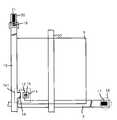
Translated fromKorean도 1은 통상의 엑스-선 검출소자의 패널을 도시한 도면.1 shows a panel of a conventional X-ray detection element.
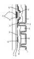
도 2은 종래의 엑스-선 검출소자를 도시한 평면도.2 is a plan view showing a conventional X-ray detection element.
도 3은 도 2에 도시된 화소영역의 수직구조를 나타내는 단면도.3 is a cross-sectional view illustrating a vertical structure of the pixel area illustrated in FIG. 2.
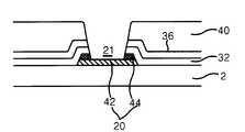
도 4는 도 2에 도시된 게이트패드부의 수직구조를 나타내는 단면도.4 is a cross-sectional view illustrating a vertical structure of the gate pad part illustrated in FIG. 2.
도 5는 도 2에 도시된 데이터패드부의 수직구조를 나타내는 단면도.5 is a cross-sectional view illustrating a vertical structure of the data pad unit shown in FIG. 2.
도 6은 도 2에 도시된 데이터링크부와 정전기 방지회로부의 게이트라인과 데이터라인 링크부의 수직구조를 나타내는 단면도.6 is a cross-sectional view illustrating a vertical structure of a gate line and a data line link unit of the data link unit and the antistatic circuit unit illustrated in FIG. 2.
도 7은 본 발명의 실시 예에 따른 엑스-선 검출소자를 도시한 평면도.7 is a plan view illustrating an X-ray detection device according to an embodiment of the present invention.
도 8a 내지 도 8f는 도 7에 도시된 엑스-선 검출소자의 제조방법을 단계적으로 도시한 단면도.8A through 8F are cross-sectional views illustrating a method of manufacturing the X-ray detection device illustrated in FIG. 7.
< 도면의 주요 부분에 대한 부호의 설명 ><Description of Symbols for Main Parts of Drawings>
2, 50 : 글라스 기판 3 : 게이트 라인2, 50: glass substrate 3: gate line
4 : 박막트랜지스터 기판 5 : 화소전극4 thin
6 : 광감지층 7 : 상부 유전층6
8 : 상부전극 9 : 고전압발생부8
10 : 데이터라인 12, 62 : 게이트전극10:
14,64 : 소스전극 15,17,19,21,63,65 : 컨택홀14,64
16,64 : 드레인전극 18 : 게이트패드16, 64
20 : 데이터패드 22, 52 : 그라운드 전극20:
32, 56, 58 : 게이트 절연막 34 : 반도체층32, 56, 58: gate insulating film 34: semiconductor layer
35 : 제1 투명전극 36, 54 : 스토리지 절연막35: first
38 : 제2 투명전극 40, 60 : 패시베이션층38: second
42 : 알루미늄층 44 : 몰리브덴층42: aluminum layer 44: molybdenum layer
66a : 비정질 실리콘층 66b : 다결정질 실리콘층66a:
본 발명은 엑스-선(이하 "X-선" 이라 함) 검출소자 및 그의 제조방법에 관한 것으로서, 특히 화소전극의 표면에 축적되는 전하의 수를 줄이기 위해 상기 화소전극 상에 형성되는 충전 블러킹 층으로 인한 추가공정을 줄이기 위한 엑스-선 검출소자 및 그의 제조방법에 관한 것이다.BACKGROUND OF THE INVENTION 1. Field of the Invention The present invention relates to an X-ray (hereinafter referred to as "X-ray") detection element and a method of manufacturing the same, and in particular, a charge blocking layer formed on the pixel electrode to reduce the number of charges accumulated on the surface of the pixel electrode. The present invention relates to an X-ray detection device and a method of manufacturing the same for reducing further processes.
피사체에 가시광이 아닌 X-선을 조사하여 이미지를 촬상하는 진단용 X-선 감지장치가 의료 분야에 폭넓게 이용되고 있다. 이러한 X-선 감지장치는 X-선을 검출하기 위한 검출소자가 필요하게 된다.Diagnostic X-ray detection apparatuses for imaging an image by irradiating X-rays instead of visible light on a subject have been widely used in the medical field. Such X-ray sensing apparatus requires a detection element for detecting X-rays.
최근, X-선 검출소자로 개발되고 있는 액티브 매트릭스 액정 표시소자(Active Matrix Liquid Crystal Display : 이하 "AMLCD"라 함)에 대한 연구가 활발히 진행되고 있다. AMLCD는 스위치 소자로서 박막트랜지스터(Thin Film Transistor : 이하 "TFT"라 함)를 이용하게 된다.Recently, research on an active matrix liquid crystal display (hereinafter referred to as "AMLCD"), which is being developed as an X-ray detection device, is being actively conducted. AMLCD uses a thin film transistor ("TFT") as a switch element.
도 1을 참조하면, X-선이 입사되는 광감지층(6)과, 유리기판(2) 상에 형성되어 광감지층(6)으로부터 검출된 X-선을 스위칭하기 위한 TFT 어레이(4)를 구비하는 AMLCD가 도시되어 있다. 광감지층(6)은 수백 ㎛ 두께의 셀레니옴(Selenium)이 TFT 어레이(4) 상에 도포되어 X-선을 전기적인 신호로 변환하는 역할을 하게 된다. 광감지층(6) 상에는 유전층(7)과 상부전극(8)이 형성된다. 상부전극(8)은 고전압 발생부(9)에 접속된다. TFT 어레이(4)는 게이트라인(3)을 경유하여 입력되는 제어신호에 응답하여 스토리지 캐패시터(Cst)에 충전된 전압신호를 데이터 재생부(도시하지 않음)에 전송하게 된다. 스토리지 캐패시터(Cst)는 TFT의 소오스전극과 기저전압원(GND) 사이에 접속되어 광감지층(6)으로부터 공급되는 신호를 충전하는 역할을 하게 된다.Referring to FIG. 1, a
피사체에 X-선이 조사되면, 피사체를 투과한 광은 광감지층(6)에 입사된다. 광감지층(6)에 입사된 X-선은 광감지층(6) 내에 전자-전공쌍을 생성시키게 된다. 고전압 발생부(9)로부터 발생되는 수 KV의 고전압이 상부전극(8)을 통하여 광감지층(6)에 인가되면 전자-정공쌍이 분리된다. 전자와 분리된 정공은 상부 화소전극(5)을 경유하여 스토리지 캐패시터(Cst)에 충전됨과 아울러 정공의 일부는 화소전극(5)의 표면상에 축적된다. 이로 인해, 스토리지 캐패시터(Cst)에 축적되 는 정공의 수가 감소하게 된다. 이를 방지하기 위해 화소전극(5) 상에는 화소전극(5)과 대응되게 충전 블러킹 층(Charge Blocking Layer)(11)이 형성된다. 또한, 게이트라인(3)을 경유하여 TFT의 게이트전극에 게이트전압이 인가되면 스토리지 캐패시터(Cst)에 충전된 전압이 드레인 전극을 통하여 데이터 재생부에 공급되어 영상으로 재생된다.When X-rays are irradiated to the subject, light passing through the subject is incident on the
도 2는 도 1에 도시된 TFT 어레이의 구조를 도시한 평면도이다.FIG. 2 is a plan view showing the structure of the TFT array shown in FIG.
도 2에 도시된 TFT 어레이에서 화소전극(5)은 게이트라인(3)과 데이터라인(10)에 의해 마련된 단위화소 영역에 형성된다. 스토리지 캐패시터(Cst)는 화소전극(5)과, 그 하부에 스토리지(Storage) 절연막(도시하지 않음)을 사이에 두고 위치하는 투명전극(도시하지 않음)에 의해 형성된다. 그라운드전극(22)은 스토리지 캐패시터(Cst)의 잔류전하를 리셋시키기 위한 것으로 화소전극(5)을 가로지르는 방향으로 형성된다. TFT는 데이터라인(10)과 게이트라인(3)의 교차지점에 형성된다. 이 TFT는 게이트라인(3)에서 연장된 게이트전극(12)과, 데이터라인(10)에서 연장된 드레인전극(16)과, 화소전극(5)과 컨택홀(15)에 의해 접속된 소스전극(14)과, 소스전극(14)과 드레인전극(16)에 접속된 반도체층(도시하지 않음)을 구성으로 한다. 게이트라인(3)과 데이터라인(10) 각각의 일측단에는 구동 IC(Integrated Circuit)와 접속되는 게이트패드부(18)와 데이터패드부(20) 각각이 형성된다. 게이트라인(3) 및 게이트전극(12)과 게이트패드(18)는 동일한 금속재질이 사용되며, 통상 알루미늄(Al)과 몰리브덴(Mo)이 순차적으로 적층된 구조를 가지고 있다. 데이터라인(10)은 신호전달 특성이 양호하도록 저항값을 줄이기 위하여 몰리브덴(Mo) 금속으로 이루어진다. 데이터패드(20)는 구동 IC와의 접속을 알루미늄(Al) 와이어 본딩(Wire bonding)으로 하기 위해 게이트패드(18)와 같이 알루미늄(Al)과 몰리브덴(Mo)이 적층된 구조를 가지고 있다. 이에 따라, 데이터패드(20)는 데이터라인(10)과 다른층에 형성되므로 게이트절연막(도시하지 않음)을 경유하여 형성된 컨택홀(19)을 통해 접속되게 된다. 게이트패드(18)와 데이터패드(20)는 컨택홀(17,21)을 통해 알루미늄(Al)의 금속층이 노출되어 구동 IC와 접속되게 된다.In the TFT array shown in FIG. 2, the
이러한 구조의 TFT 어레이의 제조방법을 도 3 내지 도 6을 참조하여 설명하기로 한다.A method of manufacturing a TFT array having such a structure will be described with reference to FIGS. 3 to 6.
우선적으로, 글라스 기판(2) 위에 증착공정을 이용하여 금속막을 형성한 후, 제1 마스크 패턴을 이용하여 패터닝함으로써 게이트라인(3)과 게이트전극(12), 게이트패드(18), 데이터패드(20)를 동시에 형성하게 된다. 이 경우, 게이트라인(3) 및 게이트전극(12), 게이트패드(18), 데이터패드(20)는 알루미늄(Al, 42)과 몰리브덴(Mo, 44) 금속이 순차적으로 적층된 구조를 가지게 된다. 게이트라인(3) 및 게이트전극(12) 등이 형성된 글라스 기판(2)의 전면에 연속적인 증착공정을 이용하여 게이트절연막(32)과 비정질실리콘(이하 "a-Si"라 함) 및 불순물이 도핑된 비정질 실리콘층(이하, "n+층"라 함)을 순차적으로 형성하게 된다. 그런 다음, 제2 마스크 패턴을 이용하여 n+층과 a-Si층을 패터닝함으로써 TFT의 채널을 형성하는 반도체층(34)을 형성하게 된다. 반도체층(34)을 형성한 후, 도 6에 도시된 바와 같이 게이트전극물질(Mo/Al)을 사용한 데이터패드(20)와 이후 형성될 데이터라인(10)과의 컨택을 위해 제3 마스크 패턴을 이용하여 데이터패드(20) 상의 게이트절연막(32)을 패터닝함으로써 컨택홀(19)을 형성하게 된다. 아울러, 정전기 방지회로에서의 게이트라인(3)과 데이터라인(10)과 접속을 위해 상기 제3 마스크 패턴을 이용한 동일한 사진식각 공정에 의해 게이트라인(3) 상의 게이트절연막(32)을 패터닝함으로써 컨택홀(도시하지 않음)을 형성하게 된다. 이러한 컨택홀(19)이 형성된 후 몰리브덴(Mo) 재질의 금속막을 형성하고 제4 마스크 패턴을 이용하여 패터닝함으로써 데이터라인(10) 및 소스전극(14)과 드레인전극(16), 그라운드 전극(22)을 형성하게 된다. 이 경우, 데이터링크부에서는 도 6에 도시된 바와 같이 몰리브덴(Mo) 재질의 데이터라인(10)과 몰리브덴/알루미늄(Mo/Al) 재질의 데이터패드(20)가 게이트절연막(32)에 형성된 컨택홀(19)을 통해 접속하게 된다. 아울러, 정전기방지회로부에서도 도 6에 도시된 바와 같이 몰리브덴(Mo) 재질의 데이터라인(10)과 몰리브덴/알루미늄(Mo/Al) 재질의 게이트라인(3)이 게이트절연막(32)에 형성된 컨택홀을 통해 접속하게 된다. 이어서, 투명전극물질을 전면 도포하고 제5 마스크 패턴을 이용하여 스토리지 캐패시터(Cst)를 위한 제1 투명전극(35)을 형성하게 된다. 이 제1 투명전극(35)이 형성된 후, 스토리지 캐패시터(Cst) 형성을 위한 스토리지 절연막(즉, 유전층)(36)을 전면 도포하게 된다. 이 스토리지 절연막(36) 상에 투명전극 물질을 전면 도포한 후 제6 마스크 패턴을 이용하여 제2 투명전극(38)을 형성하게 된다. 이 제2 투명전극(38)은 이후 형성될 패시베이션층(40)에 컨택홀을 형성하기 위해 에칭하는 경우 그 패시베이션층(40)의 에칭깊이를 제한하는 에치 스타퍼(Etch Stopper)의 역할을 하게 된다. 다시 말하여, 컨택홀 형성 시 패시베이션층(40)과 스토리지 절연막(36)을 보호해주는 역할을 하게 된다. 이 제2 투명전극(38)이 형성된 후, 전면에 무기 또는 유기 물질의 패시베이션층(40)을 형성하고 제7 마스크 패턴을 이용하여 패터닝함으로써 소스전극(14)과 화소전극(5)의 접속을 위한 컨택홀(15), 게이트패드(18) 및 데이터패드(20)와 구동 IC칩과의 접속을 위한 컨택홀(17,21), 화소전극(5)과 제2 투명전극(38)과의 접속을 위한 컨택홀을 형성하게 된다. 여기서, 소스전극(14)과 화소전극(5)의 접속을 위한 컨택홀(15)과, 게이트패드(18) 및 데이터패드(20) 각각과 구동 IC칩과의 접속을 위한 컨택홀(17,21)은 패시베이션층(40) 및 스토리지 절연막(36)을 경유하여 형성된다. 그리고, 투명전극 물질을 전면 도포한 후 제8 마스크 패턴을 이용하여 패터닝함으로써 화소전극(5)을 형성하게 된다. 이 화소전극(5)이 형성된 후 제9 마스크 패턴을 이용하여 게이트패드(18)와 데이터패드(20)의 컨택홀(17,21)을 통해 노출된 몰리브덴층(44)을 패터닝하여 알루미늄층(42)이 노출되게 한다. 이는 게이트 패드(18)와 데이터패드(20)를 구동 IC칩과 접착강도가 큰 알루미늄(Al) 와이어 본딩(Wire bonding)으로 접속시키기 위하여 알루미늄 구조로 가져가기 위한 것이다. 그런 다음, 화소전극(5)의 표면상에 정공이 축적되는 것을 방지함과 아울러 화소전극(5)을 보호하기 위해 화소전극(5) 전면에 충전 블러킹 층(11)이 형성된다.First, a metal film is formed on the
이와 같이 본 발명은 추가적으로 화소전극(5) 상에 충전 블러킹 층(11)을 형성함으로써 추가적인 공정이 필요하게 된다.
As such, the present invention requires an additional process by forming the
따라서, 본 발명의 목적은 화소전극의 표면에 축적되는 전하의 수를 줄이기 위해 상기 화소전극 상에 형성되는 충전 블러킹 층으로 인한 추가공정을 줄이기 위한 엑스-선 검출소자 및 그의 제조방법을 제공함에 있다.
Accordingly, an object of the present invention is to provide an X-ray detection device and a method of manufacturing the same for reducing an additional process due to the charge blocking layer formed on the pixel electrode in order to reduce the number of charges accumulated on the surface of the pixel electrode. .
상기 목적을 달성하기 위하여, 본 발명의 실시 예에 따른 엑스-선 검출소자는 글라스 기판과; 상기 글라스 기판 상에 형성되는 그라운드 전극과; 상기 그라운드 전극 상에 형성되는 스토리지 절연막과; 상기 스토리지 절연막 상에 형성되며 상기 그라운드 전극과 스토리지 캐패시터를 이루는 다결정 실리콘층 과; 상기 다결정 실리콘층 상에 형성되는 제1 게이트 절연막과; 상기 제1 게이트 절연막 상에 형성되는 게이트 전극과; 상기 게이트 전극 상에 형성되는 제2 게이트 절연막과; 상기 제1 및 제2 게이트 절연막을 경유하여 형성되는 제1 컨택홀과; 상기 제1 컨택홀을 통해 상기 다결정 실리콘층과 접속되도록 형성되는 소오스 및 드레인전극과; 상기 소오스 및 드레인전극 상에 형성되는 패시베이션층과; 상기 패시베이션층 및 제1 및 제2 게이트 절연막을 경유하여 상기 다결정 실리콘층이 외부로 노출되도록 하기 위한 제2 컨택홀을 구비한다.In order to achieve the above object, the X-ray detection device according to an embodiment of the present invention comprises a glass substrate; A ground electrode formed on the glass substrate; A storage insulating film formed on the ground electrode; A polycrystalline silicon layer formed on the storage insulating layer and forming a storage capacitor with the ground electrode; A first gate insulating film formed on the polycrystalline silicon layer; A gate electrode formed on the first gate insulating film; A second gate insulating film formed on the gate electrode; A first contact hole formed through the first and second gate insulating layers; Source and drain electrodes formed to be connected to the polycrystalline silicon layer through the first contact hole; A passivation layer formed on the source and drain electrodes; And a second contact hole for exposing the polycrystalline silicon layer to the outside via the passivation layer and the first and second gate insulating layers.
본 발명의 실시 예에 따른 엑스-선 검출소자의 제조방법은 상기 글라스 기판 상에 그라운드 전극을 형성하는 단계와; 상기 그라운드 전극 상에 스토리지 절연막을 형성하는 단계와; 상기 스토리지 절연막 상에 형성되어 상기 그라운드 전극과 스토리지 캐패시터를 이루는 다결정 실리콘층을 형성하는 단계와; 상기 다결정 실리콘층 상에 제1 게이트 절연막을 형성하는 단계와; 상기 게이트 절연막 상에 게이트 전극을 형성하는 단계와; 상기 게이트 전극 상에 제2 게이트 절연막을 형성하는 단계와; 상기 제1 및 제2 게이트 절연막을 경유하여 제1 컨택홀을 형성하는 단계와; 상기 제1 컨택홀을 통해 상기 다결정 실리콘층과 접속되도록 소오스 및 드레인전극을 형성하는 단계와; 상기 소오스 및 드레인전극 상에 패시베이션층을 형성하는 단계와; 상기 패시베이션층 및 제1 및 제2 게이트 절연막을 경유하여 상기 다결정 실리콘층이 외부로 노출되도록 하기 위해 제2 컨택홀을 형성하는 단계를 포함한다.Method of manufacturing an X-ray detection device according to an embodiment of the present invention comprises the steps of forming a ground electrode on the glass substrate; Forming a storage insulating layer on the ground electrode; Forming a polycrystalline silicon layer formed on the storage insulating layer to form a storage capacitor with the ground electrode; Forming a first gate insulating film on the polycrystalline silicon layer; Forming a gate electrode on the gate insulating film; Forming a second gate insulating film on the gate electrode; Forming a first contact hole via the first and second gate insulating layers; Forming a source and a drain electrode to be connected to the polycrystalline silicon layer through the first contact hole; Forming a passivation layer on the source and drain electrodes; And forming a second contact hole to expose the polycrystalline silicon layer to the outside via the passivation layer and the first and second gate insulating layers.
상기 목적 외에 본 발명의 다른 목적 및 특징들은 첨부도면을 참조한 실시 예에 대한 설명을 통하여 명백하게 드러나게 될 것이다.Other objects and features of the present invention in addition to the above object will be apparent from the description of the embodiments with reference to the accompanying drawings.
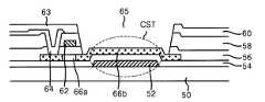
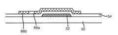
도 7은 본 발명의 실시 예에 따른 엑스-선 검출소자의 TFT 어레이부를 도시한 단면도이다.7 is a cross-sectional view illustrating a TFT array unit of an X-ray detection device according to an exemplary embodiment of the present invention.
도 7을 설명하면, 먼저 본 발명의 실시 예에 따른 엑스-선 검출소자의 TFT 어레이부는 글라스 기판(50) 상에 형성되는 그라운드 전극(52)과, 상기 그라운드 전극(52)을 덮도록 글라스 기판(50) 상에 형성되는 스토리지 절연막(54)과, 상기 스토리지 절연막(54) 상에 형성되는 a-Si층(66a) 및 p-Si층(66b)과, 상기 a-Si층(66a) 및 p-Si층(66b)을 덮도록 글라스 기판(50) 상에 형성되는 제1 게이트 절연막(56)과, a-Si층(66a)과 대응되게 상기 제1 게이트 절연막(56) 상에 형성되는 게이트 전극(62)과, 상기 게이트 전극(62)을 덮도록 글라스 기판(50) 상에 형성되는 제2 게이트 절연막(58)과, 이후 공정에 형성되는 소오스 및 드레인전극(64)이 p-Si층(66b)과 접촉되도록 상기 제1 및 제2 게이트 절연막(56,58)을 경유하여 형성 되는 제1 컨택홀(63)과, 상기 제1 컨택홀(63)을 통해 p-Si층(66b)과 접촉되도록 형성된 소오스 및 드레인전극(64)과, 상기 소오스 및 드레인전극(64)을 덮도록 글라스 기판(50) 상에 형성되는 패시베이션층(60)과, 이후 공정에 형성되는 a-Se(도시되지 않음)과 접촉됨과 아울러 p-Si층(66b)이 외부로 노출되기 위해 패시베이션층(60), 제2 및 제1 게이트절연막(58,56)을 경유하여 형성되는 제2 컨택홀(65)을 구비한다.Referring to FIG. 7, first, the TFT array unit of the X-ray detecting device according to the exemplary embodiment of the present disclosure may cover the
여기서, 스토리지 캐패시터(Cst)는 그라운드 전극(52), 스토리지 절연막(54) 및 p-Si층(66b)로 형성된다. 그라운드 전극(52)은 채널의 폭을 넓히기 위해 충분한 폭을 가지도록 형성된다. 스토리지 절연막(54)은 소정의 유전율(ε)을 갖도록 유기절연막이 이용된다. p-Si층(66b)은 a-Si층(66a)에 레이저 빔을 조사하여 다결정화시켜 반도체 특성을 갖도록 한다.Here, the storage capacitor Cst is formed of the
이를 도 8a 내지 도 8f를 결부하여 설명하면, 다음과 같다.This will be described with reference to FIGS. 8A to 8F.
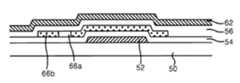
도 8a 내지 도 8f는 도 7에 도시된 엑스-선 검출소자의 TFT 어레이부의 제조방법을 단계적으로 상세히 도시한 단면도이다.8A to 8F are cross-sectional views illustrating in detail a method of manufacturing a TFT array unit of the X-ray detection device illustrated in FIG. 7.
도 8a를 참조하면, 먼저 엑스-선 검출소자의 TFT 어레이부는 글라스 기판(50) 상에 인듐 틴 옥사이드(Indium Tin Oxide : ITO)와 같은 투명전극을 전면에 증착한다. 그런 다음, 투명전극을 제1 마스크 패턴을 이용하여 에칭하면, 글라스 기판(50) 상에 그라운드 전극(52)이 형성된다. 이어서, 도 8b와 같이 글라스 기판(50) 상에 형성된 그라운드 전극(52)을 덮도록 스토리지 절연막(54)을 형성한다. 그런 다음, 스토리지 절연막(54) 상에 CVD(Chemical Vapor Deposition) 장비를 이용하여 a-Si를 전면 증착한 후, 400℃ 정도의 열처리로 수소를 이탈시키는 탈수소화 공정을 거치거나, 다이사일렌(Si2H6)을 이용하여 400~450℃ 정도에서 CVD 장비를 이용하여 a-Si를 증착한다. 이렇게 스토리지 절연막(54) 상에 증착된 a-Si 상부의 소정부분에만 마스크가 위치되도록 함과 아울러 그 상에 레이저 빛을 조사하여 빛에 노출된 부분만 결정화되도록 한다. 이때, 빛에 노출되어 결정화가 되는 부분은 도 8c에서도 도시된 바와 같이 그라운드 전극(52)과 대응되는 부분과 이 후 공정에서 소오스 및 드레인전극(64)이 접속되는 부분이다. 이와 같이 결정화가 되는 부분은 p-Si층(66b)이 되고, 결정화가 되지 않는 부분은 그대로 a-Si층(66a)으로 남게 된다. 이어서, 제2 마스크 패턴을 이용하여 p-Si층(66b)과 a-Si층(66a)이 스토리지 절연막(54)의 소정 부분에만 잔재하도록 패터닝한다. 그런 다음, 도 8d와 같이 패터닝되어 스토리지 절연막(54) 상의 소정 부분에 형성된 p-Si층(66b)과 a-Si층(66a) 상에는 제1 게이트 절연막(56) 및 금속전극이 순차적으로 증착된다. 여기서, 제1 게이트 절연막(56)은 유기절연막과 같은 유기물질로 구성된다. 또한, 금속전극은 몰리브덴(Mo), 크롬(Cr), 구리(Cu) 및 알루미늄(Al)등의 금속물질로 구성됨과 아울러 제3 마스크 패턴에 의해 패터닝되어 a-Si층(66a)과 대응되도록 제1 게이트 절연막(56) 상에 게이트 전극(62)이 도 8e와 같이 형성된다. 그런 다음, 게이트 전극(62)을 덮도록 제1 게이트 절연막(56) 상에는 제2 게이트 절연막(58)이 형성된다. 이어서, 도 8f와 같이 이 후 공정에서 형성되는 소오스 및 드레인전극(64)과 p-Si층(66b)이 접속되기 위해 제2 및 제1 게이트 절연막(58,56)은 제4 마스크 패턴에 의해 순차적으로 패터닝되어 그 부분에 제1 컨택홀(63)이 형성된다. 그런 다음, 제1 컨택홀(63)을 통해 p-Si층(66b)과 접속되도록 소오스 및 드레인전극(64)이 형성된다. 이어서, 소오스 및 드레인전극(64)이 형성된 글라스 기판(50) 상에 패시베이션층(60)을 전면 증착한 후, 제5 마스크 패턴을 이용하여 그라운드 전극(52)과 대응되게 형성된 p-Si층(66b)이 외부로 노출되도록 패시베이션층(60)이 패터닝된다. 이로 인해, 패시베이션층(60)이 패터닝되는 부분은 제2 컨택홀(65)이 형성된다.Referring to FIG. 8A, first, the TFT array unit of the X-ray detection element deposits a transparent electrode such as indium tin oxide (ITO) on the entire surface of the
이와 같이, 본 발명은 엑스-선 검출소자의 TFT 어레이부를 p형(p-type) p-Si로 형성함으로써, 종래 기술의 화소전극 상에 대응되게 추가적으로 형성된 충전 블러킹 층이 필요가 없게 된다. 이는, 그라운드 전극과 대응되게 형성된 p-Si층이 스토리지 캐패시터(Cst)로 동작함과 아울러 충전 블러킹 층의 역할을 대신할 수 있기 때문이다.
As described above, the present invention forms the TFT array portion of the X-ray detection element as p-type p-Si, thereby eliminating the need for a charge blocking layer additionally formed on the pixel electrode of the prior art. This is because the p-Si layer formed to correspond to the ground electrode may act as a storage capacitor Cst and may take the role of a charge blocking layer.
상술한 바와 같이, 본 발명의 실시 예에 따른 엑스-선 검출소자는 p형(p-type) p-Si를 이용하여 TFT 어레이부를 제조함으로써, 공정 단계가 감소될 수 있다.As described above, the X-ray detection device according to the exemplary embodiment of the present invention may reduce the process steps by manufacturing the TFT array unit using p-type p-Si.
이상 설명한 내용을 통해 당업자라면 본 발명의 기술사상을 일탈하지 아니하는 범위에서 다양한 변경 및 수정이 가능함을 알 수 있을 것이다. 따라서, 본 발명의 기술적 범위는 명세서의 상세한 설명에 기재된 내용으로 한정되는 것이 아니라 특허 청구의 범위에 의해 정하여 져야만 할 것이다.Those skilled in the art will appreciate that various changes and modifications can be made without departing from the technical spirit of the present invention. Therefore, the technical scope of the present invention should not be limited to the contents described in the detailed description of the specification but should be defined by the claims.
Claims (4)
Translated fromKoreanPriority Applications (1)
| Application Number | Priority Date | Filing Date | Title |
|---|---|---|---|
| KR1020000049902AKR100698238B1 (en) | 2000-08-26 | 2000-08-26 | X-ray detection device and manufacturing method thereof |
Applications Claiming Priority (1)
| Application Number | Priority Date | Filing Date | Title |
|---|---|---|---|
| KR1020000049902AKR100698238B1 (en) | 2000-08-26 | 2000-08-26 | X-ray detection device and manufacturing method thereof |
Publications (2)
| Publication Number | Publication Date |
|---|---|
| KR20020016714A KR20020016714A (en) | 2002-03-06 |
| KR100698238B1true KR100698238B1 (en) | 2007-03-21 |
Family
ID=19685438
Family Applications (1)
| Application Number | Title | Priority Date | Filing Date |
|---|---|---|---|
| KR1020000049902AExpired - LifetimeKR100698238B1 (en) | 2000-08-26 | 2000-08-26 | X-ray detection device and manufacturing method thereof |
Country Status (1)
| Country | Link |
|---|---|
| KR (1) | KR100698238B1 (en) |
Citations (4)
| Publication number | Priority date | Publication date | Assignee | Title |
|---|---|---|---|---|
| JPH05291293A (en)* | 1992-04-10 | 1993-11-05 | Casio Comput Co Ltd | Manufacture of thin film transistor |
| KR19980081122A (en)* | 1997-04-08 | 1998-11-25 | 모리시타요오이찌 | Thin film transistor, manufacturing method thereof and liquid crystal display device using the same |
| JPH1168109A (en)* | 1997-08-26 | 1999-03-09 | Matsushita Electric Ind Co Ltd | Method for manufacturing polycrystalline thin film and method for manufacturing thin film transistor |
| KR19990018394A (en)* | 1997-08-27 | 1999-03-15 | 윤종용 | Method of manufacturing polycrystalline silicon thin film transistor |
- 2000
- 2000-08-26KRKR1020000049902Apatent/KR100698238B1/ennot_activeExpired - Lifetime
Patent Citations (4)
| Publication number | Priority date | Publication date | Assignee | Title |
|---|---|---|---|---|
| JPH05291293A (en)* | 1992-04-10 | 1993-11-05 | Casio Comput Co Ltd | Manufacture of thin film transistor |
| KR19980081122A (en)* | 1997-04-08 | 1998-11-25 | 모리시타요오이찌 | Thin film transistor, manufacturing method thereof and liquid crystal display device using the same |
| JPH1168109A (en)* | 1997-08-26 | 1999-03-09 | Matsushita Electric Ind Co Ltd | Method for manufacturing polycrystalline thin film and method for manufacturing thin film transistor |
| KR19990018394A (en)* | 1997-08-27 | 1999-03-15 | 윤종용 | Method of manufacturing polycrystalline silicon thin film transistor |
Non-Patent Citations (1)
| Title |
|---|
| 1019980081122 |
Also Published As
| Publication number | Publication date |
|---|---|
| KR20020016714A (en) | 2002-03-06 |
Similar Documents
| Publication | Publication Date | Title |
|---|---|---|
| US6037609A (en) | Corrosion resistant imager | |
| US6607935B2 (en) | Method for fabricating array substrate for X-ray detector | |
| US20070109478A1 (en) | Method of fabricating an array substrate | |
| US6797961B2 (en) | X-ray detector and method of fabricating the same | |
| US6531346B1 (en) | Fabrication method of thin film transistor substrate for X-ray detector | |
| US20040183023A1 (en) | X-ray detector and method of fabricating therefore | |
| US6528819B2 (en) | Method of fabricating an array substrate for an x-ray detector | |
| KR20010066258A (en) | X-ray image sensor and a method for fabricating the same | |
| KR100310179B1 (en) | X-ray image sensor and a method for fabricating the same | |
| KR20100082631A (en) | X-ray detector and manufacturing method same of | |
| US6617584B2 (en) | X-ray detecting device and fabricating method thereof | |
| KR100463337B1 (en) | X-ray image sensor and mothed for fabricating the same | |
| KR20000061396A (en) | X-ray image decector and a method for fabricating the same | |
| KR100730066B1 (en) | X-ray detection device and manufacturing method thereof | |
| KR100351440B1 (en) | X-Ray Detecting Device and Fabricating Method Thereof | |
| US7268366B2 (en) | Method of fabricating X-ray detecting device | |
| KR100698238B1 (en) | X-ray detection device and manufacturing method thereof | |
| EP0890190B1 (en) | Corrosion resistant imager | |
| KR100683526B1 (en) | X-ray detection device and manufacturing method thereof | |
| WO1998032173A9 (en) | Corrosion resistant imager | |
| KR100463594B1 (en) | A X-ray detector and a method for fabricating thereof | |
| CA2247717A1 (en) | Corrosion resistant imager |
Legal Events
| Date | Code | Title | Description |
|---|---|---|---|
| PA0109 | Patent application | Patent event code:PA01091R01D Comment text:Patent Application Patent event date:20000826 | |
| N231 | Notification of change of applicant | ||
| PN2301 | Change of applicant | Patent event date:20010328 Comment text:Notification of Change of Applicant Patent event code:PN23011R01D | |
| PG1501 | Laying open of application | ||
| A201 | Request for examination | ||
| PA0201 | Request for examination | Patent event code:PA02012R01D Patent event date:20050825 Comment text:Request for Examination of Application Patent event code:PA02011R01I Patent event date:20000826 Comment text:Patent Application | |
| E902 | Notification of reason for refusal | ||
| PE0902 | Notice of grounds for rejection | Comment text:Notification of reason for refusal Patent event date:20060830 Patent event code:PE09021S01D | |
| E701 | Decision to grant or registration of patent right | ||
| PE0701 | Decision of registration | Patent event code:PE07011S01D Comment text:Decision to Grant Registration Patent event date:20070212 | |
| GRNT | Written decision to grant | ||
| PR0701 | Registration of establishment | Comment text:Registration of Establishment Patent event date:20070315 Patent event code:PR07011E01D | |
| PR1002 | Payment of registration fee | Payment date:20070316 End annual number:3 Start annual number:1 | |
| PG1601 | Publication of registration | ||
| PR1001 | Payment of annual fee | Payment date:20091218 Start annual number:4 End annual number:4 | |
| PR1001 | Payment of annual fee | Payment date:20101228 Start annual number:5 End annual number:5 | |
| PR1001 | Payment of annual fee | Payment date:20111221 Start annual number:6 End annual number:6 | |
| FPAY | Annual fee payment | Payment date:20121228 Year of fee payment:7 | |
| PR1001 | Payment of annual fee | Payment date:20121228 Start annual number:7 End annual number:7 | |
| FPAY | Annual fee payment | Payment date:20131227 Year of fee payment:8 | |
| PR1001 | Payment of annual fee | Payment date:20131227 Start annual number:8 End annual number:8 | |
| FPAY | Annual fee payment | Payment date:20150227 Year of fee payment:9 | |
| PR1001 | Payment of annual fee | Payment date:20150227 Start annual number:9 End annual number:9 | |
| FPAY | Annual fee payment | Payment date:20160226 Year of fee payment:10 | |
| PR1001 | Payment of annual fee | Payment date:20160226 Start annual number:10 End annual number:10 | |
| PR1001 | Payment of annual fee | Payment date:20170215 Start annual number:11 End annual number:11 | |
| FPAY | Annual fee payment | Payment date:20180213 Year of fee payment:12 | |
| PR1001 | Payment of annual fee | Payment date:20180213 Start annual number:12 End annual number:12 | |
| PR1001 | Payment of annual fee | Payment date:20190215 Start annual number:13 End annual number:13 | |
| FPAY | Annual fee payment | Payment date:20200219 Year of fee payment:14 | |
| PR1001 | Payment of annual fee | Payment date:20200219 Start annual number:14 End annual number:14 | |
| PC1801 | Expiration of term |