KR100695662B1 - Process for Forming Semiconductor Structure - Google Patents
Process for Forming Semiconductor StructureDownload PDFInfo
- Publication number
- KR100695662B1 KR100695662B1KR1020027010316AKR20027010316AKR100695662B1KR 100695662 B1KR100695662 B1KR 100695662B1KR 1020027010316 AKR1020027010316 AKR 1020027010316AKR 20027010316 AKR20027010316 AKR 20027010316AKR 100695662 B1KR100695662 B1KR 100695662B1
- Authority
- KR
- South Korea
- Prior art keywords
- layer
- single crystal
- delete delete
- compound semiconductor
- silicon
- Prior art date
- Legal status (The legal status is an assumption and is not a legal conclusion. Google has not performed a legal analysis and makes no representation as to the accuracy of the status listed.)
- Expired - Lifetime
Links
Images


Classifications
- H—ELECTRICITY
- H01—ELECTRIC ELEMENTS
- H01S—DEVICES USING THE PROCESS OF LIGHT AMPLIFICATION BY STIMULATED EMISSION OF RADIATION [LASER] TO AMPLIFY OR GENERATE LIGHT; DEVICES USING STIMULATED EMISSION OF ELECTROMAGNETIC RADIATION IN WAVE RANGES OTHER THAN OPTICAL
- H01S5/00—Semiconductor lasers
- H01S5/02—Structural details or components not essential to laser action
- H01S5/026—Monolithically integrated components, e.g. waveguides, monitoring photo-detectors, drivers
- H01S5/0261—Non-optical elements, e.g. laser driver components, heaters
- H—ELECTRICITY
- H10—SEMICONDUCTOR DEVICES; ELECTRIC SOLID-STATE DEVICES NOT OTHERWISE PROVIDED FOR
- H10D—INORGANIC ELECTRIC SEMICONDUCTOR DEVICES
- H10D84/00—Integrated devices formed in or on semiconductor substrates that comprise only semiconducting layers, e.g. on Si wafers or on GaAs-on-Si wafers
- H10D84/01—Manufacture or treatment
- H10D84/02—Manufacture or treatment characterised by using material-based technologies
- H10D84/05—Manufacture or treatment characterised by using material-based technologies using Group III-V technology
- C—CHEMISTRY; METALLURGY
- C30—CRYSTAL GROWTH
- C30B—SINGLE-CRYSTAL GROWTH; UNIDIRECTIONAL SOLIDIFICATION OF EUTECTIC MATERIAL OR UNIDIRECTIONAL DEMIXING OF EUTECTOID MATERIAL; REFINING BY ZONE-MELTING OF MATERIAL; PRODUCTION OF A HOMOGENEOUS POLYCRYSTALLINE MATERIAL WITH DEFINED STRUCTURE; SINGLE CRYSTALS OR HOMOGENEOUS POLYCRYSTALLINE MATERIAL WITH DEFINED STRUCTURE; AFTER-TREATMENT OF SINGLE CRYSTALS OR A HOMOGENEOUS POLYCRYSTALLINE MATERIAL WITH DEFINED STRUCTURE; APPARATUS THEREFOR
- C30B25/00—Single-crystal growth by chemical reaction of reactive gases, e.g. chemical vapour-deposition growth
- C30B25/02—Epitaxial-layer growth
- C30B25/18—Epitaxial-layer growth characterised by the substrate
- H—ELECTRICITY
- H01—ELECTRIC ELEMENTS
- H01L—SEMICONDUCTOR DEVICES NOT COVERED BY CLASS H10
- H01L21/00—Processes or apparatus adapted for the manufacture or treatment of semiconductor or solid state devices or of parts thereof
- H01L21/02—Manufacture or treatment of semiconductor devices or of parts thereof
- H01L21/02104—Forming layers
- H01L21/02365—Forming inorganic semiconducting materials on a substrate
- H01L21/02367—Substrates
- H01L21/0237—Materials
- H01L21/02373—Group 14 semiconducting materials
- H01L21/02381—Silicon, silicon germanium, germanium
- H—ELECTRICITY
- H01—ELECTRIC ELEMENTS
- H01L—SEMICONDUCTOR DEVICES NOT COVERED BY CLASS H10
- H01L21/00—Processes or apparatus adapted for the manufacture or treatment of semiconductor or solid state devices or of parts thereof
- H01L21/02—Manufacture or treatment of semiconductor devices or of parts thereof
- H01L21/02104—Forming layers
- H01L21/02365—Forming inorganic semiconducting materials on a substrate
- H01L21/02367—Substrates
- H01L21/02433—Crystal orientation
- H—ELECTRICITY
- H01—ELECTRIC ELEMENTS
- H01L—SEMICONDUCTOR DEVICES NOT COVERED BY CLASS H10
- H01L21/00—Processes or apparatus adapted for the manufacture or treatment of semiconductor or solid state devices or of parts thereof
- H01L21/02—Manufacture or treatment of semiconductor devices or of parts thereof
- H01L21/02104—Forming layers
- H01L21/02365—Forming inorganic semiconducting materials on a substrate
- H01L21/02436—Intermediate layers between substrates and deposited layers
- H01L21/02439—Materials
- H01L21/02469—Group 12/16 materials
- H01L21/02472—Oxides
- H—ELECTRICITY
- H01—ELECTRIC ELEMENTS
- H01L—SEMICONDUCTOR DEVICES NOT COVERED BY CLASS H10
- H01L21/00—Processes or apparatus adapted for the manufacture or treatment of semiconductor or solid state devices or of parts thereof
- H01L21/02—Manufacture or treatment of semiconductor devices or of parts thereof
- H01L21/02104—Forming layers
- H01L21/02365—Forming inorganic semiconducting materials on a substrate
- H01L21/02436—Intermediate layers between substrates and deposited layers
- H01L21/02439—Materials
- H01L21/02488—Insulating materials
- H—ELECTRICITY
- H01—ELECTRIC ELEMENTS
- H01L—SEMICONDUCTOR DEVICES NOT COVERED BY CLASS H10
- H01L21/00—Processes or apparatus adapted for the manufacture or treatment of semiconductor or solid state devices or of parts thereof
- H01L21/02—Manufacture or treatment of semiconductor devices or of parts thereof
- H01L21/02104—Forming layers
- H01L21/02365—Forming inorganic semiconducting materials on a substrate
- H01L21/02436—Intermediate layers between substrates and deposited layers
- H01L21/02494—Structure
- H01L21/02496—Layer structure
- H01L21/02505—Layer structure consisting of more than two layers
- H01L21/02507—Alternating layers, e.g. superlattice
- H—ELECTRICITY
- H01—ELECTRIC ELEMENTS
- H01L—SEMICONDUCTOR DEVICES NOT COVERED BY CLASS H10
- H01L21/00—Processes or apparatus adapted for the manufacture or treatment of semiconductor or solid state devices or of parts thereof
- H01L21/02—Manufacture or treatment of semiconductor devices or of parts thereof
- H01L21/02104—Forming layers
- H01L21/02365—Forming inorganic semiconducting materials on a substrate
- H01L21/02436—Intermediate layers between substrates and deposited layers
- H01L21/02494—Structure
- H01L21/02513—Microstructure
- H—ELECTRICITY
- H01—ELECTRIC ELEMENTS
- H01L—SEMICONDUCTOR DEVICES NOT COVERED BY CLASS H10
- H01L21/00—Processes or apparatus adapted for the manufacture or treatment of semiconductor or solid state devices or of parts thereof
- H01L21/02—Manufacture or treatment of semiconductor devices or of parts thereof
- H01L21/02104—Forming layers
- H01L21/02365—Forming inorganic semiconducting materials on a substrate
- H01L21/02518—Deposited layers
- H01L21/02521—Materials
- H01L21/02538—Group 13/15 materials
- H01L21/02543—Phosphides
- H—ELECTRICITY
- H01—ELECTRIC ELEMENTS
- H01L—SEMICONDUCTOR DEVICES NOT COVERED BY CLASS H10
- H01L21/00—Processes or apparatus adapted for the manufacture or treatment of semiconductor or solid state devices or of parts thereof
- H01L21/02—Manufacture or treatment of semiconductor devices or of parts thereof
- H01L21/02104—Forming layers
- H01L21/02365—Forming inorganic semiconducting materials on a substrate
- H01L21/02518—Deposited layers
- H01L21/02521—Materials
- H01L21/02538—Group 13/15 materials
- H01L21/02546—Arsenides
- H—ELECTRICITY
- H10—SEMICONDUCTOR DEVICES; ELECTRIC SOLID-STATE DEVICES NOT OTHERWISE PROVIDED FOR
- H10D—INORGANIC ELECTRIC SEMICONDUCTOR DEVICES
- H10D84/00—Integrated devices formed in or on semiconductor substrates that comprise only semiconducting layers, e.g. on Si wafers or on GaAs-on-Si wafers
- H10D84/01—Manufacture or treatment
- H10D84/02—Manufacture or treatment characterised by using material-based technologies
- H10D84/08—Manufacture or treatment characterised by using material-based technologies using combinations of technologies, e.g. using both Si and SiC technologies or using both Si and Group III-V technologies
- H—ELECTRICITY
- H10—SEMICONDUCTOR DEVICES; ELECTRIC SOLID-STATE DEVICES NOT OTHERWISE PROVIDED FOR
- H10H—INORGANIC LIGHT-EMITTING SEMICONDUCTOR DEVICES HAVING POTENTIAL BARRIERS
- H10H29/00—Integrated devices, or assemblies of multiple devices, comprising at least one light-emitting semiconductor element covered by group H10H20/00
- H10H29/10—Integrated devices comprising at least one light-emitting semiconductor component covered by group H10H20/00
- H—ELECTRICITY
- H01—ELECTRIC ELEMENTS
- H01L—SEMICONDUCTOR DEVICES NOT COVERED BY CLASS H10
- H01L21/00—Processes or apparatus adapted for the manufacture or treatment of semiconductor or solid state devices or of parts thereof
- H01L21/02—Manufacture or treatment of semiconductor devices or of parts thereof
- H01L21/02104—Forming layers
- H01L21/02107—Forming insulating materials on a substrate
- H01L21/02109—Forming insulating materials on a substrate characterised by the type of layer, e.g. type of material, porous/non-porous, pre-cursors, mixtures or laminates
- H01L21/02112—Forming insulating materials on a substrate characterised by the type of layer, e.g. type of material, porous/non-porous, pre-cursors, mixtures or laminates characterised by the material of the layer
- H01L21/02172—Forming insulating materials on a substrate characterised by the type of layer, e.g. type of material, porous/non-porous, pre-cursors, mixtures or laminates characterised by the material of the layer the material containing at least one metal element, e.g. metal oxides, metal nitrides, metal oxynitrides or metal carbides
- H01L21/02197—Forming insulating materials on a substrate characterised by the type of layer, e.g. type of material, porous/non-porous, pre-cursors, mixtures or laminates characterised by the material of the layer the material containing at least one metal element, e.g. metal oxides, metal nitrides, metal oxynitrides or metal carbides the material having a perovskite structure, e.g. BaTiO3
- H—ELECTRICITY
- H01—ELECTRIC ELEMENTS
- H01L—SEMICONDUCTOR DEVICES NOT COVERED BY CLASS H10
- H01L21/00—Processes or apparatus adapted for the manufacture or treatment of semiconductor or solid state devices or of parts thereof
- H01L21/02—Manufacture or treatment of semiconductor devices or of parts thereof
- H01L21/02104—Forming layers
- H01L21/02107—Forming insulating materials on a substrate
- H01L21/02225—Forming insulating materials on a substrate characterised by the process for the formation of the insulating layer
- H01L21/0226—Forming insulating materials on a substrate characterised by the process for the formation of the insulating layer formation by a deposition process
- H01L21/02263—Forming insulating materials on a substrate characterised by the process for the formation of the insulating layer formation by a deposition process deposition from the gas or vapour phase
- H01L21/02271—Forming insulating materials on a substrate characterised by the process for the formation of the insulating layer formation by a deposition process deposition from the gas or vapour phase deposition by decomposition or reaction of gaseous or vapour phase compounds, i.e. chemical vapour deposition
- H01L21/0228—Forming insulating materials on a substrate characterised by the process for the formation of the insulating layer formation by a deposition process deposition from the gas or vapour phase deposition by decomposition or reaction of gaseous or vapour phase compounds, i.e. chemical vapour deposition deposition by cyclic CVD, e.g. ALD, ALE, pulsed CVD
- H—ELECTRICITY
- H01—ELECTRIC ELEMENTS
- H01L—SEMICONDUCTOR DEVICES NOT COVERED BY CLASS H10
- H01L21/00—Processes or apparatus adapted for the manufacture or treatment of semiconductor or solid state devices or of parts thereof
- H01L21/02—Manufacture or treatment of semiconductor devices or of parts thereof
- H01L21/02104—Forming layers
- H01L21/02365—Forming inorganic semiconducting materials on a substrate
- H01L21/02518—Deposited layers
- H01L21/02521—Materials
- H01L21/02551—Group 12/16 materials
- H01L21/02557—Sulfides
- H—ELECTRICITY
- H01—ELECTRIC ELEMENTS
- H01L—SEMICONDUCTOR DEVICES NOT COVERED BY CLASS H10
- H01L21/00—Processes or apparatus adapted for the manufacture or treatment of semiconductor or solid state devices or of parts thereof
- H01L21/02—Manufacture or treatment of semiconductor devices or of parts thereof
- H01L21/02104—Forming layers
- H01L21/02365—Forming inorganic semiconducting materials on a substrate
- H01L21/02518—Deposited layers
- H01L21/02521—Materials
- H01L21/02551—Group 12/16 materials
- H01L21/0256—Selenides
- H—ELECTRICITY
- H01—ELECTRIC ELEMENTS
- H01L—SEMICONDUCTOR DEVICES NOT COVERED BY CLASS H10
- H01L2924/00—Indexing scheme for arrangements or methods for connecting or disconnecting semiconductor or solid-state bodies as covered by H01L24/00
- H01L2924/0001—Technical content checked by a classifier
- H01L2924/0002—Not covered by any one of groups H01L24/00, H01L24/00 and H01L2224/00
- H—ELECTRICITY
- H01—ELECTRIC ELEMENTS
- H01S—DEVICES USING THE PROCESS OF LIGHT AMPLIFICATION BY STIMULATED EMISSION OF RADIATION [LASER] TO AMPLIFY OR GENERATE LIGHT; DEVICES USING STIMULATED EMISSION OF ELECTROMAGNETIC RADIATION IN WAVE RANGES OTHER THAN OPTICAL
- H01S5/00—Semiconductor lasers
- H01S5/02—Structural details or components not essential to laser action
- H01S5/0206—Substrates, e.g. growth, shape, material, removal or bonding
- H01S5/021—Silicon based substrates
- H—ELECTRICITY
- H10—SEMICONDUCTOR DEVICES; ELECTRIC SOLID-STATE DEVICES NOT OTHERWISE PROVIDED FOR
- H10H—INORGANIC LIGHT-EMITTING SEMICONDUCTOR DEVICES HAVING POTENTIAL BARRIERS
- H10H20/00—Individual inorganic light-emitting semiconductor devices having potential barriers, e.g. light-emitting diodes [LED]
- H10H20/80—Constructional details
- H10H20/81—Bodies
- H10H20/817—Bodies characterised by the crystal structures or orientations, e.g. polycrystalline, amorphous or porous
- H—ELECTRICITY
- H10—SEMICONDUCTOR DEVICES; ELECTRIC SOLID-STATE DEVICES NOT OTHERWISE PROVIDED FOR
- H10H—INORGANIC LIGHT-EMITTING SEMICONDUCTOR DEVICES HAVING POTENTIAL BARRIERS
- H10H20/00—Individual inorganic light-emitting semiconductor devices having potential barriers, e.g. light-emitting diodes [LED]
- H10H20/80—Constructional details
- H10H20/81—Bodies
- H10H20/822—Materials of the light-emitting regions
- H10H20/824—Materials of the light-emitting regions comprising only Group III-V materials, e.g. GaP
Landscapes
- Engineering & Computer Science (AREA)
- Physics & Mathematics (AREA)
- Condensed Matter Physics & Semiconductors (AREA)
- General Physics & Mathematics (AREA)
- Manufacturing & Machinery (AREA)
- Computer Hardware Design (AREA)
- Microelectronics & Electronic Packaging (AREA)
- Power Engineering (AREA)
- Chemical & Material Sciences (AREA)
- Crystallography & Structural Chemistry (AREA)
- Materials Engineering (AREA)
- General Chemical & Material Sciences (AREA)
- Chemical Kinetics & Catalysis (AREA)
- Electromagnetism (AREA)
- Metallurgy (AREA)
- Organic Chemistry (AREA)
- Optics & Photonics (AREA)
- Recrystallisation Techniques (AREA)
- Semiconductor Memories (AREA)
- Metal-Oxide And Bipolar Metal-Oxide Semiconductor Integrated Circuits (AREA)
- Bipolar Integrated Circuits (AREA)
- Junction Field-Effect Transistors (AREA)
- Crystals, And After-Treatments Of Crystals (AREA)
- Semiconductor Lasers (AREA)
- Semiconductor Integrated Circuits (AREA)
- Bipolar Transistors (AREA)
- Formation Of Insulating Films (AREA)
- Solid State Image Pick-Up Elements (AREA)
Abstract
Translated fromKoreanDescription
Translated fromKorean본 발명은 일반적으로 반도체 구조들을 형성하기 위한 공정에 관한 것으로, 특히, 화합물 반도체 구조들을 형성하기 위한 공정 및 단결정 화합물 반도체 재료를 포함하는 반도체 구조들의 이용에 관한 것이다.The present invention relates generally to a process for forming semiconductor structures, and more particularly, to a process for forming compound semiconductor structures and to the use of semiconductor structures comprising a single crystal compound semiconductor material.
대부분의 반도체 이산 장치들 및 집적 회로들은 저가의 고품질 단결정 실리콘 기판들의 유용성으로 인해 적어도 부분적으로 실리콘으로 제조된다. 소위 화합물 반도체 재료들과 같은 다른 반도체 재료들은 보다 넓은 밴드갭 및/또는 실리콘보다 높은 모빌리티 또는 이들 재료들이 특정 타입의 반도체 장치에 대해 유익한 직접적인 밴드갭들을 포함하는 물리적 속성들을 가진다. 바람직하지 않게, 화합물 반도체 재료들은 실리콘보다 보다 고가이고 실리콘과는 달리 큰 웨이퍼들로 이용할 수 없다. 가장 쉽게 이용할 수 있는 화합물 반도체 재료인 갈륨 비소(GaAs)는 직경 약 150 밀리미터(mm) 까지의 웨이퍼들로 이용할 수 있다. 대조하여, 실리콘 웨이퍼들은 약 300 mm까지 이용할 수 있고 200mm에서 폭넓게 사용된다. 150mm GaAs 웨이퍼들은 대응하는 실리콘보다 몇 배나 더 고가 이다. 다른 화합물 반도체 재료들의 웨이퍼들은 구입하기 어렵고 GaAs보다 더 고가이다.Most semiconductor discrete devices and integrated circuits are at least partially made of silicon due to the availability of low cost, high quality single crystal silicon substrates. Other semiconductor materials, such as so-called compound semiconductor materials, have wider bandgaps and / or higher mobility than silicon or physical properties that include direct bandgaps where these materials are beneficial for certain types of semiconductor devices. Undesirably, compound semiconductor materials are more expensive than silicon and unlike silicon are not available with larger wafers. Gallium arsenide (GaAs), the most readily available compound semiconductor material, is available for wafers up to about 150 millimeters in diameter. In contrast, silicon wafers are available up to about 300 mm and are widely used at 200 mm. 150mm GaAs wafers are many times more expensive than their corresponding silicon. Wafers of other compound semiconductor materials are difficult to purchase and are more expensive than GaAs.
화합물 반도체 재료들의 바람직한 특성, 및 고비용 및 벌크 형태에서의 낮은 이용 가능성으로 인해, 지난 몇 년간 외부 기판상에 화합물 반도체 재료의 얇은 막을 성장시키기 위한 시도가 이루어졌다. 그러나, 화합물 반도체 재료의 최적 특성을 달성하기 위하여, 높은 결정 품질의 단결정 막이 요구된다. 예를 들어, 게르마늄, 실리콘, 및 다양한 절연체상에 단결정 화합물 반도체 재료층을 성장시키는 것이 시도되었다. 이들 시도들은 성공하지 못하였는데, 그 이유는 호스트 결정과 성장된 결정 사이의 격자 부정합이 낮은 결정 품질을 갖는 화합물 반도체 재료의 최종 얇은 막을 유발하기 때문이다.Due to the desirable properties of compound semiconductor materials, and their high cost and low availability in bulk form, attempts have been made in the last few years to grow thin films of compound semiconductor materials on external substrates. However, in order to achieve the optimum properties of the compound semiconductor material, a high crystal quality single crystal film is required. For example, it has been attempted to grow a single crystal compound semiconductor material layer on germanium, silicon, and various insulators. These attempts were unsuccessful because the lattice mismatch between the host crystal and the grown crystal results in a final thin film of compound semiconductor material with low crystal quality.
고품질의 단결정 화합물 반도체 재료의 넓은 영역의 얇은 막이 저비용으로 이용될 수 있으면, 다양한 반도체 장치들은 화합물 반도체 재료의 벌크 웨이퍼 상이나, 화합물 반도체 재료의 벌크 웨이퍼 상에 있는 상기 재료의 에피텍셜 막에 상기 장치들을 제조하는 비용에 비해 저비용으로 상기 얇은 막 상에 제조될 수 있다. 게다가, 고품질 단결정 화합물 반도체 재료의 얇은 막이 실리콘 웨이퍼 같은 벌크 웨이퍼 상에서 실현될 수 있으면, 집적된 장치 구조는 실리콘과 화합물 반도체 재료 양쪽의 가장 좋은 특성의 장점을 가지도록 구성될 수 있다.If a thin film of a large area of high quality single crystal compound semiconductor material is available at low cost, various semiconductor devices may be used to deposit the devices on an epitaxial film of the material on a bulk wafer of compound semiconductor material or on a bulk wafer of compound semiconductor material. It can be produced on the thin film at low cost compared to the cost of manufacturing. In addition, if a thin film of high quality single crystal compound semiconductor material can be realized on a bulk wafer such as a silicon wafer, the integrated device structure can be configured to take advantage of the best properties of both silicon and compound semiconductor material.
따라서, 다른 단결정 재료 위에 고품질 단결정 화합물 반도체 막을 제공하는 반도체 구조를 제조하는 공정에 대한 필요성이 존재한다.Thus, there is a need for a process for producing a semiconductor structure that provides a high quality single crystal compound semiconductor film over another single crystal material.
본 발명은 첨부 도면으로 제한되지 않고 예시적으로 도시되며, 동일 참조부호는 동일한 요소들을 가리킨다.The invention is illustrated by way of example and not by way of limitation in the figures of the drawings, in which like reference characters designate like elements.
당업자는 도면의 요소가 간략화 및 명확화를 위하여 도시되고 비례적으로 도시되지 않았다는 것을 인식할 것이다. 예를 들어, 도면에서 몇몇 요소의 크기는 본 발명의 실시에의 이해를 촉진하기 위하여 다른 요소에 비해 과장되게 도시된다.Those skilled in the art will recognize that elements of the figures are shown for simplicity and clarity and not to scale. For example, the dimensions of some of the elements in the drawings are exaggerated compared to other elements to facilitate understanding of the practice of the present invention.
도 1은 본 발명의 실시예에 따른 반도체 구조(20)의 일부를 개략적으로 단면으로 도시한다. 반도체 구조(20)는 단결정 기판(22), 단결정 재료를 포함하는 수용 버퍼층(24), 및 단결정 화합물 반도체 재료층(26)을 포함한다. 이것과 관련하여, 용어 "단결정(monocrystalline)"은 반도체 산업에서 일반적으로 사용되는 의미를 가진다. 상기 용어는 단일 결정 또는 실질적으로 단일 결정인 재료들을 말하고, 반도체 산업에서 통상적으로 발견되는 실리콘 또는 게르마늄 또는 실리콘과 게르마늄의 혼합물들의 기판들 및 그러한 재료들의 애픽택셜층에서 통상적으로 발견되는 비교적 적은 수의 전위(dislocation) 등과 같은 결함을 가진 재료를 포함한다.1 schematically illustrates in cross section a portion of a
본 발명의 일 실시예에 따라, 구조(20)는 기판(22)과 수용 버퍼층(24) 사이에 배치된 비정질 중간층(28)을 또한 포함한다. 구조(20)는 수용 버퍼층과 화합물 반도체 층(26) 사이에 템플레이트 층(30)을 또한 포함한다. 이하에서 보다 상세히 설명될 바와 같이, 템플레이트 층은 수용 버퍼층상에 화합물 반도체 층의 성장을 시작하는 것을 돕는다. 비정질 중간층은 수용 버퍼층에서 스트레인(strain)을 경감시키고 이렇게 함으로써 고품질의 결정질의 수용 버퍼층 성장을 돕는다.According to one embodiment of the invention, the
본 발명의 일 실시예에 따른 기판(22)은 바람직하게 큰 직경의 단결정 반도체 웨이퍼이다. 웨이퍼는 주기율표의 그룹 Ⅳ 재료이고 바람직하게 그룹 ⅣA 재료이다. 그룹 Ⅳ 반도체 재료는 실리콘, 게르마늄, 혼합된 실리콘 및 게르마늄, 혼합된 실리콘 및 탄소, 혼합된 실리콘, 게르마늄 및 탄소 등을 포함한다. 바람직하게 기판(22)은 실리콘 또는 게르마늄을 포함하는 웨이퍼이고, 가장 바람직하게 반도체 산업에서 사용되는 고품질 단결정 실리콘 웨이퍼이다. 수용 버퍼층(24)은 바람직하게 하부 기판상에서 애피텍셜 성장된 단결정 산화물 또는 질화물 재료이다. 본 발명의 일 실시예에 따라, 비정질 중간층(28)은 기판(22)과 성장하는 수용 버퍼층 간의 인터페이스에 층(24)의 성장동안 기판(22)의 산화에 의해 기판(22)상에 성장된다. 비정질 중간층은 기판과 버퍼층의 격자 상수 차이로 인해 단결정 버퍼층에서 발생할 수 있는 스트레인을 경감하기 위하여 사용한다. 여기에 사용된 바와 같이, 격자 상수는 기판 평면에서 측정된 셀의 원자들 간의 거리이다. 상기 스트레인이 비정질 중간층에 의해 경감되지 않으면, 스트레인은 수용 버퍼층의 결정 구조에 결함을 유발할 수 있다. 이어서, 수용 버퍼층의 결정 구조의 결함은 단결정 화합물 반도체 층(26)에서 고품질 결정 구조를 달성하기 어렵게 만든다.The
수용 버퍼층(24)은 하부 기판 및 상부 화합물 반도체 층(25)과의 결정 호환성을 위해 선택된 단결정 산화물 또는 질화물 재료인 것이 바람직하다. 예를 들어, 상기 재료는 기판 및 이어서 인가되는 반도체 재료에 정합되는 격자 구조를 가지는 산화물 또는 질화물일 수 있다. 수용 버퍼층에 적당한 재료는 알카리 토금속 티타네이트, 알카리 토금속 지르코네이트, 알카리 토금속 하프네이트, 알카리 토금속 탄탈레이트, 알카리 토금속 루데네이트, 알카리 토금속 니오베이트, 알카리 토금속 바나데이트, 알카리 토금속 주석 기반 페로브스카이트, 란타늄 알루미네이트, 란타늄 스칸듐 산화물, 및 가돌리늄 산화물 같은 금속 산화물을 포함한다. 부가적으로, 갈륨 질화물, 알루미늄 질화물, 및 붕소 질화물 같은 다양한 질화물이 수용 버퍼층으로 사용될 수 있다. 이들 재료들은, 비록 스트론튬 루데네이트가 도전체일지라도 대부분 절연체이다. 일반적으로, 이들 재료들은 금속 산화물 또는 금속 질화물이고, 보다 구체적으로 이들 금속 산화물 또는 질화물은 적어도 두 개의 다른 금속 원소들을 포함한다. 특정 응용에서, 금속 산화물 또는 질화물은 3개 이상의 다른 금속 원소들을 포함할 수 있다.The
비정질 인퍼테이스 층(28)은 기판(22) 표면의 산화에 의해 형성된 산화물인 것이 바람직하고 실리콘 산화물로 구성되는 것이 더 바람직하다. 층(28)의 두께는 기판(22)과 수용 버퍼층(24)의 격자 상수 사이의 부정합을 일으키는 스트레인을 경감하기에 충분하다. 통상적으로, 층(28)은 대략 0.5 내지 5nm 범위의 두께를 가진다.It is preferable that the
층(26)의 화합물 반도체 재료는 특정 반도체 기판을 위한 요구에 따라 그룹 ⅢA 및 VA 원소들(Ⅲ-Ⅴ 반도체 화합물), 혼합된 Ⅲ-Ⅴ 화합물, 그룹 Ⅱ(A 또는 B), VIA 원소들(Ⅱ-Ⅵ 반도체 화합물), 및 혼합된 Ⅱ-Ⅵ 화합물 중 어느 하나로부터 선택된다. 예는 갈륨 비소화물(GaAs), 갈륨 인듐 비소화물(GaInAs), 갈륨 알루미늄 비소화물(GaAlAs), 인듐 인화물(InP), 카드뮴 황화물(CdS), 카드뮴 머큐리 텔루르 화합물(CdHgTe), 아연 셀렌 화합물(ZnSe), 아연 황 셀렌 화합물(ZnSSe) 등을 포함한다. 적당한 템플레이트 재료는 선택된 사이트에서 수용 버퍼층(24)의 표면에 화학적으로 본딩되고 추후 화합물 반도체 층(26)의 에피텍셜 성장의 핵화(nucleation)를 위한 사이트를 제공한다. 템플레이트(30)에 적당한 재료는 하기된다.The compound semiconductor material of
도 2는 본 발명의 추가 실시예에 따른 반도체 구조(40)의 일부를 단면으로 도시한다. 구조(40)는 부가적인 버퍼층(32)이 수용 버퍼층(24)과 단결정 화합물 반도체 재료(26)의 층 사이에 배치되는 것을 제외하면 이전에 기술된 반도체 구조(20)와 동일하다. 특히, 부가적인 버퍼층은 템플레이트 층(30)과 화합물 반도체 재료의 상부층 사이에 배치된다. 반도체 또는 화합물 반도체 재료로 형성된 부가적인 버퍼층은 수용 버퍼층의 격자 상수가 상부 단결정 화합물 반도체 재료층에 적당하게 정합될 수 없을 때 격자 보상을 제공하기 위하여 사용한다.2 shows in cross section a portion of a
다음의 비제한적이고 도시적인 실시예는 본 발명의 다양한 다른 실시예에 따라 구조(20) 및 구조(40)에 사용되는 재료의 다양한 결합물을 도시한다. 이들 실시예는 단순히 도시를 위한 것이고, 본 발명이 이들 도시적인 실시예에 제한되는 것으로 의도되지는 않는다.The following non-limiting, illustrative embodiments illustrate various combinations of materials used in
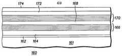
도 1, 도 2, 도 4, 및 도 5는 본 발명의 여러 실시예에 따른 장치 구조를 개략적으로 도시한 단면도.1, 2, 4, and 5 are schematic cross-sectional views of device structures in accordance with various embodiments of the present invention.
도 3은 호스트 결정과 성장된 결정 상부층 사이의 격자 부정합과 최대 달성 가능한 막 두께 사이의 관계를 그래프로 도시한 도.3 graphically illustrates the relationship between lattice mismatch between a host crystal and a grown crystal top layer and the maximum achievable film thickness.
도 6은 통신 장치의 일부의 블록도.6 is a block diagram of a portion of a communication device.
도 7 내지 도 11은 화합물 반도체 부분, 바이폴라 부분, 및 MOS 부분을 포함하는 집적 회로의 일부의 단면도.7-11 are cross-sectional views of a portion of an integrated circuit that includes a compound semiconductor portion, a bipolar portion, and a MOS portion.
도 12 내지 도 18은 반도체 층과 MOS 트랜지스터를 포함하는 다른 집적 회로의 일부의 단면을 도시한 도.12-18 illustrate cross-sections of portions of other integrated circuits including semiconductor layers and MOS transistors.
실시예 1Example 1
본 발명의 일 실시예에 따라 단결정 기판(22)은 (100) 방향으로 향한 실리콘 기판이다. 실리콘 기판은 약 200 내지 300mm의 직경을 가진 상보적 금속 산화물 반도체(CMOS) 집적 회로를 제조하는데 일반적으로 사용되는 실리콘 기판이다. 본 발명의 이 실시예에 따라, 수용 버퍼층(24)은 SRzBa1-zTiO3의 단결정 층이고, 여기서 z는 0 내지 1 범위이고 비정질 중간층은 실리콘 기판과 수용 버퍼층 사이의 인터페이스에 형성된 실리콘 산화물(SiOx)이다. z의 값은 추후 형성된 층(26)의 대응 격자 상수에 근접하게 정합되는 하나 이상의 격자 상수를 얻도록 선택된다. 수용 버퍼층은 약 2 내지 약 100 나노미터(nm)의 두께 및 바람직하게 약 10nm의 두께를 가진다. 일반적으로, 목표된 전기 및 광학 특성을 얻기 위하여 기판으로부터 화합물 반도체 층을 절연시키기에 충분한 수용 버퍼층 두께를 가지는 것이 바람직하다. 100nm보다 두꺼운 층은 불필요하게 가격을 증가시키면서 작은 부가적인 이익을 제공하지만; 보다 두꺼운 층은 요구에 따라 제조될 수 있다. 실리콘 산화물의 비정질 중간층은 약 0.5 내지 5nm의 두께, 및 바람직하게 약 1.5 내지 2.5nm의 두께를 가진다.According to one embodiment of the invention, the
본 발명의 이와 같은 실시예에 따라, 화합물 반도체 재료 층(26)은 약 1nm 내지 약 100 마이크로미터(㎛) 및 바람직하게 약 0.5 ㎛ 내지 10㎛의 두께를 가진 갈륨 비소화물(GaAs) 또는 알루미늄 갈륨 비소화물(AlGaAs) 층이다. 두께는 층이 제공되는 응용에 따른다. 단결정 산화물상 갈륨 비소화물 또는 알루미늄 갈륨 비소화물의 에피텍셜 성장을 용이하게 하기 위하여, 템플레이트 층은 산화물 층을 덮음으로써 형성된다. 템플레이트 층은 Ti-As, Sr-0-As, Sr-Ga-O, 또는 Sr-Al-O의 1-10 단층들이다. 바람직한 실시예에 의해, Ti-As 또는 Sr-Ge-O의 1-2 단층들은 GaAs 층을 성공적으로 성장시키는 것을 나타난다.According to this embodiment of the present invention, compound
실시예 2Example 2
본 발명의 다른 실시예에 따라, 단결정 기판(22)은 상기된 바와 같이 실리콘 기판이다. 수용 버퍼층은 실리콘 기판 및 수용 버퍼층 사이의 인터페이스에 형성된 실리콘 산화물의 비정질 중간층과 동위상의 입방체 또는 사방정계의 스트론튬 단결정 산화물 또는 바륨 지르코네이트 또는 하프네이트이다. 수용 버퍼층은 약 2 내지 100 nm의 두께를 가지며 바람직하게 적당한 결정 및 표면 품질을 보장하기 위하여 적어도 5nm의 두께를 가지며 단결정 SrZrO3, BaZrO3, SrHfO3, BaSnO3 또는 BaHfO3으로 형성된다. 예를 들어, BaZrO3의 단결정 산화물 층은 약 700도의 온도에서 성장될 수 있다. 결과적인 결정 산화물의 격자 구조는 기판 실리콘 격자 구조에 비해 45 도 회전을 나타낸다.According to another embodiment of the present invention, the
이들 지르코네이트 또는 하프네이트 재료로 형성된 수용 버퍼층은 인듐 인화물(InP) 시스템의 화합물 반도체 재료 성장에 적당하다. 화합물 반도체 재료는 예를 들어 약 1.0 nm 내지 10 ㎛의 두께를 가진 인듐 인화물(InP) 또는 인듐 갈륨 비소화물(InGaAs)이다. 이 구조에 적당한 템플레이트는 지르코늄 비소(Zr-As), 지르코늄-인(Zr-P), 하프늄-비소(Hf-As), 하프늄-인(Hf-P), 스트론튬-산소-비소(Sr-O-As), 스트론튬-산소-인(Sr-O-P), 바륨-산소-비소(Ba-O-As), 인듐-스트론튬-산소(In-Sr-O), 또는 바륨-산소-인(Ba-O-P)의 단층, 및 바람직하게 이들 재료 중 하나의 1-2 단층들이다. 예를 들어, 바륨 지르코네이트 수용 버퍼 지르코늄을 위해, 표면은 Zr-As 템플레이트를 형성하도록 지르코늄의 1-2 단층들로 증착되고 그 다음 비소의 1-2 단층들을 증착한다. 인듐 인 시스템으로부터 화합물 반도체 재료의 단결정 층은 템플레이트 층상에서 성장한다. 화합물 반도체 재료의 결과적인 격자 구조는 수용 버퍼층 격자 구조에 대해 45 도 회전과 및 2.5% 이하, 및 바람직하게 약 1.0% 이하의 (100) InP에 대한 격자 부정합을 나타낸다.The receiving buffer layer formed of these zirconate or hafnate materials is suitable for growing compound semiconductor materials of indium phosphide (InP) systems. Compound semiconductor materials are, for example, indium phosphide (InP) or indium gallium arsenide (InGaAs) having a thickness of about 1.0 nm to 10 μm. Suitable templates for this structure include zirconium arsenic (Zr-As), zirconium-phosphorus (Zr-P), hafnium-arsenic (Hf-As), hafnium-phosphorus (Hf-P), strontium-oxygen-arsenic (Sr-O) -As), strontium-oxygen-phosphorus (Sr-OP), barium-oxygen-arsenic (Ba-O-As), indium-strontium-oxygen (In-Sr-O), or barium-oxygen-phosphorus (Ba- Monolayers of OP), and preferably 1-2 monolayers of one of these materials. For example, for barium zirconate receiving buffer zirconium, the surface is deposited with 1-2 monolayers of zirconium and then 1-2 monolayers of arsenic to form a Zr-As template. The monocrystalline layer of compound semiconductor material from the indium phosphorus system grows on the template layer. The resulting lattice structure of the compound semiconductor material exhibits a 45 degree rotation with respect to the receiving buffer layer lattice structure and lattice mismatch to (100) InP of 2.5% or less, and preferably about 1.0% or less.
실시예 3Example 3
본 발명의 다른 실시예에 따라, 구조는 실리콘 기판상 Ⅱ-Ⅵ 재료의 에피텍셜 막의 성장에 적당하게 제공된다. 기판은 상기된 바와 같이 실리콘 웨이퍼이다. 적당한 수용 버퍼층 재료는 SrxBa1-xTiO3이고, 여기서 x는 약 2 내지 100 nm의 두께 및 바람직하게 약 5 내지 15 nm의 두께를 가진 0 내지 1 범위이다. Ⅱ-Ⅵ 화합물 반도체 재료는 예를 들어 아연 셀렌 화합물(ZnSe) 또는 아연 황 셀렌 화합물(ZnSSe)이다. 이런 재료 시스템에 대하여 적당한 템플레이트는 아연 산소(Zn-O)의 1-10 단층들 다음 아연의 초과 1-2 단층들 다음 표면상 아연의 셀렌화를 포함한다. 선택적으로, 템플레이트는 스트론튬-황(Sr-S) 다음 ZnSeS일 수 있다.According to another embodiment of the present invention, the structure is suitably provided for the growth of an epitaxial film of II-VI material on a silicon substrate. The substrate is a silicon wafer as described above. Suitable receiving buffer layer materials are Srx Ba1-x TiO3 , where x is in the range 0-1 with a thickness of about 2 to 100 nm and preferably a thickness of about 5 to 15 nm. II-VI compound semiconductor materials are, for example, zinc selenium compounds (ZnSe) or zinc sulfur selenium compounds (ZnSSe). Suitable templates for this material system include selenization of zinc on the surface following 1-10 monolayers of zinc oxygen (Zn-O) followed by excess 1-2 monolayers of zinc. Optionally, the template may be ZnSeS followed by strontium-sulfur (Sr-S).
실시예 4Example 4
본 발명의 이 실시예는 도 2에 도시된 구조(40)의 예이다. 기판(22), 단결정 산화물 층(24) 및 단결정 화합물 반도체 재료층(26)은 실시예 1에 기술된 것과 유사하다. 게다가 부가적인 버퍼층(32)은 수용 버퍼층의 결정 격자와 단결정 반도체 재료의 격자의 부정합으로부터 발생하는 어떤 스트레인을 경감시키기 위하여 사용한다. 버퍼층(32)은 갈륨 비소 인(GaAsxP1-x) 또는 인듐 갈륨 인(InyGa1-yP) 스트레인 보상 초격자이다. 갈륨 비소화물 인 초격자에서 x의 값은 0 내지 1이고, 인듐 갈륨 인 초격자에서 y의 값은 0 내지 1 범위이다. x 또는 y의 값을 가변시킴으로써, 격자 상수는 하부 산화물 및 상부 화합물 반도체 재료의 격자 상수 사이의 정합을 형성하기 위하여 초격자를 가로질러 하부에서 상부로 가변된다. 초격자는 약 50 내지 500nm의 두께를 가지며 바람직하게 약 200 내지 100nm의 두께를 가진다. 이 구조에 대한 템플레이트는 실시예 1에 기술된 바와 동일하다. 선택적으로, 버퍼층은 1 내지 50 nm의 두께를 가진 단결정 게르마늄 층이고 바람직하게 약 2 내지 20 nm의 두께를 가진다. 게르마늄 버퍼층 사용 시, 약 1 단층 두께를 가진 게르마늄 스트론튬(Ge-Sr) 또는 게르마늄 티타늄(Ge-Ti)중 어느 하나의 템플레이트 층이 사용된다. 산화물 층의 형성은 스트론튬 단층 또는 단결정 게르마늄의 추후 증착을 위한 핵 사이트로서 작동하기 위한 티타늄 단층 중 어느 하나로 덮여진다. 스트론튬 또는 티타늄의 단층은 게르마늄의 제 1 단층이 본딩되는 핵 사이트를 제공한다.This embodiment of the present invention is an example of the
실시예 5Example 5
이 실시예는 도 2에 도시된 바와 같이 구조(40)에 이용하는 재료를 도시한다. 기판 재료(22), 수용 버퍼층(24), 단결정 화합물 반도체 재료층(26) 및 템플 레이트 층(30)은 실시예에 기술된 바와 같다. 게다가, 버퍼층(32)은 수용 버퍼층 및 단결정 화합물 반도체 재료층 사이에 삽입된다. 버퍼층, 추가 단결정 반도체 재료는 예를 들어 인듐 화합물이 약 0 내지 47% 사이에서 가변하는 인듐 갈륨 비소화물(InGaAs)의 등급 층이다. 버퍼층은 바람직하게 약 10 내지 30 nm의 두께를 가진다. GaAs로부터 InGaAs로 버퍼층의 조성물을 가변시키는 것은 하부 단결정 산화물 재료와 단결정 화합물 반도체 재료의 상부층 사이에 격자 정합을 제공하기 위하여 사용한다. 상기 버퍼층은 만약 수용 버퍼층(24)과 단결정 화합물 반도체 재료층(26) 사이에 격자 부정합이 있다면 특히 바람직하다.This embodiment illustrates the material used for
도 1 및 도 2를 다시 참조하여, 기판(22)은 단결정 실리콘 기판 같은 단결정 기판이다. 단결정 기판의 결정 구조는 격자 상수 및 격자 방향을 특징으로 한다. 유사한 방식으로, 수용 버퍼층(24)은 단결정 재료이고 단결정 재료의 격자는 격자 상수 및 격자 방향을 특징으로 한다. 수용 버퍼층 및 단결정 기판의 격자 상수는 비슷하게 정합되어야 하거나 선택적으로 다른 결정 방향에 대해 하나의 결정 방향의 회전 후 격자 상수의 실질적인 정합이 달성되도록 되어야 한다. 이것과 관련하여 용어 "실질적 동일(substantially equal)" 및 "실질적 정합(substantially matched)"은 하부 층상 고품질 결정 층의 성장을 허용하도록 격자 상수 사이에 충분한 유사성이 있다는 것을 의미한다.Referring back to FIGS. 1 and 2, the
도 3은 호스 결정 및 성장된 결정의 격자 상수 사이의 부정합에 의해 고품질의 결정으로 성장된 결정 층의 달성 가능한 두께 관계를 그래프로 도시한다. 곡선(42)의 고품질 결정 재료 경계를 도시한다. 곡선(42)의 우측 영역은 다결정과 같은 층을 나타낸다. 격자 부정합없이, 이론적으로 무한히 두꺼운 고품질 에피텍 셜층을 호스트 결정 상에 성장시키는 것이 가능하다. 격자 상수의 부정합이 증가할 때, 달성 가능한 고품질 결정 층의 두께는 빠르게 감소한다. 기준 포인트로서, 예를 들어, 호스트 격자 및 성장된 층 사이의 격자 상수가 약 2%보다 많이 부정합되면, 약 20 nm 초과되는 단결정 에피텍셜층은 달성될 수 없다.3 graphically illustrates achievable thickness relationships of crystal layers grown with high quality crystals by mismatches between the lattice constants of the hose crystals and grown crystals. The high quality crystalline material boundary of the
본 발명의 일 실시예에 따라, 기판(22)은 (100) 또는 (111) 방향 단결정 실리콘 웨이퍼이고 수용 버퍼층(24)은 스트론튬 바륨 티타네이트 층이다. 이들 두 개의 재료 사이의 격자 상수의 실제 정합은 실리콘 기판 웨이퍼의 결정 방향에 대해 45 도만큼 티타네이트의 결정 방향을 회전시킴으로써 달성된다. 비정질 인터페이스 층(24) 구조에서의 함유물인 실리콘 산화물 층은 호스트 실리콘 웨이퍼 및 성장된 티타네이트 층의 격자 상수 부정합을 유발하는 티타네이트 단결정 층의 스트레인을 감소시키기 위하여 사용한다. 결과적으로, 본 발명의 일 실시예에 따라, 고품질의 두꺼운 단결정 티타네이트 층은 달성될 수 있다.According to one embodiment of the invention, the
도 1 및 도 2를 참조하여, 층(26)은 에피텍셜적으로 성장된 단결정 화합물 반도체 재료층이고 결정 재료는 결정 격자 상수 및 결정 방향을 특징으로 한다. 이 에피텍셜적으로 성장된 층에서 고품질 결정을 달성하기 위하여, 수용 버퍼층은 고품질 결정이어야 한다. 게다가, 층(26)에서 고품질 결정을 달성하기 위하여, 호스트 결정, 이 경우 단결정 수용 버퍼층, 및 성장된 결정 사이의 실제 정합은 목표된다. 적당하게 선택된 재료로, 이 격자 상수의 실제 정합은 호스트 결정 방향에 대해 성장된 결정의 결정 방향을 회전함으로써 달성된다. 만약 성장된 결정이 갈륨 비소화물, 알루미늄 갈륨 비소화물, 아연 셀렌 화합물, 또는 아연 황 셀렌 화합물이거나 수용 버퍼층이 단결정 SrxBa1-xTiO3이면, 두 개의 재료의 결정 격자 상수의 실제적 정합은 달성되고, 여기서 성장된 층의 결정 방향은 호스트 단결정 산화물의 방향에 대해 45 도 회전된다. 유사하게, 만약 호스트 재료가 스트론튬 또는 바륨 지르코네이트 또는 스트론튬 또는 바륨 하프네이트 또는 바륨 주석 산화물이고 화합물 반도체 층이 인듐 인 또는 갈륨 인듐 비소화물 또는 알루미늄 인듐 비소화물이면, 결정 격자 상수의 실제 정합은 호스트 산화물 결정에 대해 성장된 결정 층의 방향을 45도 만큼 회전시킴으로써 달성된다. 몇몇 예에서, 호스트 산화물 및 성장된 화합물 반도체 층 사이의 결정 반도체 버퍼층은 격자 상수의 작은 차로부터 발생하는 성장된 단결정 화합물 반도체 층의 스트레인을 감소시키기 위하여 사용된다. 따라서 보다 우수한 품질의 성장된 단결정 화합물 반도체의 결정은 달성된다.1 and 2,
다음 실시예는 도 1 및 도 2에 도시된 구조 같은 반도체 구조를 제조하기 위한 본 발명의 일 실시예에 따른 공정을 도시한다. 상기 공정은 실리콘 또는 게르마늄을 포함하는 단결정 반도체 기판을 제공함으로써 시작된다. 본 발명의 바람직한 실시예에 따라, 반도체 기판은 (100) 방향을 가진 실리콘 웨이퍼이다. 기판은 바람직하게 축 방향 또는 거의 약 0.5 벗어난 축 방향을 가진다. 적어도 일부분의 반도체 기판은 비록 하기될 기판의 다른 부분이 다른 구조를 포함할 수 있을지라도 베어(bare) 표면을 가진다. 이 문맥에서 용어 "베어(bare)"는 기판 부분의 표면이 어떤 산화물, 오염물, 또는 다른 외부 재료를 제거하기 위하여 세척되었다는 것을 의미한다. 잘 알려진 바와 같이, 베어 실리콘은 반응성이고 쉽게 네이티브 산화물을 형성한다. 용어 "베어"는 상기 네이티브 산화물을 포함한다. 얇은 실리콘 산화물은 비록 상기 성장된 산화물이 본 발명에 따른 공정에서 필수적이지는 않지만 반도체 기판상에 고의적으로 성장될 수 있다. 단결정 기판 상부에 단결정 산화물 층을 에피텍셜적으로 성장시키기 위하여, 네이티브 산화물 층은 우선 하부 기판의 결정 구조를 노출시키기 위하여 제거되어야 한다. 다음 공정은 분자 빔 에피텍시(MBE)에 의해 수행된다. 네이티브 산화물은 MBE 장치에서 스트론튬의 얇은 층을 열적으로 증착함으로써 제거될 수 있다. 기판은 네이티브 실리콘 산화물 층과 스트론튬이 반응하도록 하는 약 750 도의 온도로 가열된다. 스트론튬은 실리콘 산화물 없는 표면을 남기기 위하여 실리콘 산화물을 감소시키는데 사용한다. 2X1 구조를 나타내는 결과적인 표면은 스트론튬, 산소, 및 실리콘을 포함한다. 순차적 2X1 구조는 단결정 산화물의 상부층에 순차적 성장을 위한 템플레이트를 형성한다. 템플레이트는 필요한 화학 및 물리적 특성을 제공하여 상부층의 결정 성장을 증가시킨다.The following example illustrates a process according to one embodiment of the present invention for producing a semiconductor structure, such as the structure shown in FIGS. 1 and 2. The process begins by providing a single crystal semiconductor substrate comprising silicon or germanium. According to a preferred embodiment of the invention, the semiconductor substrate is a silicon wafer with a (100) orientation. The substrate preferably has an axial direction or an axial direction that is about 0.5 off. At least a portion of the semiconductor substrate has a bare surface, although other portions of the substrate to be described below may include other structures. The term "bare" in this context means that the surface of the substrate portion has been cleaned to remove any oxides, contaminants, or other foreign material. As is well known, bare silicon is reactive and easily forms native oxides. The term "bare" includes such native oxides. Thin silicon oxide can be intentionally grown on a semiconductor substrate although the grown oxide is not essential to the process according to the present invention. In order to epitaxially grow a single crystal oxide layer on top of a single crystal substrate, the native oxide layer must first be removed to expose the crystal structure of the underlying substrate. The next process is performed by molecular beam epitaxy (MBE). Native oxides can be removed by thermally depositing a thin layer of strontium in the MBE device. The substrate is heated to a temperature of about 750 degrees to allow the native silicon oxide layer and strontium to react. Strontium is used to reduce silicon oxide to leave a surface free of silicon oxide. The resulting surface showing the 2 × 1 structure includes strontium, oxygen, and silicon. The sequential 2 × 1 structure forms a template for sequential growth on the top layer of single crystal oxide. The template provides the necessary chemical and physical properties to increase crystal growth of the top layer.
본 발명의 다른 실시예에 따라, 네이티브 실리콘 산화물은 컨버트되고 기판 표면은 저온에서 MBE에 의해 기판 표면 위에 스트론튬 산화물을 증착하고 약 750 도의 온도로 상기 구조를 추후 가열함으로써 단결정 산화물 층의 성장을 위해 제공된다. 이 온도에서 고체 상태 반응은 네이티브 실리콘 산화물의 감소를 유발하고 스트론튬 산소, 및 기판 표면상에 남아있는 실리콘을 가진 순차적 2X1 구조를 남김으로써 스트론튬 산화물 및 네이티브 실리콘 사이에서 발생한다. 다시, 이것은 순차적 단결정 산화물 층의 추후 성장을 위한 템플레이트를 형성한다.According to another embodiment of the present invention, the native silicon oxide is converted and the substrate surface is provided for growth of a single crystal oxide layer by depositing strontium oxide on the substrate surface by MBE at low temperature and subsequently heating the structure to a temperature of about 750 degrees. do. Solid state reactions at this temperature occur between strontium oxide and native silicon, causing a decrease in native silicon oxide and leaving a sequential 2 × 1 structure with strontium oxygen, and silicon remaining on the substrate surface. Again, this forms a template for later growth of the sequential single crystal oxide layer.
기판의 표면에서 실리콘 산화물을 제거한 후, 본 발명의 일 실시예에 따라, 기판은 약 400 내지 600도 범위의 온도로 냉각되고 스트론튬 티타네이트 층은 분바 빔 에피텍시에 의해 템플레이트 층상에 성장된다. MBE 공정은 스트론튬, 티타늄 및 산소 소스를 노출시키기 위하여 ME 장치의 개구 셔터에 의해 시작된다. 스트론튬 및 티타늄의 비율은 대략 1:1이다. 산소의 부분 압력은 분당 약 0.3 내지 0.5 nm의 성장 속도로 통계적 스트론튬 티타네이트를 성장시키기 위하여 최소 값으로 처음에 설정된다. 스트론튬 티타네이트의 처음 성장 후, 산소의 부분압력은 초기 최소 값 이상으로 증가된다. 산소의 과압력은 하부 기판 및 성장된 스트론튬 티타네이트 층 사이 인터페이스에서 비정질 실리콘 산화물의 성장을 유발한다. 실리콘 산화물 층의 성장은 성장된 스트론튬 티타네이트 층을 통하여 산소가 하부 기판의 표면 실리콘과 반응하는 인터페이스로 산소의 확산을 유발한다. 스트론튬 티타네이트는 하부 기판의 순차적 2X1 결정 구조에 대해 45도 만큼 회전된 결정 방향을 가진 순차적 단결정으로서 성장한다. 실리콘 기판과 성장 결정 사이의 격자 상수의 작은 부정합으로 인한 스트론튬 티타네이트 층에 존재하는 스트레인은 비정질 산화물 중간층으로 경감된다.After removing the silicon oxide from the surface of the substrate, in accordance with one embodiment of the present invention, the substrate is cooled to a temperature in the range of about 400 to 600 degrees and the strontium titanate layer is grown on the template layer by Bunbar beam epitaxy. The MBE process is initiated by an aperture shutter in the ME device to expose strontium, titanium and oxygen sources. The ratio of strontium and titanium is approximately 1: 1. The partial pressure of oxygen is initially set to the minimum value for growing statistical strontium titanate at a growth rate of about 0.3 to 0.5 nm per minute. After the initial growth of strontium titanate, the partial pressure of oxygen is increased above the initial minimum value. The overpressure of oxygen causes the growth of amorphous silicon oxide at the interface between the underlying substrate and the grown strontium titanate layer. Growth of the silicon oxide layer causes the diffusion of oxygen through the grown strontium titanate layer to an interface where oxygen reacts with the surface silicon of the underlying substrate. Strontium titanate grows as a sequential single crystal with a crystal orientation rotated by 45 degrees relative to the sequential 2 × 1 crystal structure of the underlying substrate. The strain present in the strontium titanate layer due to the small mismatch of lattice constant between the silicon substrate and the growth crystals is alleviated to the amorphous oxide interlayer.
스트론튬 티타네이트 층이 목표된 두께로 성장된 후, 단결정 스트론튬 티타네이트는 목표된 화합물 반도체 재료 에피텍셜층의 추후 성장을 위한 템플레이트 층에 의해 덮여진다. 갈륨 비소화물 층의 추후 성장을 위하여, 스트론튬 티타네이트 단결정 층의 MBE 성장은 티타늄의 1-2 단층들, 티타늄 산소의 1-2 단층들 또는 스트론튬 산소의 1-2 단층들로 성장을 멈춤으로써 덮여진다. 이런 덮는 층의 형성 후, 비소는 Ti-As 본딩, Ti-O-As 본딩 또는 Sr-O-As를 형성하기 위하여 증착된다. 이들 중 어떤 것은 갈륨 비소화물 단결정 층의 증착 및 형성을 위한 적당한 템플레이트를 형성한다. 템플레이트 형성 후, 갈륨은 비소 및 갈륨 비소화물 형태와 반응을 위해 도입된다. 선택적으로, 갈륨은 Sr-O-Ga 본딩을 형성하기 위하여 덮는 층상에 증착되고, 비소는 GaAs를 형성하기 위하여 갈륨과 함께 도입된다.After the strontium titanate layer is grown to the desired thickness, the single crystal strontium titanate is covered by a template layer for later growth of the target compound semiconductor material epitaxial layer. For later growth of the gallium arsenide layer, the MBE growth of the strontium titanate single crystal layer is covered by stopping growth with 1-2 monolayers of titanium, 1-2 monolayers of titanium oxygen, or 1-2 monolayers of strontium oxygen. Lose. After formation of this covering layer, arsenic is deposited to form Ti-As bonding, Ti-O-As bonding or Sr-O-As. Some of these form suitable templates for the deposition and formation of gallium arsenide single crystal layers. After template formation, gallium is introduced for reaction with arsenic and gallium arsenide forms. Optionally, gallium is deposited on the covering layer to form Sr-O-Ga bonding, and arsenic is introduced together with gallium to form GaAs.
도 2에 도시된 구조는 부가적인 버퍼층 증착 단계의 부가와 함께 상기 공정에 의해 형성된다. 버퍼층은 단결정 화합물 반도체 층의 증착 전에 템플레이트 층 상부에 형성된다. 만약 버퍼층이 화합물 반도체 초격자이면, 상기 초격자는 예를 들어 MBE에 의해 템플레이트 상에 증착된다. 만약 버퍼층이 게르마늄 층이면, 상기 공정은 스트론튬 또는 티타늄의 최종 층으로 스트론튬 티타네이트 단결정 층을 덮고 스트론튬 또는 티타늄과 반응하도록 게르마늄을 증착하도록 변형된다. 게르마늄 버퍼층은 이 템플레이트 상에 바로 증착된다.The structure shown in FIG. 2 is formed by this process with the addition of an additional buffer layer deposition step. The buffer layer is formed on top of the template layer before deposition of the single crystal compound semiconductor layer. If the buffer layer is a compound semiconductor superlattice, the superlattice is deposited on the template, for example by MBE. If the buffer layer is a germanium layer, the process is modified to cover the strontium titanate single crystal layer with a final layer of strontium or titanium and deposit germanium to react with strontium or titanium. A germanium buffer layer is deposited directly on this template.
상기된 공정은 분자 빔 에피텍시 공정에 의해 실리콘 기판, 단결정 스트론튬 티타네이트 버퍼층, 및 단결정 갈륨 비소화물 화합물 반도체 층을 포함하는 반도체 구조를 형성하기 위한 공정을 도시한다. 상기 공정은 화학 기상 증착(CVD), 금속 유기 화학 기상 증착(MOCVD), 이동 향상 에피텍시(MEE), 원자층 에피텍시(ALE) 등의 공정에 의해 수행된다. 게다가, 유사한 공정에 의해, 알카리 토금속 티타네이트, 지르코네이트, 하프네이트, 탄탈레이트, 바나데이트, 루데네이트, 및 니오베이트, 알카리 토금속 주석 기반 페로브스카이트, 란타늄 알루미네이트, 란타늄 스캔듐 산화물, 및 가돌리늄 같은 다른 단결정 버퍼층이 성장될 수 있다. 게다가, MBE 같은 유사한 공정에 의해, 다른 Ⅲ-Ⅴ 및 Ⅱ-Ⅵ 단결정 화합물 반도체 층은 단결정 산화물 버퍼층상에 증착될 수 있다.The process described above illustrates a process for forming a semiconductor structure comprising a silicon substrate, a single crystal strontium titanate buffer layer, and a single crystal gallium arsenide compound semiconductor layer by a molecular beam epitaxy process. The process is performed by processes such as chemical vapor deposition (CVD), metal organic chemical vapor deposition (MOCVD), mobility enhancement epitaxy (MEE), atomic layer epitaxy (ALE), and the like. Furthermore, by similar processes, alkaline earth metal titanates, zirconates, hafnates, tantalates, vanadates, rudenates, and niobates, alkaline earth metal tin based perovskites, lanthanum aluminates, lanthanum scandium oxides, And other single crystal buffer layers such as gadolinium can be grown. In addition, by similar processes such as MBE, other III-V and II-VI single crystal compound semiconductor layers can be deposited on the single crystal oxide buffer layer.
각각의 화합물 반도체 재료의 변형 및 단결정 산화물 버퍼층의 변형은 성장된 화합물 반도체 층의 시작을 위한 적당한 템플레이트를 사용한다. 예를 들어, 만약 버퍼층이 알카리 토금속 지르코네이트이면, 산화물은 지르코늄의 얇은 층에 의해 덮여진다. 지르코늄의 증착은 인듐 갈륨 비소화물, 인듐 알루미늄 비소화물, 또는 인듐 인을 증착하기 위한 선구체로서 지르코늄과 반응하도록 비소 또는 인의 증착을 행하기 전에 행해진다. 유사하게, 만약 단결정 산화물 수용 버퍼층이 알카리 토금속 하프네이트이면, 산화물 층은 하프늄의 얇은 층에 의해 덮여진다. 하프늄의 증착은 인듐 갈륨 비소화물, 인듐 알루미늄 비소화물, 또는 인듐 인 층의 성장에 대한 선구체로서 하프늄과 반응하도록 비소 또는 인의 증착 전에 행해진다. 유사한 방식으로, 스트론튬 티타네이트는 스트론튬 또는 스트론튬의 층으로 덮여지고 산소 및 바륨 티타네이트는 바륨 또는 바륨 및 산소의 층으로 덮여질 수 있다. 각각의 이들 증착은 인듐 갈륨 비소화물, 인듐 알루미늄 비소화물, 또는 인듐 인을 포함하는 화합물 반도체 재료층의 증착을 위한 템플레이트를 형성하기 위하여 덮는 재료와 반응하도록 비소 또는 인의 증착 전에 행해진다.The deformation of each compound semiconductor material and the deformation of the single crystal oxide buffer layer use a suitable template for starting the grown compound semiconductor layer. For example, if the buffer layer is an alkaline earth metal zirconate, the oxide is covered by a thin layer of zirconium. The deposition of zirconium is performed prior to the deposition of arsenic or phosphorus to react with zirconium as a precursor for depositing indium gallium arsenide, indium aluminum arsenide, or indium phosphorus. Similarly, if the single crystal oxide accepting buffer layer is an alkaline earth hafnate, the oxide layer is covered by a thin layer of hafnium. The deposition of hafnium is done prior to the deposition of arsenic or phosphorus to react with hafnium as a precursor to the growth of an indium gallium arsenide, indium aluminum arsenide, or indium phosphorus layer. In a similar manner, strontium titanate can be covered with a layer of strontium or strontium and oxygen and barium titanate can be covered with a layer of barium or barium and oxygen. Each of these depositions is performed prior to deposition of arsenic or phosphorus to react with the covering material to form a template for deposition of a layer of compound semiconductor material comprising indium gallium arsenide, indium aluminum arsenide, or indium phosphorus.
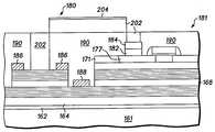
도 4는 본 발명의 다른 실시예에 따른 장치 구조(50)의 단면을 개략적으로 도시한다. 장치 구조(50)는 단결정 반도체 기판(52), 바람직하게 단결정 실리콘 웨이퍼를 포함한다. 단결정 반도체 기판(52)은 두 개의 지역(53 및 54)을 포함한다. 점선(56)으로 도시된 전기적 반도체 구성요소는 지역(53)에 형성된다. 전기 구성요소(56)는 레지스터, 캐패시터, 다이오드 또는 트랜지스터 같은 액티브 반도체 구성요소 또는 CMOS 집적 회로 같은 집적 회로이다. 예를 들어, 전기적 반도체 구성요소(56)는 실리콘 집적 회로가 잘 배치된 디지털 신호 공정 또는 다른 기능을 수행하기 위하여 구성된 CMOS 집적 회로일 수 있다. 지역(53)에서 전기적 반도체 구성요소는 반도체 산업에서 잘 알려져 있고 폭넓게 사용된 통상의 반도체 공정에 의해 수행된다. 실리콘 디산화물 등 같은 절연 재료(58)의 층은 전기적 반도체 구성요소(56)상에 놓인다.4 schematically shows a cross section of a
지역(53)에서 반도체 구성요소(56)의 공정 동안 형성되거나 증착된 절연 재료(58) 및 어떤 다른 층은 상기 지역에서 베어 실리콘 표면을 제공하기 위하여 지역(54)의 표면으로부터 제거된다. 잘 알려진 바와 같이, 베어 실리콘 표면은 고반응성이고 네이티브 실리콘 산화물 층은 베어 표면상에 빠르게 형성될 수 있다. 바륨 또는 바륨 및 산소의 층은 지역(54)의 표면상 네이티브 산화물 층위에 증착되고 제 1 템플레이트 층(도시되지 않음)을 형성하기 위하여 산화된 표면과 반응된다. 본 발명의 일 실시예에 따라, 단결정 산화물 층(60)은 분자 빔 에피텍시의 공정에 의해 템플레이트 층위에 형성된다. 바륨, 티타늄 및 산소를 포함하는 반응제는 단결정 산화물 층을 형성하기 위하여 템플레이트 층위에 증착된다. 증착동안 산소의 부분 압력은 단결정 바륨 티타네이트 층(60)을 형성하기 위하여 바륨 및 티타늄과 완전히 반응하기에 필요한 최소치 근처에서 유지된다. 산소의 부분 압력은 산소의 과압력을 제공하고 산소가 성장된 단결정 산화물 층을 통하여 확산되도록 증가된다. 바륨 티타네이트를 통한 산소 확산은 제 2 지역상 실리콘 산화물의 비정질 층(62)을 형성하기 지역(54)의 표면 및 실리콘 기판과 단결정 산화물 사이의 인터페이스에서 실리콘과 반응을 유발한다.
본 발명의 실시에에 따라, 단결정 산화물 층(60)의 증착 단계는 티타늄, 바륨, 바륨 및 산소, 또는 티타늄 및 산소의 1-10 단층들일 수 있는 제 2 템플레이트 층(64)을 증착함으로써 종결된다. 그 다음 단결정 화합물 반도체 재료의 층(66)은 분자 빔 에피텍시의 공정에 의해 제 2 템플레이트 층 위에 증착된다. 층(66)의 증착은 비소층을 템플레이트에 증착함으로써 시작된다. 이 초기 단계는 단결정 갈륨 비소화물을 형성하기 위하여 갈륨 및 비소를 증착함으로써 행해진다. 선택적으로, 스트론튬은 상기 실시예에서 바륨을 대체한다.According to the practice of the present invention, the step of depositing the single
본 발명의 다른 실시예에 따라, 저먼(68)으로 도시된 반도체 구성요소는 화합물 반도체 층(66)에 형성된다. 반도체 구성요소(68)는 갈륨 비소화물 또는 다른 Ⅲ-Ⅴ 화합물 반도체 재료 장치의 제조 시 사용된 공정 단계에 의해 형성될 수 있다. 반도체 구성요소(68)는 어떤 액티브 또는 패시브 구성요소이고, 바람직하게 화합물 반도체 재료의 물리적 특성의 장점을 사용하고 취하는 반도체 레이저, 광 방사 다이오드, 광검출기, 헤테로접합 바이폴라 트랜지스터(HBT), 고주파수 MESFET, 또는 다른 구성요소이다. 점선(70)으로 도시된 금속 도전체는 장치(68) 및 장치(56)를 전기적으로 결합하기 위하여 형성되고, 실리콘 기판에 형성된 적어도 하나의 구성요소 및 단결정 화합물 반도체 재료층에 형성된 하나의 장치를 포함하는 집적 장치를 실행시킨다. 비록 도시된 구조(50)가 실리콘 기판(52)상에 형성된 구조로서 기술되고 바륨(스트론튬) 티타네이트 층(60) 및 갈륨 비소화물 층(66)을 가지지만, 유사한 장치는 이 명세서에 기술된 다른 기판, 단결정 산화물 층 및 다른 화합물 반도체 층을 사용하여 제조된다.In accordance with another embodiment of the present invention, the semiconductor component shown as German 68 is formed in
도 5는 본 발명의 다른 실시예에 따른 반도체 구조(72)를 도시한다. 구조(72)는 지역(75) 및 지역(76)을 포함하는 단결정 실리콘 웨이퍼 같은 단결정 반도체 기판(74)을 포함한다. 점선(78)으로 도시된 전기 구성요소 는 반도체 산업에서 일반적으로 사용되는 통상적인 실리콘 장치 공정 기술을 사용하여 지역(75)에서 형성된다. 상기된 바와 유사한 공정 단계를 사용하여, 단결정 산화물 층(80) 및 중간의 비정질 실리콘 산화물 층(82)은 기판(74)의 상부 지역(76)에 형성된다. 템플레이트 층(84) 및 추후 단결정 반도체 층(86)은 단결정 산화물 층(80)상에 형성된다. 본 발명의 다른 실시예에 따라, 부가적인 단결정 산화물 층(88)은 층(80)을 형성하기 위하여 사용된 것과 유사한 공정 단계에 의해 상부 층(86)에 형성되고, 부가의 단결정 반도체 층(90)은 층(86)을 형성하기 위하여 사용된 것과 유사한 공정 단계에 의해 단결정 산화물 층(88)상에 형성된다. 본 발명의 일 실시예에 따라, 적어도 하나의 층(86 및 90)은 화합물 반도체 재료로 형성된다.5 illustrates a
점선(92)으로 도시된 반도체 구성요소는 적어도 부분적으로 단결정 반도체 층(86)으로 형성된다. 본 발명의 일 실시예에 따라, 반도체 구성요소(92)는 단결정 산화물 층(88)에 의해 부분적으로 형성된 게이트 유전체를 가진 필드 효과 트랜지스터를 포함한다. 게다가, 단결정 반도체 층(92)은 필드 효과 트랜지스터의 게이트 전극을 실행하기 위하여 사용될 수 있다. 본 발명의 일 실시예에 따라, 단결정 반도체 층(86)은 그룹 Ⅲ-Ⅴ 화합물로 형성되고 반도체 구성요소(92)는 그룹 Ⅲ-Ⅴ 구성요소 재료의 높은 모빌리티 특성의 장점을 취하는 무선 주파수 증폭기이다. 본 발명의 다른 실시예에 따라, 점선(94)으로 도시된 전기 상호 접속부는 구성요소(78) 및 구성요소(92)를 전기적으로 상호 접속한다. 따라서 구조(72)는 두 개의 단결정 반도체 재료의 유일한 특성의 장점을 취하는 구성요소를 집적한다.The semiconductor component shown by dashed
보다 구체적인 실시예에 의해, 다른 집적 회로 및 시스템은 도 6 내지 18에 도시된다. 도 6은 신호 트랜시버 수단(101), 집적 회로(102), 출력 유니트(103), 및 입력 유니트(104)를 가지는 통신 장치(100)의 일부를 도시하는 간략화된 블록도를 포함한다. 신호 트랜시브 수단의 실시에는 안테나, AHPA, 또는 정보나 데이터가 외부 유니트로 또는 외부 유니트로부터 보내질 수 있는 어떤 다른 수단을 포함한다. 여기에 사용된 바와 같이, 트랜시브는 신호 트랜시브 수단이 통신 장치로부터 및 통신 장치로 신호를 단지 수신하거나, 단지 전송하거나, 또는 수신 및 전송할 수 있다는 것을 의미하기 위해 사용된다. 출력 유니트(103)는 디스플레이, 모니터, 스피커 등을 포함한다. 입력 유니트는 마이크로폰, 키보드 등을 포함한다. 다른 실시예에서 출력 유니트(103) 및 입력 유니트(104)는 메모리 같은 KS일 유니트에 의해 대체될 수 있다. 메모리는 하드디스크, 플래시 메모리 카드 또는 모듈 등을 포함하는 랜덤 액세스 메모리 또는 비휘발성 메모리를 포함한다.By more specific embodiment, other integrated circuits and systems are shown in FIGS. 6-18. 6 includes a simplified block diagram illustrating a portion of a
집적 회로는 연속적인 기판상에 또는 기판 내에 통합적으로 관련된 적어도 두 개의 소자들(예를 들어, 트랜지스터, 다이오드, 레지스터, 캐패시터 등)의 결합물이다. 집적 회로(102)는 화합물 반도체 부분(1022), 바이폴라 부분(1024), MOS 부분(1026)을 포함한다. 화합물 반도체 부분(1022)은 화합물 반도체 재료 내에 적 어도 부분적으로 형성된 전기 구성요소를 포함한다. 화합물 반도체 부분(1022)내의 트랜지스터 및 다른 전기 구성요소는 대략 0.8 GHz의 무선 주파수에서 신호를 처리할 수 있다. 다른 실시예에서, 신호는 보다 낮거나 높은 주파수일 수 있다. 예를 들어, 인듐 갈륨 비소화물 같은 몇몇 재료는 대략 27 GHz의 무선 주파수 신호로 신호를 처리할 수 있다.An integrated circuit is a combination of at least two elements (eg, transistors, diodes, resistors, capacitors, and the like) that are integrally associated on or within a continuous substrate.
화합물 반도체 부분(1022)은 듀플렉서(10222), 무선 주파수 대 기저대역 컨버터(10224)(디모듈레이팅 수단 또는 디모듈레이팅 회로), 기저대역 대 무선 주파수 컨버터(10226)(모듈레이팅 수단 또는 모듈레이팅 회로), 파워 증폭기(10228), 및 절연기(10229)를 더 포함한다. 바이폴라 부분(1024) 및 MOS 부분(1026)은 통상적으로 그룹 Ⅳ 반도체 재료로 형성된다. 바이폴라 부분(1024)은 수신 증폭기(10242), 아날로그 대 디지털 컨버터(10244), 디지털 대 아날로그 컨버터(10246), 및 전송 증폭기(10248)를 포함한다. MOS 부분(1026)은 디지털 신호 처리 수단(10262)을 포함한다. 상기 수단의 일례는 모토롤라 DSP 566xx(일루노이스 샤움버그의 모토롤라, 인코포레이티드) 및 텍사스 인스트루먼트 TMS 320C54x(텍사스 달라스의 텍사스 인스트루먼트)의 디지털 신호 처리기 같은 마켓에서 판매되는 DSP 코어중 어느 하나를 포함한다. 이런 디지털 신호 처리 수단(10262)은 통상적으로 상보형 MOS(CMOS) 트랜지스터 및 아날로그 대 디지털 및 디지털 대 아날로그 컨버터를 포함한다. 명확하게, 다른 전기 구성요소는 집적 회로(102)에 존재한다.
하나의 동작 모드에서, 통신 장치(100)는 신호 전송 수단(101)의 일부인 안 테나로부터 신호를 수신한다. 신호는 듀플렉서(10227)를 통하여 무선주파수 대 기저대역 컨버터(10224)로 보내진다. 아날로그 데이터 또는 다른 정보는 수신 증폭기(10224)에 의해 증폭되고 디지털 신호 처리 수단(10262)으로 전송된다. 디지털 신호 처리 수단(10262)이 정보 또는 다른 데이터를 처리한 후, 처리된 정보 또는 다른 데이터는 출력 유니트(103)로 전송된다. 만약 통신 장치가 페이저이면, 출력 유니트는 디스플레이일 수 있다. 만약 통신 장치가 셀방식 전화이면, 출력 유니트(103)는 스피커, 디스플레이 또는 양쪽을 포함할 수 있다.In one mode of operation, the
데이터 또는 다른 정보는 반대 방향으로 통신 장치(100)를 통하여 보내진다. 데이터 또는 다른 정보는 입력 유니트(104)를 통하여 온다. 셀방식 전화에서, 이것은 마이크로폰 또는 키패드를 포함한다. 정보 또는 다른 데이터는 디지털 신호 처리 수단(10262)을 사용하여 처리된다. 처리후, 신호는 디지털 대 아날로그 컨버터(10246)를 사용하여 컨버트된다. 컨버트된 신호는 전송 증폭기(10248)에 의해 증폭된다. 증폭된 신호는 기저대역 대 무선 주파수 컨버터(10226)에 의해 변조되고 전력 증폭기(10228)에 의해 추가로 증폭된다. 증폭된 RF 신호는 절연기(10229) 및 듀플렉서(10222)를 통하여 안테나로 통과한다.Data or other information is sent through the
통신 장치(100)의 종래 기술 실시예는 적어도 두 개의 분리된 집적 회로를 가진다; 하나는 화합물 반도체 부분(1022)에 관한 것이고 다른 하나는 MOS 부분(1026)에 관한 것이다. 바이폴라 부분(1024)은 MOS 부분(1026)과 동일한 집적 회로 상에 있거나 다른 집적 회로 상에 있을 수 있다. 본 발명의 실시예를 이용하여, 모두 3개의 부분이 단일 집적 회로에 형성될 수 있다. 모든 트랜지스터는 단 일 집적 회로에 제공되기 때문에, 통신 장치는 최소화되고 보다 우수한 휴대성을 허용한다.The prior art embodiment of the
현재는 도 7 내지 11에 도시된 바와 같은 집적 회로(102)의 예시적 부분을 형성하는 방법이 개시된다. 도 7에서, p 타입 도핑 단결정 실리콘 기판(110)은 화합물 반도체 부분(1022), 바이폴라 부분(1024), 및 MOS 부분(1026)을 가진다. 바이폴라 부분 내에는 단결정 실리콘 기판이 N+ 매몰 영역(1102)을 형성하기 위하여 도핑된다. 가볍게 p 타입 도핑된 에피텍셜 단결정 실리콘 층(1104)은 매몰된 지역(1102) 및 기판(110)상에 형성된다. 도핑 단계는 N+ 매몰된 지역(1102)상 가볍게 n 타입 도핑된 드리프트 지역(1117)을 형성하기 위하여 수행된다. 도핑 단계는 바이폴라 지역(1024)의 섹션 내 가벼운 p 타입 에피텍셜층의 도판트 타입을 가벼운 n 타입 단결정 실리콘 지역으로 전환한다. 필드 절연 지역(1106)은 바이폴라 부분(1024) 및 MOS 부분(1026) 사이에 형성된다. 게이트 유전층(1110)은 MOS 부분(1026)내 에피텍셜층(1104)의 일부 상에 형성되고, 게이트 전극(1112)은 게이트 유전층(1110)상에 형성된다. 측벽 스페이서(1115)는 게이트 전극(1112) 및 게이트 유전층(1110)의 수직 측면을 따라 형성된다.At present, a method of forming an exemplary portion of
p 타입 도판트는 액티브 또는 진성 베이스 지역(1114)을 형성하기 위하여 드리프트 지역(1117)으로 유도된다. n 타입, 깊은 컬렉터 지역(1108)은 바이폴라 부분(1024)에 형성되어 매몰된 지역(1102)에 대한 전기 접속이 이루어진다. 선택적인 n 타입 도핑은 N+ 도핑 지역(1116) 및 에미터 지역(1120)을 형성하기 위하여 수 행된다. N+ 도핑 지역(1116)은 게이트 전극(1112)의 인접 측면을 따라 층(1104)내에 형성되고 MOS 트랜지스터에 대한 소스, 드레인, 또는 소스/드레인 지역이다. N+ 도핑 지역(1116) 및 에미터 지역(1120)은 입방 센티미터당 적어도 1E19 원자의 도핑 농도를 가져서 오움 접촉이 형성된다. p 타입 도핑 지역은 P+도핑 지역(입방 센티미터당 적어도 1E19 원자의 도핑 농도)인 인액티브 또는 외부 베이스 지역(1118)을 형성하기 위하여 형성된다.P type dopant is directed to drift
상기된 실시예에서, 몇몇 공정 단계는 수행되지만 웰 지역 형성, 임계치 조절 주입, 채널 펀치스로우 방지 주입, 필드 펀치스로우 방지 주입, 다양한 마스킹 층 같은 것은 도시되거나 추가로 기술되지 않는다. 상기 공정시 이런 지점까지 장치의 형성은 통상적인 단계를 사용하여 수행된다. 도시된 바와 같이, 표준 N 채널 MOS 트랜지스터는 MOS 지역(1026)내에 형성되고, 수직 NPN 바이폴라 트랜지스터는 바이폴라 부분(1024)내에 형성된다. 이런 점에서, 화합물 반도체 부분(1022)내에 형성된 회로는 없다.In the embodiments described above, some process steps are performed but well region formation, threshold controlled implants, channel punch throw prevention implants, field punch throw prevention implants, and various masking layers are not shown or further described. Formation of the device up to this point in the process is carried out using conventional steps. As shown, a standard N-channel MOS transistor is formed in
집적회로의 바이폴라 및 MOS 부분을 공정하는 동안 형성된 모든 층은 화합물 반도체 부분(1022)의 표면으로부터 제거된다. 베어 실리콘 표면은 상기된 방식으로 이 부분의 추후 공정 동안 제공된다.All layers formed during the processing of the bipolar and MOS portions of the integrated circuit are removed from the surface of the
수용 버퍼층(124)은 도 8에 도시된 기판(110)상에 형성된다. 버퍼층은 부분(1022)에서 적당하게 제공된(즉, 적당한 템플레이트 층을 가짐) 베어 실리콘 표면상 단결정 층으로서 형성될 것이다. 그러나 부분(1024 및 1026)상에 형성된 층(124)의 부분은 다결정 또는 비정질인데, 그 이유는 상기 부분은 단결정이 아닌 재료 상에 형성되어 단결정 성장을 할 수 없기 때문이다. 버퍼층(124)은 통상적으로 단결정 금속 산화물 또는 질화물 층이고 대략 2 내지 100 나노미터 범위의 두께를 가진다. 하나의 특정 실시예에서, 버퍼층은 대략 5 내지 15nm 두께이다. 버퍼층의 형성동안, 비정질 중간층(122)은 집적 회로(102)의 최상부 실리콘 표면을 따라 형성된다. 이 비정질 중간층(122)은 실리콘 산화물을 포함하고 대략 1 내지 5 nm의 범위 및 두께를 가진다. 특정 실시예에서, 두께는 대략 2nm이다. 버퍼층(124) 및 비정질 중간층(122)의 형성 다음, 템플레이트 층(126)은 형성되고 1 내지 10 단층 재료 범위의 두께를 가진다. 특정 실시예에서, 재료는 도 1 내지 5에 관하여 기술된 바와 같은 티타늄 비소, 스트론튬 산소 비소, 또는 다른 유사한 재료를 포함한다.The receiving
단결정 화합물 반도체 층(132)은 도 9에 도시된 바와 같이 버퍼층(124)의 단결정 부분 위에 에피텍셜적으로 성장된다. 단결정이 아닌 층(124)의 부분 상에 성장된 층(132)의 부분은 다결정 또는 비정질이다. 단결정 화합물 반도체 층은 다수의 방법에 의해 형성되고 상기된 갈륨 비소화물, 알루미늄 갈륨 비소화물, 인듐 인, 또는 다른 화합물 반도체 재료 같은 재료를 포함한다. 층의 두께는 대략 1 내지 5,000 nm의 범위이고, 바람직하게 100 내지 500 nm이다. 특정 실시예에서, 각각의 템플레이트 층 내의 원소는 수용 버퍼층(124), 단결정 화합물 반도체 재료(132)에 존재하거나, 양쪽에 존재한다. 그러므로, 템플레이트 층(126)과 그것의 인접한 층 사이의 기술은 공정 동안 나타나지 않는다. 그러므로, 전송 전자 현미경(TEM) 포토그래프가 얻어지고, 버퍼층(124)과 단결정 화합물 반도체 층(132) 사이의 인터페이스가 도시된다.The single crystal
이 시점에서, 화합물 반도체 층(132)과 버퍼층(124)의 섹션은 도 10에 도시된 바와 같이 바이폴라 부분(1024) 및 MOS 부분(1026) 윗부분으로부터 제거된다. 섹션이 제거된 후, 절연층(142)은 기판(110)상에 형성된다. 절연층(142)은 산화물, 질화물, 산화질화물, 낮은 k 유전체 등 같은 다수의 재료를 포함할 수 있다. 여기에 사용된 바와 같이, 낮은 k는 대략 3.5 보다 낮은 유전상수를 가진 재료이다. 절연층(142)이 증착된 후, 폴리싱되고, 단결정 화합물 반도체 층(132) 위에 놓이는 절연층(142)의 부분을 제거한다.At this point, sections of
트랜지스터(144)는 단결정 화합물 반도체 부분(1022)내에 형성된다. 게이트 전극(148)은 단결정 화합물 반도체 층(132)상에 형성된다. 도핑된 지역(146)은 단결정 화합물 반도체 층(132)내에 형성된다. 이 실시에에서, 트랜지스터(144)는 금속 반도체 필드 효과 트랜지스터(MESFET)이다. 만약 MESFET가 n 타입 MESFET이면, 도핑된 지역(146) 및 단결정 화합물 반도체 층(132)은 n 타입 도핑된다. 만약 p 타입 MESFET가 형성되면, 도핑된 지역(146) 및 단결정 화합물 반도체 층(132)은 반대 도핑 타입을 가진다. 보다 무겁게 도핑된(N+) 지역(146)은 오움 접촉이 단결정 화합물 반도체 층(132)에 이루어지게 한다. 이 시점에서, 집적 회로내의 액티브 장치는 형성된다. 이런 특정 실시예는 n 타입 MESFET, 수직 NPN 바이폴라 트랜지스터, 및 평면형 n 채널 MOS 트랜지스터를 포함한다. P 채널 MOS 트랜지스터, P 타 입 수직 바이폴라 트랜지스터, P 타입 MESFET 및 수직 및 평면형 트랜지스터의 결합물을 포함하는 많은 다른 타입의 트랜지스터는 사용될 수 있다. 또한, 레지스터, 캐패시터, 다이오드 등 같은 다른 전기 구성요소는 하나 이상의 부분(1022, 1024 및 1026)으로 형성된다.
공정은 도 11에 도시된 바와 같이 실질적으로 완성된 집적 회로(102)를 계속 형성한다. 절연층(152)은 기판(110)상에 형성된다. 절연층(152)은 도 11에 도시되지 않은 에칭 스톱 또는 폴리싱 스톱 지역을 포함한다. 제 2 절연층(154)은 제 1 절연층(152)상에 형성된다. 층(154, 152, 142, 124 및 122) 부분은 장치가 상호 접속되는 접촉 개구부를 형성하기 위하여 제거된다. 상호접속 트렌치는 접촉부 사이에 측면 접속부를 제공하기 위하여 절연층(154)내에 형성된다. 도 11에 도시된 바와 같이, 상호접속(1562)는 부분(1022)내의 n 타입 MESFET의 소스 또는 드레인 지역을 바이폴라 부분(1024)내의 NPN 트랜지스터의 깊은 컬렉터 지역(1108)에 접속시킨다. NPN 트랜지스터의 이미터 지역(1120)은 MOS 부분(1026)내의 n 채널 MOS 트랜지스터의 도핑된 지역(1116)중 하나에 접속된다. 다른 도핑된 지역(1116)은 도시되지 않은 집적 회로의 다른 부분에 전기적으로 접속된다.The process continues to form the substantially completed
패시베이션 층(156)은 상호접속(1562, 1564 및 1566) 및 절연층(154)상에 형성된다. 다른 전기 접속은 도시된 트랜지스터뿐 아니라 집적 회로(102)내의 다른 전기 또는 전자 구성요소에서 이루어지고 이는 도면에 도시되지 않는다. 게다가, 부가적인 절연층 및 상호접속은 집적 회로(102)내의 다양한 구성요소 사이에 적당한 상호접속을 형성하기 위하여 필요하면 형성된다.
이전 실시예에 도시된 바와 같이, 양쪽 화합물 반도체 및 그룹 Ⅳ 반도체 재료 양쪽에 대한 액티브 장치는 단일 집적 회로에 집적될 수 있다. 동일한 집적 회로 내에 바이폴라 트랜지스터 및 MOS 트랜지스터 양쪽을 통합하는데 어려움이 있기 때문에, 바이폴라 부분내의 구성요소의 몇몇을 화합물 반도체 부분(1022) 또는 MOS 부분(1024)으로 이동하는 것이 가능하다. 특히, 도 6에 대해 설명된 실시예를 참조하여, 증폭기(10248 및 10242)는 화합물 반도체 부분(1022)으로 이동되고, 컨버터(10244 및 10246)는 MOS 부분(1026)으로 이동될 수 있다. 그러므로, 바이폴라 트랜지스터를 제조하는데만 사용된 특정 제조 단계는 제거될 수 있다. 그러므로, 집적 회로에 화합물 반도체 부분 및 MOS 부분만이 있을 수 있다.As shown in the previous embodiment, active devices for both compound semiconductors and group IV semiconductor materials can be integrated into a single integrated circuit. Because of the difficulty in integrating both bipolar transistors and MOS transistors within the same integrated circuit, it is possible to move some of the components in the bipolar portion to the
다른 실시예에서, 집적 회로는 동일한 집적 회로의 그룹 Ⅳ 반도체 지역 내 MOS 트랜지스터에 화합물 반도체 부분 및 광학 상호접속(도파관)내의 광학 레이저를 포함하도록 형성될 수 있다. 도 12 내지 18은 일 실시예를 도시한다.In another embodiment, the integrated circuit may be formed to include a compound semiconductor portion and an optical laser in an optical interconnect (waveguide) in a MOS transistor in a Group IV semiconductor region of the same integrated circuit. 12-18 illustrate one embodiment.
도 12는 단결정 실리콘 웨이퍼(161)을 포함하는 집적 회로(160) 부분의 단면을 도시한다. 이전에 기술된 것과 유사하게 비정질 중간층(162) 및 버퍼층(164)은 웨이퍼(161)상에 형성된다. 이 특정 실시예에서, 광학 레이저를 형성하기 위하여 필요한 층은 우선 형성되고 MOS 트랜지스터를 위해 필요한 층이 형성된다. 도 12에서, 하부 미러 층(166)은 화합물 반도체 재료의 교번 층을 포함한다. 예를 들어, 광학 레이저내의 제 1, 제 3 및 제 5 막은 갈륨 비소화물같은 재료를 포함할 수 있고, 하부 미러 층(166)내의 제 2, 제 4 및 제 6 막은 알루미늄 갈륨 비소화물 또는 그 반대를 포함할 수 있다. 층(168)은 광자 생성을 위해 사용될 액티브 지역을 포함한다. 상부 미러 층(170)은 하부 미러층(166)과 유사한 방식으로 형성되고 화합물 반도체 재료의 교번 막을 포함한다. 하나의 특정 실시예에서, 상부 미러층(170)은 p 타입 도핑 화합물 반도체 재료이고, 하부 미러층(166)은 n 타입 화합물 반도체 재료이다.12 shows a cross section of an
버퍼층(164)과 유사한 다른 수용 버퍼층(172)은 상부 미러층(170)상에 형성된다. 다른 실시예에서, 버퍼층(164 및 172)은 다른 재료를 포함할 수 있다. 그러나, 그 기능은 각각이 화합물 반도체 층 및 단결정 그룹 Ⅳ반도체 층 사이 전이를 형성하는데 사용되는 것과 동일하다. 단결정 그룹 Ⅳ반도체 층(174)은 버퍼층(172)상에 형성된다. 하나의 특정 실시예에서, 단결정 그룹 Ⅳ 반도체 층(174)은 갈륨, 실리콘 게르마늄, 실리콘 게르마늄 카바이드 등을 포함한다.Another receiving
도 13에서, MOS 부분은 상부 단결정 그룹 Ⅳ반도체 층(174)내에 전기 부품을 형성하기 위하여 공정된다. 도 13에 도시된 바와 같이, 필드 절연 지역(171)은 층(174)의 부분으로 형성된다. 게이트 유전층(173)은 층(174)상에 형성되고, 게이트 전극(175)은 게이트 유전층(173)상에 형성된다. 도핑된 지역(177)은 도시된 바와 같이 트랜지스터(181)에 대한 소스, 드레인, 또는 소스/드레인 영역이다. 측벽 스페이서(179)는 게이트 전극(175)의 수직 측면에 인접하게 형성된다. 다른 구성요소는 적어도 일부의 층(174)내에 만들어진다. 이들 구성요소는 다른 트랜지스터(n 채널 또는 p 채널), 캐패시터, 트랜지스터, 다이오드 등을 포함한다.In FIG. 13, the MOS portion is processed to form an electrical component in the upper single crystal group
단결정 그룹 Ⅳ반도체 층은 도핑된 지역(177)의 하나 상에서 에피텍셜적으로 성장된다. 상부 부분(184)은 P+ 도핑되고, 하부 부분(182)은 도 13에 도시된 바와 같이 실질적으로 진성(도핑되지 않음)으로 남는다. 상기 층은 선택적 에피텍셜 공정을 사용하여 형성된다. 일 실시예에서, 절연층(도시되지 않음)은 트랜지스터(181) 및 필드 절연 지역(171)상에 형성된다. 절연층은 도핑된 지역(177)중 하나를 노출시키기 위한 개구부를 형성하기 위하여 패턴화된다. 처음에, 선택적인 에피텍셜층은 도판트없이 형성된다. 전체 선택적인 에피텍셜층은 진성이거나, p 타입 도판트는 선택적인 에피텍셜층의 형성 마지막에 부가될 수 있다. 만약 선택적인 에피텍셜층이 형성된 바와 같이 진성이면, 도핑 단계는 주입 또는 노 도핑에 의해 형성될 수 있다. P+ 상부 부분(184)이 어떻게 형성되는지에 관계없이, 절연층은 도 13에 도시된 최종 구조를 형성하기 위하여 제거된다.The single crystal group IV semiconductor layer is epitaxially grown on one of the doped
다음 단계는 도 14에 도시된 바와 같이 광학 레이저(180)를 한정하기 위하여 수행된다. 필드 절연 영역(171) 및 버퍼층(172)은 집적 회로의 화합물 반도체 부분 상에서 제거된다. 부가적인 단계는 광학 레이저(180)의 상부 미러층(170) 및 액티브 층(168)을 형성하기 위하여 수행된다. 상부 미러층(170) 및 액티브 층(168)의 측면은 실질적으로 경계를 이룬다.The next step is performed to define the
접촉부(186 및 188)는 도 14에 도시된 바와 같이 상부 미러층(170) 및 하부 미러층(166)에 대한 전기 접촉을 형성하기 위하여 형성된다. 접촉부(186)는 광(광자)이 상부 미러층(170)을 통하여 추후에 형성되는 광학 도파관으로 통과하도록 환형 모양을 가진다.
절연층(190)은 도 15에 도시된 바와 같이 접촉 층(186) 및 도핑된 지역(177)중 하나로 연장하는 광학 개구부를 형성하기 위하여 패턴화된다. 절연 재료는 산화물, 질화물, 산화질화물, 낮은 k 유전체, 또는 어떤 상기 화합물의 결합물을 포함하는 어떤 수의 다른 재료이다. 개구부(192)를 형성한 후, 보다 높은 굴절률 재료(202)는 도 16에 도시된 바와 같이 절연층(190)상에 층을 증착하고 그것을 충전하기 위하여 개구부내에 형성된다. 보다 높은 굴절률 재료(202)와 관련하여, "보다 높은(higher)"은 절연층(190)(즉, 재료 202가 절연층 190에 비해 높은 굴절률을 가짐)의 재료와 관련된다. 선택적으로, 비교적 얇은 낮은 굴절률 막(도시되지 않음)은 보다 높은 굴절률 재료(202)를 형성하기 전에 형성된다. 하드 마스크 층(204)은 높은 굴절률 층(202)상에 형성된다. 하드 마스크 층(204)의 부분, 및 높은 굴절률 층(202)은 개구부상에 높이는 부분으로부터 제거되고 도 16의 측면에 더욱 밀접한 영역으로 제거된다.Insulating
광학 상호접속인 광학 도파관의 형성 밸런스는 도 17에서 도시된 바와 같이 완성된다. 증착 과정(가능하게 깊은 에칭 과정)은 측벽 섹션(212)을 효과적으로 형성하도록 수행된다. 이 실시예에서, 측벽 섹션(212)은 재료(202)와 동일한 재료로 만들어진다. 하드 마스크 층(204)은 그 다음 제거되고 낮은 굴절률 층(214)(매체 202 및 층 212에 비해 낮은)은 보다 높은 굴절률 재료(212 및 202) 및 절연층(190)의 노출 부분 상에 형성된다. 도 17의 점선은 높은 굴절률 재료들(202 및 212) 사이의 보더를 도시한다. 이런 표시는 동일한 재료로 만들어지지만 다른 시간에 형성되는 것을 식별하기 위하여 사용된다.The formation balance of the optical waveguide that is the optical interconnection is completed as shown in FIG. The deposition process (possibly deep etching process) is performed to effectively form the
공정은 도 18에 도시된 바와 같이 실질적으로 완성된 집적 회로를 형성하기 위하여 계속된다. 패시베이션 층(220)은 광학 레이저(180) 및 MOSFET 트랜지스터(181)상에 형성된다. 비록 도시되지는 않았지만, 다른 전기 또는 광학 접속부가 집적 회로내의 구성요소에 만들어지지만 도 18에 도시되지는 않는다. 이들 상호접속은 다른 광학 도파관이거나 금속 상호접속을 포함할 수 있다.The process continues to form a substantially completed integrated circuit as shown in FIG.
다른 실시예에서, 다른 타입의 레이저는 형성된다. 예를 들어, 다른 타입의 레이저는 수직 대신 수평으로 광(광자)을 방사할 수 있다. 만약 광이 수평으로 방사되면, MOSFET 트랜지스터는 기판(161)내에 형성될 수 있고, 광학 도파관은 재구성되어, 레이저는 트랜지스터에 적당하게 결합된다(광학적으로 접속된다). 특정 실시예에서, 광학 도파관은 버퍼층의 적어도 일부를 포함한다. 다른 구성은 가능하다.In other embodiments, other types of lasers are formed. For example, other types of lasers can emit light (photons) horizontally instead of vertically. If the light is emitted horizontally, the MOSFET transistors can be formed in the
명확히, 화합물 반도체 부분 및 그룹 Ⅳ 반도체 부분을 가진 집적 회로의 이들 실시예는 본 발명의 실시예를 도시하기 위한 것이고, 본 발명을 제한하지는 않는다. 본 발명의 다른 결합물 및 다른 실시예가 다수 있다. 예를 들어, 화합물 반도체 부분은 광 방사 다이오드, 광검출기, 다이오드 등을 포함하고, 그룹 Ⅳ 반도체는 통상적인 MOS 집적 회로에 형성될 수 있는 디지털 논리, 메모리 어레이, 및 대부분의 구조를 포함할 수 있다. 본 발명의 실시예를 사용함으로써, 그룹 Ⅳ 반도체 재료에서 보다 잘 작동하는 다른 구성요소를 가진 화합물 반도체 재료에서 보다 잘 작동하는 장치를 집적하기가 보다 간단하다. 이것은 장치가 줄어들게 하고, 제조 비용이 감소되며, 수율 및 신뢰성이 증가되게 한다.Clearly, these embodiments of integrated circuits having compound semiconductor portions and group IV semiconductor portions are intended to illustrate embodiments of the invention and do not limit the invention. There are many other combinations and other embodiments of the invention. For example, the compound semiconductor portion may include light emitting diodes, photodetectors, diodes, and the like, and group IV semiconductors may include digital logic, memory arrays, and most structures that may be formed in conventional MOS integrated circuits. . By using embodiments of the present invention, it is simpler to integrate devices that work better in compound semiconductor materials with other components that work better in group IV semiconductor materials. This results in fewer devices, reduced manufacturing costs, and increased yields and reliability.
비록 도시되지는 않았지만, 단결정 그룹 Ⅳ 웨이퍼는 웨이퍼 상 화합물 반도체 전기 구성요소만을 형성하는데 사용된다. 이 방식에서, 웨이퍼는 웨이퍼 위에 놓인 단결정 화합물 반도체 층 내에 화합물 반도체 전기 구성요소의 제조 동안 사용된 "핸들(handle)" 웨이퍼이다. 그러므로, 전기 구성요소는 대략 200 밀리미터의 직경 및 가능하게 적어도 대략 300 밀리미터의 직경을 가진 웨이퍼상 Ⅲ-Ⅴ 또는 Ⅱ-Ⅵ 반도체 재료 내에 형성될 수 있다.Although not shown, single crystal group IV wafers are used to form only compound semiconductor electrical components on the wafer. In this manner, the wafer is a "handle" wafer used during the fabrication of compound semiconductor electrical components in a single crystal compound semiconductor layer overlying the wafer. Therefore, the electrical component can be formed in a III-V or II-VI semiconductor material on a wafer having a diameter of approximately 200 millimeters and possibly a diameter of at least approximately 300 millimeters.
이런 타입의 기판 사용에 의해, 비교적 값싼 "핸들" 웨이퍼가 비교적 보다 내구성이 있고 베이스 재료를 제조하기 쉬운 것들을 위에 배치함으로써 화합물 반도체 웨이퍼의 연약한 성질을 극복한다. 그러므로, 비록 기판 자체가 그룹 Ⅳ 반도체 재료를 포함하지 않을지라도 모든 전기 구성요소, 특히 모든 액티브 전자 장치가 화합물 반도체 재료 내에 형성될 수 있도록 형성될 수 있다. 화합물 반도체 장치에 대한 제조 비용은 보다 큰 기판이 비교적 작고 보다 연약한 종래 화합물 반도체 웨이퍼와 비교하여 보다 경제적이고 쉽게 공정될 수 있기 때문에 감소한다.By using this type of substrate, relatively inexpensive "handle" wafers overcome the fragile properties of compound semiconductor wafers by placing on top of those that are relatively more durable and easier to manufacture base materials. Therefore, even if the substrate itself does not contain a group IV semiconductor material, all electrical components, in particular all active electronic devices, can be formed so that they can be formed in the compound semiconductor material. The manufacturing cost for compound semiconductor devices is reduced because larger substrates can be more economically and easily processed compared to conventional compound semiconductor wafers that are relatively small and softer.
상기 설명에서, 본 발명은 특정 실시예를 참조하여 설명되었다. 그러나, 당업자는 다양한 변형 및 변화가 이하 청구범위에서 설명될 바와 같이 본 발명의 범위로부터 벗어나지 않고 이루어질 수 있다는 것을 이해할 것이다. 따라서, 명세서 및 도면은 제한적인 것보다 도시적인 것으로 간주되고, 모든 변형은 본 발명의 범위 내에 포함되도록 의도된다.In the foregoing description, the invention has been described with reference to specific embodiments. However, one of ordinary skill in the art appreciates that various modifications and changes can be made without departing from the scope of the present invention as set forth in the claims below. Accordingly, the specification and figures are to be regarded in an illustrative rather than a restrictive sense, and all such modifications are intended to be included within the scope of present invention.
이익, 다른 장점, 및 문제에 대한 해결책은 특정 실시예를 참조하여 이상에서 기술되었다. 그러나, 이익, 장점, 문제 해결책, 및 보다 많은 어떤 이익, 장점 또는 해결책을 유발할 수 있는 어떤 요소는 모든 청구항에 기술된다. 여기에 사용된 용어 "포함(comprising)", 또는 그것의 변형은 비배타적인 포함을 커버하기 위한 것이므로, 요소 리스트를 포함하는 공정, 방법, 아티클, 또는 장치는 이들 요소만을 포함하는 것이 아니라 상기 공정, 방법, 아티클 또는 장치에 리스트되지 않은 다른 요소를 포함할 수 있다.Benefits, other advantages, and solutions to problems have been described above with reference to specific embodiments. However, any benefit, advantage, problem solution, and any element that may give rise to any more benefit, advantage or solution are described in all claims. The term "comprising", or variations thereof, as used herein is intended to cover non-exclusive inclusions, so that a process, method, article, or apparatus that includes an element list does not include only these elements, but rather the above process. , Methods, articles, or other elements not listed in the device.
Claims (48)
Translated fromKoreanApplications Claiming Priority (2)
| Application Number | Priority Date | Filing Date | Title |
|---|---|---|---|
| US09/502,023US6392257B1 (en) | 2000-02-10 | 2000-02-10 | Semiconductor structure, semiconductor device, communicating device, integrated circuit, and process for fabricating the same |
| US09/502,023 | 2000-02-10 |
Publications (2)
| Publication Number | Publication Date |
|---|---|
| KR20020091089A KR20020091089A (en) | 2002-12-05 |
| KR100695662B1true KR100695662B1 (en) | 2007-03-19 |
Family
ID=23995993
Family Applications (5)
| Application Number | Title | Priority Date | Filing Date |
|---|---|---|---|
| KR1020027010316AExpired - LifetimeKR100695662B1 (en) | 2000-02-10 | 2001-02-08 | Process for Forming Semiconductor Structure |
| KR1020027010314AWithdrawnKR20020086514A (en) | 2000-02-10 | 2001-02-08 | Semiconductor structure |
| KR1020027010317AWithdrawnKR20020075403A (en) | 2000-02-10 | 2001-02-08 | Communicating device |
| KR1020027010310AWithdrawnKR20020077907A (en) | 2000-02-10 | 2001-02-08 | Semiconductor devices |
| KR1020027010309AWithdrawnKR20020077678A (en) | 2000-02-10 | 2001-02-08 | Semiconductor structure |
Family Applications After (4)
| Application Number | Title | Priority Date | Filing Date |
|---|---|---|---|
| KR1020027010314AWithdrawnKR20020086514A (en) | 2000-02-10 | 2001-02-08 | Semiconductor structure |
| KR1020027010317AWithdrawnKR20020075403A (en) | 2000-02-10 | 2001-02-08 | Communicating device |
| KR1020027010310AWithdrawnKR20020077907A (en) | 2000-02-10 | 2001-02-08 | Semiconductor devices |
| KR1020027010309AWithdrawnKR20020077678A (en) | 2000-02-10 | 2001-02-08 | Semiconductor structure |
Country Status (9)
| Country | Link |
|---|---|
| US (9) | US6392257B1 (en) |
| EP (5) | EP1258030A1 (en) |
| JP (5) | JP2003523084A (en) |
| KR (5) | KR100695662B1 (en) |
| CN (5) | CN1398423A (en) |
| AU (7) | AU2001234999A1 (en) |
| CA (2) | CA2399394A1 (en) |
| TW (6) | TW487969B (en) |
| WO (7) | WO2001059835A1 (en) |
Families Citing this family (159)
| Publication number | Priority date | Publication date | Assignee | Title |
|---|---|---|---|---|
| DE19942692B4 (en)* | 1999-09-07 | 2007-04-12 | Infineon Technologies Ag | Optoelectronic microelectronic assembly |
| US6392257B1 (en) | 2000-02-10 | 2002-05-21 | Motorola Inc. | Semiconductor structure, semiconductor device, communicating device, integrated circuit, and process for fabricating the same |
| US6693033B2 (en)* | 2000-02-10 | 2004-02-17 | Motorola, Inc. | Method of removing an amorphous oxide from a monocrystalline surface |
| JP2004503920A (en) | 2000-05-31 | 2004-02-05 | モトローラ・インコーポレイテッド | Semiconductor device and method of manufacturing the semiconductor device |
| US20020030246A1 (en)* | 2000-06-28 | 2002-03-14 | Motorola, Inc. | Structure and method for fabricating semiconductor structures and devices not lattice matched to the substrate |
| AU2001264987A1 (en)* | 2000-06-30 | 2002-01-14 | Motorola, Inc., A Corporation Of The State Of Delware | Hybrid semiconductor structure and device |
| WO2002009187A2 (en) | 2000-07-24 | 2002-01-31 | Motorola, Inc. | Heterojunction tunneling diodes and process for fabricating same |
| US6555946B1 (en) | 2000-07-24 | 2003-04-29 | Motorola, Inc. | Acoustic wave device and process for forming the same |
| US6590236B1 (en)* | 2000-07-24 | 2003-07-08 | Motorola, Inc. | Semiconductor structure for use with high-frequency signals |
| WO2002009148A2 (en)* | 2000-07-24 | 2002-01-31 | Motorola, Inc. | Integrated radiation emitting system and process for fabricating same |
| DE60124766T2 (en)* | 2000-08-04 | 2007-10-11 | Amberwave Systems Corp. | SILICON WAIST WITH MONOLITHIC OPTOELECTRONIC COMPONENTS |
| US7273657B2 (en)* | 2000-08-08 | 2007-09-25 | Translucent Photonics, Inc. | Rare earth-oxides, rare earth-nitrides, rare earth-phosphides and ternary alloys with silicon |
| US6638838B1 (en) | 2000-10-02 | 2003-10-28 | Motorola, Inc. | Semiconductor structure including a partially annealed layer and method of forming the same |
| WO2002033385A2 (en)* | 2000-10-19 | 2002-04-25 | Motorola, Inc. | Biochip excitation and analysis structure |
| US7065124B2 (en)* | 2000-11-28 | 2006-06-20 | Finlsar Corporation | Electron affinity engineered VCSELs |
| US6905900B1 (en) | 2000-11-28 | 2005-06-14 | Finisar Corporation | Versatile method and system for single mode VCSELs |
| US6563118B2 (en)* | 2000-12-08 | 2003-05-13 | Motorola, Inc. | Pyroelectric device on a monocrystalline semiconductor substrate and process for fabricating same |
| US20020096683A1 (en) | 2001-01-19 | 2002-07-25 | Motorola, Inc. | Structure and method for fabricating GaN devices utilizing the formation of a compliant substrate |
| US6589335B2 (en)* | 2001-02-08 | 2003-07-08 | Amberwave Systems Corporation | Relaxed InxGa1-xAs layers integrated with Si |
| US6673646B2 (en) | 2001-02-28 | 2004-01-06 | Motorola, Inc. | Growth of compound semiconductor structures on patterned oxide films and process for fabricating same |
| US20020140012A1 (en)* | 2001-03-30 | 2002-10-03 | Motorola, Inc. | Semiconductor structures and devices for detecting far-infrared light and methods for fabricating same |
| WO2002082551A1 (en) | 2001-04-02 | 2002-10-17 | Motorola, Inc. | A semiconductor structure exhibiting reduced leakage current |
| US6594409B2 (en)* | 2001-04-18 | 2003-07-15 | Apic Corporation | WDM transmitter or receiver including an array waveguide grating and active optical elements |
| US20020163010A1 (en)* | 2001-05-04 | 2002-11-07 | Motorola, Inc. | Wide bandgap semiconductor structure, semiconductor device including the structure, and methods of forming the structure and device |
| US20020175347A1 (en)* | 2001-05-22 | 2002-11-28 | Motorola, Inc. | Hybrid semiconductor input/output structure |
| US20020179957A1 (en)* | 2001-05-29 | 2002-12-05 | Motorola, Inc. | Structure and method for fabricating high Q varactor diodes |
| US20020182762A1 (en)* | 2001-05-30 | 2002-12-05 | Motorola Inc. | Direct conversion/sampling at antenna |
| US20020181827A1 (en)* | 2001-06-01 | 2002-12-05 | Motorola, Inc. | Optically-communicating integrated circuits |
| US7037862B2 (en)* | 2001-06-13 | 2006-05-02 | Micron Technology, Inc. | Dielectric layer forming method and devices formed therewith |
| US20020195599A1 (en)* | 2001-06-20 | 2002-12-26 | Motorola, Inc. | Low-defect semiconductor structure, device including the structure and method for fabricating structure and device |
| US6709989B2 (en) | 2001-06-21 | 2004-03-23 | Motorola, Inc. | Method for fabricating a semiconductor structure including a metal oxide interface with silicon |
| US20030012965A1 (en)* | 2001-07-10 | 2003-01-16 | Motorola, Inc. | Structure and method for fabricating semiconductor structures and devices utilizing the formation of a compliant substrate comprising an oxygen-doped compound semiconductor layer |
| US6992321B2 (en)* | 2001-07-13 | 2006-01-31 | Motorola, Inc. | Structure and method for fabricating semiconductor structures and devices utilizing piezoelectric materials |
| US20030013219A1 (en)* | 2001-07-13 | 2003-01-16 | Motorola, Inc. | Structure and method for fabricating semiconductor structures and devices utilizing electro-optic structures |
| US20030015767A1 (en)* | 2001-07-17 | 2003-01-23 | Motorola, Inc. | Structure and method for fabricating semiconductor structures and devices with integrated control components |
| US20030015134A1 (en)* | 2001-07-18 | 2003-01-23 | Motorola, Inc. | Semiconductor structure for edge mounting applications and process for fabrication |
| US6646293B2 (en) | 2001-07-18 | 2003-11-11 | Motorola, Inc. | Structure for fabricating high electron mobility transistors utilizing the formation of complaint substrates |
| US6693298B2 (en) | 2001-07-20 | 2004-02-17 | Motorola, Inc. | Structure and method for fabricating epitaxial semiconductor on insulator (SOI) structures and devices utilizing the formation of a compliant substrate for materials used to form same |
| US7019332B2 (en) | 2001-07-20 | 2006-03-28 | Freescale Semiconductor, Inc. | Fabrication of a wavelength locker within a semiconductor structure |
| US6855992B2 (en) | 2001-07-24 | 2005-02-15 | Motorola Inc. | Structure and method for fabricating configurable transistor devices utilizing the formation of a compliant substrate for materials used to form the same |
| US20030020144A1 (en)* | 2001-07-24 | 2003-01-30 | Motorola, Inc. | Integrated communications apparatus and method |
| US20030021538A1 (en)* | 2001-07-25 | 2003-01-30 | Motorola, Inc. | Structure and method for fabricating semiconductor structures and devices utilizing optical waveguides |
| US20030020071A1 (en)* | 2001-07-25 | 2003-01-30 | Motorola, Inc. | Integral semiconductor apparatus for conducting a plurality of functions |
| US20030020090A1 (en)* | 2001-07-25 | 2003-01-30 | Motorola, Inc. | Structure including both compound semiconductor devices and silicon devices for optimal performance and function and method for fabricating the structure |
| US6667196B2 (en) | 2001-07-25 | 2003-12-23 | Motorola, Inc. | Method for real-time monitoring and controlling perovskite oxide film growth and semiconductor structure formed using the method |
| US6639249B2 (en) | 2001-08-06 | 2003-10-28 | Motorola, Inc. | Structure and method for fabrication for a solid-state lighting device |
| US6589856B2 (en) | 2001-08-06 | 2003-07-08 | Motorola, Inc. | Method and apparatus for controlling anti-phase domains in semiconductor structures and devices |
| US20030034491A1 (en)* | 2001-08-14 | 2003-02-20 | Motorola, Inc. | Structure and method for fabricating semiconductor structures and devices for detecting an object |
| US6673667B2 (en) | 2001-08-15 | 2004-01-06 | Motorola, Inc. | Method for manufacturing a substantially integral monolithic apparatus including a plurality of semiconductor materials |
| US8026161B2 (en) | 2001-08-30 | 2011-09-27 | Micron Technology, Inc. | Highly reliable amorphous high-K gate oxide ZrO2 |
| JP4543162B2 (en)* | 2001-09-05 | 2010-09-15 | 独立行政法人産業技術総合研究所 | ZnOSSe mixed crystal semiconductor |
| DE10197029D2 (en) | 2001-10-15 | 2004-10-28 | Infineon Technologies Ag | Laser diode unit and arrangement for operating a laser diode |
| US20030071327A1 (en)* | 2001-10-17 | 2003-04-17 | Motorola, Inc. | Method and apparatus utilizing monocrystalline insulator |
| US6737339B2 (en)* | 2001-10-24 | 2004-05-18 | Agere Systems Inc. | Semiconductor device having a doped lattice matching layer and a method of manufacture therefor |
| WO2003038878A2 (en)* | 2001-10-26 | 2003-05-08 | Motorola Inc. | Method for fabricating semiconductor structures |
| US6893984B2 (en)* | 2002-02-20 | 2005-05-17 | Micron Technology Inc. | Evaporated LaA1O3 films for gate dielectrics |
| US6872252B2 (en)* | 2002-03-06 | 2005-03-29 | Agilent Technologies, Inc. | Lead-based perovskite buffer for forming indium phosphide on silicon |
| US6815248B2 (en)* | 2002-04-18 | 2004-11-09 | Infineon Technologies Ag | Material combinations for tunnel junction cap layer, tunnel junction hard mask and tunnel junction stack seed layer in MRAM processing |
| US7589029B2 (en) | 2002-05-02 | 2009-09-15 | Micron Technology, Inc. | Atomic layer deposition and conversion |
| US7160577B2 (en) | 2002-05-02 | 2007-01-09 | Micron Technology, Inc. | Methods for atomic-layer deposition of aluminum oxides in integrated circuits |
| EP1359614A1 (en)* | 2002-05-02 | 2003-11-05 | Agilent Technologies, Inc. - a Delaware corporation - | Semiconductor substrates and structures with an oxide layer |
| US6916717B2 (en) | 2002-05-03 | 2005-07-12 | Motorola, Inc. | Method for growing a monocrystalline oxide layer and for fabricating a semiconductor device on a monocrystalline substrate |
| US7135421B2 (en) | 2002-06-05 | 2006-11-14 | Micron Technology, Inc. | Atomic layer-deposited hafnium aluminum oxide |
| US6884739B2 (en)* | 2002-08-15 | 2005-04-26 | Micron Technology Inc. | Lanthanide doped TiOx dielectric films by plasma oxidation |
| US7608927B2 (en)* | 2002-08-29 | 2009-10-27 | Micron Technology, Inc. | Localized biasing for silicon on insulator structures |
| US6965626B2 (en)* | 2002-09-03 | 2005-11-15 | Finisar Corporation | Single mode VCSEL |
| US6791125B2 (en)* | 2002-09-30 | 2004-09-14 | Freescale Semiconductor, Inc. | Semiconductor device structures which utilize metal sulfides |
| JP2004158717A (en)* | 2002-11-07 | 2004-06-03 | Fujitsu Ltd | Thin film laminate, electronic device and actuator using the thin film laminate, and method of manufacturing actuator |
| US7169619B2 (en) | 2002-11-19 | 2007-01-30 | Freescale Semiconductor, Inc. | Method for fabricating semiconductor structures on vicinal substrates using a low temperature, low pressure, alkaline earth metal-rich process |
| US6885065B2 (en) | 2002-11-20 | 2005-04-26 | Freescale Semiconductor, Inc. | Ferromagnetic semiconductor structure and method for forming the same |
| US6813293B2 (en)* | 2002-11-21 | 2004-11-02 | Finisar Corporation | Long wavelength VCSEL with tunnel junction, and implant |
| US6806202B2 (en) | 2002-12-03 | 2004-10-19 | Motorola, Inc. | Method of removing silicon oxide from a surface of a substrate |
| US6770504B2 (en)* | 2003-01-06 | 2004-08-03 | Honeywell International Inc. | Methods and structure for improving wafer bow control |
| US7020374B2 (en) | 2003-02-03 | 2006-03-28 | Freescale Semiconductor, Inc. | Optical waveguide structure and method for fabricating the same |
| US6965128B2 (en) | 2003-02-03 | 2005-11-15 | Freescale Semiconductor, Inc. | Structure and method for fabricating semiconductor microresonator devices |
| US6890816B2 (en)* | 2003-02-07 | 2005-05-10 | Freescale Semiconductor, Inc. | Compound semiconductor structure including an epitaxial perovskite layer and method for fabricating semiconductor structures and devices |
| US7026690B2 (en)* | 2003-02-12 | 2006-04-11 | Micron Technology, Inc. | Memory devices and electronic systems comprising integrated bipolar and FET devices |
| JP2004273562A (en)* | 2003-03-05 | 2004-09-30 | Seiko Epson Corp | Light emitting device and manufacturing method thereof |
| US7135369B2 (en) | 2003-03-31 | 2006-11-14 | Micron Technology, Inc. | Atomic layer deposited ZrAlxOy dielectric layers including Zr4AlO9 |
| US7183186B2 (en) | 2003-04-22 | 2007-02-27 | Micro Technology, Inc. | Atomic layer deposited ZrTiO4 films |
| US20040222363A1 (en)* | 2003-05-07 | 2004-11-11 | Honeywell International Inc. | Connectorized optical component misalignment detection system |
| US20040247250A1 (en)* | 2003-06-03 | 2004-12-09 | Honeywell International Inc. | Integrated sleeve pluggable package |
| US8889530B2 (en)* | 2003-06-03 | 2014-11-18 | The Research Foundation Of State University Of New York | Formation of highly dislocation free compound semiconductor on a lattice mismatched substrate |
| WO2004109775A2 (en)* | 2003-06-03 | 2004-12-16 | The Research Foundation Of State University Of New York | Formation of highly dislocation free compound semiconductor on a lattice mismatched substrate |
| US7298942B2 (en) | 2003-06-06 | 2007-11-20 | Finisar Corporation | Pluggable optical optic system having a lens fiber stop |
| JP4663216B2 (en)* | 2003-06-10 | 2011-04-06 | ルネサスエレクトロニクス株式会社 | Semiconductor memory device and manufacturing method thereof |
| US7433381B2 (en) | 2003-06-25 | 2008-10-07 | Finisar Corporation | InP based long wavelength VCSEL |
| US7277461B2 (en)* | 2003-06-27 | 2007-10-02 | Finisar Corporation | Dielectric VCSEL gain guide |
| US7075962B2 (en)* | 2003-06-27 | 2006-07-11 | Finisar Corporation | VCSEL having thermal management |
| US7054345B2 (en) | 2003-06-27 | 2006-05-30 | Finisar Corporation | Enhanced lateral oxidation |
| US7149383B2 (en)* | 2003-06-30 | 2006-12-12 | Finisar Corporation | Optical system with reduced back reflection |
| US6961489B2 (en) | 2003-06-30 | 2005-11-01 | Finisar Corporation | High speed optical system |
| US20060056762A1 (en)* | 2003-07-02 | 2006-03-16 | Honeywell International Inc. | Lens optical coupler |
| US7210857B2 (en)* | 2003-07-16 | 2007-05-01 | Finisar Corporation | Optical coupling system |
| US20050013539A1 (en)* | 2003-07-17 | 2005-01-20 | Honeywell International Inc. | Optical coupling system |
| JP4689153B2 (en)* | 2003-07-18 | 2011-05-25 | 株式会社リコー | Laminated substrate and semiconductor device |
| US6887801B2 (en)* | 2003-07-18 | 2005-05-03 | Finisar Corporation | Edge bead control method and apparatus |
| US7031363B2 (en)* | 2003-10-29 | 2006-04-18 | Finisar Corporation | Long wavelength VCSEL device processing |
| US7135753B2 (en) | 2003-12-05 | 2006-11-14 | International Rectifier Corporation | Structure and method for III-nitride monolithic power IC |
| GB0405325D0 (en)* | 2004-03-10 | 2004-04-21 | Koninkl Philips Electronics Nv | Trench-gate transistors and their manufacture |
| JP4874527B2 (en)* | 2004-04-01 | 2012-02-15 | トヨタ自動車株式会社 | Silicon carbide semiconductor substrate and method for manufacturing the same |
| CN100492668C (en)* | 2004-05-25 | 2009-05-27 | 中国科学院福建物质结构研究所 | A range of semiconductor materials |
| CN100485867C (en)* | 2004-07-20 | 2009-05-06 | 中国科学院物理研究所 | Epitaxial growth of lanthanum aluminate film material on silicon substrate and preparation method |
| US7601649B2 (en) | 2004-08-02 | 2009-10-13 | Micron Technology, Inc. | Zirconium-doped tantalum oxide films |
| US7081421B2 (en) | 2004-08-26 | 2006-07-25 | Micron Technology, Inc. | Lanthanide oxide dielectric layer |
| US7588988B2 (en) | 2004-08-31 | 2009-09-15 | Micron Technology, Inc. | Method of forming apparatus having oxide films formed using atomic layer deposition |
| US7494939B2 (en) | 2004-08-31 | 2009-02-24 | Micron Technology, Inc. | Methods for forming a lanthanum-metal oxide dielectric layer |
| US7309660B2 (en)* | 2004-09-16 | 2007-12-18 | International Business Machines Corporation | Buffer layer for selective SiGe growth for uniform nucleation |
| US7560395B2 (en) | 2005-01-05 | 2009-07-14 | Micron Technology, Inc. | Atomic layer deposited hafnium tantalum oxide dielectrics |
| US7217643B2 (en)* | 2005-02-24 | 2007-05-15 | Freescale Semiconductors, Inc. | Semiconductor structures and methods for fabricating semiconductor structures comprising high dielectric constant stacked structures |
| US7687409B2 (en) | 2005-03-29 | 2010-03-30 | Micron Technology, Inc. | Atomic layer deposited titanium silicon oxide films |
| JP4876418B2 (en)* | 2005-03-29 | 2012-02-15 | 富士電機株式会社 | Semiconductor device |
| US7390756B2 (en)* | 2005-04-28 | 2008-06-24 | Micron Technology, Inc. | Atomic layer deposited zirconium silicon oxide films |
| US7662729B2 (en) | 2005-04-28 | 2010-02-16 | Micron Technology, Inc. | Atomic layer deposition of a ruthenium layer to a lanthanide oxide dielectric layer |
| US7572695B2 (en) | 2005-05-27 | 2009-08-11 | Micron Technology, Inc. | Hafnium titanium oxide films |
| US7927948B2 (en) | 2005-07-20 | 2011-04-19 | Micron Technology, Inc. | Devices with nanocrystals and methods of formation |
| US7575978B2 (en) | 2005-08-04 | 2009-08-18 | Micron Technology, Inc. | Method for making conductive nanoparticle charge storage element |
| US7989290B2 (en) | 2005-08-04 | 2011-08-02 | Micron Technology, Inc. | Methods for forming rhodium-based charge traps and apparatus including rhodium-based charge traps |
| US20070044832A1 (en)* | 2005-08-25 | 2007-03-01 | Fritzemeier Leslie G | Photovoltaic template |
| US7410910B2 (en) | 2005-08-31 | 2008-08-12 | Micron Technology, Inc. | Lanthanum aluminum oxynitride dielectric films |
| KR101316947B1 (en)* | 2005-11-01 | 2013-10-15 | 메사추세츠 인스티튜트 오브 테크놀로지 | Monolithically integrated semiconductor materials and devices |
| US7410859B1 (en)* | 2005-11-07 | 2008-08-12 | Advanced Micro Devices, Inc. | Stressed MOS device and method for its fabrication |
| US7700423B2 (en)* | 2006-07-28 | 2010-04-20 | Iqe Rf, Llc | Process for manufacturing epitaxial wafers for integrated devices on a common compound semiconductor III-V wafer |
| US7588951B2 (en)* | 2006-11-17 | 2009-09-15 | Freescale Semiconductor, Inc. | Method of packaging a semiconductor device and a prefabricated connector |
| US7807511B2 (en)* | 2006-11-17 | 2010-10-05 | Freescale Semiconductor, Inc. | Method of packaging a device having a multi-contact elastomer connector contact area and device thereof |
| US20080119004A1 (en)* | 2006-11-17 | 2008-05-22 | Burch Kenneth R | Method of packaging a device having a keypad switch point |
| US7696016B2 (en)* | 2006-11-17 | 2010-04-13 | Freescale Semiconductor, Inc. | Method of packaging a device having a tangible element and device thereof |
| US8927392B2 (en)* | 2007-11-02 | 2015-01-06 | Siva Power, Inc. | Methods for forming crystalline thin-film photovoltaic structures |
| US20090261346A1 (en)* | 2008-04-16 | 2009-10-22 | Ding-Yuan Chen | Integrating CMOS and Optical Devices on a Same Chip |
| US8236603B1 (en) | 2008-09-04 | 2012-08-07 | Solexant Corp. | Polycrystalline semiconductor layers and methods for forming the same |
| US8093559B1 (en)* | 2008-12-02 | 2012-01-10 | Hrl Laboratories, Llc | Methods and apparatus for three-color infrared sensors |
| WO2010088366A1 (en)* | 2009-01-28 | 2010-08-05 | Wakonda Technologies, Inc. | Large-grain crystalline thin-film structures and devices and methods for forming the same |
| CN101840971B (en)* | 2009-03-17 | 2012-09-05 | 展晶科技(深圳)有限公司 | Light-emitting diode and manufacturing method thereof |
| US8897470B2 (en) | 2009-07-31 | 2014-11-25 | Macronix International Co., Ltd. | Method of fabricating integrated semiconductor device with MOS, NPN BJT, LDMOS, pre-amplifier and MEMS unit |
| KR102462043B1 (en) | 2009-10-16 | 2022-11-03 | 가부시키가이샤 한도오따이 에네루기 켄큐쇼 | Semiconductor device |
| DE102009051521B4 (en)* | 2009-10-31 | 2012-04-26 | X-Fab Semiconductor Foundries Ag | Production of silicon semiconductor wafers with III-V layer structures for high electron mobility transistors (HEMT) and a corresponding semiconductor layer arrangement |
| US9012253B2 (en) | 2009-12-16 | 2015-04-21 | Micron Technology, Inc. | Gallium nitride wafer substrate for solid state lighting devices, and associated systems and methods |
| US8680510B2 (en) | 2010-06-28 | 2014-03-25 | International Business Machines Corporation | Method of forming compound semiconductor |
| US8164092B2 (en)* | 2010-10-18 | 2012-04-24 | The University Of Utah Research Foundation | PIN structures including intrinsic gallium arsenide, devices incorporating the same, and related methods |
| US20120126239A1 (en)* | 2010-11-24 | 2012-05-24 | Transphorm Inc. | Layer structures for controlling stress of heteroepitaxially grown iii-nitride layers |
| US9312436B2 (en) | 2011-05-16 | 2016-04-12 | Kabushiki Kaisha Toshiba | Nitride semiconductor device, nitride semiconductor wafer, and method for manufacturing nitride semiconductor layer |
| US9879357B2 (en) | 2013-03-11 | 2018-01-30 | Tivra Corporation | Methods and systems for thin film deposition processes |
| EP2862206A4 (en)* | 2012-06-14 | 2015-12-30 | Tivra Corp | Multilayer substrate structure and method and system of manufacturing the same |
| JP6107435B2 (en)* | 2013-06-04 | 2017-04-05 | 三菱電機株式会社 | Semiconductor device and manufacturing method thereof |
| KR102171268B1 (en) | 2014-09-30 | 2020-11-06 | 삼성전자 주식회사 | manufacturing method of Hybrid silicon laser |
| JP6956716B2 (en)* | 2015-11-13 | 2021-11-02 | アイキューイー ピーエルシーIQE plc | Layer structure for RF filters processed with rare earth oxides and epitaxial aluminum nitride |
| CN105428384B (en)* | 2015-12-28 | 2018-08-10 | 上海集成电路研发中心有限公司 | A kind of image sensor and its manufacturing method |
| WO2018004693A1 (en)* | 2016-07-01 | 2018-01-04 | Intel Corporation | Substrates for integrated circuits |
| US11495670B2 (en) | 2016-09-22 | 2022-11-08 | Iqe Plc | Integrated epitaxial metal electrodes |
| US10553494B2 (en)* | 2016-11-29 | 2020-02-04 | Taiwan Semiconductor Manufacturing Company, Ltd. | Breakdown resistant semiconductor apparatus and method of making same |
| US10083963B2 (en)* | 2016-12-21 | 2018-09-25 | Qualcomm Incorporated | Logic circuit block layouts with dual-side processing |
| EP3568873B1 (en)* | 2017-01-13 | 2023-11-08 | Massachusetts Institute of Technology | A method of forming a multilayer structure for a pixelated display and a multilayer structure for a pixelated display |
| GB2565054A (en)* | 2017-07-28 | 2019-02-06 | Comptek Solutions Oy | Heterostructure semiconductor device and manufacturing method |
| US10373936B2 (en) | 2017-08-22 | 2019-08-06 | Facebook Technologies, Llc | Pixel elements including light emitters of variable heights |
| FR3079534B1 (en)* | 2018-03-28 | 2022-03-18 | Soitec Silicon On Insulator | METHOD FOR MANUFACTURING A MONOCRYSTALLINE LAYER OF GAAS MATERIAL AND SUBSTRATE FOR GROWTH BY EPITAXIS OF A MONOCRYSTALLINE LAYER OF GAAS MATERIAL |
| FR3090013B1 (en)* | 2018-12-17 | 2020-12-25 | Commissariat A L Energie Atomique Et Aux Energies Alternatives | PROCESS FOR MANUFACTURING A MONOCRISTALLINE STRUCTURE |
| CN110600362B (en)* | 2019-08-01 | 2022-05-20 | 中国科学院微电子研究所 | Silicon-based heterogeneous integrated material, preparation method thereof and semiconductor device |
| TWI803219B (en) | 2021-03-03 | 2023-05-21 | 美商安托梅拉公司 | Radio frequency (rf) semiconductor devices including a ground plane layer having a superlattice and associated methods |
| CN116364825A (en)* | 2023-06-01 | 2023-06-30 | 江西兆驰半导体有限公司 | Composite buffer layer, preparation method thereof, epitaxial wafer and light-emitting diode |
Family Cites Families (726)
| Publication number | Priority date | Publication date | Assignee | Title |
|---|---|---|---|---|
| US247722A (en)* | 1881-09-27 | John westinghotjse | ||
| US1037272A (en)* | 1907-11-16 | 1912-09-03 | William Godson Lindsay | Bottle. |
| US2152315A (en)* | 1936-12-07 | 1939-03-28 | Kohn Samuel | Frankfurter cooker |
| US3046384A (en)* | 1960-05-04 | 1962-07-24 | Taylor Winfield Corp | Flash welding and trimming apparatus |
| US3617951A (en) | 1968-11-21 | 1971-11-02 | Western Microwave Lab Inc | Broadband circulator or isolator of the strip line or microstrip type |
| US3670213A (en) | 1969-05-24 | 1972-06-13 | Tokyo Shibaura Electric Co | Semiconductor photosensitive device with a rare earth oxide compound forming a rectifying junction |
| US4404265A (en) | 1969-10-01 | 1983-09-13 | Rockwell International Corporation | Epitaxial composite and method of making |
| GB1319311A (en) | 1970-06-04 | 1973-06-06 | North American Rockwell | Epitaxial composite and method of making |
| US3766370A (en) | 1971-05-14 | 1973-10-16 | Hewlett Packard Co | Elementary floating point cordic function processor and shifter |
| US3802967A (en) | 1971-08-27 | 1974-04-09 | Rca Corp | Iii-v compound on insulating substrate and its preparation and use |
| US3914137A (en) | 1971-10-06 | 1975-10-21 | Motorola Inc | Method of manufacturing a light coupled monolithic circuit by selective epitaxial deposition |
| US3758199A (en)* | 1971-11-22 | 1973-09-11 | Sperry Rand Corp | Piezoelectrically actuated light deflector |
| US3818451A (en)* | 1972-03-15 | 1974-06-18 | Motorola Inc | Light-emitting and light-receiving logic array |
| US4006989A (en)* | 1972-10-02 | 1977-02-08 | Raytheon Company | Laser gyroscope |
| US3935031A (en)* | 1973-05-07 | 1976-01-27 | New England Institute, Inc. | Photovoltaic cell with enhanced power output |
| US4084130A (en) | 1974-01-18 | 1978-04-11 | Texas Instruments Incorporated | Laser for integrated optical circuits |
| JPS528835A (en) | 1975-07-11 | 1977-01-24 | Fujitsu Ltd | Connector for fiber optics |
| JPS52135684U (en) | 1975-10-22 | 1977-10-15 | ||
| JPS5816335B2 (en)* | 1976-01-20 | 1983-03-30 | 松下電器産業株式会社 | semiconductor equipment |
| JPS604962B2 (en)* | 1976-01-20 | 1985-02-07 | 松下電器産業株式会社 | optical waveguide device |
| US4120588A (en) | 1976-07-12 | 1978-10-17 | Erik Chaum | Multiple path configuration for a laser interferometer |
| JPS5413455A (en) | 1977-07-01 | 1979-01-31 | Hitachi Ltd | Uniformly expanding device for tube |
| NL7710164A (en) | 1977-09-16 | 1979-03-20 | Philips Nv | METHOD OF TREATING A SINGLE CRYSTAL LINE BODY. |
| US4174422A (en) | 1977-12-30 | 1979-11-13 | International Business Machines Corporation | Growing epitaxial films when the misfit between film and substrate is large |
| US4284329A (en) | 1978-01-03 | 1981-08-18 | Raytheon Company | Laser gyroscope system |
| US4146297A (en)* | 1978-01-16 | 1979-03-27 | Bell Telephone Laboratories, Incorporated | Tunable optical waveguide directional coupler filter |
| US4174504A (en)* | 1978-01-25 | 1979-11-13 | United Technologies Corporation | Apparatus and method for cavity dumping a Q-switched laser |
| JPS54134554U (en) | 1978-03-10 | 1979-09-18 | ||
| JPS5944004B2 (en) | 1978-05-12 | 1984-10-26 | 井関農機株式会社 | Root digging device using vibrating subsoiler |
| JPS558742A (en) | 1978-06-30 | 1980-01-22 | Matsushita Electric Works Ltd | Waterproof facial beauty instrument |
| US4242595A (en) | 1978-07-27 | 1980-12-30 | University Of Southern California | Tunnel diode load for ultra-fast low power switching circuits |
| JPS5587424U (en) | 1978-12-13 | 1980-06-17 | ||
| JPS6136981Y2 (en) | 1979-03-13 | 1986-10-27 | ||
| US4297656A (en) | 1979-03-23 | 1981-10-27 | Harris Corporation | Plural frequency oscillator employing multiple fiber-optic delay line |
| FR2453423A1 (en)* | 1979-04-04 | 1980-10-31 | Quantel Sa | THICK OPTICAL ELEMENT WITH VARIABLE CURVATURE |
| JPS5696834A (en)* | 1979-12-28 | 1981-08-05 | Mitsubishi Monsanto Chem Co | Compound semiconductor epitaxial wafer and manufacture thereof |
| US4424589A (en)* | 1980-04-11 | 1984-01-03 | Coulter Systems Corporation | Flat bed scanner system and method |
| US4452720A (en) | 1980-06-04 | 1984-06-05 | Teijin Limited | Fluorescent composition having the ability to change wavelengths of light, shaped article of said composition as a light wavelength converting element and device for converting optical energy to electrical energy using said element |
| US4289920A (en) | 1980-06-23 | 1981-09-15 | International Business Machines Corporation | Multiple bandgap solar cell on transparent substrate |
| DE3168688D1 (en) | 1980-11-06 | 1985-03-14 | Toshiba Kk | Method for manufacturing a semiconductor device |
| US4442590A (en) | 1980-11-17 | 1984-04-17 | Ball Corporation | Monolithic microwave integrated circuit with integral array antenna |
| US4392297A (en) | 1980-11-20 | 1983-07-12 | Spire Corporation | Process of making thin film high efficiency solar cells |
| GB2096785B (en)* | 1981-04-09 | 1984-10-10 | Standard Telephones Cables Ltd | Integrated optic device |
| JPS57177583A (en) | 1981-04-14 | 1982-11-01 | Int Standard Electric Corp | Holl effect device |
| JPS57176785A (en)* | 1981-04-22 | 1982-10-30 | Hitachi Ltd | Semiconductor laser device |
| GB2115996B (en) | 1981-11-02 | 1985-03-20 | Kramer Kane N | Portable data processing and storage system |
| US4439014A (en)* | 1981-11-13 | 1984-03-27 | Mcdonnell Douglas Corporation | Low voltage electro-optic modulator |
| JPS5875868U (en) | 1981-11-18 | 1983-05-23 | ダイハツ工業株式会社 | Automobile door unlocking device |
| US4626878A (en)* | 1981-12-11 | 1986-12-02 | Sanyo Electric Co., Ltd. | Semiconductor optical logical device |
| US4525871A (en)* | 1982-02-03 | 1985-06-25 | Massachusetts Institute Of Technology | High speed optoelectronic mixer |
| US4482422A (en) | 1982-02-26 | 1984-11-13 | Rca Corporation | Method for growing a low defect monocrystalline layer on a mask |
| JPS58158944A (en) | 1982-03-16 | 1983-09-21 | Futaba Corp | Semiconductor device |
| US4484332A (en) | 1982-06-02 | 1984-11-20 | The United States Of America As Represented By The Secretary Of The Air Force | Multiple double heterojunction buried laser device |
| JPS58213412A (en) | 1982-06-04 | 1983-12-12 | Hitachi Ltd | Semiconductor device and its manufacturing method |
| US4482906A (en) | 1982-06-30 | 1984-11-13 | International Business Machines Corporation | Gallium aluminum arsenide integrated circuit structure using germanium |
| JPS5966183U (en) | 1982-10-25 | 1984-05-02 | アロカ株式会社 | Radiation measuring device |
| JPS5973498U (en) | 1982-11-08 | 1984-05-18 | 日立造船株式会社 | shield tunneling machine |
| JPS59109541U (en) | 1983-01-14 | 1984-07-24 | 市光工業株式会社 | Seat adjuster |
| US4594000A (en) | 1983-04-04 | 1986-06-10 | Ball Corporation | Method and apparatus for optically measuring distance and velocity |
| JPS59228362A (en) | 1983-06-09 | 1984-12-21 | Daikin Ind Ltd | battery active material |
| US4567392A (en) | 1983-12-09 | 1986-01-28 | Clarion Co., Ltd. | Sezawa surface-acoustic-wave device using ZnO(0001)/SiO2 / Si(100)(011) |
| JPS60139282U (en) | 1984-02-28 | 1985-09-14 | 株式会社島津製作所 | Magnetic field strength measuring device |
| US4756007A (en) | 1984-03-08 | 1988-07-05 | Codex Corporation | Adaptive communication rate modem |
| JPS60210018A (en) | 1984-04-03 | 1985-10-22 | Nec Corp | Thin film piezoelectric oscillator |
| JPS60212018A (en) | 1984-04-04 | 1985-10-24 | Nec Corp | Surface acoustic wave substrate and its manufacture |
| JPS60161635U (en) | 1984-04-06 | 1985-10-26 | 三菱自動車工業株式会社 | vehicle ashtray |
| US5268327A (en) | 1984-04-27 | 1993-12-07 | Advanced Energy Fund Limited Partnership | Epitaxial compositions |
| JPS6110818A (en) | 1984-06-25 | 1986-01-18 | オムロン株式会社 | Drive circuit of electrostrictive actuator |
| SE456346B (en) | 1984-07-23 | 1988-09-26 | Pharmacia Ab | GEL TO PREVENT ADHESION BETWEEN BODY TISSUE AND SET FOR ITS PREPARATION |
| US4629821A (en) | 1984-08-16 | 1986-12-16 | Polaroid Corporation | Photovoltaic cell |
| JPH069334B2 (en) | 1984-09-03 | 1994-02-02 | 株式会社東芝 | Optical / electrical integrated device |
| JPS6163015U (en) | 1984-10-01 | 1986-04-28 | ||
| JPS61108187A (en)* | 1984-11-01 | 1986-05-26 | Seiko Epson Corp | Semiconductor optoelectronic device |
| US4773063A (en) | 1984-11-13 | 1988-09-20 | University Of Delaware | Optical wavelength division multiplexing/demultiplexing system |
| JPS61108187U (en) | 1984-12-19 | 1986-07-09 | ||
| US4661176A (en) | 1985-02-27 | 1987-04-28 | The United States Of America As Represented By The Secretary Of The Air Force | Process for improving the quality of epitaxial silicon films grown on insulating substrates utilizing oxygen ion conductor substrates |
| US4748485A (en) | 1985-03-21 | 1988-05-31 | Hughes Aircraft Company | Opposed dual-gate hybrid structure for three-dimensional integrated circuits |
| JPS61255074A (en) | 1985-05-08 | 1986-11-12 | Mitsubishi Electric Corp | Photoelectric conversion semiconductor device |
| US4846926A (en) | 1985-08-26 | 1989-07-11 | Ford Aerospace & Communications Corporation | HcCdTe epitaxially grown on crystalline support |
| JPS6250462A (en) | 1985-08-30 | 1987-03-05 | Hitachi Ltd | Sputtering device |
| DE3676019D1 (en) | 1985-09-03 | 1991-01-17 | Daido Steel Co Ltd | EPITACTIC GALLIUM ARSENIDE SEMICONDUCTOR DISC AND METHOD FOR THEIR PRODUCTION. |
| JPS6263828A (en) | 1985-09-06 | 1987-03-20 | Yokogawa Electric Corp | vibrating transducer |
| US4695120A (en) | 1985-09-26 | 1987-09-22 | The United States Of America As Represented By The Secretary Of The Army | Optic-coupled integrated circuits |
| US5140387A (en) | 1985-11-08 | 1992-08-18 | Lockheed Missiles & Space Company, Inc. | Semiconductor device in which gate region is precisely aligned with source and drain regions |
| JPS62119196A (en) | 1985-11-18 | 1987-05-30 | Univ Nagoya | How to grow compound semiconductors |
| JPH0341783Y2 (en) | 1985-12-27 | 1991-09-02 | ||
| US4872046A (en) | 1986-01-24 | 1989-10-03 | University Of Illinois | Heterojunction semiconductor device with <001> tilt |
| FR2595509B1 (en) | 1986-03-07 | 1988-05-13 | Thomson Csf | COMPONENT IN SEMICONDUCTOR MATERIAL EPITAXIA ON A SUBSTRATE WITH DIFFERENT MESH PARAMETER AND APPLICATION TO VARIOUS SEMICONDUCTOR COMPONENTS |
| JPS62216600A (en)* | 1986-03-18 | 1987-09-24 | Oki Electric Ind Co Ltd | Photo-acoustic transducing device |
| US4804866A (en) | 1986-03-24 | 1989-02-14 | Matsushita Electric Works, Ltd. | Solid state relay |
| US4777613A (en) | 1986-04-01 | 1988-10-11 | Motorola Inc. | Floating point numeric data processor |
| US4901133A (en)* | 1986-04-02 | 1990-02-13 | Texas Instruments Incorporated | Multilayer semi-insulating film for hermetic wafer passivation and method for making same |
| JPS62245205A (en) | 1986-04-17 | 1987-10-26 | Nec Corp | Thin film optical waveguide and its production |
| GB8612072D0 (en) | 1986-05-19 | 1986-06-25 | British Telecomm | Homodyne interconnections of integrated circuits |
| US4774205A (en) | 1986-06-13 | 1988-09-27 | Massachusetts Institute Of Technology | Monolithic integration of silicon and gallium arsenide devices |
| JPS633499A (en) | 1986-06-23 | 1988-01-08 | 日本電気ホームエレクトロニクス株式会社 | Method of detecting attachment conditions of electronic parts |
| JPS6319836A (en) | 1986-07-14 | 1988-01-27 | Toshiba Corp | Semiconductor wafer transport method |
| US4891091A (en) | 1986-07-14 | 1990-01-02 | Gte Laboratories Incorporated | Method of epitaxially growing compound semiconductor materials |
| US4866489A (en) | 1986-07-22 | 1989-09-12 | Matsushita Electric Industrial Co., Ltd. | Semiconductor device |
| JPS6334994A (en)* | 1986-07-29 | 1988-02-15 | Mitsubishi Electric Corp | Photoelectric integrated circuit device and manufacture thereof |
| US4888202A (en) | 1986-07-31 | 1989-12-19 | Nippon Telegraph And Telephone Corporation | Method of manufacturing thin compound oxide film and apparatus for manufacturing thin oxide film |
| JP2516604B2 (en) | 1986-10-17 | 1996-07-24 | キヤノン株式会社 | Method for manufacturing complementary MOS integrated circuit device |
| US4723321A (en)* | 1986-11-07 | 1988-02-02 | American Telephone And Telegraph Company, At&T Bell Laboratories | Techniques for cross-polarization cancellation in a space diversity radio system |
| US5163118A (en) | 1986-11-10 | 1992-11-10 | The United States Of America As Represented By The Secretary Of The Air Force | Lattice mismatched hetrostructure optical waveguide |
| JPH087288B2 (en)* | 1986-11-20 | 1996-01-29 | 日本電信電話株式会社 | Method for manufacturing hybrid optical integrated circuit |
| JPH07120835B2 (en)* | 1986-12-26 | 1995-12-20 | 松下電器産業株式会社 | Optical integrated circuit |
| US4772929A (en) | 1987-01-09 | 1988-09-20 | Sprague Electric Company | Hall sensor with integrated pole pieces |
| US4876208A (en) | 1987-01-30 | 1989-10-24 | Yellowstone Diagnostics Corporation | Diffraction immunoassay apparatus and method |
| JPS63198365A (en)* | 1987-02-13 | 1988-08-17 | Sharp Corp | semiconductor equipment |
| JPS63131104U (en) | 1987-02-18 | 1988-08-26 | ||
| US4868376A (en) | 1987-05-15 | 1989-09-19 | Smartcard International Inc. | Intelligent portable interactive personal data system |
| US4815084A (en)* | 1987-05-20 | 1989-03-21 | Spectra Diode Laboratories, Inc. | Semiconductor laser with integrated optical elements |
| JPS63289812A (en) | 1987-05-21 | 1988-11-28 | Ricoh Co Ltd | semiconductor laminate |
| JPS63198365U (en) | 1987-06-04 | 1988-12-21 | ||
| US4801184A (en)* | 1987-06-15 | 1989-01-31 | Eastman Kodak Company | Integrated optical read/write head and apparatus incorporating same |
| US5511238A (en) | 1987-06-26 | 1996-04-23 | Texas Instruments Incorporated | Monolithic microwave transmitter/receiver |
| DE3855246T2 (en) | 1987-07-06 | 1996-12-05 | Sumitomo Electric Industries | Superconducting thin film and process for its production |
| JPS6414949A (en)* | 1987-07-08 | 1989-01-19 | Nec Corp | Semiconductor device and manufacture of the same |
| EP0300499B2 (en) | 1987-07-24 | 1998-08-19 | Matsushita Electric Industrial Co., Ltd. | Composite superconductor layer |
| JPH0766922B2 (en) | 1987-07-29 | 1995-07-19 | 株式会社村田製作所 | Method for manufacturing semiconductor device |
| GB8718552D0 (en) | 1987-08-05 | 1987-09-09 | British Railways Board | Track to train communications systems |
| JP2545403B2 (en) | 1987-08-22 | 1996-10-16 | 住友電気工業株式会社 | Superconductor |
| US5081062A (en)* | 1987-08-27 | 1992-01-14 | Prahalad Vasudev | Monolithic integration of silicon on insulator and gallium arsenide semiconductor technologies |
| JPS6450575U (en) | 1987-09-24 | 1989-03-29 | ||
| JPH0618290B2 (en) | 1987-09-25 | 1994-03-09 | 松下電器産業株式会社 | Microwave oscillator |
| FI81926C (en)* | 1987-09-29 | 1990-12-10 | Nokia Oy Ab | FOERFARANDE FOER UPPBYGGNING AV GAAS-FILMER PAO SI- OCH GAAS-SUBSTRATER. |
| JPH0695554B2 (en) | 1987-10-12 | 1994-11-24 | 工業技術院長 | Method for forming single crystal magnesia spinel film |
| US4885376A (en) | 1987-10-13 | 1989-12-05 | Iowa State University Research Foundation, Inc. | New types of organometallic reagents and catalysts for asymmetric synthesis |
| JPH0239A (en) | 1987-10-20 | 1990-01-05 | Konica Corp | Silver halide photographic sensitive material having high contrast |
| US4802182A (en)* | 1987-11-05 | 1989-01-31 | Xerox Corporation | Monolithic two dimensional waveguide coupled cavity laser/modulator |
| JPH0548072Y2 (en) | 1987-11-25 | 1993-12-20 | ||
| US4981714A (en)* | 1987-12-14 | 1991-01-01 | Sharp Kabushiki Kaisha | Method of producing ferroelectric LiNb1-31 x Tax O3 0<x<1) thin film by activated evaporation |
| JPH01102435U (en) | 1987-12-26 | 1989-07-11 | ||
| JPH01179411A (en) | 1988-01-08 | 1989-07-17 | Nec Corp | Iii-v compound semiconductor vapor growth method |
| US5073981A (en) | 1988-01-22 | 1991-12-17 | At&T Bell Laboratories | Optical communication by injection-locking to a signal which modulates an optical carrier |
| JP2757364B2 (en) | 1988-02-02 | 1998-05-25 | 富士通株式会社 | Semiconductor device |
| JPH01207920A (en) | 1988-02-16 | 1989-08-21 | Oki Electric Ind Co Ltd | Method for manufacturing InP semiconductor thin film |
| US4904036A (en) | 1988-03-03 | 1990-02-27 | American Telephone And Telegraph Company, At&T Bell Laboratories | Subassemblies for optoelectronic hybrid integrated circuits |
| JP2691721B2 (en) | 1988-03-04 | 1997-12-17 | 富士通株式会社 | Semiconductor thin film manufacturing method |
| US4912087A (en) | 1988-04-15 | 1990-03-27 | Ford Motor Company | Rapid thermal annealing of superconducting oxide precursor films on Si and SiO2 substrates |
| US5130269A (en)* | 1988-04-27 | 1992-07-14 | Fujitsu Limited | Hetero-epitaxially grown compound semiconductor substrate and a method of growing the same |
| US5063166A (en) | 1988-04-29 | 1991-11-05 | Sri International | Method of forming a low dislocation density semiconductor device |
| JPH01289108A (en) | 1988-05-17 | 1989-11-21 | Fujitsu Ltd | Heteroepitaxial growth method |
| JPH01294594A (en) | 1988-05-23 | 1989-11-28 | Toshiba Corp | Molecular beam epitaxial growth equipment |
| US5238869A (en) | 1988-07-25 | 1993-08-24 | Texas Instruments Incorporated | Method of forming an epitaxial layer on a heterointerface |
| US4910164A (en) | 1988-07-27 | 1990-03-20 | Texas Instruments Incorporated | Method of making planarized heterostructures using selective epitaxial growth |
| US5221367A (en) | 1988-08-03 | 1993-06-22 | International Business Machines, Corp. | Strained defect-free epitaxial mismatched heterostructures and method of fabrication |
| US4889402A (en) | 1988-08-31 | 1989-12-26 | American Telephone And Telegraph Company, At&T Bell Laboratories | Electro-optic polarization modulation in multi-electrode waveguides |
| US4963949A (en) | 1988-09-30 | 1990-10-16 | The United States Of America As Represented Of The United States Department Of Energy | Substrate structures for InP-based devices |
| US4952420A (en) | 1988-10-12 | 1990-08-28 | Advanced Dielectric Technologies, Inc. | Vapor deposition patterning method |
| JPH02105910A (en)* | 1988-10-14 | 1990-04-18 | Hitachi Ltd | logic integrated circuit |
| DE68923756T2 (en)* | 1988-10-28 | 1996-03-07 | Texas Instruments Inc., Dallas, Tex. | Covered heat treatment. |
| US5286985A (en) | 1988-11-04 | 1994-02-15 | Texas Instruments Incorporated | Interface circuit operable to perform level shifting between a first type of device and a second type of device |
| US5063081A (en) | 1988-11-14 | 1991-11-05 | I-Stat Corporation | Method of manufacturing a plurality of uniform microfabricated sensing devices having an immobilized ligand receptor |
| US5087829A (en)* | 1988-12-07 | 1992-02-11 | Hitachi, Ltd. | High speed clock distribution system |
| US4965649A (en) | 1988-12-23 | 1990-10-23 | Ford Aerospace Corporation | Manufacture of monolithic infrared focal plane arrays |
| US5227196A (en) | 1989-02-16 | 1993-07-13 | Semiconductor Energy Laboratory Co., Ltd. | Method of forming a carbon film on a substrate made of an oxide material |
| US5028563A (en) | 1989-02-24 | 1991-07-02 | Laser Photonics, Inc. | Method for making low tuning rate single mode PbTe/PbEuSeTe buried heterostructure tunable diode lasers and arrays |
| US4999842A (en) | 1989-03-01 | 1991-03-12 | At&T Bell Laboratories | Quantum well vertical cavity laser |
| US4990974A (en)* | 1989-03-02 | 1991-02-05 | Thunderbird Technologies, Inc. | Fermi threshold field effect transistor |
| US5237233A (en) | 1989-03-03 | 1993-08-17 | E. F. Johnson Company | Optoelectronic active circuit element |
| US5057694A (en) | 1989-03-15 | 1991-10-15 | Matsushita Electric Works, Ltd. | Optoelectronic relay circuit having charging path formed by a switching transistor and a rectifying diode |
| AU621474B2 (en) | 1989-03-20 | 1992-03-12 | Dow Chemical Company, The | Styrenic copolymer and production thereof |
| US4934777A (en) | 1989-03-21 | 1990-06-19 | Pco, Inc. | Cascaded recirculating transmission line without bending loss limitations |
| JPH02271586A (en) | 1989-04-12 | 1990-11-06 | Mitsubishi Electric Corp | semiconductor laser equipment |
| US5198269A (en)* | 1989-04-24 | 1993-03-30 | Battelle Memorial Institute | Process for making sol-gel deposited ferroelectric thin films insensitive to their substrates |
| JPH02306680A (en)* | 1989-05-22 | 1990-12-20 | Hikari Gijutsu Kenkyu Kaihatsu Kk | Optoelectronic integrated circuit device and manufacture thereof |
| US5075743A (en) | 1989-06-06 | 1991-12-24 | Cornell Research Foundation, Inc. | Quantum well optical device on silicon |
| US5143854A (en) | 1989-06-07 | 1992-09-01 | Affymax Technologies N.V. | Large scale photolithographic solid phase synthesis of polypeptides and receptor binding screening thereof |
| US5067809A (en) | 1989-06-09 | 1991-11-26 | Oki Electric Industry Co., Ltd. | Opto-semiconductor device and method of fabrication of the same |
| US5594000A (en)* | 1989-06-21 | 1997-01-14 | Astra Ab | Spirofurane derivatives |
| DE69016283T3 (en) | 1989-06-30 | 1998-04-02 | Sumitomo Electric Industries | Substrate with a superconducting layer. |
| DE3923709A1 (en) | 1989-07-18 | 1991-01-31 | Standard Elektrik Lorenz Ag | OPTOELECTRONIC ARRANGEMENT |
| FR2650704B1 (en) | 1989-08-01 | 1994-05-06 | Thomson Csf | PROCESS FOR THE MANUFACTURE BY EPITAXY OF MONOCRYSTALLINE LAYERS OF MATERIALS WITH DIFFERENT MESH PARAMETERS |
| US5399898A (en)* | 1992-07-17 | 1995-03-21 | Lsi Logic Corporation | Multi-chip semiconductor arrangements using flip chip dies |
| US5504035A (en) | 1989-08-28 | 1996-04-02 | Lsi Logic Corporation | Process for solder ball interconnecting a semiconductor device to a substrate using a noble metal foil embedded interposer substrate |
| US5055445A (en) | 1989-09-25 | 1991-10-08 | Litton Systems, Inc. | Method of forming oxidic high Tc superconducting materials on substantially lattice matched monocrystalline substrates utilizing liquid phase epitaxy |
| US4959702A (en) | 1989-10-05 | 1990-09-25 | Motorola, Inc. | Si-GaP-Si heterojunction bipolar transistor (HBT) on Si substrate |
| GB8922681D0 (en) | 1989-10-09 | 1989-11-22 | Secr Defence | Oscillator |
| JPH03150218A (en) | 1989-11-07 | 1991-06-26 | Sumitomo Electric Ind Ltd | Production of superconductive thin film |
| JP2740680B2 (en) | 1989-11-07 | 1998-04-15 | 日本電信電話株式会社 | Field effect transistor |
| JPH03171617A (en) | 1989-11-29 | 1991-07-25 | Nec Corp | Epitaxial growth method of iii-v compound semiconductor on silicon substrate |
| JPH03188619A (en) | 1989-12-18 | 1991-08-16 | Nec Corp | Method for heteroepitaxially growing iii-v group compound semiconductor on different kind of substrate |
| US5051790A (en) | 1989-12-22 | 1991-09-24 | David Sarnoff Research Center, Inc. | Optoelectronic interconnections for integrated circuits |
| JPH088214B2 (en)* | 1990-01-19 | 1996-01-29 | 三菱電機株式会社 | Semiconductor device |
| US6362017B1 (en) | 1990-02-28 | 2002-03-26 | Toyoda Gosei Co., Ltd. | Light-emitting semiconductor device using gallium nitride group compound |
| US5997638A (en)* | 1990-03-23 | 1999-12-07 | International Business Machines Corporation | Localized lattice-mismatch-accomodation dislocation network epitaxy |
| US5310707A (en) | 1990-03-28 | 1994-05-10 | Superconductivity Research Laboratory International | Substrate material for the preparation of oxide superconductors |
| FR2661040A1 (en) | 1990-04-13 | 1991-10-18 | Thomson Csf | PROCESS FOR ADAPTING TWO CRYSTALLIZED SEMICONDUCTOR MATERIALS AND SEMICONDUCTOR DEVICE |
| US5173474A (en) | 1990-04-18 | 1992-12-22 | Xerox Corporation | Silicon substrate having an epitaxial superconducting layer thereon and method of making same |
| US5358925A (en) | 1990-04-18 | 1994-10-25 | Board Of Trustees Of The Leland Stanford Junior University | Silicon substrate having YSZ epitaxial barrier layer and an epitaxial superconducting layer |
| US5164359A (en) | 1990-04-20 | 1992-11-17 | Eaton Corporation | Monolithic integrated circuit having compound semiconductor layer epitaxially grown on ceramic substrate |
| US5362972A (en) | 1990-04-20 | 1994-11-08 | Hitachi, Ltd. | Semiconductor device using whiskers |
| US5122852A (en) | 1990-04-23 | 1992-06-16 | Bell Communications Research, Inc. | Grafted-crystal-film integrated optics and optoelectronic devices |
| US5132648A (en) | 1990-06-08 | 1992-07-21 | Rockwell International Corporation | Large array MMIC feedthrough |
| US5018816A (en) | 1990-06-11 | 1991-05-28 | Amp Incorporated | Optical delay switch and variable delay system |
| US5188976A (en)* | 1990-07-13 | 1993-02-23 | Hitachi, Ltd. | Manufacturing method of non-volatile semiconductor memory device |
| US5585288A (en) | 1990-07-16 | 1996-12-17 | Raytheon Company | Digital MMIC/analog MMIC structures and process |
| US5608046A (en)* | 1990-07-27 | 1997-03-04 | Isis Pharmaceuticals, Inc. | Conjugated 4'-desmethyl nucleoside analog compounds |
| US5248631A (en) | 1990-08-24 | 1993-09-28 | Minnesota Mining And Manufacturing Company | Doping of iib-via semiconductors during molecular beam epitaxy using neutral free radicals |
| GB2250751B (en) | 1990-08-24 | 1995-04-12 | Kawasaki Heavy Ind Ltd | Process for the production of dielectric thin films |
| DE4027024A1 (en)* | 1990-08-27 | 1992-03-05 | Standard Elektrik Lorenz Ag | FIBER GYRO |
| US5281834A (en)* | 1990-08-31 | 1994-01-25 | Motorola, Inc. | Non-silicon and silicon bonded structure and method of manufacture |
| US5064781A (en)* | 1990-08-31 | 1991-11-12 | Motorola, Inc. | Method of fabricating integrated silicon and non-silicon semiconductor devices |
| US5442191A (en) | 1990-09-05 | 1995-08-15 | Yale University | Isotopically enriched semiconductor devices |
| US5144409A (en) | 1990-09-05 | 1992-09-01 | Yale University | Isotopically enriched semiconductor devices |
| US5127067A (en) | 1990-09-10 | 1992-06-30 | Westinghouse Electric Corp. | Local area network with star topology and ring protocol |
| DE4029060C2 (en) | 1990-09-13 | 1994-01-13 | Forschungszentrum Juelich Gmbh | Process for the production of components for electronic, electro-optical and optical components |
| US5060031A (en) | 1990-09-18 | 1991-10-22 | Motorola, Inc | Complementary heterojunction field effect transistor with an anisotype N+ ga-channel devices |
| JP3028840B2 (en)* | 1990-09-19 | 2000-04-04 | 株式会社日立製作所 | Composite circuit of bipolar transistor and MOS transistor, and semiconductor integrated circuit device using the same |
| US5119448A (en) | 1990-09-21 | 1992-06-02 | Tacan Corporation | Modular micro-optical systems and method of making such systems |
| CA2052074A1 (en) | 1990-10-29 | 1992-04-30 | Victor Vali | Integrated optics gyroscope sensor |
| FR2670050B1 (en)* | 1990-11-09 | 1997-03-14 | Thomson Csf | SEMICONDUCTOR OPTOELECTRONIC DETECTOR. |
| US5880452A (en)* | 1990-11-15 | 1999-03-09 | Geo Labs, Inc. | Laser based PCMCIA data collection system with automatic triggering for portable applications and method of use |
| US5130762A (en) | 1990-11-20 | 1992-07-14 | Amp Incorporated | Integrated quantum well feedback structure |
| US5418216A (en) | 1990-11-30 | 1995-05-23 | Fork; David K. | Superconducting thin films on epitaxial magnesium oxide grown on silicon |
| US5075641A (en) | 1990-12-04 | 1991-12-24 | Iowa State University Research Foundation, Inc. | High frequency oscillator comprising cointegrated thin film resonator and active device |
| US5146078A (en) | 1991-01-10 | 1992-09-08 | At&T Bell Laboratories | Articles and systems comprising optically communicating logic elements including an electro-optical logic element |
| US5216359A (en) | 1991-01-18 | 1993-06-01 | University Of North Carolina | Electro-optical method and apparatus for testing integrated circuits |
| US5387811A (en)* | 1991-01-25 | 1995-02-07 | Nec Corporation | Composite semiconductor device with a particular bipolar structure |
| JP3101321B2 (en) | 1991-02-19 | 2000-10-23 | 富士通株式会社 | Semiconductor device having isolation region containing oxygen and method of manufacturing the same |
| US5273911A (en) | 1991-03-07 | 1993-12-28 | Mitsubishi Denki Kabushiki Kaisha | Method of producing a thin-film solar cell |
| US5166761A (en)* | 1991-04-01 | 1992-11-24 | Midwest Research Institute | Tunnel junction multiple wavelength light-emitting diodes |
| KR940005454B1 (en)* | 1991-04-03 | 1994-06-18 | 삼성전자 주식회사 | Compound Semiconductor Device |
| SE468267B (en)* | 1991-04-10 | 1992-11-30 | Ericsson Telefon Ab L M | TERMINAL FOR A FREQUENCY PART, OPTICAL COMMUNICATION SYSTEM |
| US5225031A (en) | 1991-04-10 | 1993-07-06 | Martin Marietta Energy Systems, Inc. | Process for depositing an oxide epitaxially onto a silicon substrate and structures prepared with the process |
| US5482003A (en) | 1991-04-10 | 1996-01-09 | Martin Marietta Energy Systems, Inc. | Process for depositing epitaxial alkaline earth oxide onto a substrate and structures prepared with the process |
| US5116461A (en) | 1991-04-22 | 1992-05-26 | Motorola, Inc. | Method for fabricating an angled diffraction grating |
| US5221413A (en) | 1991-04-24 | 1993-06-22 | At&T Bell Laboratories | Method for making low defect density semiconductor heterostructure and devices made thereby |
| US5523879A (en) | 1991-04-26 | 1996-06-04 | Fuji Xerox Co., Ltd. | Optical link amplifier and a wavelength multiplex laser oscillator |
| US5185589A (en) | 1991-05-17 | 1993-02-09 | Westinghouse Electric Corp. | Microwave film bulk acoustic resonator and manifolded filter bank |
| US5194397A (en)* | 1991-06-05 | 1993-03-16 | International Business Machines Corporation | Method for controlling interfacial oxide at a polycrystalline/monocrystalline silicon interface |
| US5140651A (en) | 1991-06-27 | 1992-08-18 | The United States Of America As Represented By The Secretary Of The Air Force | Semiconductive guided-wave programmable optical delay lines using electrooptic fabry-perot elements |
| JPH07187892A (en)* | 1991-06-28 | 1995-07-25 | Internatl Business Mach Corp <Ibm> | Silicon and its formation |
| US5312765A (en) | 1991-06-28 | 1994-05-17 | Hughes Aircraft Company | Method of fabricating three dimensional gallium arsenide microelectronic device |
| EP0584410A1 (en) | 1991-07-05 | 1994-03-02 | Conductus, Inc. | Superconducting electronic structures and methods of preparing same |
| DE69232236T2 (en) | 1991-07-16 | 2002-08-08 | Asahi Kasei Kogyo K.K., Osaka | SEMICONDUCTOR SENSOR AND ITS MANUFACTURING METHOD |
| JP3130575B2 (en)* | 1991-07-25 | 2001-01-31 | 日本電気株式会社 | Microwave and millimeter wave transceiver module |
| US5306649A (en) | 1991-07-26 | 1994-04-26 | Avantek, Inc. | Method for producing a fully walled emitter-base structure in a bipolar transistor |
| DE69223009T2 (en) | 1991-08-02 | 1998-04-02 | Canon Kk | Liquid crystal display unit |
| JPH0548072A (en) | 1991-08-12 | 1993-02-26 | Nippon Telegr & Teleph Corp <Ntt> | Semiconductor element |
| US5357122A (en) | 1991-09-05 | 1994-10-18 | Sony Corporation | Three-dimensional optical-electronic integrated circuit device with raised sections |
| CA2076279A1 (en) | 1991-09-06 | 1993-03-07 | Liang-Sun Hung | Superconductive layer on monocrystalline substrate and process for its preparation |
| US5238894A (en)* | 1991-09-20 | 1993-08-24 | Air Products And Chemcials, Inc. | Hydroxyl group-containing amine-boron adducts as reduced odor catalyst compositions for the production of polyurethanes |
| SE469204B (en) | 1991-10-01 | 1993-05-24 | Asea Brown Boveri | MONOLITIC RECORDER |
| DE69233314T2 (en) | 1991-10-11 | 2005-03-24 | Canon K.K. | Process for the production of semiconductor products |
| US5173835A (en) | 1991-10-15 | 1992-12-22 | Motorola, Inc. | Voltage variable capacitor |
| US5148504A (en) | 1991-10-16 | 1992-09-15 | At&T Bell Laboratories | Optical integrated circuit designed to operate by use of photons |
| DE4135076A1 (en) | 1991-10-24 | 1993-04-29 | Daimler Benz Ag | MULTILAYERED, MONOCRISTALLINE SILICON CARBIDE COMPOSITION |
| US5283462A (en) | 1991-11-04 | 1994-02-01 | Motorola, Inc. | Integrated distributed inductive-capacitive network |
| US5404373A (en) | 1991-11-08 | 1995-04-04 | University Of New Mexico | Electro-optical device |
| US5208182A (en) | 1991-11-12 | 1993-05-04 | Kopin Corporation | Dislocation density reduction in gallium arsenide on silicon heterostructures |
| US5216729A (en) | 1991-11-18 | 1993-06-01 | Harmonic Lightwaves, Inc. | Active alignment system for laser to fiber coupling |
| JPH05150143A (en) | 1991-11-27 | 1993-06-18 | Sumitomo Electric Ind Ltd | Optical connector with built-in circuit |
| JPH05152529A (en) | 1991-11-29 | 1993-06-18 | Oki Electric Ind Co Ltd | Semiconductor device |
| US5397428A (en)* | 1991-12-20 | 1995-03-14 | The University Of North Carolina At Chapel Hill | Nucleation enhancement for chemical vapor deposition of diamond |
| DE59108800D1 (en) | 1991-12-21 | 1997-08-28 | Itt Ind Gmbh Deutsche | Offset compensated Hall sensor |
| JP3416163B2 (en) | 1992-01-31 | 2003-06-16 | キヤノン株式会社 | Semiconductor substrate and manufacturing method thereof |
| JP3250673B2 (en)* | 1992-01-31 | 2002-01-28 | キヤノン株式会社 | Semiconductor element substrate and method of manufacturing the same |
| CA2088701C (en) | 1992-02-05 | 1998-01-27 | Yoshio Yoshida | Optical information reproducing apparatus |
| JPH05221800A (en) | 1992-02-12 | 1993-08-31 | Sumitomo Cement Co Ltd | Ceramic superlattice |
| JPH05232307A (en) | 1992-02-18 | 1993-09-10 | Sony Magnescale Inc | Production of diffraction grating |
| JPH05243525A (en) | 1992-02-26 | 1993-09-21 | Seiki Daimon | Semiconductor device and manufacture thereof |
| JP2610076B2 (en) | 1992-02-28 | 1997-05-14 | 松下電器産業株式会社 | Hybrid integrated circuit and manufacturing method thereof |
| US5270298A (en) | 1992-03-05 | 1993-12-14 | Bell Communications Research, Inc. | Cubic metal oxide thin film epitaxially grown on silicon |
| US5155658A (en) | 1992-03-05 | 1992-10-13 | Bell Communications Research, Inc. | Crystallographically aligned ferroelectric films usable in memories and method of crystallographically aligning perovskite films |
| TW232079B (en) | 1992-03-17 | 1994-10-11 | Wisconsin Alumni Res Found | |
| US5244818A (en) | 1992-04-08 | 1993-09-14 | Georgia Tech Research Corporation | Processes for lift-off of thin film materials and for the fabrication of three dimensional integrated circuits |
| JPH05291299A (en) | 1992-04-13 | 1993-11-05 | Hitachi Ltd | Formation of metallic electrode |
| WO1993022140A1 (en) | 1992-04-23 | 1993-11-11 | Seiko Epson Corporation | Liquid jet head and production thereof |
| US5238877A (en)* | 1992-04-30 | 1993-08-24 | The United States Of America As Represented By The Secretary Of The Navy | Conformal method of fabricating an optical waveguide on a semiconductor substrate |
| US5326721A (en) | 1992-05-01 | 1994-07-05 | Texas Instruments Incorporated | Method of fabricating high-dielectric constant oxides on semiconductors using a GE buffer layer |
| EP0568064B1 (en) | 1992-05-01 | 1999-07-14 | Texas Instruments Incorporated | Pb/Bi-containing high-dielectric constant oxides using a non-Pb/Bi-containing perovskite as a buffer layer |
| US5442561A (en) | 1992-05-12 | 1995-08-15 | Nippon Telegraph And Telephone Corporation | Production management system and its application method |
| US5585167A (en) | 1992-05-18 | 1996-12-17 | Matsushita Electric Industrial Co., Ltd. | Thin-film conductor and method of fabricating the same |
| US5365477A (en)* | 1992-06-16 | 1994-11-15 | The United States Of America As Represented By The Secretary Of The Navy | Dynamic random access memory device |
| WO1993026041A1 (en) | 1992-06-17 | 1993-12-23 | Harris Corporation | Bonded wafer processing |
| US5266355A (en) | 1992-06-18 | 1993-11-30 | Eastman Kodak Company | Chemical vapor deposition of metal oxide films |
| US5572052A (en) | 1992-07-24 | 1996-11-05 | Mitsubishi Denki Kabushiki Kaisha | Electronic device using zirconate titanate and barium titanate ferroelectrics in insulating layer |
| US5296721A (en) | 1992-07-31 | 1994-03-22 | Hughes Aircraft Company | Strained interband resonant tunneling negative resistance diode |
| WO1994003931A1 (en) | 1992-08-07 | 1994-02-17 | Asahi Kasei Kogyo Kabushiki Kaisha | Nitride based semiconductor device and manufacture thereof |
| US5262659A (en) | 1992-08-12 | 1993-11-16 | United Technologies Corporation | Nyquist frequency bandwidth hact memory |
| JPH0667046A (en) | 1992-08-21 | 1994-03-11 | Sharp Corp | Optical integrated circuit |
| EP0660968A1 (en)* | 1992-09-14 | 1995-07-05 | Conductus, Inc. | Improved barrier layers for oxide superconductor devices and circuits |
| US5438584A (en) | 1992-09-22 | 1995-08-01 | Xerox Corporation | Dual polarization laser diode with quaternary material system |
| US5314547A (en) | 1992-09-28 | 1994-05-24 | General Motors Corporation | Rare earth slab doping of group III-V compounds |
| JP3286921B2 (en) | 1992-10-09 | 2002-05-27 | 富士通株式会社 | Silicon substrate compound semiconductor device |
| US5356509A (en) | 1992-10-16 | 1994-10-18 | Astropower, Inc. | Hetero-epitaxial growth of non-lattice matched semiconductors |
| US5514484A (en) | 1992-11-05 | 1996-05-07 | Fuji Xerox Co., Ltd. | Oriented ferroelectric thin film |
| JPH06151872A (en)* | 1992-11-09 | 1994-05-31 | Mitsubishi Kasei Corp | Fet device |
| EP0600303B1 (en) | 1992-12-01 | 2002-02-06 | Matsushita Electric Industrial Co., Ltd. | Method for fabrication of dielectric thin film |
| US5323023A (en) | 1992-12-02 | 1994-06-21 | Xerox Corporation | Epitaxial magnesium oxide as a buffer layer on (111) tetrahedral semiconductors |
| US5248564A (en) | 1992-12-09 | 1993-09-28 | Bell Communications Research, Inc. | C-axis perovskite thin films grown on silicon dioxide |
| US5347157A (en) | 1992-12-17 | 1994-09-13 | Eastman Kodak Company | Multilayer structure having a (111)-oriented buffer layer |
| JPH06196648A (en) | 1992-12-25 | 1994-07-15 | Fuji Xerox Co Ltd | Oriented ferroelectric thin film device |
| JPH06303137A (en) | 1992-12-29 | 1994-10-28 | Hitachi Ltd | D / A converter, offset adjusting circuit, and mobile communication terminal device using the same |
| US5352926A (en) | 1993-01-04 | 1994-10-04 | Motorola, Inc. | Flip chip package and method of making |
| EP0606821A1 (en) | 1993-01-11 | 1994-07-20 | International Business Machines Corporation | Modulated strain heterostructure light emitting devices |
| JP3047656B2 (en)* | 1993-01-12 | 2000-05-29 | 株式会社村田製作所 | Method for producing InSb thin film |
| KR100293596B1 (en)* | 1993-01-27 | 2001-09-17 | 가나이 쓰도무 | Clock Distribution Circuit in LSI |
| US5371734A (en) | 1993-01-29 | 1994-12-06 | Digital Ocean, Inc. | Medium access control protocol for wireless network |
| JP3248636B2 (en) | 1993-02-03 | 2002-01-21 | 日本電信電話株式会社 | Method for manufacturing composite semiconductor circuit device |
| US5301201A (en) | 1993-03-01 | 1994-04-05 | At&T Bell Laboratories | Article comprising a tunable semiconductor laser |
| AU6132494A (en) | 1993-03-12 | 1994-09-26 | Neocera, Inc. | Superconducting films on alkaline earth fluoride substrates with multiple buffer layers |
| US5642371A (en)* | 1993-03-12 | 1997-06-24 | Kabushiki Kaisha Toshiba | Optical transmission apparatus |
| US5334556A (en) | 1993-03-23 | 1994-08-02 | Texas Instruments Incorporated | Method for improving gate oxide integrity using low temperature oxidation during source/drain anneal |
| US5293050A (en)* | 1993-03-25 | 1994-03-08 | International Business Machines Corporation | Semiconductor quantum dot light emitting/detecting devices |
| JP3425185B2 (en) | 1993-03-26 | 2003-07-07 | 日本オプネクスト株式会社 | Semiconductor element |
| US5452118A (en) | 1993-04-20 | 1995-09-19 | Spire Corporation | Optical heterodyne receiver for fiber optic communications system |
| US5315128A (en)* | 1993-04-30 | 1994-05-24 | At&T Bell Laboratories | Photodetector with a resonant cavity |
| US5955591A (en) | 1993-05-12 | 1999-09-21 | Imbach; Jean-Louis | Phosphotriester oligonucleotides, amidites and method of preparation |
| JPH06327862A (en) | 1993-05-19 | 1994-11-29 | Brother Ind Ltd | Failure position detecting device in automatically controlled sewing machine |
| JPH06338630A (en) | 1993-05-28 | 1994-12-06 | Omron Corp | Semiconductor light-emitting element, and optical detector, optical information processor, optical coupler and light-emitting device using the light-emitting element |
| US5456205A (en) | 1993-06-01 | 1995-10-10 | Midwest Research Institute | System for monitoring the growth of crystalline films on stationary substrates |
| US5312790A (en) | 1993-06-09 | 1994-05-17 | The United States Of America As Represented By The Secretary Of The Army | Ceramic ferroelectric material |
| JP3244205B2 (en) | 1993-06-17 | 2002-01-07 | 信越半導体株式会社 | Semiconductor device |
| JPH0714853A (en) | 1993-06-18 | 1995-01-17 | Fujitsu Ltd | Compound semiconductor device on silicon substrate and manufacturing method thereof |
| US5480829A (en)* | 1993-06-25 | 1996-01-02 | Motorola, Inc. | Method of making a III-V complementary heterostructure device with compatible non-gold ohmic contacts |
| US6048751A (en) | 1993-06-25 | 2000-04-11 | Lucent Technologies Inc. | Process for manufacture of composite semiconductor devices |
| US5444016A (en) | 1993-06-25 | 1995-08-22 | Abrokwah; Jonathan K. | Method of making ohmic contacts to a complementary III-V semiconductor device |
| US5578162A (en) | 1993-06-25 | 1996-11-26 | Lucent Technologies Inc. | Integrated composite semiconductor devices and method for manufacture thereof |
| US5572040A (en)* | 1993-07-12 | 1996-11-05 | Peregrine Semiconductor Corporation | High-frequency wireless communication system on a single ultrathin silicon on sapphire chip |
| DE4323821A1 (en) | 1993-07-15 | 1995-01-19 | Siemens Ag | Pyrodetector element with oriented grown pyroelectric layer and method for its production |
| US5394489A (en)* | 1993-07-27 | 1995-02-28 | At&T Corp. | Wavelength division multiplexed optical communication transmitters |
| US6139483A (en) | 1993-07-27 | 2000-10-31 | Texas Instruments Incorporated | Method of forming lateral resonant tunneling devices |
| US5693140A (en) | 1993-07-30 | 1997-12-02 | Lockheed Martin Energy Systems, Inc. | Process for growing a film epitaxially upon a MgO surface |
| US5450812A (en) | 1993-07-30 | 1995-09-19 | Martin Marietta Energy Systems, Inc. | Process for growing a film epitaxially upon an oxide surface and structures formed with the process |
| US5682046A (en) | 1993-08-12 | 1997-10-28 | Fujitsu Limited | Heterojunction bipolar semiconductor device and its manufacturing method |
| US5371621A (en) | 1993-08-23 | 1994-12-06 | Unisys Corporation | Self-routing multi-stage photonic interconnect |
| JPH07114746A (en) | 1993-08-25 | 1995-05-02 | Sony Corp | Optical device |
| JPH0766366A (en) | 1993-08-26 | 1995-03-10 | Hitachi Ltd | Semiconductor laminated structure and semiconductor device using the same |
| JP3333325B2 (en) | 1993-08-26 | 2002-10-15 | 株式会社東芝 | Semiconductor device, semiconductor device simulation method, and semiconductor device simulator |
| US5792679A (en) | 1993-08-30 | 1998-08-11 | Sharp Microelectronics Technology, Inc. | Method for forming silicon-germanium/Si/silicon dioxide heterostructure using germanium implant |
| JP3644980B2 (en)* | 1993-09-06 | 2005-05-11 | 株式会社ルネサステクノロジ | Manufacturing method of semiconductor device |
| US5753928A (en) | 1993-09-30 | 1998-05-19 | Siemens Components, Inc. | Monolithic optical emitter-detector |
| EP0721662A1 (en) | 1993-09-30 | 1996-07-17 | Kopin Corporation | Three-dimensional processor using transferred thin film circuits |
| DE69431333T2 (en) | 1993-10-08 | 2003-07-31 | Mitsubishi Cable Industries, Ltd. | GaN single crystal |
| JPH07115244A (en) | 1993-10-19 | 1995-05-02 | Toyota Motor Corp | Semiconductor laser and manufacturing method thereof |
| JPH07133192A (en) | 1993-11-04 | 1995-05-23 | Sumitomo Electric Ind Ltd | Film forming apparatus and film forming method |
| US5650362A (en) | 1993-11-04 | 1997-07-22 | Fuji Xerox Co. | Oriented conductive film and process for preparing the same |
| US5549977A (en) | 1993-11-18 | 1996-08-27 | Lucent Technologies Inc. | Article comprising magnetoresistive material |
| BE1007865A3 (en) | 1993-12-10 | 1995-11-07 | Philips Electronics Nv | Tunnel of permanent switch wiring element with different situations. |
| WO1995017768A1 (en)* | 1993-12-20 | 1995-06-29 | General Electronic Company | Address line repair structure and method for thin film imager devices |
| BE1007902A3 (en) | 1993-12-23 | 1995-11-14 | Philips Electronics Nv | Switching element with memory with schottky barrier tunnel. |
| JP3345143B2 (en) | 1993-12-27 | 2002-11-18 | 株式会社日立製作所 | Manufacturing method of optical waveguide |
| JP3395318B2 (en)* | 1994-01-07 | 2003-04-14 | 住友化学工業株式会社 | Method for growing group 3-5 compound semiconductor crystal |
| US5576879A (en) | 1994-01-14 | 1996-11-19 | Fuji Xerox Co., Ltd. | Composite optical modulator |
| US5623552A (en) | 1994-01-21 | 1997-04-22 | Cardguard International, Inc. | Self-authenticating identification card with fingerprint identification |
| US5679152A (en) | 1994-01-27 | 1997-10-21 | Advanced Technology Materials, Inc. | Method of making a single crystals Ga*N article |
| US5561305A (en) | 1994-02-16 | 1996-10-01 | The United States Of America As Represented By The Secretary Of The Army | Method and apparatus for performing internal device structure analysis of a dual channel transistor by multiple-frequency Schubnikov-de Haas analysis |
| US5538941A (en) | 1994-02-28 | 1996-07-23 | University Of Maryland | Superconductor/insulator metal oxide hetero structure for electric field tunable microwave device |
| GB2287327A (en) | 1994-03-02 | 1995-09-13 | Sharp Kk | Electro-optic apparatus |
| JP3360105B2 (en) | 1994-03-04 | 2002-12-24 | 富士通株式会社 | Method for manufacturing semiconductor device |
| JPH07253519A (en) | 1994-03-16 | 1995-10-03 | Fujitsu Ltd | Optical connection device |
| JP2985691B2 (en) | 1994-03-23 | 1999-12-06 | 株式会社デンソー | Semiconductor device |
| US6469357B1 (en) | 1994-03-23 | 2002-10-22 | Agere Systems Guardian Corp. | Article comprising an oxide layer on a GaAs or GaN-based semiconductor body |
| JP3015656B2 (en) | 1994-03-23 | 2000-03-06 | 株式会社東芝 | Method and apparatus for producing semi-insulating GaAs single crystal |
| US5962883A (en) | 1994-03-23 | 1999-10-05 | Lucent Technologies Inc. | Article comprising an oxide layer on a GaAs-based semiconductor body |
| JP3330218B2 (en) | 1994-03-25 | 2002-09-30 | 三菱電機株式会社 | Semiconductor device manufacturing method and semiconductor device |
| US5481102A (en)* | 1994-03-31 | 1996-01-02 | Hazelrigg, Jr.; George A. | Micromechanical/microelectromechanical identification devices and methods of fabrication and encoding thereof |
| US5478653A (en) | 1994-04-04 | 1995-12-26 | Guenzer; Charles S. | Bismuth titanate as a template layer for growth of crystallographically oriented silicon |
| US5689123A (en) | 1994-04-07 | 1997-11-18 | Sdl, Inc. | III-V aresenide-nitride semiconductor materials and devices |
| DE69511995T2 (en) | 1994-04-08 | 2000-04-20 | Japan Energy Corp. | METHOD FOR GROWING GALLIUM NITRIDE SEMICONDUCTOR CRYSTALS AND DEVICE |
| JP3771287B2 (en) | 1994-04-15 | 2006-04-26 | 富士写真フイルム株式会社 | Waveguide type electro-optic element |
| US5883564A (en)* | 1994-04-18 | 1999-03-16 | General Motors Corporation | Magnetic field sensor having high mobility thin indium antimonide active layer on thin aluminum indium antimonide buffer layer |
| US5436181A (en)* | 1994-04-18 | 1995-07-25 | Texas Instruments Incorporated | Method of self aligning an emitter contact in a heterojunction bipolar transistor |
| US5528414A (en) | 1994-05-05 | 1996-06-18 | Lots Technology | Two dimensional electro-optic modulator array |
| US5491461A (en)* | 1994-05-09 | 1996-02-13 | General Motors Corporation | Magnetic field sensor on elemental semiconductor substrate with electric field reduction means |
| US6064783A (en) | 1994-05-25 | 2000-05-16 | Congdon; Philip A. | Integrated laser and coupled waveguide |
| US5479033A (en) | 1994-05-27 | 1995-12-26 | Sandia Corporation | Complementary junction heterostructure field-effect transistor |
| JP2643833B2 (en)* | 1994-05-30 | 1997-08-20 | 日本電気株式会社 | Semiconductor memory device and method of manufacturing the same |
| JP3460095B2 (en) | 1994-06-01 | 2003-10-27 | 富士通株式会社 | Ferroelectric memory |
| US5436759A (en) | 1994-06-14 | 1995-07-25 | The Regents Of The University Of California | Cross-talk free, low-noise optical amplifier |
| DE4421007A1 (en) | 1994-06-18 | 1995-12-21 | Philips Patentverwaltung | Electronic component and method for its production |
| JP2901493B2 (en) | 1994-06-27 | 1999-06-07 | 日本電気株式会社 | Semiconductor memory device and method of manufacturing the same |
| US5589284A (en) | 1994-08-01 | 1996-12-31 | Texas Instruments Incorporated | Electrodes comprising conductive perovskite-seed layers for perovskite dielectrics |
| US5838029A (en) | 1994-08-22 | 1998-11-17 | Rohm Co., Ltd. | GaN-type light emitting device formed on a silicon substrate |
| US5828080A (en) | 1994-08-17 | 1998-10-27 | Tdk Corporation | Oxide thin film, electronic device substrate and electronic device |
| JPH0864596A (en) | 1994-08-25 | 1996-03-08 | Fujitsu Ltd | Semiconductor device and manufacturing method thereof |
| US5559368A (en) | 1994-08-30 | 1996-09-24 | The Regents Of The University Of California | Dynamic threshold voltage mosfet having gate to body connection for ultra-low voltage operation |
| US5811839A (en) | 1994-09-01 | 1998-09-22 | Mitsubishi Chemical Corporation | Semiconductor light-emitting devices |
| US5873977A (en) | 1994-09-02 | 1999-02-23 | Sharp Kabushiki Kaisha | Dry etching of layer structure oxides |
| US5504183A (en) | 1994-09-12 | 1996-04-02 | Motorola | Organometallic fluorescent complex polymers for light emitting applications |
| US5754714A (en)* | 1994-09-17 | 1998-05-19 | Kabushiki Kaisha Toshiba | Semiconductor optical waveguide device, optical control type optical switch, and wavelength conversion device |
| JPH0890832A (en) | 1994-09-27 | 1996-04-09 | Oki Electric Ind Co Ltd | Light emitting element array and optical head |
| US5635741A (en) | 1994-09-30 | 1997-06-03 | Texas Instruments Incorporated | Barium strontium titanate (BST) thin films by erbium donor doping |
| US5479317A (en) | 1994-10-05 | 1995-12-26 | Bell Communications Research, Inc. | Ferroelectric capacitor heterostructure and method of making same |
| US5473047A (en) | 1994-10-11 | 1995-12-05 | Motorola, Inc. | Soluble precursor to poly (cyanoterephthalydene) and method of preparation |
| US5778018A (en) | 1994-10-13 | 1998-07-07 | Nec Corporation | VCSELs (vertical-cavity surface emitting lasers) and VCSEL-based devices |
| US5985356A (en) | 1994-10-18 | 1999-11-16 | The Regents Of The University Of California | Combinatorial synthesis of novel materials |
| US5486406A (en)* | 1994-11-07 | 1996-01-23 | Motorola | Green-emitting organometallic complexes for use in light emitting devices |
| US5677551A (en) | 1994-11-15 | 1997-10-14 | Fujitsu Limited | Semiconductor optical device and an optical processing system that uses such a semiconductor optical system |
| US5519235A (en) | 1994-11-18 | 1996-05-21 | Bell Communications Research, Inc. | Polycrystalline ferroelectric capacitor heterostructure employing hybrid electrodes |
| JPH08148968A (en) | 1994-11-24 | 1996-06-07 | Mitsubishi Electric Corp | Thin film piezoelectric element |
| KR0148596B1 (en) | 1994-11-28 | 1998-10-15 | 양승택 | Superconducting field effect element with grain boundary channel and its manufacturing method |
| US5777350A (en) | 1994-12-02 | 1998-07-07 | Nichia Chemical Industries, Ltd. | Nitride semiconductor light-emitting device |
| JP2679653B2 (en) | 1994-12-05 | 1997-11-19 | 日本電気株式会社 | Semiconductor device |
| US5834362A (en) | 1994-12-14 | 1998-11-10 | Fujitsu Limited | Method of making a device having a heteroepitaxial substrate |
| US5635453A (en) | 1994-12-23 | 1997-06-03 | Neocera, Inc. | Superconducting thin film system using a garnet substrate |
| US5772758A (en) | 1994-12-29 | 1998-06-30 | California Institute Of Technology | Near real-time extraction of deposition and pre-deposition characteristics from rotating substrates and control of a deposition apparatus in near real-time |
| US5574589A (en) | 1995-01-09 | 1996-11-12 | Lucent Technologies Inc. | Self-amplified networks |
| JPH09139480A (en)* | 1995-01-27 | 1997-05-27 | Toshiba Corp | Thin film capacitor and semiconductor memory device using the same |
| US5563428A (en)* | 1995-01-30 | 1996-10-08 | Ek; Bruce A. | Layered structure of a substrate, a dielectric layer and a single crystal layer |
| US5937274A (en) | 1995-01-31 | 1999-08-10 | Hitachi, Ltd. | Fabrication method for AlGaIn NPAsSb based devices |
| US5574744A (en)* | 1995-02-03 | 1996-11-12 | Motorola | Optical coupler |
| US5552547A (en) | 1995-02-13 | 1996-09-03 | Shi; Song Q. | Organometallic complexes with built-in fluorescent dyes for use in light emitting devices |
| US5530235A (en) | 1995-02-16 | 1996-06-25 | Xerox Corporation | Interactive contents revealing storage device |
| US5610744A (en)* | 1995-02-16 | 1997-03-11 | Board Of Trustees Of The University Of Illinois | Optical communications and interconnection networks having opto-electronic switches and direct optical routers |
| WO1996029725A1 (en) | 1995-03-21 | 1996-09-26 | Northern Telecom Limited | Ferroelectric dielectric for integrated circuit applications at microwave frequencies |
| US5679965A (en) | 1995-03-29 | 1997-10-21 | North Carolina State University | Integrated heterostructures of Group III-V nitride semiconductor materials including epitaxial ohmic contact, non-nitride buffer layer and methods of fabricating same |
| US5670798A (en) | 1995-03-29 | 1997-09-23 | North Carolina State University | Integrated heterostructures of Group III-V nitride semiconductor materials including epitaxial ohmic contact non-nitride buffer layer and methods of fabricating same |
| JP3557011B2 (en) | 1995-03-30 | 2004-08-25 | 株式会社東芝 | Semiconductor light emitting device and manufacturing method thereof |
| US5919522A (en)* | 1995-03-31 | 1999-07-06 | Advanced Technology Materials, Inc. | Growth of BaSrTiO3 using polyamine-based precursors |
| US6140746A (en)* | 1995-04-03 | 2000-10-31 | Seiko Epson Corporation | Piezoelectric thin film, method for producing the same, and ink jet recording head using the thin film |
| US5528209A (en) | 1995-04-27 | 1996-06-18 | Hughes Aircraft Company | Monolithic microwave integrated circuit and method |
| US6088216A (en) | 1995-04-28 | 2000-07-11 | International Business Machines Corporation | Lead silicate based capacitor structures |
| US5606184A (en)* | 1995-05-04 | 1997-02-25 | Motorola, Inc. | Heterostructure field effect device having refractory ohmic contact directly on channel layer and method for making |
| US5528067A (en) | 1995-05-08 | 1996-06-18 | Hughes Aircraft Company | Magnetic field detection |
| US5790583A (en) | 1995-05-25 | 1998-08-04 | Northwestern University | Photonic-well Microcavity light emitting devices |
| US5825799A (en) | 1995-05-25 | 1998-10-20 | Northwestern University | Microcavity semiconductor laser |
| US5926496A (en) | 1995-05-25 | 1999-07-20 | Northwestern University | Semiconductor micro-resonator device |
| US6151240A (en)* | 1995-06-01 | 2000-11-21 | Sony Corporation | Ferroelectric nonvolatile memory and oxide multi-layered structure |
| US5614739A (en)* | 1995-06-02 | 1997-03-25 | Motorola | HIGFET and method |
| JP3335075B2 (en) | 1995-06-06 | 2002-10-15 | キヤノン株式会社 | Network system, node device, and transmission control method |
| KR100189966B1 (en) | 1995-06-13 | 1999-06-01 | 윤종용 | Soy-structured MOS transistor and manufacturing method thereof |
| US5753300A (en) | 1995-06-19 | 1998-05-19 | Northwestern University | Oriented niobate ferroelectric thin films for electrical and optical devices and method of making such films |
| JP4063896B2 (en) | 1995-06-20 | 2008-03-19 | 株式会社半導体エネルギー研究所 | Colored see-through photovoltaic device |
| EP0972309A4 (en) | 1995-06-28 | 2000-01-19 | Telcordia Tech Inc | BARRIER LAYER FOR INTEGRATED FERROELECTRIC CAPACITOR ON SILICON |
| KR100193219B1 (en)* | 1995-07-06 | 1999-06-15 | 박원훈 | Passive polarizer |
| US5621227A (en) | 1995-07-18 | 1997-04-15 | Discovery Semiconductors, Inc. | Method and apparatus for monolithic optoelectronic integrated circuit using selective epitaxy |
| US5753934A (en)* | 1995-08-04 | 1998-05-19 | Tok Corporation | Multilayer thin film, substrate for electronic device, electronic device, and preparation of multilayer oxide thin film |
| JP3310881B2 (en)* | 1995-08-04 | 2002-08-05 | ティーディーケイ株式会社 | Laminated thin film, substrate for electronic device, electronic device, and method of manufacturing laminated thin film |
| US5760740A (en)* | 1995-08-08 | 1998-06-02 | Lucent Technologies, Inc. | Apparatus and method for electronic polarization correction |
| US5551238A (en) | 1995-08-23 | 1996-09-03 | Prueitt; Melvin L. | Hydro-air renewable power system |
| JP3137880B2 (en)* | 1995-08-25 | 2001-02-26 | ティーディーケイ株式会社 | Ferroelectric thin film, electronic device, and method of manufacturing ferroelectric thin film |
| JPH0964477A (en)* | 1995-08-25 | 1997-03-07 | Toshiba Corp | Semiconductor light emitting device and manufacturing method thereof |
| US5633724A (en) | 1995-08-29 | 1997-05-27 | Hewlett-Packard Company | Evanescent scanning of biochemical array |
| US5905571A (en) | 1995-08-30 | 1999-05-18 | Sandia Corporation | Optical apparatus for forming correlation spectrometers and optical processors |
| JPH0967193A (en) | 1995-08-31 | 1997-03-11 | Sumitomo Metal Mining Co Ltd | Method of manufacturing ferroelectric thin film |
| US5635433A (en) | 1995-09-11 | 1997-06-03 | The United States Of America As Represented By The Secretary Of The Army | Ceramic ferroelectric composite material-BSTO-ZnO |
| JP3245021B2 (en) | 1995-09-13 | 2002-01-07 | 株式会社東芝 | Method for manufacturing semiconductor memory device |
| AU6946196A (en) | 1995-09-18 | 1997-04-09 | Hitachi Limited | Semiconductor material, method of producing the semiconductor material, and semiconductor device |
| EP0765045B1 (en) | 1995-09-21 | 2001-12-19 | Alcatel | Arrangement for amplifying and combining optical signals, and method for upstream transmission realised therewith |
| JP3188179B2 (en) | 1995-09-26 | 2001-07-16 | シャープ株式会社 | Method of manufacturing ferroelectric thin film element and method of manufacturing ferroelectric memory element |
| KR100441810B1 (en)* | 1995-09-29 | 2004-10-20 | 모토로라 인코포레이티드 | Electronic device to align light transmission structures |
| US5783495A (en) | 1995-11-13 | 1998-07-21 | Micron Technology, Inc. | Method of wafer cleaning, and system and cleaning solution regarding same |
| US5659180A (en) | 1995-11-13 | 1997-08-19 | Motorola | Heterojunction interband tunnel diodes with improved P/V current ratios |
| DE69525535T2 (en) | 1995-11-21 | 2002-11-28 | Stmicroelectronics S.R.L., Agrate Brianza | Adaptive optical sensor |
| JP3645338B2 (en) | 1995-12-11 | 2005-05-11 | 株式会社東芝 | Nonvolatile semiconductor memory device |
| JP3396356B2 (en) | 1995-12-11 | 2003-04-14 | 三菱電機株式会社 | Semiconductor device and method of manufacturing the same |
| US6022963A (en)* | 1995-12-15 | 2000-02-08 | Affymetrix, Inc. | Synthesis of oligonucleotide arrays using photocleavable protecting groups |
| US5861966A (en) | 1995-12-27 | 1999-01-19 | Nynex Science & Technology, Inc. | Broad band optical fiber telecommunications network |
| KR100199095B1 (en)* | 1995-12-27 | 1999-06-15 | 구본준 | Capacitor Structure of Semiconductor Memory Cell and Manufacturing Method Thereof |
| JP3036424B2 (en) | 1996-01-12 | 2000-04-24 | 日本電気株式会社 | Optical repeater with signal regeneration function |
| US5729394A (en)* | 1996-01-24 | 1998-03-17 | Hewlett-Packard Company | Multi-direction optical data port |
| US5745631A (en) | 1996-01-26 | 1998-04-28 | Irvine Sensors Corporation | Self-aligning optical beam system |
| FR2744578B1 (en) | 1996-02-06 | 1998-04-30 | Motorola Semiconducteurs | HIGH FREQUENCY AMPLIFIER |
| DE19607107A1 (en) | 1996-02-26 | 1997-08-28 | Sel Alcatel Ag | Light conductor to opto-electronic component coupling apparatus for optical communications |
| JP3435966B2 (en) | 1996-03-13 | 2003-08-11 | 株式会社日立製作所 | Ferroelectric element and method of manufacturing the same |
| US5833603A (en) | 1996-03-13 | 1998-11-10 | Lipomatrix, Inc. | Implantable biosensing transponder |
| US5801072A (en) | 1996-03-14 | 1998-09-01 | Lsi Logic Corporation | Method of packaging integrated circuits |
| US5792569A (en) | 1996-03-19 | 1998-08-11 | International Business Machines Corporation | Magnetic devices and sensors based on perovskite manganese oxide materials |
| JP3258899B2 (en) | 1996-03-19 | 2002-02-18 | シャープ株式会社 | Ferroelectric thin film element, semiconductor device using the same, and method of manufacturing ferroelectric thin film element |
| DE19712496A1 (en) | 1996-03-26 | 1997-10-30 | Mitsubishi Materials Corp | Piezoelectric thin-film component |
| JPH09270558A (en) | 1996-03-29 | 1997-10-14 | Fuji Photo Film Co Ltd | Semiconductor laser |
| JP3122771B2 (en) | 1996-04-16 | 2001-01-09 | 岸本 忠三 | Method for detecting solid cancer cells and tissue atypia, and method for testing tissues for bone marrow transplantation and peripheral blood stem cell transplantation |
| US5981980A (en) | 1996-04-22 | 1999-11-09 | Sony Corporation | Semiconductor laminating structure |
| TW410272B (en)* | 1996-05-07 | 2000-11-01 | Thermoscan Lnc | Enhanced protective lens cover |
| CA2256699C (en) | 1996-05-28 | 2003-02-25 | The Trustees Of Columbia University In The City Of New York | Crystallization processing of semiconductor film regions on a substrate, and devices made therewith |
| US5729641A (en)* | 1996-05-30 | 1998-03-17 | Sdl, Inc. | Optical device employing edge-coupled waveguide geometry |
| EP0810666B1 (en) | 1996-05-30 | 2004-08-25 | Oki Electric Industry Co., Ltd. | Non-volatile semiconductor memory cell and method for production thereof |
| US5733641A (en) | 1996-05-31 | 1998-03-31 | Xerox Corporation | Buffered substrate for semiconductor devices |
| SE518132C2 (en)* | 1996-06-07 | 2002-08-27 | Ericsson Telefon Ab L M | Method and apparatus for synchronizing combined receivers and transmitters in a cellular system |
| US5729566A (en) | 1996-06-07 | 1998-03-17 | Picolight Incorporated | Light emitting device having an electrical contact through a layer containing oxidized material |
| US5838851A (en) | 1996-06-24 | 1998-11-17 | Trw Inc. | Optical-loop signal processing using reflection mechanisms |
| JP3082671B2 (en) | 1996-06-26 | 2000-08-28 | 日本電気株式会社 | Transistor element and method of manufacturing the same |
| JP3193302B2 (en) | 1996-06-26 | 2001-07-30 | ティーディーケイ株式会社 | Film structure, electronic device, recording medium, and method of manufacturing ferroelectric thin film |
| US6039803A (en) | 1996-06-28 | 2000-03-21 | Massachusetts Institute Of Technology | Utilization of miscut substrates to improve relaxed graded silicon-germanium and germanium layers on silicon |
| US5863326A (en)* | 1996-07-03 | 1999-01-26 | Cermet, Inc. | Pressurized skull crucible for crystal growth using the Czochralski technique |
| US6367699B2 (en) | 1996-07-11 | 2002-04-09 | Intermec Ip Corp. | Method and apparatus for utilizing specular light to image low contrast symbols |
| US5858814A (en)* | 1996-07-17 | 1999-01-12 | Lucent Technologies Inc. | Hybrid chip and method therefor |
| US6051858A (en) | 1996-07-26 | 2000-04-18 | Symetrix Corporation | Ferroelectric/high dielectric constant integrated circuit and method of fabricating same |
| IL119006A (en) | 1996-08-04 | 2001-04-30 | B G Negev Technologies And App | Tunable delay line optical filters |
| US5830270A (en) | 1996-08-05 | 1998-11-03 | Lockheed Martin Energy Systems, Inc. | CaTiO3 Interfacial template structure on semiconductor-based material and the growth of electroceramic thin-films in the perovskite class |
| US6023082A (en)* | 1996-08-05 | 2000-02-08 | Lockheed Martin Energy Research Corporation | Strain-based control of crystal anisotropy for perovskite oxides on semiconductor-based material |
| US6020247A (en) | 1996-08-05 | 2000-02-01 | Texas Instruments Incorporated | Method for thin film deposition on single-crystal semiconductor substrates |
| US5734672A (en) | 1996-08-06 | 1998-03-31 | Cutting Edge Optronics, Inc. | Smart laser diode array assembly and operating method using same |
| EP0917719A2 (en) | 1996-08-12 | 1999-05-26 | Energenius, Inc. | Semiconductor supercapacitor system, method for making same and articles produced therefrom |
| US5985404A (en)* | 1996-08-28 | 1999-11-16 | Tdk Corporation | Recording medium, method of making, and information processing apparatus |
| US5987011A (en) | 1996-08-30 | 1999-11-16 | Chai-Keong Toh | Routing method for Ad-Hoc mobile networks |
| JP4114709B2 (en) | 1996-09-05 | 2008-07-09 | 株式会社神戸製鋼所 | Diamond film formation method |
| US5767543A (en) | 1996-09-16 | 1998-06-16 | Motorola, Inc. | Ferroelectric semiconductor device having a layered ferroelectric structure |
| US5838053A (en) | 1996-09-19 | 1998-11-17 | Raytheon Ti Systems, Inc. | Method of forming a cadmium telluride/silicon structure |
| US5789733A (en) | 1996-09-20 | 1998-08-04 | Motorola, Inc. | Smart card with contactless optical interface |
| US5764676A (en) | 1996-09-26 | 1998-06-09 | Xerox Corporation | Transversely injected multiple wavelength diode laser array formed by layer disordering |
| JPH10126350A (en) | 1996-10-15 | 1998-05-15 | Nec Corp | Optical network, optical branch insertion node, and fault recovery system |
| EP1002340A2 (en) | 1996-10-25 | 2000-05-24 | Superconducting Core Technologies, Inc. | Tunable dielectric flip chip varactors |
| EP0839653A3 (en)* | 1996-10-29 | 1999-06-30 | Matsushita Electric Industrial Co., Ltd. | Ink jet recording apparatus and its manufacturing method |
| US5725641A (en)* | 1996-10-30 | 1998-03-10 | Macleod; Cheryl A. | Lightfast inks for ink-jet printing |
| US5953468A (en) | 1996-11-01 | 1999-09-14 | Mendez R&D Associates | Scalable, quantized, delay-line array based on nested, generalized spirals |
| JP3364230B2 (en) | 1996-11-14 | 2003-01-08 | アフィメトリックス,インコーポレイテッド | Chemical amplification for the synthesis of patterned arrays |
| US5719417A (en) | 1996-11-27 | 1998-02-17 | Advanced Technology Materials, Inc. | Ferroelectric integrated circuit structure |
| JPH10223929A (en) | 1996-12-05 | 1998-08-21 | Showa Denko Kk | Substrate for AlGaInP light emitting device |
| US5912068A (en) | 1996-12-05 | 1999-06-15 | The Regents Of The University Of California | Epitaxial oxides on amorphous SiO2 on single crystal silicon |
| US6320238B1 (en) | 1996-12-23 | 2001-11-20 | Agere Systems Guardian Corp. | Gate structure for integrated circuit fabrication |
| US5741724A (en) | 1996-12-27 | 1998-04-21 | Motorola | Method of growing gallium nitride on a spinel substrate |
| GB2321114B (en)* | 1997-01-10 | 2001-02-21 | Lasor Ltd | An optical modulator |
| US5778116A (en) | 1997-01-23 | 1998-07-07 | Tomich; John L. | Photonic home area network fiber/power insertion apparatus |
| JP3414227B2 (en) | 1997-01-24 | 2003-06-09 | セイコーエプソン株式会社 | Ink jet recording head |
| US5812272A (en) | 1997-01-30 | 1998-09-22 | Hewlett-Packard Company | Apparatus and method with tiled light source array for integrated assay sensing |
| US5835521A (en) | 1997-02-10 | 1998-11-10 | Motorola, Inc. | Long wavelength light emitting vertical cavity surface emitting laser and method of fabrication |
| US5937115A (en) | 1997-02-12 | 1999-08-10 | Foster-Miller, Inc. | Switchable optical components/structures and methods for the fabrication thereof |
| US5864543A (en)* | 1997-02-24 | 1999-01-26 | At&T Wireless Services, Inc. | Transmit/receive compensation in a time division duplex system |
| JP4053647B2 (en) | 1997-02-27 | 2008-02-27 | 株式会社東芝 | Semiconductor memory device and manufacturing method thereof |
| TW422994B (en) | 1997-02-28 | 2001-02-21 | Asahi Kasei Denshi Kk | Magnetic field sensor |
| US5952695A (en) | 1997-03-05 | 1999-09-14 | International Business Machines Corporation | Silicon-on-insulator and CMOS-on-SOI double film structures |
| JPH10256154A (en) | 1997-03-06 | 1998-09-25 | Mitsubishi Electric Corp | Semiconductor heterostructure, method of manufacturing the same, and semiconductor device |
| US6022671A (en)* | 1997-03-11 | 2000-02-08 | Lightwave Microsystems Corporation | Method of making optical interconnects with hybrid construction |
| US5872493A (en) | 1997-03-13 | 1999-02-16 | Nokia Mobile Phones, Ltd. | Bulk acoustic wave (BAW) filter having a top portion that includes a protective acoustic mirror |
| US6211096B1 (en) | 1997-03-21 | 2001-04-03 | Lsi Logic Corporation | Tunable dielectric constant oxide and method of manufacture |
| JPH10265948A (en)* | 1997-03-25 | 1998-10-06 | Rohm Co Ltd | Substrate for semiconductor device and method of manufacturing the same |
| JPH10269842A (en) | 1997-03-27 | 1998-10-09 | Toshiba Corp | Conductive oxide thin film, thin film capacitor and magnetoresistive element |
| US6358822B1 (en) | 1997-03-28 | 2002-03-19 | Sharp Kabushiki Kaisha | Method of epitaxially growing III-V compound semiconductor containing nitrogen and at least another group V element utilizing MBE |
| US6114996A (en) | 1997-03-31 | 2000-09-05 | Qualcomm Incorporated | Increased bandwidth patch antenna |
| US6008762A (en) | 1997-03-31 | 1999-12-28 | Qualcomm Incorporated | Folded quarter-wave patch antenna |
| FR2761811B1 (en) | 1997-04-03 | 1999-07-16 | France Telecom | ENGRAVING-FREE TECHNOLOGY FOR INTEGRATING COMPONENTS |
| CN1131548C (en) | 1997-04-04 | 2003-12-17 | 松下电器产业株式会社 | Ohmic electrode forming method and semiconductor device |
| EP2234142A1 (en) | 1997-04-11 | 2010-09-29 | Nichia Corporation | Nitride semiconductor substrate |
| US5998781A (en) | 1997-04-30 | 1999-12-07 | Sandia Corporation | Apparatus for millimeter-wave signal generation |
| US5906951A (en)* | 1997-04-30 | 1999-05-25 | International Business Machines Corporation | Strained Si/SiGe layers on insulator |
| US5857049A (en)* | 1997-05-05 | 1999-01-05 | Lucent Technologies, Inc., | Precision alignment of optoelectronic devices |
| AU2712597A (en) | 1997-05-13 | 1998-12-08 | Mitsubishi Denki Kabushiki Kaisha | Piezoelectric thin film device |
| US6103403A (en) | 1997-05-15 | 2000-08-15 | University Of Kentucky Research Foundation Intellectual Property Development | Clathrate structure for electronic and electro-optic applications |
| JPH10321943A (en) | 1997-05-15 | 1998-12-04 | Tokyo Inst Of Technol | Thin color display device using vertical cavity surface emitting laser device having single color emission spectrum |
| US5984190A (en) | 1997-05-15 | 1999-11-16 | Micron Technology, Inc. | Method and apparatus for identifying integrated circuits |
| US5926493A (en) | 1997-05-20 | 1999-07-20 | Sdl, Inc. | Optical semiconductor device with diffraction grating structure |
| US5937285A (en) | 1997-05-23 | 1999-08-10 | Motorola, Inc. | Method of fabricating submicron FETs with low temperature group III-V material |
| EP0881669B1 (en) | 1997-05-30 | 2005-12-14 | STMicroelectronics S.r.l. | Manufacturing process of a germanium implanted heterojunction bipolar transistor |
| US6150239A (en) | 1997-05-31 | 2000-11-21 | Max Planck Society | Method for the transfer of thin layers monocrystalline material onto a desirable substrate |
| KR100243294B1 (en) | 1997-06-09 | 2000-02-01 | 윤종용 | Ferroelectric memory cell &array in semiconductor device |
| DE19725900C2 (en) | 1997-06-13 | 2003-03-06 | Dieter Bimberg | Process for the deposition of gallium nitride on silicon substrates |
| AU8036898A (en) | 1997-06-19 | 1999-01-04 | Asahi Kasei Kogyo Kabushiki Kaisha | Soi substrate and process for preparing the same, and semiconductor device and process for preparing the same |
| JP3535527B2 (en) | 1997-06-24 | 2004-06-07 | マサチューセッツ インスティテュート オブ テクノロジー | Controlling threading dislocations in germanium-on-silicon using graded GeSi layer and planarization |
| US5869845A (en)* | 1997-06-26 | 1999-02-09 | Texas Instruments Incorporated | Resonant tunneling memory |
| US6153454A (en) | 1997-07-09 | 2000-11-28 | Advanced Micro Devices, Inc. | Convex device with selectively doped channel |
| US5852687A (en) | 1997-07-09 | 1998-12-22 | Trw Inc. | Integrated optical time delay unit |
| JP3813740B2 (en) | 1997-07-11 | 2006-08-23 | Tdk株式会社 | Substrates for electronic devices |
| US5831960A (en) | 1997-07-17 | 1998-11-03 | Motorola, Inc. | Integrated vertical cavity surface emitting laser pair for high density data storage and method of fabrication |
| US5963291A (en) | 1997-07-21 | 1999-10-05 | Chorum Technologies Inc. | Optical attenuator using polarization modulation and a feedback controller |
| US6078717A (en) | 1997-07-22 | 2000-06-20 | Fuji Xerox Co., Ltd. | Opical waveguide device |
| US6013553A (en)* | 1997-07-24 | 2000-01-11 | Texas Instruments Incorporated | Zirconium and/or hafnium oxynitride gate dielectric |
| US5962069A (en) | 1997-07-25 | 1999-10-05 | Symetrix Corporation | Process for fabricating layered superlattice materials and AB03 type metal oxides without exposure to oxygen at high temperatures |
| US6222654B1 (en) | 1997-08-04 | 2001-04-24 | Lucent Technologies, Inc. | Optical node system for a ring architecture and method thereof |
| US5940691A (en) | 1997-08-20 | 1999-08-17 | Micron Technology, Inc. | Methods of forming SOI insulator layers and methods of forming transistor devices |
| US5907792A (en) | 1997-08-25 | 1999-05-25 | Motorola,Inc. | Method of forming a silicon nitride layer |
| JP4221765B2 (en) | 1997-08-29 | 2009-02-12 | ソニー株式会社 | Optical integrated oxide device and method for manufacturing optical integrated oxide device |
| US6002375A (en) | 1997-09-02 | 1999-12-14 | Motorola, Inc. | Multi-substrate radio-frequency circuit |
| US5981400A (en) | 1997-09-18 | 1999-11-09 | Cornell Research Foundation, Inc. | Compliant universal substrate for epitaxial growth |
| KR20010024041A (en) | 1997-09-16 | 2001-03-26 | 자르밀라 제트. 흐르벡 | CO-PLANAR Si AND Ge COMPOSITE SUBSTRATE AND METHOD OF PRODUCING SAME |
| US6204525B1 (en)* | 1997-09-22 | 2001-03-20 | Murata Manufacturing Co., Ltd. | Ferroelectric thin film device and method of producing the same |
| WO1999019546A1 (en) | 1997-10-10 | 1999-04-22 | Cornell Research Foundation, Inc. | Methods for growing defect-free heteroepitaxial layers |
| US6233435B1 (en)* | 1997-10-14 | 2001-05-15 | Telecommunications Equipment Corporation | Multi-function interactive communications system with circularly/elliptically polarized signal transmission and reception |
| US6265749B1 (en) | 1997-10-14 | 2001-07-24 | Advanced Micro Devices, Inc. | Metal silicide transistor gate spaced from a semiconductor substrate by a ceramic gate dielectric having a high dielectric constant |
| US6181920B1 (en)* | 1997-10-20 | 2001-01-30 | Ericsson Inc. | Transmitter that selectively polarizes a radio wave |
| JP3521711B2 (en) | 1997-10-22 | 2004-04-19 | 松下電器産業株式会社 | Karaoke playback device |
| JPH11123868A (en) | 1997-10-24 | 1999-05-11 | Mitsubishi Kagaku Polyester Film Kk | White polyester medium to be recorded |
| JP3274638B2 (en) | 1997-10-29 | 2002-04-15 | 日本電気株式会社 | Method for manufacturing semiconductor device |
| US5987196A (en) | 1997-11-06 | 1999-11-16 | Micron Technology, Inc. | Semiconductor structure having an optical signal path in a substrate and method for forming the same |
| JP4204108B2 (en) | 1997-11-06 | 2009-01-07 | エピフォトニクス株式会社 | Optical waveguide device and manufacturing method thereof |
| US6376337B1 (en) | 1997-11-10 | 2002-04-23 | Nanodynamics, Inc. | Epitaxial SiOx barrier/insulation layer |
| JP4002643B2 (en)* | 1997-11-12 | 2007-11-07 | 昭和電工株式会社 | Epitaxial wafer composed of single crystal substrate and gallium nitride compound semiconductor crystal grown on it |
| JP3658160B2 (en) | 1997-11-17 | 2005-06-08 | キヤノン株式会社 | Molding machine |
| US6058131A (en) | 1997-11-17 | 2000-05-02 | E-Tek Dynamics, Inc. | Wavelength stabilization of laser source using fiber Bragg grating feedback |
| US6197503B1 (en) | 1997-11-26 | 2001-03-06 | Ut-Battelle, Llc | Integrated circuit biochip microsystem containing lens |
| US6277436B1 (en) | 1997-11-26 | 2001-08-21 | Advanced Technology Materials, Inc. | Liquid delivery MOCVD process for deposition of high frequency dielectric materials |
| US6049702A (en) | 1997-12-04 | 2000-04-11 | Rockwell Science Center, Llc | Integrated passive transceiver section |
| JP3092659B2 (en)* | 1997-12-10 | 2000-09-25 | 日本電気株式会社 | Thin film capacitor and method of manufacturing the same |
| US6069368A (en) | 1997-12-15 | 2000-05-30 | Texas Instruments Incorporated | Method for growing high-quality crystalline Si quantum wells for RTD structures |
| US6020222A (en) | 1997-12-16 | 2000-02-01 | Advanced Micro Devices, Inc. | Silicon oxide insulator (SOI) semiconductor having selectively linked body |
| US5966323A (en) | 1997-12-18 | 1999-10-12 | Motorola, Inc. | Low switching field magnetoresistive tunneling junction for high density arrays |
| EP0926739A1 (en) | 1997-12-24 | 1999-06-30 | Texas Instruments Incorporated | A structure of and method for forming a mis field effect transistor |
| US6093302A (en) | 1998-01-05 | 2000-07-25 | Combimatrix Corporation | Electrochemical solid phase synthesis |
| US5977567A (en) | 1998-01-06 | 1999-11-02 | Lightlogic, Inc. | Optoelectronic assembly and method of making the same |
| US6140696A (en) | 1998-01-27 | 2000-10-31 | Micron Technology, Inc. | Vertically mountable semiconductor device and methods |
| US6278523B1 (en) | 1998-02-13 | 2001-08-21 | Centre National De La Recherche Scientifique-Cnrs | Optical sensor on a silicon substrate and application for the in situ measurement of a fluorescent marker in the small bronchia |
| US6110840A (en)* | 1998-02-17 | 2000-08-29 | Motorola, Inc. | Method of passivating the surface of a Si substrate |
| US6069581A (en) | 1998-02-20 | 2000-05-30 | Amerigon | High performance vehicle radar system |
| JP3504851B2 (en) | 1998-02-20 | 2004-03-08 | 旭化成株式会社 | Method for manufacturing compound semiconductor film |
| GB2334594A (en)* | 1998-02-20 | 1999-08-25 | Fujitsu Telecommunications Eur | Arrayed waveguide grating device |
| US6011646A (en)* | 1998-02-20 | 2000-01-04 | The Regents Of The Unviersity Of California | Method to adjust multilayer film stress induced deformation of optics |
| DE59801853D1 (en) | 1998-02-20 | 2001-11-29 | Stocko Contact Gmbh & Co Kg | Vertical, short chip card reader |
| JPH11274467A (en)* | 1998-03-26 | 1999-10-08 | Murata Mfg Co Ltd | Optoelectronic integrated circuit device |
| US6051874A (en)* | 1998-04-01 | 2000-04-18 | Citizen Watch Co., Ltd. | Diode formed in a surface silicon layer on an SOI substrate |
| CA2268997C (en) | 1998-05-05 | 2005-03-22 | National Research Council Of Canada | Quantum dot infrared photodetectors (qdip) and methods of making the same |
| JPH11330411A (en) | 1998-05-13 | 1999-11-30 | Matsushita Electric Ind Co Ltd | Semiconductor memory device and method of manufacturing the same |
| US6055179A (en) | 1998-05-19 | 2000-04-25 | Canon Kk | Memory device utilizing giant magnetoresistance effect |
| US6064078A (en) | 1998-05-22 | 2000-05-16 | Xerox Corporation | Formation of group III-V nitride films on sapphire substrates with reduced dislocation densities |
| EP0961371B1 (en) | 1998-05-25 | 2001-09-12 | Alcatel | Optoelectronic module containing at least one optoelectronic component and temperature stabilising method |
| JPH11340542A (en) | 1998-05-27 | 1999-12-10 | Sanyo Electric Co Ltd | Magnetoresistance effect device |
| US6888175B1 (en) | 1998-05-29 | 2005-05-03 | Massachusetts Institute Of Technology | Compound semiconductor structure with lattice and polarity matched heteroepitaxial layers |
| FI108583B (en) | 1998-06-02 | 2002-02-15 | Nokia Corp | resonator structures |
| US6372356B1 (en) | 1998-06-04 | 2002-04-16 | Xerox Corporation | Compliant substrates for growing lattice mismatched films |
| US6113690A (en) | 1998-06-08 | 2000-09-05 | Motorola, Inc. | Method of preparing crystalline alkaline earth metal oxides on a Si substrate |
| JPH11354820A (en) | 1998-06-12 | 1999-12-24 | Sharp Corp | Photoelectric conversion element and method for manufacturing the same |
| FR2779843A1 (en) | 1998-06-16 | 1999-12-17 | Busless Computers | Serial multi port memory component comprising RAM memory bank assemblies for use in computer |
| US6289068B1 (en) | 1998-06-22 | 2001-09-11 | Xilinx, Inc. | Delay lock loop with clock phase shifter |
| KR20000003975A (en) | 1998-06-30 | 2000-01-25 | 김영환 | Method for manufacturing bonding-type soi wafer having a field oxide |
| US6338756B2 (en)* | 1998-06-30 | 2002-01-15 | Seh America, Inc. | In-situ post epitaxial treatment process |
| DE19829609B4 (en) | 1998-07-02 | 2008-04-30 | Robert Bosch Gmbh | Method for producing a microsystem |
| JP2000022128A (en)* | 1998-07-06 | 2000-01-21 | Murata Mfg Co Ltd | Semiconductor light emitting device and optoelectronic integrated circuit device |
| US6121642A (en) | 1998-07-20 | 2000-09-19 | International Business Machines Corporation | Junction mott transition field effect transistor (JMTFET) and switch for logic and memory applications |
| US6128178A (en) | 1998-07-20 | 2000-10-03 | International Business Machines Corporation | Very thin film capacitor for dynamic random access memory (DRAM) |
| JP3450713B2 (en)* | 1998-07-21 | 2003-09-29 | 富士通カンタムデバイス株式会社 | Semiconductor device, method for manufacturing the same, and method for manufacturing microstrip line |
| EP1104494A1 (en) | 1998-07-30 | 2001-06-06 | UT-Battelle, LLC | Control of crystal anisotropy for perovskite oxides on semiconductor-based substrates |
| US6103008A (en) | 1998-07-30 | 2000-08-15 | Ut-Battelle, Llc | Silicon-integrated thin-film structure for electro-optic applications |
| US6393167B1 (en) | 1998-07-31 | 2002-05-21 | Monica K. Davis | Fast, environmentally-stable fiber switches using a Sagnac interferometer |
| US6392253B1 (en) | 1998-08-10 | 2002-05-21 | Arjun J. Saxena | Semiconductor device with single crystal films grown on arrayed nucleation sites on amorphous and/or non-single crystal surfaces |
| US6278138B1 (en) | 1998-08-28 | 2001-08-21 | Sony Corporation | Silicon-based functional matrix substrate and optical integrated oxide device |
| US6300615B1 (en) | 1998-08-31 | 2001-10-09 | Canon Kabushiki Kaisha | Photoelectric conversion apparatus |
| US6022410A (en) | 1998-09-01 | 2000-02-08 | Motorola, Inc. | Alkaline-earth metal silicides on silicon |
| JP3289683B2 (en) | 1998-09-04 | 2002-06-10 | 株式会社村田製作所 | Semiconductor light emitting device |
| SG94712A1 (en) | 1998-09-15 | 2003-03-18 | Univ Singapore | Method of fabricating group-iii nitride-based semiconductor device |
| JP3159255B2 (en) | 1998-09-16 | 2001-04-23 | 日本電気株式会社 | Sputter growth method for electrodes used in ferroelectric capacitors |
| US6191011B1 (en) | 1998-09-28 | 2001-02-20 | Ag Associates (Israel) Ltd. | Selective hemispherical grain silicon deposition |
| TW399309B (en)* | 1998-09-30 | 2000-07-21 | World Wiser Electronics Inc | Cavity-down package structure with thermal via |
| US6252261B1 (en) | 1998-09-30 | 2001-06-26 | Nec Corporation | GaN crystal film, a group III element nitride semiconductor wafer and a manufacturing process therefor |
| US6343171B1 (en)* | 1998-10-09 | 2002-01-29 | Fujitsu Limited | Systems based on opto-electronic substrates with electrical and optical interconnections and methods for making |
| JP3592553B2 (en) | 1998-10-15 | 2004-11-24 | 株式会社東芝 | Gallium nitride based semiconductor device |
| US6232806B1 (en)* | 1998-10-21 | 2001-05-15 | International Business Machines Corporation | Multiple-mode clock distribution apparatus and method with adaptive skew compensation |
| JP3430036B2 (en) | 1998-10-29 | 2003-07-28 | 松下電器産業株式会社 | Method for forming thin film and method for manufacturing semiconductor light emitting device |
| US6355939B1 (en) | 1998-11-03 | 2002-03-12 | Lockheed Martin Corporation | Multi-band infrared photodetector |
| US6255198B1 (en) | 1998-11-24 | 2001-07-03 | North Carolina State University | Methods of fabricating gallium nitride microelectronic layers on silicon layers and gallium nitride microelectronic structures formed thereby |
| US6316332B1 (en) | 1998-11-30 | 2001-11-13 | Lo Yu-Hwa | Method for joining wafers at a low temperature and low stress |
| JP3408762B2 (en) | 1998-12-03 | 2003-05-19 | シャープ株式会社 | Semiconductor device having SOI structure and method of manufacturing the same |
| FR2786887B1 (en) | 1998-12-08 | 2001-01-26 | Cit Alcatel | SEMICONDUCTOR PHASE MODULATOR |
| US6143366A (en) | 1998-12-24 | 2000-11-07 | Lu; Chung Hsin | High-pressure process for crystallization of ceramic films at low temperatures |
| US6173474B1 (en) | 1999-01-08 | 2001-01-16 | Fantom Technologies Inc. | Construction of a vacuum cleaner head |
| EP1173893A4 (en) | 1999-01-15 | 2007-08-01 | Univ California | POLYCRYSTALLINE SILICON GERMANIUM FILMS FOR THE MANUFACTURE OF MICROELECTROCHEMICAL SYSTEMS |
| US20010042503A1 (en) | 1999-02-10 | 2001-11-22 | Lo Yu-Hwa | Method for design of epitaxial layer and substrate structures for high-quality epitaxial growth on lattice-mismatched substrates |
| US6180486B1 (en) | 1999-02-16 | 2001-01-30 | International Business Machines Corporation | Process of fabricating planar and densely patterned silicon-on-insulator structure |
| US6246016B1 (en) | 1999-03-11 | 2001-06-12 | Lucent Technologies, Inc. | Edge-mountable integrated circuit package and method of attaching the same to a printed wiring board |
| US6241821B1 (en) | 1999-03-22 | 2001-06-05 | Motorola, Inc. | Method for fabricating a semiconductor structure having a crystalline alkaline earth metal oxide interface with silicon |
| US6248459B1 (en) | 1999-03-22 | 2001-06-19 | Motorola, Inc. | Semiconductor structure having a crystalline alkaline earth metal oxide interface with silicon |
| JP2000278085A (en)* | 1999-03-24 | 2000-10-06 | Yamaha Corp | Surface acoustic wave element |
| JP2001138529A (en)* | 1999-03-25 | 2001-05-22 | Seiko Epson Corp | Method of manufacturing piezoelectric body |
| TW460717B (en) | 1999-03-30 | 2001-10-21 | Toppan Printing Co Ltd | Optical wiring layer, optoelectric wiring substrate mounted substrate, and methods for manufacturing the same |
| US6143072A (en) | 1999-04-06 | 2000-11-07 | Ut-Battelle, Llc | Generic process for preparing a crystalline oxide upon a group IV semiconductor substrate |
| DE10017137A1 (en) | 1999-04-14 | 2000-10-26 | Siemens Ag | Novel silicon structure, used for solar cells or LCD TFTs, comprises a crystalline textured silicon thin film over a biaxially textured lattice-matched diffusion barrier buffer layer on a thermal expansion-matched inert substrate |
| JP4631103B2 (en) | 1999-05-19 | 2011-02-16 | ソニー株式会社 | Semiconductor device and manufacturing method thereof |
| JP3555500B2 (en) | 1999-05-21 | 2004-08-18 | 豊田合成株式会社 | Group III nitride semiconductor and method of manufacturing the same |
| US6312819B1 (en) | 1999-05-26 | 2001-11-06 | The Regents Of The University Of California | Oriented conductive oxide electrodes on SiO2/Si and glass |
| JP2000349278A (en) | 1999-06-02 | 2000-12-15 | Hitachi Cable Ltd | III-V compound semiconductor crystal |
| JP3748011B2 (en) | 1999-06-11 | 2006-02-22 | 東芝セラミックス株式会社 | Si wafer for GaN semiconductor crystal growth, wafer for GaN light emitting device using the same, and manufacturing method thereof |
| JP2000353700A (en) | 1999-06-14 | 2000-12-19 | Mitsubishi Electric Corp | Method for forming high dielectric constant thin film and method for manufacturing semiconductor device |
| US6372813B1 (en) | 1999-06-25 | 2002-04-16 | Motorola | Methods and compositions for attachment of biomolecules to solid supports, hydrogels, and hydrogel arrays |
| JP2000068466A (en) | 1999-07-01 | 2000-03-03 | Seiko Epson Corp | Semiconductor storage device |
| WO2001004943A1 (en) | 1999-07-07 | 2001-01-18 | Matsushita Electric Industrial Co., Ltd. | Multilayered body, method for fabricating multilayered body, and semiconductor device |
| US6270568B1 (en) | 1999-07-15 | 2001-08-07 | Motorola, Inc. | Method for fabricating a semiconductor structure with reduced leakage current density |
| US6319730B1 (en) | 1999-07-15 | 2001-11-20 | Motorola, Inc. | Method of fabricating a semiconductor structure including a metal oxide interface |
| US6107721A (en) | 1999-07-27 | 2000-08-22 | Tfr Technologies, Inc. | Piezoelectric resonators on a differentially offset reflector |
| US6563143B2 (en) | 1999-07-29 | 2003-05-13 | Stmicroelectronics, Inc. | CMOS circuit of GaAs/Ge on Si substrate |
| US6275122B1 (en) | 1999-08-17 | 2001-08-14 | International Business Machines Corporation | Encapsulated MEMS band-pass filter for integrated circuits |
| US6238946B1 (en) | 1999-08-17 | 2001-05-29 | International Business Machines Corporation | Process for fabricating single crystal resonant devices that are compatible with integrated circuit processing |
| US6444478B1 (en) | 1999-08-31 | 2002-09-03 | Micron Technology, Inc. | Dielectric films and methods of forming same |
| US6389209B1 (en) | 1999-09-07 | 2002-05-14 | Agere Systems Optoelectronics Guardian Corp. | Strain free planar optical waveguides |
| US6326667B1 (en)* | 1999-09-09 | 2001-12-04 | Kabushiki Kaisha Toshiba | Semiconductor devices and methods for producing semiconductor devices |
| EP1085319B1 (en) | 1999-09-13 | 2005-06-01 | Interuniversitair Micro-Elektronica Centrum Vzw | A device for detecting an analyte in a sample based on organic materials |
| US6306668B1 (en) | 1999-09-23 | 2001-10-23 | Ut-Battelle, Llc | Control method and system for use when growing thin-films on semiconductor-based materials |
| JP2001102676A (en) | 1999-09-27 | 2001-04-13 | Toshiba Electronic Engineering Corp | Optical integrated unit, optical pickup and optical recording medium drive |
| US6329277B1 (en)* | 1999-10-14 | 2001-12-11 | Advanced Micro Devices, Inc. | Method of forming cobalt silicide |
| US6326637B1 (en) | 1999-10-18 | 2001-12-04 | International Business Machines Corporation | Antiferromagnetically exchange-coupled structure for magnetic tunnel junction device |
| WO2001033585A1 (en) | 1999-11-05 | 2001-05-10 | Oxxel Oxide Electronics Technology, Inc. | Synthesis and magnetoresistance test system using double-perovskite samples for preparation of a magnetoresistance device |
| JP2001144087A (en) | 1999-11-12 | 2001-05-25 | Natl Research Inst For Metals Ministry Of Education Culture Sports Science & Technology | Method of stabilizing oxide / semiconductor interface with group V element and stabilized semiconductor |
| US6340788B1 (en)* | 1999-12-02 | 2002-01-22 | Hughes Electronics Corporation | Multijunction photovoltaic cells and panels using a silicon or silicon-germanium active substrate cell for space and terrestrial applications |
| US6479173B1 (en) | 1999-12-17 | 2002-11-12 | Motorola, Inc. | Semiconductor structure having a crystalline alkaline earth metal silicon nitride/oxide interface with silicon |
| US6291319B1 (en) | 1999-12-17 | 2001-09-18 | Motorola, Inc. | Method for fabricating a semiconductor structure having a stable crystalline interface with silicon |
| US6362558B1 (en)* | 1999-12-24 | 2002-03-26 | Kansai Research Institute | Piezoelectric element, process for producing the same and ink jet recording head |
| US6268269B1 (en) | 1999-12-30 | 2001-07-31 | United Microelectronics Corp. | Method for fabricating an oxide layer on silicon with carbon ions introduced at the silicon/oxide interface in order to reduce hot carrier effects |
| US6251738B1 (en) | 2000-01-10 | 2001-06-26 | International Business Machines Corporation | Process for forming a silicon-germanium base of heterojunction bipolar transistor |
| JP3777931B2 (en) | 2000-01-11 | 2006-05-24 | セイコーエプソン株式会社 | Surface acoustic wave device |
| US6404027B1 (en) | 2000-02-07 | 2002-06-11 | Agere Systems Guardian Corp. | High dielectric constant gate oxides for silicon-based devices |
| US6392257B1 (en) | 2000-02-10 | 2002-05-21 | Motorola Inc. | Semiconductor structure, semiconductor device, communicating device, integrated circuit, and process for fabricating the same |
| US20010013313A1 (en) | 2000-02-10 | 2001-08-16 | Motorola, Inc. | Apparatus for fabricating semiconductor structures and method of forming the structures |
| US6445724B2 (en)* | 2000-02-23 | 2002-09-03 | Sarnoff Corporation | Master oscillator vertical emission laser |
| KR100430751B1 (en)* | 2000-02-23 | 2004-05-10 | 주식회사 세라콤 | Method for Single Crystal Growth of Perovskite Oxides |
| US6731585B2 (en) | 2000-03-03 | 2004-05-04 | Matsushita Electric Industrial Co., Ltd. | Optical pick-up head with semiconductor laser |
| JP2001251283A (en) | 2000-03-06 | 2001-09-14 | Hitachi Ltd | Interface circuit |
| US6348373B1 (en)* | 2000-03-29 | 2002-02-19 | Sharp Laboratories Of America, Inc. | Method for improving electrical properties of high dielectric constant films |
| US6415140B1 (en)* | 2000-04-28 | 2002-07-02 | Bae Systems Aerospace Inc. | Null elimination in a space diversity antenna system |
| US6313486B1 (en) | 2000-06-15 | 2001-11-06 | Board Of Regents, The University Of Texas System | Floating gate transistor having buried strained silicon germanium channel layer |
| JP2002009366A (en) | 2000-06-21 | 2002-01-11 | Canon Inc | Ferromagnetic tunnel effect element and magnetic memory using the ferromagnetic tunnel effect element |
| US20020008234A1 (en)* | 2000-06-28 | 2002-01-24 | Motorola, Inc. | Mixed-signal semiconductor structure, device including the structure, and methods of forming the device and the structure |
| WO2002001648A1 (en) | 2000-06-28 | 2002-01-03 | Motorola, Inc. | Semiconductor structure, device, circuit, and process |
| US20020030246A1 (en) | 2000-06-28 | 2002-03-14 | Motorola, Inc. | Structure and method for fabricating semiconductor structures and devices not lattice matched to the substrate |
| US6410941B1 (en) | 2000-06-30 | 2002-06-25 | Motorola, Inc. | Reconfigurable systems using hybrid integrated circuits with optical ports |
| US6477285B1 (en) | 2000-06-30 | 2002-11-05 | Motorola, Inc. | Integrated circuits with optical signal propagation |
| US6521996B1 (en) | 2000-06-30 | 2003-02-18 | Intel Corporation | Ball limiting metallurgy for input/outputs and methods of fabrication |
| AU2001274970A1 (en) | 2000-06-30 | 2002-01-14 | Motorola, Inc. | Vertically-stacked integrated circuits with wide bandwidth ports |
| US6427066B1 (en) | 2000-06-30 | 2002-07-30 | Motorola, Inc. | Apparatus and method for effecting communications among a plurality of remote stations |
| JP2002023123A (en)* | 2000-07-11 | 2002-01-23 | Fujitsu Ltd | Optical circuit with optical waveguide for guiding non-primary light |
| AU2001282899A1 (en) | 2000-07-21 | 2002-02-05 | Motorola, Inc. | Monolithic optical system |
| US6661940B2 (en)* | 2000-07-21 | 2003-12-09 | Finisar Corporation | Apparatus and method for rebroadcasting signals in an optical backplane bus system |
| US6432546B1 (en) | 2000-07-24 | 2002-08-13 | Motorola, Inc. | Microelectronic piezoelectric structure and method of forming the same |
| US6555946B1 (en) | 2000-07-24 | 2003-04-29 | Motorola, Inc. | Acoustic wave device and process for forming the same |
| US6590236B1 (en) | 2000-07-24 | 2003-07-08 | Motorola, Inc. | Semiconductor structure for use with high-frequency signals |
| EP1176230A1 (en) | 2000-07-26 | 2002-01-30 | Motorola, Inc. | Method of preparing crystalline alkaline earth metal oxides on an Si substrate |
| AU2001279044A1 (en) | 2000-07-31 | 2002-02-13 | Motorola, Inc. | Widely tunable laser structure |
| DE60124766T2 (en)* | 2000-08-04 | 2007-10-11 | Amberwave Systems Corp. | SILICON WAIST WITH MONOLITHIC OPTOELECTRONIC COMPONENTS |
| US6224669B1 (en) | 2000-09-14 | 2001-05-01 | Motorola, Inc. | Method for fabricating a semiconductor structure having a crystalline alkaline earth metal oxide interface with silicon |
| WO2002033385A2 (en) | 2000-10-19 | 2002-04-25 | Motorola, Inc. | Biochip excitation and analysis structure |
| US6501121B1 (en)* | 2000-11-15 | 2002-12-31 | Motorola, Inc. | Semiconductor structure |
| US6563118B2 (en) | 2000-12-08 | 2003-05-13 | Motorola, Inc. | Pyroelectric device on a monocrystalline semiconductor substrate and process for fabricating same |
| US20020076906A1 (en) | 2000-12-18 | 2002-06-20 | Motorola, Inc. | Semiconductor structure including a monocrystalline film, device including the structure, and methods of forming the structure and device |
| KR100360413B1 (en)* | 2000-12-19 | 2002-11-13 | 삼성전자 주식회사 | Method of manufacturing capacitor of semiconductor memory device by two-step thermal treatment |
| US6524651B2 (en)* | 2001-01-26 | 2003-02-25 | Battelle Memorial Institute | Oxidized film structure and method of making epitaxial metal oxide structure |
| US6528374B2 (en)* | 2001-02-05 | 2003-03-04 | International Business Machines Corporation | Method for forming dielectric stack without interfacial layer |
| US6297598B1 (en) | 2001-02-20 | 2001-10-02 | Harvatek Corp. | Single-side mounted light emitting diode module |
| JP4056226B2 (en) | 2001-02-23 | 2008-03-05 | 株式会社ルネサステクノロジ | Semiconductor device |
| US6788839B2 (en) | 2001-03-19 | 2004-09-07 | General Instrument Corporation | Time slot tunable all-optical packet data routing switch |
| US20020140012A1 (en) | 2001-03-30 | 2002-10-03 | Motorola, Inc. | Semiconductor structures and devices for detecting far-infrared light and methods for fabricating same |
| US20020182762A1 (en) | 2001-05-30 | 2002-12-05 | Motorola Inc. | Direct conversion/sampling at antenna |
| US20020195610A1 (en) | 2001-06-20 | 2002-12-26 | Motorola, Inc. | Structure and method for fabricating a semiconductor device with a side interconnect |
| US6498358B1 (en)* | 2001-07-20 | 2002-12-24 | Motorola, Inc. | Structure and method for fabricating an electro-optic system having an electrochromic diffraction grating |
| US20030022412A1 (en) | 2001-07-25 | 2003-01-30 | Motorola, Inc. | Monolithic semiconductor-piezoelectric device structures and electroacoustic charge transport devices |
| US6462360B1 (en) | 2001-08-06 | 2002-10-08 | Motorola, Inc. | Integrated gallium arsenide communications systems |
| US6589887B1 (en)* | 2001-10-11 | 2003-07-08 | Novellus Systems, Inc. | Forming metal-derived layers by simultaneous deposition and evaporation of metal |
- 2000
- 2000-02-10USUS09/502,023patent/US6392257B1/ennot_activeExpired - Lifetime
- 2001
- 2001-02-08JPJP2001559060Apatent/JP2003523084A/ennot_activeWithdrawn
- 2001-02-08EPEP01907188Apatent/EP1258030A1/ennot_activeWithdrawn
- 2001-02-08AUAU2001234999Apatent/AU2001234999A1/ennot_activeAbandoned
- 2001-02-08CNCN01804762Apatent/CN1398423A/enactivePending
- 2001-02-08CACA002399394Apatent/CA2399394A1/ennot_activeAbandoned
- 2001-02-08AUAU2001236895Apatent/AU2001236895A1/ennot_activeAbandoned
- 2001-02-08JPJP2001559059Apatent/JP2003523083A/ennot_activeWithdrawn
- 2001-02-08AUAU2001234993Apatent/AU2001234993A1/ennot_activeAbandoned
- 2001-02-08WOPCT/US2001/004208patent/WO2001059835A1/ennot_activeApplication Discontinuation
- 2001-02-08EPEP01910542Apatent/EP1258039A1/ennot_activeWithdrawn
- 2001-02-08AUAU2001234972Apatent/AU2001234972A1/ennot_activeAbandoned
- 2001-02-08JPJP2001559047Apatent/JP2003523080A/enactivePending
- 2001-02-08JPJP2001559042Apatent/JP2003523078A/ennot_activeWithdrawn
- 2001-02-08AUAU2001234973Apatent/AU2001234973A1/ennot_activeAbandoned
- 2001-02-08AUAU2001238137Apatent/AU2001238137A1/ennot_activeAbandoned
- 2001-02-08WOPCT/US2001/004207patent/WO2001059814A2/ennot_activeApplication Discontinuation
- 2001-02-08WOPCT/US2001/004209patent/WO2001059820A1/ennot_activeApplication Discontinuation
- 2001-02-08KRKR1020027010316Apatent/KR100695662B1/ennot_activeExpired - Lifetime
- 2001-02-08EPEP01907162Apatent/EP1258027A2/ennot_activeWithdrawn
- 2001-02-08WOPCT/US2001/004422patent/WO2001059822A1/enactiveApplication Filing
- 2001-02-08KRKR1020027010314Apatent/KR20020086514A/ennot_activeWithdrawn
- 2001-02-08KRKR1020027010317Apatent/KR20020075403A/ennot_activeWithdrawn
- 2001-02-08EPEP01909024Apatent/EP1258031A1/ennot_activeWithdrawn
- 2001-02-08CNCNB01804753XApatent/CN1261978C/ennot_activeExpired - Fee Related
- 2001-02-08EPEP01907163Apatent/EP1258038A1/ennot_activeWithdrawn
- 2001-02-08WOPCT/US2001/004386patent/WO2001059836A1/enactiveApplication Filing
- 2001-02-08JPJP2001559048Apatent/JP2003523081A/ennot_activeWithdrawn
- 2001-02-08WOPCT/US2001/004389patent/WO2001059837A1/enactiveApplication Filing
- 2001-02-08WOPCT/US2001/004388patent/WO2001059821A1/ennot_activeApplication Discontinuation
- 2001-02-08CNCNB01804798XApatent/CN1222032C/ennot_activeExpired - Fee Related
- 2001-02-08KRKR1020027010310Apatent/KR20020077907A/ennot_activeWithdrawn
- 2001-02-08CNCN01804746Apatent/CN1416590A/enactivePending
- 2001-02-08CNCN01804799Apatent/CN1398430A/enactivePending
- 2001-02-08CACA002400513Apatent/CA2400513A1/ennot_activeAbandoned
- 2001-02-08KRKR1020027010309Apatent/KR20020077678A/ennot_activeWithdrawn
- 2001-02-08AUAU2001236820Apatent/AU2001236820A1/ennot_activeAbandoned
- 2001-02-09TWTW090102848Apatent/TW487969B/enactive
- 2001-02-09TWTW090102850Apatent/TWI301292B/ennot_activeIP Right Cessation
- 2001-02-09TWTW090102854Apatent/TWI235491B/ennot_activeIP Right Cessation
- 2001-02-09TWTW090102846Apatent/TW497152B/ennot_activeIP Right Cessation
- 2001-02-09TWTW090102845Apatent/TW494450B/ennot_activeIP Right Cessation
- 2001-02-09TWTW090102847Apatent/TW483050B/ennot_activeIP Right Cessation
- 2001-11-07USUS09/986,034patent/US20020047123A1/ennot_activeAbandoned
- 2001-11-07USUS09/986,024patent/US20020047143A1/ennot_activeAbandoned
- 2002
- 2002-02-19USUS10/076,450patent/US20020074624A1/ennot_activeAbandoned
- 2004
- 2004-02-02USUS10/767,994patent/US20040149202A1/ennot_activeAbandoned
- 2004-02-02USUS10/768,108patent/US7067856B2/ennot_activeExpired - Lifetime
- 2004-02-02USUS10/767,998patent/US20040150076A1/ennot_activeAbandoned
- 2004-02-02USUS10/767,996patent/US20040150003A1/ennot_activeAbandoned
- 2004-06-29USUS10/878,225patent/US20040232525A1/ennot_activeAbandoned
Also Published As
Similar Documents
| Publication | Publication Date | Title |
|---|---|---|
| KR100695662B1 (en) | Process for Forming Semiconductor Structure | |
| US7161227B2 (en) | Structure and method for fabricating semiconductor structures and devices for detecting an object | |
| WO2002001648A1 (en) | Semiconductor structure, device, circuit, and process | |
| US20030026575A1 (en) | Structure and method for fabricating semiconductor optical waveguide structures utilizing the formation of a compliant substrate | |
| US20020181915A1 (en) | Apparatus for generating an oscillating reference signal and method of manufacture therefore | |
| US20030015712A1 (en) | Fabrication of an optical communication device within a semiconductor structure | |
| US20030017625A1 (en) | Structure and method for fabricating an optical device in a semiconductor structure | |
| US20020181828A1 (en) | Structure for an optically switched device utilizing the formation of a compliant substrate for materials used to form the same | |
| US20030007533A1 (en) | Optically tuned transistor | |
| US20030022408A1 (en) | Fabrication of an arrayed waveguide grating device | |
| US20030034551A1 (en) | Fabrication of devices for a mesh network within a semiconductor structure |
Legal Events
| Date | Code | Title | Description |
|---|---|---|---|
| PA0105 | International application | Patent event date:20020809 Patent event code:PA01051R01D Comment text:International Patent Application | |
| PG1501 | Laying open of application | ||
| N231 | Notification of change of applicant | ||
| PN2301 | Change of applicant | Patent event date:20050712 Comment text:Notification of Change of Applicant Patent event code:PN23011R01D | |
| A201 | Request for examination | ||
| PA0201 | Request for examination | Patent event code:PA02012R01D Patent event date:20060208 Comment text:Request for Examination of Application | |
| E701 | Decision to grant or registration of patent right | ||
| PE0701 | Decision of registration | Patent event code:PE07011S01D Comment text:Decision to Grant Registration Patent event date:20061219 | |
| GRNT | Written decision to grant | ||
| PR0701 | Registration of establishment | Comment text:Registration of Establishment Patent event date:20070309 Patent event code:PR07011E01D | |
| PR1002 | Payment of registration fee | Payment date:20070312 End annual number:3 Start annual number:1 | |
| PG1601 | Publication of registration | ||
| PR1001 | Payment of annual fee | Payment date:20100122 Start annual number:4 End annual number:4 | |
| PR1001 | Payment of annual fee | Payment date:20110225 Start annual number:5 End annual number:5 | |
| PR1001 | Payment of annual fee | Payment date:20120227 Start annual number:6 End annual number:6 | |
| FPAY | Annual fee payment | Payment date:20130226 Year of fee payment:7 | |
| PR1001 | Payment of annual fee | Payment date:20130226 Start annual number:7 End annual number:7 | |
| FPAY | Annual fee payment | Payment date:20140225 Year of fee payment:8 | |
| PR1001 | Payment of annual fee | Payment date:20140225 Start annual number:8 End annual number:8 | |
| FPAY | Annual fee payment | Payment date:20150226 Year of fee payment:9 | |
| PR1001 | Payment of annual fee | Payment date:20150226 Start annual number:9 End annual number:9 | |
| FPAY | Annual fee payment | Payment date:20160224 Year of fee payment:10 | |
| PR1001 | Payment of annual fee | Payment date:20160224 Start annual number:10 End annual number:10 | |
| PC1801 | Expiration of term | Termination date:20210808 Termination category:Expiration of duration |