KR100691179B1 - Side emitting type LED package and manufacturing method thereof - Google Patents
Side emitting type LED package and manufacturing method thereofDownload PDFInfo
- Publication number
- KR100691179B1 KR100691179B1KR1020050046618AKR20050046618AKR100691179B1KR 100691179 B1KR100691179 B1KR 100691179B1KR 1020050046618 AKR1020050046618 AKR 1020050046618AKR 20050046618 AKR20050046618 AKR 20050046618AKR 100691179 B1KR100691179 B1KR 100691179B1
- Authority
- KR
- South Korea
- Prior art keywords
- substrate
- molding part
- reflective layer
- light source
- light
- Prior art date
- Legal status (The legal status is an assumption and is not a legal conclusion. Google has not performed a legal analysis and makes no representation as to the accuracy of the status listed.)
- Expired - Lifetime
Links
Images


Classifications
- H—ELECTRICITY
- H10—SEMICONDUCTOR DEVICES; ELECTRIC SOLID-STATE DEVICES NOT OTHERWISE PROVIDED FOR
- H10H—INORGANIC LIGHT-EMITTING SEMICONDUCTOR DEVICES HAVING POTENTIAL BARRIERS
- H10H20/00—Individual inorganic light-emitting semiconductor devices having potential barriers, e.g. light-emitting diodes [LED]
- H10H20/80—Constructional details
- H10H20/85—Packages
- H10H20/852—Encapsulations
- H10H20/853—Encapsulations characterised by their shape
- H—ELECTRICITY
- H01—ELECTRIC ELEMENTS
- H01L—SEMICONDUCTOR DEVICES NOT COVERED BY CLASS H10
- H01L24/00—Arrangements for connecting or disconnecting semiconductor or solid-state bodies; Methods or apparatus related thereto
- H01L24/93—Batch processes
- H01L24/95—Batch processes at chip-level, i.e. with connecting carried out on a plurality of singulated devices, i.e. on diced chips
- H01L24/97—Batch processes at chip-level, i.e. with connecting carried out on a plurality of singulated devices, i.e. on diced chips the devices being connected to a common substrate, e.g. interposer, said common substrate being separable into individual assemblies after connecting
- H—ELECTRICITY
- H01—ELECTRIC ELEMENTS
- H01L—SEMICONDUCTOR DEVICES NOT COVERED BY CLASS H10
- H01L2224/00—Indexing scheme for arrangements for connecting or disconnecting semiconductor or solid-state bodies and methods related thereto as covered by H01L24/00
- H01L2224/01—Means for bonding being attached to, or being formed on, the surface to be connected, e.g. chip-to-package, die-attach, "first-level" interconnects; Manufacturing methods related thereto
- H01L2224/42—Wire connectors; Manufacturing methods related thereto
- H01L2224/47—Structure, shape, material or disposition of the wire connectors after the connecting process
- H01L2224/48—Structure, shape, material or disposition of the wire connectors after the connecting process of an individual wire connector
- H01L2224/4805—Shape
- H01L2224/4809—Loop shape
- H01L2224/48091—Arched
- H—ELECTRICITY
- H01—ELECTRIC ELEMENTS
- H01L—SEMICONDUCTOR DEVICES NOT COVERED BY CLASS H10
- H01L25/00—Assemblies consisting of a plurality of semiconductor or other solid state devices
- H01L25/03—Assemblies consisting of a plurality of semiconductor or other solid state devices all the devices being of a type provided for in a single subclass of subclasses H10B, H10D, H10F, H10H, H10K or H10N, e.g. assemblies of rectifier diodes
- H01L25/04—Assemblies consisting of a plurality of semiconductor or other solid state devices all the devices being of a type provided for in a single subclass of subclasses H10B, H10D, H10F, H10H, H10K or H10N, e.g. assemblies of rectifier diodes the devices not having separate containers
- H01L25/075—Assemblies consisting of a plurality of semiconductor or other solid state devices all the devices being of a type provided for in a single subclass of subclasses H10B, H10D, H10F, H10H, H10K or H10N, e.g. assemblies of rectifier diodes the devices not having separate containers the devices being of a type provided for in group H10H20/00
- H01L25/0753—Assemblies consisting of a plurality of semiconductor or other solid state devices all the devices being of a type provided for in a single subclass of subclasses H10B, H10D, H10F, H10H, H10K or H10N, e.g. assemblies of rectifier diodes the devices not having separate containers the devices being of a type provided for in group H10H20/00 the devices being arranged next to each other
- H—ELECTRICITY
- H01—ELECTRIC ELEMENTS
- H01L—SEMICONDUCTOR DEVICES NOT COVERED BY CLASS H10
- H01L2924/00—Indexing scheme for arrangements or methods for connecting or disconnecting semiconductor or solid-state bodies as covered by H01L24/00
- H01L2924/10—Details of semiconductor or other solid state devices to be connected
- H01L2924/11—Device type
- H01L2924/12—Passive devices, e.g. 2 terminal devices
- H01L2924/1203—Rectifying Diode
- H01L2924/12035—Zener diode
- H—ELECTRICITY
- H01—ELECTRIC ELEMENTS
- H01L—SEMICONDUCTOR DEVICES NOT COVERED BY CLASS H10
- H01L2924/00—Indexing scheme for arrangements or methods for connecting or disconnecting semiconductor or solid-state bodies as covered by H01L24/00
- H01L2924/10—Details of semiconductor or other solid state devices to be connected
- H01L2924/11—Device type
- H01L2924/12—Passive devices, e.g. 2 terminal devices
- H01L2924/1204—Optical Diode
- H01L2924/12041—LED
- H—ELECTRICITY
- H01—ELECTRIC ELEMENTS
- H01L—SEMICONDUCTOR DEVICES NOT COVERED BY CLASS H10
- H01L2924/00—Indexing scheme for arrangements or methods for connecting or disconnecting semiconductor or solid-state bodies as covered by H01L24/00
- H01L2924/15—Details of package parts other than the semiconductor or other solid state devices to be connected
- H01L2924/151—Die mounting substrate
- H01L2924/156—Material
- H01L2924/15786—Material with a principal constituent of the material being a non metallic, non metalloid inorganic material
- H01L2924/15787—Ceramics, e.g. crystalline carbides, nitrides or oxides
- H—ELECTRICITY
- H01—ELECTRIC ELEMENTS
- H01L—SEMICONDUCTOR DEVICES NOT COVERED BY CLASS H10
- H01L2924/00—Indexing scheme for arrangements or methods for connecting or disconnecting semiconductor or solid-state bodies as covered by H01L24/00
- H01L2924/15—Details of package parts other than the semiconductor or other solid state devices to be connected
- H01L2924/181—Encapsulation
- H01L2924/1815—Shape
- H—ELECTRICITY
- H10—SEMICONDUCTOR DEVICES; ELECTRIC SOLID-STATE DEVICES NOT OTHERWISE PROVIDED FOR
- H10H—INORGANIC LIGHT-EMITTING SEMICONDUCTOR DEVICES HAVING POTENTIAL BARRIERS
- H10H20/00—Individual inorganic light-emitting semiconductor devices having potential barriers, e.g. light-emitting diodes [LED]
- H10H20/80—Constructional details
- H10H20/85—Packages
- H10H20/855—Optical field-shaping means, e.g. lenses
- H10H20/856—Reflecting means
Landscapes
- Engineering & Computer Science (AREA)
- Computer Hardware Design (AREA)
- Microelectronics & Electronic Packaging (AREA)
- Power Engineering (AREA)
- Led Device Packages (AREA)
Abstract
Translated fromKoreanDescription
Translated fromKorean제 1도는 종래의 기술에 따른 측면 발광형 엘이디 패키지를 도시한 것으로서,1 is a view showing a side-emitting type LED package according to the prior art,
a)도는 렌즈를 구비한 구조도, b)도는 평판형 반사 필름을 구비한 구성도. a) is a structural diagram provided with a lens, b) is a structural diagram provided with a flat reflective film.
제 2도는 종래의 기술에 따른 또 다른 측면 발광형 엘이디 패키지를 도시한 것으로서,2 is a view showing another side-emitting LED package according to the prior art,
a)도는 상부면 일부에 오목 반사 면과 반사 층을 구비한 단면도, a) a cross-sectional view with a concave reflective surface and a reflective layer on a portion of the upper surface,
b)도는 상부면 중앙 일부에 오목 원추형 반사 면과 반사 층을 갖는 단면도. b) a cross-sectional view having a concave conical reflective surface and a reflective layer in a central portion of the upper surface;
제 3도는 본 발명에 따른 측면 발광형 엘이디 패키지를 도시한 사시도로서,3 is a perspective view of a side-emitting type LED package according to the present invention,
a)도는 둥근 외주 면의 투광 면과 원추형 오목 반사 층을 갖는 구조, a) a structure having a transmissive surface of a rounded outer circumferential surface and a conical concave reflective layer,
b)도는 각형 외주 면의 투광 면과 원추형 오목 반사 층을 갖는 구조, b) a structure having a transmissive surface and a conical concave reflective layer of a rectangular outer circumferential surface,
c)도는 각형 외주 면의 투광 면과 상부 면 중앙과 테두리 중앙이 오목한 반사 층을 갖는 구조. c) is a structure having a transmissive surface of a rectangular outer circumferential surface and a reflective layer with a central concave upper surface and a central edge.
제 4도는 본 발명에 따른 측면 발광형 엘이디 패키지를 도시한 단면도로서,4 is a cross-sectional view showing a side-emitting type LED package according to the present invention,
a)도는 둥근 외주 면의 투광 면과 원추형 오목 반사 층을 갖는 구조, a) a structure having a transmissive surface of a rounded outer circumferential surface and a conical concave reflective layer,
b)도는 각형 외주 면의 투광 면과 원추형 오목 반사 층을 갖는 구조, b) a structure having a transmissive surface and a conical concave reflective layer of a rectangular outer circumferential surface,
c)도는 각형 외주 면의 투광 면과 상부 면 중앙과 테두리 중앙이 오목한 반 사 층을 갖는 구조. c) is a structure having a transmissive surface of a rectangular outer circumferential surface and a reflective layer with a central concave upper surface and a central edge.
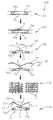
제 5도는 본 발명에 따른 측면 발광형 엘이디 패키지를 도시한 측면도로서,5 is a side view showing a side-emitting type LED package according to the present invention,
a)도는 하나의 엘이디 칩을 광원으로 구비한 구조, a) a structure having a single LED chip as a light source,
b)도는 다수의 엘이디 칩을 광원으로 구비한 구조. b) is a structure having a plurality of LED chips as a light source.
제 6도는 본 발명에 따라서 하나의 엘이디 칩을 광원으로 구비한 측면 발광형 엘이디 패키지의 제조방법을 단계적으로 도시한 설명도.FIG. 6 is an explanatory diagram showing a step-by-step method of manufacturing a side-emitting type LED package having one LED chip as a light source according to the present invention.
제 7도는 본 발명에 따라서 다수 개의 엘이디 칩을 광원으로 구비한 측면 발광형 엘이디 패키지의 제조방법을 단계적으로 도시한 설명도.7 is an explanatory diagram illustrating a step-by-step method of manufacturing a side-emitting type LED package having a plurality of LED chips as a light source according to the present invention.
<도면의 주요부분에 대한 부호의 설명> <Description of Symbols for Main Parts of Drawings>
1.... 본 발명에 따른 측면 발광형 엘이디 패키지1 .... side emitting type LED package according to the present invention
5.... 광원 10.... 몰딩 부5 .... light source 10 .... molding part
15... 기판 15a... 전극15
17... 투광 면 20.... 반사 층17
100~112,150~162.. 본 발명의 제조 단계100-112,150-162. Production Steps of the Invention
200,230,260,300..... 종래의 측면 발광형 엘이디 패키지200,230,260,300 ..... Conventional side-emitting LED package
205... 광원 210.... 기판205
212... 렌즈 232.... 기판212
235... 몰딩 부 237.... 반사 필름235
240.... 광원 262,304.... 몰딩 부240 .... light source 262,304 .... molding part
265,308.... 반사 층 270,302.... 엘이디 칩265,308 .... Reflective layer 270,302 .... LED chip
272,314.... 리드 단자 310.... 투광 면272,314 ....
본 발명은 측 방향으로 광을 투사시키도록 된 측면 발광형 엘이디 패키지 및 그 제조 방법에 관한 것으로, 보다 상세히는 광을 측 방향으로 반사시키는 반사 층을 원하는 모양으로 쉽게 제작할 수 있고, 엘이디 칩 사이즈의 영향 없이 소형으로 대량 생산이 가능하며, 엘이디 어레이 타입으로도 쉽게 제작이 가능하여 작업 생산성을 크게 향상시킨 측면 발광형 엘이디 패키지 및 그 제조 방법에 관한 것이다.The present invention relates to a side-emitting type LED package and a method of manufacturing the same, which are configured to project light in a lateral direction, and more particularly, it is possible to easily produce a reflective layer reflecting light in a lateral direction, The present invention relates to a side-emitting LED package and a method of manufacturing the same, which can be mass-produced in a small size without any influence, and can be easily manufactured as an LED array type, thereby greatly improving work productivity.
현재 엘시디 백라이트 유닛(LCD BLU)용으로 엘이디 패키지 사용량이 점차적으로 증가되고 있다. 이러한 엘시디 백라이트 유닛용으로 쓰이는 고출력 패키지(High Power PKG)는 히트 슬러그(heat slug)를 장착한 패키지(PKG)에Currently, LED package usage for LCD backlight unit (LCD BLU) is gradually increasing. The high power package used for the LCD backlight unit is a package (PKG) equipped with a heat slug.
렌즈(lens)를 덮어 직하형 사이드 에미터(side emitter) 방식을 쓰고 있는 관계로 두께가 상당히 두꺼운 문제점이 있다. 그리고, 엘시디 백라이트 유닛의 두께가 점차적으로 슬림(slim)화 되려는 추세에 따라 엘시디 백라이트 유닛용으로 사용되는 엘이디 패키지(LED PKG)의 두께 또한 점차적으로 얇아지려고 하는 추세이다.There is a problem in that the thickness is considerably thick because the lens is covered with a direct side emitter method. In addition, as the thickness of the LCD backlight unit is gradually slimmed, the thickness of the LED package (LED PKG) used for the LCD backlight unit is gradually decreasing.
도 1a)에는 종래의 기술에 따른 측면 발광형 엘이디 패키지(200)가 도시되어 있다. 이러한 종래의 구조는 엘이디 칩(205)이 장착되는 기판(210) 위에 렌즈(212)를 덮는 구조로서 기판(210)에 렌즈(212)를 부착하는 공정이 추가되어 별도의 렌즈 (212)를 제작하는 문제 및 렌즈(212)를 붙이는 조립 작업이 번거롭다. Figure 1a) is a side-emitting
도 1b)에는 이와는 다른 종래의 엘이디 패키지(230) 구조가 도시되어 있다. 이러한 종래 기술은 기판(232) 위의 몰딩 부(235)에 평판형 반사 필름(237)을 형성하는 구조로서, 이러한 방식도 엘이디 칩(240)으로부터의 광이 상기 반사 필름에 반사되어 측 방향으로 효율적으로 반사시키는 데에는 문제점이 있다. 1b) illustrates another
도 2a)에는 상기와는 다른 또 다른 구조의 엘이디 패키지(260)가 도시되어 있다. 이러한 종래의 구조는 일본 특개평 10-82916호에 기재되어 있는 내용으로서, 몰딩 부(262)의 상부 면에 오목한 홈을 형성하고, 상기 홈에는 광 반사 층(265)이 형성되어 측면 사방에 걸쳐서 투광 면을 형성하는 구조이다. 그렇지만, 이와 같은 종래의 구조는 광 반사 층(265)이 몰딩 부(262)의 중앙 일부에만 걸쳐 있는 구조이고, 이는 엘이디 칩(270)이 사다리꼴 리드 단자(272)에 장착된 것이다. 2A), another structure of the
그러나 이와 같은 종래의 구조는 광을 상부 방향이 아닌 측 방향으로 투사시키는 데에 한계가 있는 것이고, 리드 단자로 구성되어 시간당 생산량이 떨어지는 문제점이 있는 것이다. However, such a conventional structure has a limitation in projecting light in the lateral direction rather than in the upper direction, and has a problem in that the yield per hour is reduced because it is composed of lead terminals.
또한 도 2b)에는 또 다른 종래의 엘이디 패키지(300)가 도시되어 있다. 이는 Methew L. Sommers 에게 부여된 미국 특허 제6674096호에 관한 것으로서, 엘이디 칩(302)을 투명한 몰딩 부(304)가 감싸고, 상기 몰딩 부(304)의 상부 면에는 중앙이 오목한 반사 면(306)이 형성되며, 상기 반사 면(306)에는 반사 층(308)이 형성되어 측면 사방에 걸쳐서 투광 면(310)을 형성하도록 된 것이다. Also shown in FIG. 2B is another
그렇지만, 이와 같은 종래의 기술도 광이 상부 측으로 분산됨으로써 광을 측 방향으로 효과적으로 유도시키는 데에는 한계가 있는 것이고, 리드 단자로 구성되어 시간당 생산량이 떨어지는 문제점이 있다. However, this conventional technique also has a limit in effectively inducing the light in the lateral direction by dispersing the light to the upper side, and has a problem in that the yield per hour is reduced because it is composed of lead terminals.
본 발명은 상기와 같은 종래의 문제점을 해소하기 위한 것으로서, 그 목적은 광이 반사 층의 상부로 분산되는 것을 방지하고, 효과적으로 측 방향으로 반사시킬 수 있는 측면 발광형 엘이디 패키지 및 그 제조 방법을 제공함에 있다. The present invention is to solve the conventional problems as described above, the object of the present invention is to provide a side-emitting type LED package and a method of manufacturing the same that can prevent the light is dispersed to the top of the reflective layer, and can effectively reflect laterally Is in.
그리고 본 발명은 몰딩 부를 원하는 모양으로 쉽게 제작할 수 있고, PCB 타입으로 대량 생산이 가능한 측면 발광형 엘이디 패키지 및 그 제조 방법을 제공함에 있다. In another aspect, the present invention is to provide a side-emitting LED package and a method of manufacturing the molding unit can be easily produced in a desired shape, mass production in a PCB type.
또한 본 발명은 EMC(Epoxy Molding Compound) 트랜스퍼 몰딩법을 채택함으로써 색산포의 최소화가 가능한 측면 발광형 엘이디 패키지 및 그 제조 방법을 제공함에 있다. In another aspect, the present invention provides a side-emitting LED package and a method of manufacturing the same that can be minimized by adopting the EMC (Epoxy Molding Compound) transfer molding method.
상기와 같은 목적을 달성하기 위하여 본 발명은, 광원으로부터 나온 광을 측 방향으로 투사시키기 위한 엘이디 패키지에 있어서,In order to achieve the above object, the present invention, in the LED package for projecting the light from the light source in the lateral direction,
전극이 형성된 기판;A substrate on which an electrode is formed;
상기 기판상에 전기적으로 연결 배치된 광원;A light source electrically connected to and disposed on the substrate;
상기 기판과 광원을 덮어 보호하고 중앙이 오목한 상부 면을 형성한 몰딩 부; 및A molding part covering and protecting the substrate and the light source and forming a concave upper surface; And
상기 몰딩 부의 상부 면 전체를 덮고, 상기 몰딩 부의 측면으로 광을 반사하는 투광 면을 형성한 반사 층;을 포함하는 것을 특징으로 하는 측면 발광형 엘이디 패키지를 제공한다. And a reflective layer covering the entire upper surface of the molding part and forming a transmissive surface for reflecting light toward the side of the molding part.
그리고 본 발명은 상기 목적을 달성하기 위하여, 광원으로부터 나온 광을 측 방향으로 투사시키기 위한 엘이디 패키지의 제조방법에 있어서, And in order to achieve the above object, in the manufacturing method of the LED package for projecting the light from the light source in the lateral direction,
전극이 형성된 기판을 제공하는 단계 ; Providing a substrate on which an electrode is formed;
상기 기판상에 둘 이상의 광원을 배치하는 단계; Placing at least two light sources on the substrate;
상기 광원과 기판 위에, 상기 광원과 대응되는 상부면 중앙이 오목한 형상을 갖는 몰딩부를 형성하는 단계; Forming a molding part on the light source and the substrate, the molding part having a concave shape at the center of the upper surface corresponding to the light source;
상기 몰딩 부의 상부 면을 전체적으로 덮는 반사 층을 형성하는 단계; 그리고 Forming a reflective layer covering the upper surface of the molding portion as a whole; And
상기 둘 이상의 광원이 각각 개별적인 패키지로 구획되도록, 상기 기판, 몰딩 부 및 반사 층을 동시에 절단하여 측면에 투광 면을 형성하는 단계;를 포함하는 것을 특징으로 하는 측면 발광형 엘이디 패키지의 제조방법을 제공한다. Providing a light emitting surface on the side by simultaneously cutting the substrate, the molding part and the reflective layer such that the two or more light sources are partitioned into separate packages, respectively. do.
이하, 본 발명의 바람직한 실시 예들을 도면을 참조하여 보다 상세히 설명하기로 한다.Hereinafter, preferred embodiments of the present invention will be described in detail with reference to the drawings.
본 발명에 따른 측면 발광형 엘이디 패키지(1)는 도 3 내지 도 5에 도시된 바와 같이, 광원(5)을 이루는 엘이디 칩으로부터 나온 광을 몰딩 부(10)의 측 방향으로 투사시키기 위한 것이다. 광의 투사 방향은 바람직하게는 상기 엘이디 칩이 배치되는 평면에 대해 나란한 측 방향이다.As shown in FIGS. 3 to 5, the side-emitting
본 발명에 따른 측면 발광형 엘이디 패키지(1)는 전극(15a)이 형성된 기판(15)을 갖는다. 상기 기판(15)은 바람직하게는 패턴 전극, 또는 비아 홀 형태의 수직전극(15a)이 형성된 PCB 이거나 세라믹 재료로 이루어질 수 있다.The side-emitting
그리고 상기 기판(15)상에는 전극(15a)에 전기적으로 연결 배치된 엘이디 칩이 광원(5)으로서 실장되며, 상기 엘이디 칩은 그 전기 단자들이 모두 상부 면에 형성된 수평형 타입(Horizontal type)이거나, 또는 상,하부 면에 형성된 수직형 타입(Vertical type) 모두 적용 가능하다.An LED chip electrically connected to the
또한 이러한 상기 광원(5)과 기판(15)상에는 이들을 덮어 보호하는 몰딩 부(10)가 형성된다. 상기 몰딩 부(10)는 수지 등을 경화시켜 이루어지는 것으로서, 바람직하게는 형광체가 혼합된 투명 EMC(Epoxy Molding Compound) 층으로 이루어지고, 이와 같이 몰딩 부(10)를 형성하여 색 산포의 최소화를 이룬다.In addition, a
본 발명은 이러한 몰딩 부(10)를 형성하는 과정에서 상기 몰딩 부(10)를 이루는 몰드(미 도시)의 형태를 다양하게 할 수 있다. 예를 들면, 도 3의 a),b)에 도시된 바와 같이, 상부 면의 중앙이 오목한 원추형 곡면을 갖는 형태로 하거나, 도 3의 c)에 도시된 바와 같이, 상부 면의 중앙과 상부 면 테두리 중앙이 오목하고, 상부 면 모서리 부분은 볼록한 형태로 형성될 수 있으며, 이는 이후에 제조방법에서 설명되는 바와 같이, 상기 몰딩 부(10)를 형성시키는 몰드(미 도시)의 형태를 이러한 몰딩 부(10) 구조에 맞추어 사전에 가공하여 사용함으로써 원하는 형태로 형성할 수 있다.The present invention may vary the shape of a mold (not shown) forming the
또한 상기와 같이 몰딩 부(10)가 어느 한 가지 형태로 형성되면, 그 위에 상기 몰딩 부(10)의 외면을 덮도록 반사 층(20)을 형성하게 된다. 상기 반사 층(20)은 Al,Au,Ag,Ni,W,Ti,Pt 등의 금속 증착 등을 통하여 형성되거나, 또는 박막 등을 상기 몰딩 부(10)의 상부 면에 직접 부착 또는 에워싸도록 형성(encapsulation) 하여 이루어진다. 상기 반사 층(20)은 몰딩 부(10)의 상부 면을 완전하게 감싸서 광의 상부로의 누출을 차단하고, 광원의 측 방향으로 투광 면(17)을 형성한 구조이다.In addition, when the
상기에서 투광 면(17)은 광원(5)을 이루는 엘이디 칩 또는 광원(5)이 장착된 기판(15)의 평면에 대해 나란한 측 방향으로 바람직하게 형성된다. 또한 상기 투광 면(17)은 도 3및 도 4에 도시된 바와 같이, 둥근 원주면을 형성하거나, 다각형의 각형 면을 형성할 수 있다.The
바람직하게는 상기 반사 층(20), 몰딩 부(10) 및 기판(15)이 형성하는 외주 형상은 서로 동일하여 상기 반사 층(20)이 몰딩 부(10)의 상부 면을 완전히 막아 주므로 상부로의 광의 누설을 방지하는 것이다.Preferably, the outer circumferential shapes formed by the
그리고 본 발명의 측면 발광형 엘이디 패키지(1)는 상기 몰딩 부(10) 내에, 도 5a)에 도시된 바와 같이 광원(5)을 이루기 위하여 하나의 엘이디 칩을 구비하거나, 또는 광학 설계적인 요구 조건에 맞추어 도 5b)에 도시된 바와 같이 다수 개의 엘이디 칩을 구비할 수 있다.And the side-emitting
이하, 본 발명에 따른 측면 발광형 엘이디 패키지의 제조방법에 관하여 상세히 설명한다. Hereinafter, a method of manufacturing a side emitting type LED package according to the present invention will be described in detail.
본 발명에 따른 측면 발광형 엘이디 패키지의 제조방법(100)은 도 6에 도시된 바와 같이, 먼저 하나의 몰딩 부(10)와 반사 층(20)의 내부에 광원(5)을 이루기 위해 하나의 엘이디 칩을 구비하여 제작가능하다. As shown in FIG. 6, the
본 발명에 따른 측면 발광형 엘이디 패키지의 제조방법(100)은 전극(15a)이 형성된 기판(15)을 제공하는 단계(102)가 이루어진다. 상기 기판(15)은 비아 홀 등의 수직 전극과 패턴 전극(15a)이 형성된 PCB이거나 패턴 전극(15a)이 형성된 세라믹 재료 등으로 이루어질 수 있으며, 광원(5)을 이루는 엘이디 칩들이 실장되는 지점에는 각각 비아 홀(Via Holes) 등의 수직 전극을 형성하고 있다. In the
그리고 상기 기판(15)상에는 둘 이상의 즉, 다수의 광원(5)을 배치하는 단계(104)가 이루어진다. A
이는 하나의 기판(15)상에 다수의 광원(5)을 이루기 위하여 다수의 엘이디 칩들이 일시에 실장 되고, 상기 기판(15)의 전극(15a)에 각각 광원(5)들이 전기적으로 연결 배선된다. This is because a plurality of LED chips are mounted at one time to form a plurality of
그 다음으로는 상기와 같은 광원(5)과 기판(15) 위에 몰딩 부(10)를 형성하는 단계(106)가 이루어진다. 이 단계(106)에서 상기 몰딩 부(10)는 바람직하게는 형광체(Phosphor)가 혼합된 투명 EMC(Epoxy Molding Compound) 트랜스퍼 몰딩법으로서 형성되어 경화된 후의 색 산포를 최소화하는 것이다. Next, a
또한 이와 같은 몰딩 부(10)에서 사용되는 몰드(미도시)는 도 3에 관련하여 설명한 바와 같이, 상부 면의 중앙이 오목한 원추형 곡면을 갖는 형태로 하거나, 상부 면의 중앙과 상부 면 테두리 중앙이 오목하고, 상부 면 모서리 부분은 볼록한 형태로 다양하게 구성할 수 있는 것이다. In addition, the mold (not shown) used in the
그리고, 다음으로는 상기 몰딩 부(10)의 외면에, 예를 들면 Al,Au,Ag,Ni,W, Next, on the outer surface of the
Ti,Pt 등의 반사율이 높은 금속을 금속 증착으로 형성하거나, 또는 반사율이 높은 별도의 박막 등을 상기 몰딩 부(10)에 부착 또는 에워싸도록 형성시키는 단계(108)가 이루어진다. 또한 이와 같이 몰딩 부(10)를 형성한 다음에는 상기 둘 이상의 광원(5)이 각각 개별적인 패키지로 구획되도록 상기 기판(15), 몰딩 부(10) 및 반사 층(20)을 동시에 절단하는 단계(110)가 이루어진다.A
상기 절단 단계(110)는 생산하고자 하는 본 발명의 측면 발광형 엘이디 패키지 형태에 따라서, 다이싱(dicing), 브레이킹(breaking), 또는 레이저 절단(Laser Cutting) 등이 이루어진다. In the cutting step 110, dicing, breaking, or laser cutting may be performed according to the shape of the side-emitting type LED package of the present invention.
즉, 본 발명에 따른 측면 발광형 엘이디 패키지(1)의 형태가 사각 각형을 이루는 경우는, 단계(110)에서와 같이 기판(15), 몰딩 부(10) 및 반사 층(20)을 동시에 좌,우방향으로 다이싱 또는 브레이킹하여 하나의 본 발명의 측면 발광형 엘이디 패키지(1)를 분리 제작한다. 이와 같이 상기 기판(15), 몰딩 부(10) 및 반사 층(20)이 동시에 절단되면, 절단된 몰딩 부(10)의 측면은 반사 층(20)에 의해 덮이지 아니하고 외부로 노출된 상태가 되므로, 상기 광원(5)의 빛이 투광되는 투광면이 된다. That is, in the case where the shape of the side-emitting
또는, 상기와는 다르게 본 발명에 따른 측면 발광형 엘이디 패키지(1)가 둥근 원주의 투광 면(17)을 갖는 것이라면, 레이저 가공으로 기판(15), 몰딩 부(10) 및 반사 층(20)들을 동시에 절단처리한다. Alternatively, if the side-emitting
이와 같이, 상기 기판(15), 몰딩 부(10) 및 반사 층(20)들을 절단 처리하면, 광원(5)으로서 하나의 엘이디 칩을 내장한 측면 발광형 엘이디 패키지(1)가 단계(112)에서와 같이 제작되는 것이다. As such, when the
이와 같이 제작된 본 발명의 측면 발광형 엘이디 패키지(1)는 반사 층(20)이 몰딩 부(10)의 상부 면을 완전히 덮고 있으므로, 광원(5)인 엘이디 칩으로 부터 발광된 광이 반사 층(20)의 상부로 분산되는 것을 방지하고, 효과적으로 측 방향으로 반사시킬 수 있다. Since the
그리고 기판(15), 몰딩 부(10) 및 반사 층(20)들을 PCB 타입으로 대량 생산이 가능하여 작업 생산성을 높게 할 수 있다. 뿐만 아니라, 몰딩 부(10)에서 색산포의 최소화가 가능하여 발광 성능이 우수한 측면 발광형 엘이디 패키지(1)를 제공할 수 있다. In addition, since the
또한 도 7에는 본 발명에 따른 측면 발광형 엘이디 패키지의 제조방법(150)이 단계적으로 도시되어 있으며, 이는 하나의 몰딩 부(10)와 반사 층(20)의 내부에 광원(5)을 이루기 위해 다수 개의 엘이디 칩들이 내장된 것이다. In addition, FIG. 7 illustrates a
이러한 측면 발광형 엘이디 패키지의 제조방법(150)은 도 6에 관련하여 설명한 바와 같이, 먼저 전극(15a)이 형성된 기판(15)을 제공하는 단계(152)가 이루어진다. In the
그리고 상기 기판(15)에는 광원(5)을 이루는 엘이디 칩들이 장착되는 지점 에, 전극(15a)이 구비되고, 다수의 비아 홀(Via Holes)들이 각각 형성되어 수직 전극을 형성한다. An
또한 다음으로는 상기 기판(15)상에 광원(5)을 이루는 다수 개의 엘이디 칩들을 배치하고, 상기 각각의 엘이디 칩들을 기판(15)의 전극(15a)에 와이어들을 이용하여 전기적으로 배선하는 단계(154)가 이루어진다. Next, a plurality of LED chips forming a
그 다음으로는 상기와 같은 광원(5)과 기판(15) 위에 몰딩 부(10)를 형성하는 단계(156)가 이루어지게 되며, 상기 몰딩 부(10)는 투명 EMC(Epoxy Molding Compound) 트랜스퍼 몰딩법으로서 형성되는 것이다. Next, a step 156 of forming the
또한 다음으로는 도 6에 관련하여 설명한 바와 같이, 상기 몰딩 부(10)의 외면에, 예를 들면 Al,Au,Ag,Ni,W,Ti,Pt 등의 반사율이 높은 금속을 증착으로 형성하거나, 또는 반사율이 높은 별도의 박막 등을 상기 몰딩 부(10)에 부착 또는 에워싸도록 형성시키는 단계(158)가 이루어진다. Next, as described with reference to FIG. 6, a metal having a high reflectance such as Al, Au, Ag, Ni, W, Ti, or Pt may be formed on the outer surface of the
그리고 마지막으로 상기 기판(15), 몰딩 부(10)와 반사 층(20)들을 절단하여 측면에 투광 면(17)을 형성하는 단계(160)가 이루어지는 것이다. Finally, a
상기와 같이 기판(15), 몰딩 부(10)와 반사 층(20)들을 절단하면 다수 개의 엘이디 칩들로 이루어진 광원(5)을 내장한 측면 발광형 엘이디 패키지(1) 들이 단계(162)에서와 같이 다수 개 제작되는 것이다. When the
이와 같이 제작된 본 발명의 측면 발광형 엘이디 패키지(1)는 반사 층(20)이 몰딩 부(10)의 상부 면을 완전히 덮고 있으므로, 광원(5)으로 부터 발광된 광이 반사 층(20)의 상부로 분산되는 것을 방지하고, 효과적으로 측 방향의 투광 면(17)으 로 반사시킬 수 있다. Since the
그리고, 상기 기판(15), 몰딩 부(10)와 반사 층(20)들을 PCB 타입으로 대량 생산이 가능하여 작업 생산성을 높게 할 수 있고, 몰딩 부(10)에서 색 산포의 최소화가 가능하며, 광원(5)으로서 다수 개의 엘이디 칩들을 사용할 수 있어서 발광 성능이 우수한 측면 발광형 엘이디 패키지(1)를 제공할 수 있다. In addition, the
또한, 광원(5)을 이루는 엘이디 칩들을 레드(Red), 그린(Green), 블루(Blue)로 실장하여 백색광(White)의 구현이 가능한 효과를 얻는다. In addition, the LED chips constituting the
뿐만 아니라, 제어 다이오드(Zener Diode)도 함께 실장가능한 것이다. In addition, the control diode (Zener Diode) can be mounted together.
상기와 같이 본 발명에 의하면, 몰딩 부에 부착되는 사출 물 등이 불필요하여 사출 물에 의한 제약을 받지 않으므로 소형화된 박형(Thin) 구조가 가능하고, 투광 면이 광원을 이루는 엘이디 칩의 장착 평면의 측 방향으로 형성되기 때문에 엘이디 칩 사이즈의 영향 없이 얇은 두께로 제작 가능하다. As described above, according to the present invention, since the injection molding attached to the molding part is unnecessary and is not restricted by the injection molding, a miniaturized thin structure is possible, and the light emitting surface of the LED chip having the light emitting surface is a light source. Since it is formed laterally, it can be manufactured in a thin thickness without the influence of the LED chip size.
그리고, 기판을 PCB 공정상태로, 즉 엘이디 칩의 실장 공정부터 그 이후의 몰딩 및 절단 공정까지 PCB 상태로 이루어지므로 대량 생산이 가능하며, 어레이 타입(Array Type)의 엘이디 패키지로 제작이 용이한 것이다. In addition, since the substrate is in the PCB process state, that is, the PCB state from the mounting process of the LED chip to the molding and cutting process thereafter, the mass production is possible, and it is easy to manufacture the LED package of the array type. .
그리고 본 발명은 몰딩 부를 형성하는 몰드(미 도시)의 형태를 자유롭게 제 작하여 몰딩 부의 형태를 다양하게 하고, 그에 따라 몰딩 부에 형성되는 반사 층의 형상을 원하는 모양으로 쉽게 제작할 수 있다. In addition, the present invention may freely form a mold (not shown) forming the molding part, thereby varying the shape of the molding part, thereby easily forming a shape of the reflective layer formed on the molding part in a desired shape.
뿐만 아니라, 본 발명은 형광체와 혼합되는 투명 EMC(Epoxy Molding Compound) 트랜스퍼 몰딩법을 채택함으로써 경화 후의 몰딩 부에서 색 산포의 최소화가 가능하여 광학 품질도 크게 향상되는 효과가 얻어지는 것이다. In addition, the present invention adopts a transparent EMC (Epoxy Molding Compound) transfer molding method to be mixed with a phosphor, thereby minimizing color scattering in the molding part after curing, thereby greatly improving the optical quality.
상기에서 본 발명은 특정한 실시 예에 관하여 도시되고 설명되었지만, 이는 단지 예시적으로 본 발명을 설명하기 위하여 기재된 것이며, 본 발명을 이와 같은 특정 구조로 제한하려는 것은 아니다. 당 업계에서 통상의 지식을 가진 자라면 이하의 특허청구범위에 기재된 본 발명의 사상 및 영역을 벗어나지 않는 범위 내에서 본 발명을 다양하게 수정 및 변경시킬 수 있음을 알 수 있을 것이다. 그렇지만 이러한 수정 및 변형 구조들은 모두 본 발명의 권리범위 내에 포함되는 것 임을 분명하게 밝혀두고자 한다. While the invention has been shown and described with respect to specific embodiments thereof, it has been described by way of example only to illustrate the invention, and is not intended to limit the invention to this particular structure. Those skilled in the art will appreciate that various modifications and changes of the present invention can be made without departing from the spirit and scope of the invention as set forth in the claims below. Nevertheless, it will be clearly understood that all such modifications and variations are included within the scope of the present invention.
Claims (12)
Translated fromKoreanPriority Applications (4)
| Application Number | Priority Date | Filing Date | Title |
|---|---|---|---|
| KR1020050046618AKR100691179B1 (en) | 2005-06-01 | 2005-06-01 | Side emitting type LED package and manufacturing method thereof |
| JP2006152714AJP4676386B2 (en) | 2005-06-01 | 2006-05-31 | Side-emitting LED package and manufacturing method thereof |
| US11/444,402US20060273337A1 (en) | 2005-06-01 | 2006-06-01 | Side-emitting LED package and method of manufacturing the same |
| US12/155,961US7833811B2 (en) | 2005-06-01 | 2008-06-12 | Side-emitting LED package and method of manufacturing the same |
Applications Claiming Priority (1)
| Application Number | Priority Date | Filing Date | Title |
|---|---|---|---|
| KR1020050046618AKR100691179B1 (en) | 2005-06-01 | 2005-06-01 | Side emitting type LED package and manufacturing method thereof |
Publications (2)
| Publication Number | Publication Date |
|---|---|
| KR20060124925A KR20060124925A (en) | 2006-12-06 |
| KR100691179B1true KR100691179B1 (en) | 2007-03-09 |
Family
ID=37493287
Family Applications (1)
| Application Number | Title | Priority Date | Filing Date |
|---|---|---|---|
| KR1020050046618AExpired - LifetimeKR100691179B1 (en) | 2005-06-01 | 2005-06-01 | Side emitting type LED package and manufacturing method thereof |
Country Status (3)
| Country | Link |
|---|---|
| US (2) | US20060273337A1 (en) |
| JP (1) | JP4676386B2 (en) |
| KR (1) | KR100691179B1 (en) |
Cited By (1)
| Publication number | Priority date | Publication date | Assignee | Title |
|---|---|---|---|---|
| WO2010117167A3 (en)* | 2009-04-10 | 2011-02-17 | Kim Duk-Yong | Led lighting apparatus, and surface emitting method for the led lighting apparatus |
Families Citing this family (66)
| Publication number | Priority date | Publication date | Assignee | Title |
|---|---|---|---|---|
| TWI313775B (en)* | 2005-01-06 | 2009-08-21 | Au Optronics Corp | Backlight module and illumination device thereof |
| US8215815B2 (en) | 2005-06-07 | 2012-07-10 | Oree, Inc. | Illumination apparatus and methods of forming the same |
| WO2006131924A2 (en) | 2005-06-07 | 2006-12-14 | Oree, Advanced Illumination Solutions Inc. | Illumination apparatus |
| US8272758B2 (en) | 2005-06-07 | 2012-09-25 | Oree, Inc. | Illumination apparatus and methods of forming the same |
| JP5108297B2 (en)* | 2005-12-27 | 2012-12-26 | 昭和電工株式会社 | Light emitting element mounting package, surface light source device, and display device |
| US7775687B2 (en)* | 2006-02-20 | 2010-08-17 | Nichia Corporation | Light emitting device |
| CN101669219B (en)* | 2006-12-22 | 2011-10-05 | 昆南诺股份有限公司 | LED with vertical nanowire structure and method of making the same |
| KR101309762B1 (en)* | 2007-03-29 | 2013-09-23 | 서울반도체 주식회사 | Led package with downwardly relfective surface |
| KR101322454B1 (en)* | 2007-03-30 | 2013-10-25 | 서울반도체 주식회사 | Light emitting diode package |
| RU2010119520A (en)* | 2007-10-16 | 2011-11-27 | Конинклейке Филипс Электроникс Н.В. (Nl) | LED LIGHT WITH LATERAL RADIATION FOR BACKLIGHT |
| EP2212928B1 (en)* | 2007-11-20 | 2016-06-29 | Koninklijke Philips N.V. | Side emitting device with wavelength conversion |
| WO2009074919A1 (en) | 2007-12-11 | 2009-06-18 | Koninklijke Philips Electronics N.V. | Side emitting device with hybrid top reflector |
| US8471281B2 (en) | 2007-12-11 | 2013-06-25 | Koninklijke Philips Electronics N.V. | Side emitting device with hybrid top reflector |
| US7907804B2 (en) | 2007-12-19 | 2011-03-15 | Oree, Inc. | Elimination of stitch artifacts in a planar illumination area |
| US8182128B2 (en)* | 2007-12-19 | 2012-05-22 | Oree, Inc. | Planar white illumination apparatus |
| TW200943591A (en)* | 2008-01-22 | 2009-10-16 | Alps Electric Co Ltd | Led package using light reflector |
| TW200945633A (en)* | 2008-02-27 | 2009-11-01 | Alps Electric Co Ltd | Light emitter and semiconductor light-emitting device using same |
| DE102008011862A1 (en)* | 2008-02-29 | 2009-09-03 | Osram Opto Semiconductors Gmbh | Miniature housing, carrier assembly with at least one miniature housing, and a method for producing a carrier assembly |
| US20090225566A1 (en) | 2008-03-05 | 2009-09-10 | Micha Zimmermann | Illumination apparatus and methods of forming the same |
| TWI363852B (en)* | 2008-03-28 | 2012-05-11 | Ind Tech Res Inst | Stacked light emitting device |
| JP5187749B2 (en)* | 2008-07-02 | 2013-04-24 | Necライティング株式会社 | Light emitting device |
| US8301002B2 (en) | 2008-07-10 | 2012-10-30 | Oree, Inc. | Slim waveguide coupling apparatus and method |
| US8297786B2 (en)* | 2008-07-10 | 2012-10-30 | Oree, Inc. | Slim waveguide coupling apparatus and method |
| KR100902908B1 (en)* | 2008-07-17 | 2009-06-15 | 엘지전자 주식회사 | Light emitting device package and backlight unit using same |
| JP2010045248A (en)* | 2008-08-14 | 2010-02-25 | Citizen Electronics Co Ltd | Light-emitting diode |
| US7837370B2 (en)* | 2008-10-10 | 2010-11-23 | Koninklijke Philips Electronics N.V. | Low profile side emission TIR lens for LED |
| US20100320904A1 (en) | 2009-05-13 | 2010-12-23 | Oree Inc. | LED-Based Replacement Lamps for Incandescent Fixtures |
| US8922106B2 (en)* | 2009-06-02 | 2014-12-30 | Bridgelux, Inc. | Light source with optics to produce a spherical emission pattern |
| JP5382787B2 (en) | 2009-06-05 | 2014-01-08 | シチズン電子株式会社 | Planar light source and liquid crystal display device |
| WO2010150202A2 (en) | 2009-06-24 | 2010-12-29 | Oree, Advanced Illumination Solutions Inc. | Illumination apparatus with high conversion efficiency and methods of forming the same |
| EP2270882A1 (en)* | 2009-06-30 | 2011-01-05 | Koninklijke Philips Electronics N.V. | Light emitting diode circuit for ambient light |
| KR101028304B1 (en)* | 2009-10-15 | 2011-04-11 | 엘지이노텍 주식회사 | Light emitting apparatus |
| KR101615497B1 (en)* | 2009-11-27 | 2016-04-27 | 삼성전자주식회사 | Light Emitting Diode Package and Method of Manufacturing The Same |
| TWI561770B (en)* | 2010-04-30 | 2016-12-11 | Samsung Electronics Co Ltd | Light emitting device package, light source module, backlight unit, display apparatus, television set, and illumination apparatus |
| DE102010032041A1 (en) | 2010-07-23 | 2012-01-26 | Osram Opto Semiconductors Gmbh | Radiation-emitting component and method for the production of radiation-emitting Bauelemnenten |
| US10147853B2 (en) | 2011-03-18 | 2018-12-04 | Cree, Inc. | Encapsulant with index matched thixotropic agent |
| US9004724B2 (en)* | 2011-03-21 | 2015-04-14 | GE Lighting Solutions, LLC | Reflector (optics) used in LED deco lamp |
| US8497519B2 (en)* | 2011-05-24 | 2013-07-30 | Tsmc Solid State Lighting Ltd. | Batwing LED with remote phosphor configuration |
| US8591072B2 (en) | 2011-11-16 | 2013-11-26 | Oree, Inc. | Illumination apparatus confining light by total internal reflection and methods of forming the same |
| JP2013110179A (en)* | 2011-11-18 | 2013-06-06 | Citizen Holdings Co Ltd | Semiconductor light-emitting device |
| JP2013115088A (en)* | 2011-11-25 | 2013-06-10 | Citizen Holdings Co Ltd | Semiconductor light-emitting device |
| US8796052B2 (en) | 2012-02-24 | 2014-08-05 | Intersil Americas LLC | Optoelectronic apparatuses with post-molded reflector cups and methods for manufacturing the same |
| CN103311399B (en)* | 2012-03-15 | 2015-10-07 | 展晶科技(深圳)有限公司 | LED lighting device |
| US10468565B2 (en) | 2012-06-11 | 2019-11-05 | Cree, Inc. | LED package with multiple element light source and encapsulant having curved and/or planar surfaces |
| US9818919B2 (en) | 2012-06-11 | 2017-11-14 | Cree, Inc. | LED package with multiple element light source and encapsulant having planar surfaces |
| US9887327B2 (en) | 2012-06-11 | 2018-02-06 | Cree, Inc. | LED package with encapsulant having curved and planar surfaces |
| US10424702B2 (en) | 2012-06-11 | 2019-09-24 | Cree, Inc. | Compact LED package with reflectivity layer |
| JP2012227537A (en)* | 2012-06-19 | 2012-11-15 | Mitsubishi Electric Corp | Led light source and luminous body using the same |
| WO2014006501A1 (en) | 2012-07-03 | 2014-01-09 | Yosi Shani | Planar remote phosphor illumination apparatus |
| US8889439B2 (en)* | 2012-08-24 | 2014-11-18 | Tsmc Solid State Lighting Ltd. | Method and apparatus for packaging phosphor-coated LEDs |
| CN102937269A (en)* | 2012-11-15 | 2013-02-20 | 京东方科技集团股份有限公司 | Light guide plate, backlight module and display device |
| TW201500776A (en)* | 2013-06-28 | 2015-01-01 | 鴻海精密工業股份有限公司 | Lens and light source module with the same |
| EP3028302B1 (en)* | 2013-08-01 | 2022-01-05 | CreeLED, Inc. | Light emitting diode package with encapsulant having curved and planar surfaces |
| US9461024B2 (en) | 2013-08-01 | 2016-10-04 | Cree, Inc. | Light emitter devices and methods for light emitting diode (LED) chips |
| JP6273124B2 (en) | 2013-11-08 | 2018-01-31 | シチズン電子株式会社 | LED lighting device |
| TWI707484B (en) | 2013-11-14 | 2020-10-11 | 晶元光電股份有限公司 | Light-emitting device |
| KR102277127B1 (en)* | 2014-10-17 | 2021-07-15 | 삼성전자주식회사 | Light emitting device package |
| JP6665690B2 (en)* | 2016-05-31 | 2020-03-13 | 日亜化学工業株式会社 | Lighting equipment |
| JP2018207005A (en)* | 2017-06-07 | 2018-12-27 | シチズン電子株式会社 | Light-emitting device, manufacturing method thereof and planar light unit |
| CN109148674B (en) | 2017-06-28 | 2023-05-16 | 日亚化学工业株式会社 | light emitting device |
| JP7072368B2 (en)* | 2017-11-06 | 2022-05-20 | シチズン電子株式会社 | Side-illuminated LED light emitting device |
| JP7045198B2 (en)* | 2018-01-22 | 2022-03-31 | シチズン電子株式会社 | Side-illuminated LED light emitting device |
| TWI743540B (en)* | 2019-08-22 | 2021-10-21 | 友達光電股份有限公司 | Light-emitting unit and manufacturing method thereof |
| US11587362B2 (en) | 2020-12-16 | 2023-02-21 | Lenovo (Singapore) Pte. Ltd. | Techniques for determining sign language gesture partially shown in image(s) |
| US12159962B2 (en)* | 2021-12-16 | 2024-12-03 | DOMINANT Opto Technologies Sdn Bhd. | Side emitting LED package with bevel light emitting surface |
| US20240125457A1 (en)* | 2022-10-12 | 2024-04-18 | DOMINANT Opto Technologies Sdn Bhd. | Side emitting led package with shaped cap interface |
Citations (2)
| Publication number | Priority date | Publication date | Assignee | Title |
|---|---|---|---|---|
| JP2001185762A (en)* | 1999-12-24 | 2001-07-06 | Rohm Co Ltd | Back mount chip type light emitting device |
| JP2004140327A (en)* | 2002-08-21 | 2004-05-13 | Nippon Leiz Co Ltd | Light source, light guide, and planar light-emitting device |
Family Cites Families (16)
| Publication number | Priority date | Publication date | Assignee | Title |
|---|---|---|---|---|
| JPH1082916A (en) | 1996-09-06 | 1998-03-31 | Omron Corp | Surface light source device and liquid crystal display device |
| JP3868675B2 (en)* | 1999-08-19 | 2007-01-17 | ローム株式会社 | Manufacturing method of semiconductor light emitting device |
| DE10006738C2 (en)* | 2000-02-15 | 2002-01-17 | Osram Opto Semiconductors Gmbh | Light-emitting component with improved light decoupling and method for its production |
| JP2001257381A (en)* | 2000-03-13 | 2001-09-21 | Sharp Corp | Light emitting diode, method of manufacturing the same, and lighting device |
| CN1189951C (en)* | 2000-04-24 | 2005-02-16 | 罗姆股份有限公司 | Side emission type semiconductor light emitting device and manufacturing method thereof |
| TW459403B (en)* | 2000-07-28 | 2001-10-11 | Lee Jeong Hoon | White light-emitting diode |
| US6598998B2 (en)* | 2001-05-04 | 2003-07-29 | Lumileds Lighting, U.S., Llc | Side emitting light emitting device |
| US6989412B2 (en)* | 2001-06-06 | 2006-01-24 | Henkel Corporation | Epoxy molding compounds containing phosphor and process for preparing such compositions |
| US6674096B2 (en)* | 2001-06-08 | 2004-01-06 | Gelcore Llc | Light-emitting diode (LED) package and packaging method for shaping the external light intensity distribution |
| EP1453107A4 (en)* | 2001-11-16 | 2008-12-03 | Toyoda Gosei Kk | LIGHT EMITTING DIODE, DIODE LIGHTING AND LIGHTING DEVICE |
| JP2003158302A (en)* | 2001-11-21 | 2003-05-30 | Toyoda Gosei Co Ltd | Light emitting diode |
| JP4239563B2 (en)* | 2001-11-16 | 2009-03-18 | 豊田合成株式会社 | Light emitting diode and LED light |
| US20040223315A1 (en)* | 2003-03-03 | 2004-11-11 | Toyoda Gosei Co., Ltd. | Light emitting apparatus and method of making same |
| JP2004266124A (en)* | 2003-03-03 | 2004-09-24 | Matsushita Electric Ind Co Ltd | Semiconductor light emitting device |
| TWI324829B (en)* | 2004-02-06 | 2010-05-11 | Advanced Semiconductor Eng | Optical semiconductor package and method for manufacturing the same |
| KR20050082487A (en)* | 2004-02-19 | 2005-08-24 | 삼성전자주식회사 | Surface light source device and display device having the same |
- 2005
- 2005-06-01KRKR1020050046618Apatent/KR100691179B1/ennot_activeExpired - Lifetime
- 2006
- 2006-05-31JPJP2006152714Apatent/JP4676386B2/enactiveActive
- 2006-06-01USUS11/444,402patent/US20060273337A1/ennot_activeAbandoned
- 2008
- 2008-06-12USUS12/155,961patent/US7833811B2/enactiveActive
Patent Citations (2)
| Publication number | Priority date | Publication date | Assignee | Title |
|---|---|---|---|---|
| JP2001185762A (en)* | 1999-12-24 | 2001-07-06 | Rohm Co Ltd | Back mount chip type light emitting device |
| JP2004140327A (en)* | 2002-08-21 | 2004-05-13 | Nippon Leiz Co Ltd | Light source, light guide, and planar light-emitting device |
Non-Patent Citations (3)
| Title |
|---|
| 1020050046618 - 678164 |
| 13185762 |
| 일본특개평16-140327 * |
Cited By (1)
| Publication number | Priority date | Publication date | Assignee | Title |
|---|---|---|---|---|
| WO2010117167A3 (en)* | 2009-04-10 | 2011-02-17 | Kim Duk-Yong | Led lighting apparatus, and surface emitting method for the led lighting apparatus |
Also Published As
| Publication number | Publication date |
|---|---|
| US20080254558A1 (en) | 2008-10-16 |
| US20060273337A1 (en) | 2006-12-07 |
| JP2006339650A (en) | 2006-12-14 |
| JP4676386B2 (en) | 2011-04-27 |
| KR20060124925A (en) | 2006-12-06 |
| US7833811B2 (en) | 2010-11-16 |
Similar Documents
| Publication | Publication Date | Title |
|---|---|---|
| KR100691179B1 (en) | Side emitting type LED package and manufacturing method thereof | |
| KR100674871B1 (en) | Side emitting type LED package and manufacturing method thereof | |
| US11594665B2 (en) | Light-emitting unit and surface-emission light source | |
| US9039216B2 (en) | Light emitting device package and light unit having the same | |
| JP6186904B2 (en) | Light emitting device | |
| KR100818518B1 (en) | LED Package | |
| KR100638868B1 (en) | LED package having a metal reflective layer and a method of manufacturing the same | |
| JP4615981B2 (en) | Light emitting diode and manufacturing method thereof | |
| US20140306257A1 (en) | Led package and method for fabricating the same | |
| JP2012134531A (en) | Light emitting device | |
| EP3872873B1 (en) | Light-emitting module | |
| US11342314B2 (en) | Light-emitting module | |
| WO2012049853A1 (en) | Light-emitting device and surface light source device using same | |
| JP2017208568A (en) | Method for manufacturing light-emitting device | |
| JP5073242B2 (en) | Manufacturing method of light source device | |
| US11506933B2 (en) | Light-emitting module, method for manufacturing the same, and liquid-crystal display device | |
| KR20090073598A (en) | LED Package | |
| JP4938255B2 (en) | Light emitting element storage package, light source, and light emitting device | |
| JP2006352047A (en) | Optical semiconductor device | |
| KR20120136043A (en) | The light- |
Legal Events
| Date | Code | Title | Description |
|---|---|---|---|
| A201 | Request for examination | ||
| PA0109 | Patent application | Patent event code:PA01091R01D Comment text:Patent Application Patent event date:20050601 | |
| PA0201 | Request for examination | ||
| E902 | Notification of reason for refusal | ||
| PE0902 | Notice of grounds for rejection | Comment text:Notification of reason for refusal Patent event date:20060612 Patent event code:PE09021S01D | |
| PG1501 | Laying open of application | ||
| E701 | Decision to grant or registration of patent right | ||
| PE0701 | Decision of registration | Patent event code:PE07011S01D Comment text:Decision to Grant Registration Patent event date:20070126 | |
| GRNT | Written decision to grant | ||
| PR0701 | Registration of establishment | Comment text:Registration of Establishment Patent event date:20070228 Patent event code:PR07011E01D | |
| PR1002 | Payment of registration fee | Payment date:20070302 End annual number:3 Start annual number:1 | |
| PG1601 | Publication of registration | ||
| PR1001 | Payment of annual fee | Payment date:20091228 Start annual number:4 End annual number:4 | |
| PR1001 | Payment of annual fee | Payment date:20101215 Start annual number:5 End annual number:5 | |
| PR1001 | Payment of annual fee | Payment date:20120116 Start annual number:6 End annual number:6 | |
| FPAY | Annual fee payment | Payment date:20130131 Year of fee payment:7 | |
| PR1001 | Payment of annual fee | Payment date:20130131 Start annual number:7 End annual number:7 | |
| FPAY | Annual fee payment | Payment date:20140129 Year of fee payment:8 | |
| PR1001 | Payment of annual fee | Payment date:20140129 Start annual number:8 End annual number:8 | |
| FPAY | Annual fee payment | Payment date:20150202 Year of fee payment:9 | |
| PR1001 | Payment of annual fee | Payment date:20150202 Start annual number:9 End annual number:9 | |
| PR1001 | Payment of annual fee | Payment date:20220126 Start annual number:16 End annual number:16 | |
| PR1001 | Payment of annual fee | Payment date:20230125 Start annual number:17 End annual number:17 |