KR100689679B1 - Semiconductor device manufacturing method - Google Patents
Semiconductor device manufacturing methodDownload PDFInfo
- Publication number
- KR100689679B1 KR100689679B1KR1020050088344AKR20050088344AKR100689679B1KR 100689679 B1KR100689679 B1KR 100689679B1KR 1020050088344 AKR1020050088344 AKR 1020050088344AKR 20050088344 AKR20050088344 AKR 20050088344AKR 100689679 B1KR100689679 B1KR 100689679B1
- Authority
- KR
- South Korea
- Prior art keywords
- film
- gate
- silicon nitride
- nitride film
- semiconductor device
- Prior art date
- Legal status (The legal status is an assumption and is not a legal conclusion. Google has not performed a legal analysis and makes no representation as to the accuracy of the status listed.)
- Expired - Lifetime
Links
Images


Classifications
- H—ELECTRICITY
- H01—ELECTRIC ELEMENTS
- H01L—SEMICONDUCTOR DEVICES NOT COVERED BY CLASS H10
- H01L21/00—Processes or apparatus adapted for the manufacture or treatment of semiconductor or solid state devices or of parts thereof
- H01L21/02—Manufacture or treatment of semiconductor devices or of parts thereof
- H01L21/04—Manufacture or treatment of semiconductor devices or of parts thereof the devices having potential barriers, e.g. a PN junction, depletion layer or carrier concentration layer
- H01L21/18—Manufacture or treatment of semiconductor devices or of parts thereof the devices having potential barriers, e.g. a PN junction, depletion layer or carrier concentration layer the devices having semiconductor bodies comprising elements of Group IV of the Periodic Table or AIIIBV compounds with or without impurities, e.g. doping materials
- H01L21/28—Manufacture of electrodes on semiconductor bodies using processes or apparatus not provided for in groups H01L21/20 - H01L21/268
- H01L21/28008—Making conductor-insulator-semiconductor electrodes
- H01L21/28017—Making conductor-insulator-semiconductor electrodes the insulator being formed after the semiconductor body, the semiconductor being silicon
- H01L21/28247—Making conductor-insulator-semiconductor electrodes the insulator being formed after the semiconductor body, the semiconductor being silicon passivation or protection of the electrode, e.g. using re-oxidation
- H—ELECTRICITY
- H01—ELECTRIC ELEMENTS
- H01L—SEMICONDUCTOR DEVICES NOT COVERED BY CLASS H10
- H01L21/00—Processes or apparatus adapted for the manufacture or treatment of semiconductor or solid state devices or of parts thereof
- H01L21/02—Manufacture or treatment of semiconductor devices or of parts thereof
- H01L21/04—Manufacture or treatment of semiconductor devices or of parts thereof the devices having potential barriers, e.g. a PN junction, depletion layer or carrier concentration layer
- H01L21/18—Manufacture or treatment of semiconductor devices or of parts thereof the devices having potential barriers, e.g. a PN junction, depletion layer or carrier concentration layer the devices having semiconductor bodies comprising elements of Group IV of the Periodic Table or AIIIBV compounds with or without impurities, e.g. doping materials
- H01L21/30—Treatment of semiconductor bodies using processes or apparatus not provided for in groups H01L21/20 - H01L21/26
- H01L21/31—Treatment of semiconductor bodies using processes or apparatus not provided for in groups H01L21/20 - H01L21/26 to form insulating layers thereon, e.g. for masking or by using photolithographic techniques; After treatment of these layers; Selection of materials for these layers
Landscapes
- Engineering & Computer Science (AREA)
- Physics & Mathematics (AREA)
- Condensed Matter Physics & Semiconductors (AREA)
- General Physics & Mathematics (AREA)
- Manufacturing & Machinery (AREA)
- Computer Hardware Design (AREA)
- Microelectronics & Electronic Packaging (AREA)
- Power Engineering (AREA)
- Electrodes Of Semiconductors (AREA)
- Insulated Gate Type Field-Effect Transistor (AREA)
Abstract
Translated fromKoreanDescription
Translated fromKorean도 1a 내지 도 1e는 제 1 종래 기술에 따른 반도체 소자 제조 방법을 도시한 공정 단면도와 그래프,1A to 1E are cross-sectional views and graphs illustrating a method of manufacturing a semiconductor device according to a first prior art;
도 2a 및 도 2b는 제 2 종래 기술에 반도체 소자 제조 방법을 도시한 공정 단면도와 그래프,2A and 2B are cross-sectional views and graphs illustrating a method of fabricating a semiconductor device in a second prior art;
도 3a 및 도 3b는 본 발명의 일실시예에 따른 반도체 소자 제조 방법을 도시한 공정 단면도,3A and 3B are cross-sectional views illustrating a method of manufacturing a semiconductor device in accordance with an embodiment of the present invention;
도 4a 내지 도 4e는 본 발명의 일실시예를 설명하기 위한 그래프 및 TEM 사진.4a to 4e are graphs and TEM photographs for explaining an embodiment of the present invention.
* 도면의 주요 부분에 대한 부호의 설명* Explanation of symbols for the main parts of the drawings
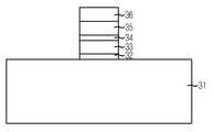
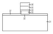
31 : 반도체 기판32 : 게이트 산화막31
33 : 폴리실리콘막34 : 베리어 메탈33: polysilicon film 34: barrier metal
35 : 텅스텐막36 : 게이트 하드마스크35
37 : 게이트 재산화막37: gate property film
본 발명은 반도체 제조 기술에 관한 것으로, 특히 저온 플라즈마 선택적 게이트 재산화 공정을 이용한 반도체 소자 제조 방법에 관한 것이다.BACKGROUND OF THE
일반적으로, 폴리실리콘막(Polysilicon)을 게이트 전극으로 적용하는 반도체 소자 제조에서는 폴리실리콘막 식각시에 게이트 산화막이 손상되므로, 게이트 전극의 저항은 그대로 유지하면서 손상된 게이트 산화막을 회복하기 위해 폴리실리콘막의 측면을 선택적으로 산화시키는 재산화(Re-oxidation) 공정이 수반된다.In general, in the fabrication of a semiconductor device using a polysilicon film as a gate electrode, the gate oxide film is damaged during the etching of the polysilicon film, so that the side of the polysilicon film is recovered to recover the damaged gate oxide film while maintaining the resistance of the gate electrode. A re-oxidation process is involved which selectively oxidizes.
게이트 산화막의 재산화 공정은 게이트 전극 식각시 게이트 산화막에 발생된 마이크로 트렌치 및 손실을 회복시켜주며, 기판에 잔류하는 폴리실리콘막 잔막을 산화시키며, 게이트 전극의 엣지에 있는 게이트 산화막의 두께를 증가시켜서 신뢰성을 향상시키기 위한 목적으로 진행되고 있다.The reoxidation process of the gate oxide film recovers micro trenches and losses generated in the gate oxide film during etching of the gate electrode, oxidizes the remaining polysilicon film remaining on the substrate, and increases the thickness of the gate oxide film at the edge of the gate electrode. It is progressing for the purpose of improving reliability.
한편, 최근에는 게이트 전극의 저항을 낮추기 위해 폴리실리콘막과 금속막의 적층 구조, 즉 폴리메탈 게이트 전극을 사용하고 있다. 예컨대, WSix/poly-Si 구조의 텅스텐 폴리사이드 게이트 전극 및 좀 더 낮은 저항을 갖는 W/WN/poly-Si와 같은 텅스텐 폴리-메탈 게이트 전극 구조를 사용하고 있다.On the other hand, in recent years, in order to lower the resistance of a gate electrode, the laminated structure of a polysilicon film and a metal film, ie, a polymetal gate electrode, is used. For example, a tungsten polyside gate electrode of WSix / poly-Si structure and a tungsten poly-metal gate electrode structure such as W / WN / poly-Si having lower resistance are used.
그러나, 폴리메탈 게이트 전극은 후속 공정 중 높은 열공정 또는 산화 공정에서 급격한 부피 팽창, 시트 저항의 증가 및 폴리실리콘막과 금속막 계면의 반응 등의 문제가 발생한다. 특히, 일정 산화 분위기에서 금속막이 산화되는 것이 공정상 가장 큰 문제로 부각되고 있는데, 이를 극복하기 위한 새로운 공정이 선택적 게이트 재산화(selective gate re-oxidation) 공정이다. 즉, 수소 부화(H2 rich)의 산화 분위기에서 금속막은 산화시키지 않고, 양측벽이 드러난 폴리실리콘막만 산화시키는 공정이다.However, the polymetal gate electrode has problems such as rapid volume expansion, an increase in sheet resistance, and a reaction between the polysilicon film and the metal film interface in a high thermal process or an oxidation process during subsequent processes. In particular, the oxidation of the metal film in a certain oxidizing atmosphere is emerging as the biggest problem in the process, a new process to overcome this is the selective gate re-oxidation process. In other words, the metal film is not oxidized in the hydrogen-enriched (H2 rich) oxidizing atmosphere, but only the polysilicon film in which both side walls are exposed.
도 1a 내지 도 1e는 제 1 종래 기술에 따른 반도체 소자 제조 방법을 도시한 공정 단면도와 그래프이다.1A to 1E are process cross-sectional views and graphs showing a method of manufacturing a semiconductor device according to the first prior art.
도 1a에 도시된 바와 같이, 반도체 기판(11) 상에 게이트 산화막(12)을 형성하고, 게이트 산화막(12) 상에 폴리실리콘막(13), 텅스텐실리사이드막(14), 텅스텐질화막(15), 텅스텐막(16) 및 게이트 하드마스크(17)가 적층 형성된 게이트 패턴을 형성한다.As shown in FIG. 1A, a
한편, 텅스텐실리사이드막(14)과 텅스텐질화막(15)은 폴리실리콘막(13)과 텅스텐막(16)간의 확산 베리어로 사용한다.On the other hand, the
도 1b에 도시된 바와 같이, 게이트 패턴을 형성한 후 850℃ 이상의 온도에서 열처리를 실시하여 게이트 재산화를 실시한다. 이 때, 텅스텐질화막(15)이 고온 열처리에 의해 분해되면서 방출되는 질소(N)가 텅스텐실리사이드막(14)과 반응하여 얇은 W-Si-N막(18)이 형성된다.As shown in FIG. 1B, after the gate pattern is formed, heat treatment is performed at a temperature of 850 ° C. or higher to perform gate reoxidation. At this time, nitrogen (N) released as the
도 1c는, 각종 베리어 메탈에 따른 텅스텐막-폴리실리콘막간의 콘택 저항 및 시트 저항을 나타낸 그래프로서, A는 텅스텐막/텅스텐질화막, B는 텅스텐막/텅스텐 질화막/티타늄나이트라이드막/티타늄막, C는 텅스텐막/텅스텐질화막/텅스텐실리사이드막을 나타낸다.1C is a graph showing contact resistance and sheet resistance between tungsten film and polysilicon film according to various barrier metals, A is tungsten film / tungsten nitride film, B is tungsten film / tungsten nitride film / titanium nitride film / titanium film, C represents a tungsten film / tungsten nitride film / tungsten silicide film.
A는 B와 C에 비해 콘택 저항은 높으나 시트 저항은 비교적 낮고, B는 A와 C에 비해 콘택 저항은 가장 낮으나 시트 저항이 가장 크다. C는 B와 비교하여 콘택 저항은 높지만, A와 C에 비해 상대적으로 낮은 콘택 저항(RC)과 시트 저항(RS)을 모두 얻을 수 있다.A has a higher contact resistance than B and C but a relatively low sheet resistance, and B has the lowest contact resistance compared to A and C but the largest sheet resistance. C has a higher contact resistance than B, but can obtain both a lower contact resistance (RC ) and a sheet resistance (RS ) than A and C.
도 1d는, 텅스텐질화막과 텅스텐질화막/텅스텐실리사이드막을 베리어 메탈로 사용하는 경우 850℃ 이상의 고온 선택적 게이트 재산화(열산화)를 실시할 때, 텅스텐막과 폴리실리콘막간의 콘택 저항에 관한 그래프로서, 다량의 H2 분위기 때문에 텅스텐막의 산화는 방지가 가능하지만, 소량의 산소로 인하여 계면에 존재하는 티타늄나이트라이드막, 티타늄막 및 텅스텐실리콘질화막, 텅스텐실리사이드막과 같은 물질은 산화를 피할 수 없다. 계면이 산화하는 경우, 계면 저항이 매우 높아지는 문제가 발생한다.FIG. 1D is a graph of the contact resistance between the tungsten film and the polysilicon film when the tungsten nitride film and the tungsten nitride film / tungsten silicide film are used as the barrier metal when high temperature selective gate reoxidation (thermal oxidation) of 850 ° C. or more is performed. Oxidation of the tungsten film can be prevented due to a large amount of H2 atmosphere, but oxidation of materials such as titanium nitride film, titanium film and tungsten silicon nitride film, and tungsten silicide film existing at the interface due to a small amount of oxygen is inevitable. When the interface is oxidized, a problem arises in that the interface resistance becomes very high.
도 1e는, 폴리실리콘막과 텅스텐막이 적층 형성된 게이트에 열 선택적 재산화(A')와 플라즈마 선택적 재산화(B') 적용시 계면 산화의 정도를 나타낸 그래프로서, 열산화 적용시 플라즈마 재산화와 비교하여 산소 이온이 텅스텐막의 측벽을 통과하여 계면까지 확산이 가능함을 알 수 있다.FIG. 1E is a graph showing the degree of interfacial oxidation when thermal selective reoxidation (A ') and plasma selective reoxidation (B') are applied to a gate in which a polysilicon film and a tungsten film are laminated. In comparison, it can be seen that oxygen ions pass through the sidewall of the tungsten film and can be diffused to the interface.
상술한 문제를 해결하기 위한 방법으로, 도 2a 및 도 2b는 열 선택적 게이트 재산화 공정에 의한 텅스텐 측벽으로의 산화 침투를 억제하기 위한 제 2 종래 기술 에 따른 반도체 소자 제조 방법을 도시한 공정 단면도와 그래프이다.As a method for solving the above problems, FIGS. 2A and 2B are cross-sectional views showing a method of manufacturing a semiconductor device according to the second prior art for suppressing oxidation penetration into a tungsten sidewall by a thermally selective gate reoxidation process; It is a graph.
도 2a에 도시된 바와 같이, 반도체 기판(21) 상에 게이트 산화막(22), 게이트 전극용 폴리실리콘막(23), 베리어 메탈(24), 텅스텐막(25), 게이트 하드마스크(26)이 적층된 게이트 패턴을 형성한다. 이 때, 게이트 패턴 식각시 폴리실리콘막(23)의 상부 일부까지만 1차 게이트 식각을 진행한다.As shown in FIG. 2A, the
이 때, 베리어 메탈(24)은 텅스텐질화막, 텅스텐질화막/티타늄나이트라이드막/티타늄막, 텅스텐질화막/티타늄막, 텅스텐질화막/텅스텐실리사이드막 및 텅스텐질화막/텅스텐실리콘질화막/텅스텐실리사이드막으로 이루어진 그룹에서 선택된 메탈 구조를 사용한다.At this time, the
계속해서, 텅스텐막(25) 및 베리어 메탈(24)을 캡핑하기 위해 게이트 패턴의 표면을 따라 스페이서 질화막(또는 캡핑 질화막)을 증착한다.Subsequently, a spacer nitride film (or capping nitride film) is deposited along the surface of the gate pattern to cap the
이어서, 스페이서 질화막을 식각하여 게이트 패턴 측벽에 부착된 스페이서(27)를 형성한 후 잔류하는 폴리실리콘막(23)을 완전히 식각하는 2차 게이트 식각을 진행한다.Subsequently, after the spacer nitride layer is etched to form the spacer 27 attached to the gate pattern sidewall, secondary gate etching is performed to completely etch the
다음으로, 850℃ 이상의 H2O/H2 분위기에서 선택적 게이트 재산화 공정을 진행하여 폴리실리콘막(23) 측면 및 게이트 산화막(22) 상에 게이트 재산화막(28)이 형성된다.Next, a selective gate reoxidation process is performed in an H2 O / H2 atmosphere of 850 ° C. or higher to form a gate reoxidation film 28 on the
도 2b를 참조하면, 각종 베리어 메탈(C,D,E)을 갖는 게이트 전극 형성시 스페이서 적용에 따른 자기 정렬 콘택 페일 특성을 나타낸 것으로, 게이트 식각 프로파일 불량이 발생하는 경우 자기 정렬 콘택 특성의 열화가 나타난다.Referring to FIG. 2B, the self-aligned contact fail characteristic according to the spacer application when forming the gate electrode having various barrier metals (C, D, and E) is shown. When the gate etch profile defect occurs, the deterioration of the self-aligned contact characteristic is appear.
그러나, 상술한 바와 같이 스페이서 형성시 열공정에 의해 하부 폴리실리콘막이 폴리 결정(poly-crystallization)이 발생하여 게이트 특성이 저하되며, 게이트 식각 불량이 발생하는 경우 자기 정렬 콘택 특성의 열화와 같은 문제가 있다.However, as described above, when the spacers are formed, the lower polysilicon layer generates poly-crystallization due to a thermal process, thereby deteriorating gate characteristics, and in the case of poor gate etching, problems such as deterioration of self-aligned contact characteristics occur. have.
본 발명은 상기한 종래 기술의 문제점을 해결하기 위해 제안된 것으로, 선택적 게이트 재산화 공정시 메탈막과 폴리실리콘막간의 계면 저항이 높아지는 문제를 방지하는데 적합한 반도체 소자 제조 방법을 제공하는데 그 목적이 있다.The present invention has been proposed to solve the above problems of the prior art, and an object of the present invention is to provide a method for manufacturing a semiconductor device suitable for preventing the problem of increasing the interface resistance between the metal film and the polysilicon film during the selective gate reoxidation process. .
상기 목적을 달성하기 위한 특징적인 본 발명의 반도체 소자 제조 방법은 반도체 기판 상부에 게이트 절연막을 형성하는 단계; 상기 게이트절연막 상에 폴리실리콘막을 형성하는 단계; 상기 폴리실리콘막 상에 적어도 메탈실리사이드막을 포함하는 배리어메탈을 형성하는 단계; 상기 배리어메탈 상에 전도막과 게이트하드마스크를 차례로 형성하는 단계; 상기 게이트 하드마스크, 전도막, 베리어 메탈, 폴리실리콘막 및 게이트 절연막을 패터닝하여 게이트 패턴을 형성하는 단계; 선택적 플라즈마 방식의 게이트 재산화를 실시하는 단계; 및 열처리하는 단계를 포함한다.A semiconductor device manufacturing method of the present invention for achieving the above object comprises the steps of forming a gate insulating film on the semiconductor substrate; Forming a polysilicon film on the gate insulating film; Forming a barrier metal including at least a metal silicide layer on the polysilicon layer; Sequentially forming a conductive film and a gate hard mask on the barrier metal; Patterning the gate hard mask, the conductive layer, the barrier metal, the polysilicon layer, and the gate insulating layer to form a gate pattern; Performing a gate reoxidation of the selective plasma method; And heat treatment.
또한, 본 발명은 반도체 기판 상에 게이트 절연막을 형성하는 단계; 상기 게이트 절연막 상에 폴리실리콘막을 형성하는 단계; 상기 폴리실리콘막 상에 적어도 메탈실리사이드막을 포함하는 베리어 메탈을 형성하는 단계; 상기 베리어 메탈 상에 텅스텐막 및 게이트 하드마스크를 차례로 형성하는 단계; 상기 게이트하드마스크, 텅스텐막, 배리어메탈, 폴리실리콘막 및 게이트절연막을 식각하여 게이트 패턴을 형성하는 단계; 선택적 플라즈마 방식의 게이트 재산화를 실시하는 단계; 및 열처리하는 단계를 포함한다.In addition, the present invention comprises the steps of forming a gate insulating film on a semiconductor substrate; Forming a polysilicon film on the gate insulating film; Forming a barrier metal including at least a metal silicide layer on the polysilicon layer; Sequentially forming a tungsten film and a gate hard mask on the barrier metal; Etching the gate hard mask, the tungsten film, the barrier metal, the polysilicon film, and the gate insulating film to form a gate pattern; Performing a gate reoxidation of the selective plasma method; And heat treatment.
이하, 본 발명이 속하는 기술 분야에서 통상의 지식을 가진 자가 본 발명의 기술적 사상을 용이하게 실시할 수 있을 정도로 상세히 설명하기 위하여, 본 발명의 가장 바람직한 실시예를 첨부 도면을 참조하여 설명하기로 한다.Hereinafter, the most preferred embodiments of the present invention will be described in detail with reference to the accompanying drawings so that those skilled in the art can easily implement the technical idea of the present invention. .
도 3a 및 도 3b는 본 발명의 일실시예에 따른 반도체 소자 제조 방법을 도시한 공정 단면도이다.3A and 3B are cross-sectional views illustrating a method of manufacturing a semiconductor device in accordance with an embodiment of the present invention.
도 3a에 도시된 바와 같이, 웰 형성 공정 및 소자 분리 공정이 진행된 반도체 기판(31) 열산화법으로 반도체 기판(31) 상에 게이트 산화막(32)을 형성한다. 이 때, 게이트 산화막(32)은 20∼100Å의 두께로 형성한다.As shown in FIG. 3A, the
이어서, 게이트 산화막(32) 상에 게이트 전극용 폴리실리콘막(33)을 형성하고, 폴리실리콘막(33) 상에 베리어 메탈(34)을 증착한다.Next, a
이 때, 베리어 메탈(34)은 메탈질화막 또는 메탈실리콘질화막을 사용하는데, 본 발명의 실시예에서는 텅스텐질화막(WN) 또는 텅스텐실리콘질화막(WSiN)을 사용할 수 있다. 그리고, 텅스텐실리콘질화막 외에도 탄탈륨실리콘질화막(TaSiN), 티타늄실리콘질화막(TiSiN), 몰리브덴실리콘질화막(MoSiN), 하프늄실리콘질화막(HfSiN), 지르코늄실리콘질화막(ZrSiN), 코발트실리콘질화막(CoSiN), 크롬실리콘질화막(CrSiN) 및 니켈실리콘질화막(NiSiN)으로 이루어진 그룹에서 선택된 어느 하나의 메탈실리콘질화막을 사용할 수 있다.In this case, the
한편, 본 발명의 실시예에서는 게이트 전극용 전도막으로 폴리실리콘막(33)을 사용하였으나, 폴리실리콘게르마늄(poly-Si(1-x)-Gex(x=0.01∼0.99) 또는 Ni, Cr, Co, Ti, W, Ta 및 Hf이 포함된 실리사이드막으로 이루어진 그룹에서 선택된 물질을 사용할 수 있다.Meanwhile, in the embodiment of the present invention, a
한편, 폴리실리콘막(33) 상에 즉, 폴리실리콘막(33)과 배리어메탈(34) 사이에 다른 배리어메탈로서 텅스텐실리사이드막(도시 생략)이 형성될 수 있으며, 이때 텅스텐실리사이드막은 비정질(amorphous) 물질이며, 20∼200Å의 두께로 형성한다.On the other hand, a tungsten silicide film (not shown) may be formed on the
또한, 텅스텐실리사이드막 외에도 탄탈륨실리사이드(TaSix), 티타늄실리사이드(TiSix), 몰리브덴실리사이드(MoSix), 하프늄실리사이드(HfSix), 지르코늄실리사이드(ZrSix), 코발트실리사이드(CoSix), 크롬실리사이드(CrSix), 및 니켈실리사이드(NiSix)로 이루어진 그룹에서 선택된 물질을 사용할 수 있다.
상술한 바에 따르면, 배리어메탈(34)은 메탈질화막 또는 메탈실리콘질화막을 사용하거나, 또는 메탈실리사이드와 메탈질화막의 적층(메탈질화막/메탈실리사이드), 메탈실리사이드와 메탈실리콘질화막의 적층(메탈실리콘질화막/메탈실리사이드)을 사용할 수 있다.In addition to the tungsten silicide layer, tantalum silicide (TaSix ), titanium silicide (TiSix ), molybdenum silicide (MoSix ), hafnium silicide (HfSix ), zirconium silicide (ZrSix ), cobalt silicide (CoSix ), and chrome silicide Materials selected from the group consisting of (CrSix ), and nickel silicide (NiSix ) may be used.
As described above, the
계속해서, 베리어 메탈(34) 상에 게이트 전극용 전도막으로 텅스텐막(35)을 증착하고, 텅스텐막 상에 게이트하드마스크질화막(36)를 적층 형성한다.Subsequently, a
한편, 게이트 전극용 전도막으로 텅스텐막(35) 외에도 탄탈륨(Ta), 티타늄(Ti), 몰리브덴(Mo), 하프늄(Hf), 지르코늄(Zr), 코발트(Co), 크롬(Cr), 니켈(Ni), 백금(Pt) 및 루테늄(Ru)으로 이루어진 그룹에서 선택된 어느 한 물질을 사용할 수 있다.Meanwhile, in addition to the
계속해서, 게이트하드마스크질화막(36) 상에 포토레지스트 패턴(도시하지 않음)을 형성하고, 포토레지스트 패턴을 사용하여 게이트하드마스크질화막(36)을 식각한 후, 스트립한다.Subsequently, a photoresist pattern (not shown) is formed on the gate hard
이어서, 게이트하드마스크질화막(36)을 식각 베리어로 텅스텐막(35), 베리어 메탈(34), 폴리실리콘막(33), 게이트 산화막(32)을 차례로 패터닝하여 게이트 패턴을 형성한다.Subsequently, a gate pattern is formed by patterning the
도 3b에 도시된 바와 같이, 게이트 패턴이 형성된 결과물의 전면에 플라즈마 방식의 선택적 게이트 재산화(Plasma selective gate reoxidation) 공정을 진행한다.As shown in FIG. 3B, a plasma selective gate reoxidation process is performed on the entire surface of the resultant gate pattern.
게이트 재산화 공정은 게이트 전극용 적층막들을 식각하여 게이트 패턴을 형성한 다음 게이트 산화막에 생긴 마이크로 트렌치 및 플라즈마 데미지를 회복시키기 위함이며, 또한 반도체 기판에 잔류하는 전극 물질을 산화시키고 게이트 엣지(Edge)에 있는 게이트 산화막의 두께를 증가시켜 GGO(Graded Gate oxide)를 형성하므로써, 소자의 신뢰성을 향상시키기 위한 목적으로 실시된다.The gate reoxidation process is to etch the stacked layers for the gate electrode to form a gate pattern, and then to recover the micro trenches and plasma damage caused to the gate oxide layer, and also to oxidize the electrode material remaining on the semiconductor substrate and to gate edge. By increasing the thickness of the gate oxide film in the film to form a GGO (Graded Gate oxide), it is carried out for the purpose of improving the reliability of the device.
한편, 본 발명의 실시예에서 적용하는 플라즈마 방식의 선택적 게이트 재산화 공정시 반도체 기판(31)의 온도는 400∼800℃로 유지하고, 이 때 반응 기체는 산소(O2)/수소(H2) 또는 산소(O2)/듀테륨(D2) 혼합 기체를 사용하도록 한다.On the other hand, the temperature of the
플라즈마 방식의 선택적 게이트 재산화 공정시 플라즈마 발생 장치는 RF(Radio Frequency) 또는 마이크로 웨이브 모두 사용할 수 있다.In the selective gate reoxidation process of the plasma method, the plasma generator may use either RF (Radio Frequency) or microwave.
또한, 플라즈마 방식의 선택적 게이트 재산화 공정시 산화막의 특성을 향상시키기 위해 추가적으로 N2, N2O 또는 진공분위기에서 열처리를 실시할 수 있다.In addition, in order to improve the characteristics of the oxide film during the selective gate reoxidation process of the plasma method, heat treatment may be additionally performed in N2 , N2 O, or a vacuum atmosphere.
도 4a 내지 도 4e는 본 발명을 설명하기 위한 그래프와 TEM 사진이다.4A to 4E are graphs and TEM photographs for explaining the present invention.
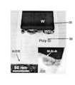
도 4a는 텅스텐막(35)/텅스텐질화막(텅스텐실리콘질화막)/텅스텐실리사이드막(34)/폴리실리콘막(33)이 적층된 게이트 전극의 플라즈마 방식의 선택적 게이트 재산화 공정 후 실제 단면 TEM 사진으로서, 텅스텐질화막(WN)에서 분해되어 나오는 N과 텅스텐실리사이드막(WSix)의 반응에 의해 텅스텐실리사이드막의 상부에 일정 두께의 W-Si-N막이 형성됨을 알 수 있다. 텅스텐실리사이드막 표면에 절연체 특성을 갖으면서도 도전체 특성을 보이는 이러한 W-Si-N 막이 형성되므로, 텅스텐-폴리 게이트 스택의 계면 저항을 감소시킬 수 있다.FIG. 4A is a real cross-sectional TEM photograph after a plasma selective gate reoxidation process of a gate electrode in which a
도 4b는 텅스텐-폴리 게이트 스택의 SIMS 깊이 프로파일(열 선택적 게이트 재산화(F) 대비 플라즈마 방식의 선택적 게이트 재산화(G))을 나타낸 것으로, 열 게이트 선택적 재산화 진행시, 플라즈마 방식의 게이트 재산화 보다 텅스텐막과 폴리실리콘막 계면에 더 많은 산소가 검출됨을 알 수 있다.FIG. 4B shows the SIMS depth profile of the tungsten-poly gate stack (plasma selective gate regeneration (G) vs. thermal selective gate reoxidation (F)), with the plasma gate properties during the thermal gate selective reoxidation. It can be seen that more oxygen is detected at the interface between the tungsten film and the polysilicon film than the oxidation.
결국, 플라즈마 방식의 선택적 게이트 재산화를 진행하면 텅스텐-폴리 게이트 스택의 계면에 적은 산소량이 검출됨을 알 수 있다.As a result, when the selective gate reoxidation of the plasma method is performed, it can be seen that a small amount of oxygen is detected at the interface of the tungsten-poly gate stack.
도 4c은 각종 텅스텐-폴리 게이트 스택 구조의 열 선택적 게이트 재산화 및 플라즈마 방식의 선택적 게이트 재산화에 따른 QBD(Charge to Breakdown) 특성을 나타낸 그래프로서, (A")는 폴리실리콘막, 텅스텐질화막, 텅스텐막이 적층된 구조이며 열 게이트 선택적 산화를 나타낸 것이며, (B")는 폴리실리콘막, 텅스텐질화막, 텅스텐막이 적층된 구조이며, 프리 스페이서를 적용한 열 게이트 선택적 산화를 나타낸 것이며, (C")는 폴리실리콘막, 텅스텐질화막, 텅스텐막이 적층된 구조이며, 플라즈마 선택적 게이트 산화를 나타낸 것이며, (D")는 폴리실리콘막, 텅스텐실리사이드막, 텅스텐질화막, 텅스텐막이 적층된 구조이며, 프리 스페이서를 적용한 열 게이트 선택적 산화를 나타낸 것이며, (E")는 폴리실리콘막, 텅스텐실리사이드막, 텅스텐질화막, 텅스텐막이 적층된 구조이며, 플라즈마 선택적 게이트 산화를 나타낸 것이다.4C is a graph showing QBD (Charge to Breakdown) characteristics according to thermal selective gate reoxidation of various tungsten-poly gate stack structures and selective gate recrystallization of plasma method. Tungsten film is a stacked structure and shows thermal gate selective oxidation, (B ") is a structure in which a polysilicon film, tungsten nitride film, and tungsten film is stacked, and heat gate selective oxidation is applied with pre-spacer, and (C") is Polysilicon film, tungsten nitride film, and tungsten film are laminated, and plasma selective gate oxidation is shown. (D ″) is a structure in which polysilicon film, tungsten silicide film, tungsten nitride film, and tungsten film are stacked, The gate selective oxidation is shown, and (E ") is a polysilicon film, a tungsten silicide film, a tungsten nitride film, and a tungsten film laminated. Structure, and it shows the plasma selective gate oxide.
그래프를 살펴보면, 텅스텐질화막/텅스텐실리사이드막을 베리어 메탈로 플라즈마 방식의 선택적 게이트 재산화(E")를 실시하는 경우, 텅스텐질화막을 베리어 메탈로 사용하면서 열 게이트 재산화(A")를 실시할 때와 대비하여 QBD 특성이 향상됨을 알 수 있다.In the graph, when the tungsten nitride film / tungsten silicide film is subjected to plasma gate selective gate reoxidation (E ″) with barrier metal, the thermal gate reoxidation (A ″) using tungsten nitride film as barrier metal is performed. In contrast, it can be seen that QBD characteristics are improved.
이러한, QBD 특성은 텅스텐실리사이드막이 후속 열공정시 게이트하드마스크질화막의 기계적 스트레스를 완충시켜주는 버퍼 역할을 하여 게이트 산화막의 신뢰성을 향상시킨다.This QBD characteristic improves the reliability of the gate oxide film by acting as a buffer to buffer the mechanical stress of the gate hard mask nitride film during the subsequent thermal process.
따라서, 베리어 메탈로 텅스텐질화막만을 사용할 때보다 텅스텐실리사이드막을 함께 사용하는 것이 QBD 특성이 좋다는 것을 알 수 있으며, 베리어 메탈로 텅스텐질화막을 사용하면 열 선택적 게이트 재산화에 비해, 스페이서 열산화가 QBD가 좋고 스페이서 열산화에 비해 플라즈마 방식의 선택적 게이트 재산화의 QBD 특성이 좋은 것을 알 수 있다.Therefore, it can be seen that the use of tungsten silicide layer together with the tungsten silicide layer is better than the barrier metal as the tungsten nitride layer, and the use of the barrier metal as tungsten nitride layer has better QBD than the thermal selective gate reoxidation. It can be seen that the QBD characteristics of the selective gate reoxidation of the plasma method are better than the spacer thermal oxidation.
또한, 베리어 메탈로 텅스텐질화막과 텅스텐실리사이드를 사용할 때는 스페이서 열산화에 비해 플라즈마 방식의 선택적 게이트 재산화의 QBD 특성이 좋은 것을 알 수 있다.In addition, when the tungsten nitride film and tungsten silicide are used as the barrier metal, it can be seen that the QBD characteristics of the selective gate reoxidation of the plasma method are better than the spacer thermal oxidation.
따라서, 800℃ 이하의 저온 플라즈마 방식의 선택적 게이트 재산화를 진행하면, 수소에 의한 게이트 산화막 특성 열화가 상대적으로 감소하기 때문에 열 선택적 게이트 재산화 시보다 우수한 QBD 특성을 얻을 수 있다.Therefore, when the selective gate reoxidation of the low-temperature plasma method of 800 ° C. or less proceeds, the gate oxide film characteristic deterioration due to hydrogen is relatively reduced, thereby obtaining better QBD characteristics than the thermal selective gate regeneration.
도 4d는 각종 베리어 메탈 및 게이트 선택적 재산화 방법에 따른 게이트 산화막 스트레스 유도 누설 전류(Stress Induced Leakage Current; SILC 'H') 및 스트레스 후 인터페이스 트랩 밀도(Interface Trap Density; DIT 'I') 특성을 나타낸 그래프로서, 점선을 기준으로 왼쪽의 열 선택적 게이트 재산화와 오른쪽의 플라즈마 방식의 선택적 재산화를 비교하여 보면, 텅스텐질화막/텅스텐실리사이드막을 베리어 메탈로 사용하면서 플라즈마 방식의 선택적 게이트 재산화를 진행하면, 열 선택적 게이트 재산화를 실시한 후의 값과 비교하여 SILC 및 스트레스 후 DIT 특성이 향상됨을 알 수 있다.4D illustrates the characteristics of gate oxide stress induced leakage current (SILC 'H') and interface trap density (DIT 'I') after stress according to various barrier metal and gate selective reoxidation methods. As a graph, comparing the selective column recrystallization of the left column with the selective recrystallization of the plasma method on the right, when the tungsten nitride film / tungsten silicide film is used as the barrier metal, the selective gate reoxidation of the plasma method is performed. It can be seen that the SILC and post-stress DIT characteristics are improved compared to the values after thermal selective gate reoxidation.
도 4e는, 게이트 선택적 재산화 방법에 따른 DRAM에서의 어레이 셀 트랜지스터의 셀 접합 누설 특성을 나타낸 그래프로서, 열 선택적 게이트 재산화 대비 플라즈마 방식의 선택적 게이트 재산화를 적용하면, 드레인 전압 및 전류의 저영역(low field) 및 고영역(high field)에서의 셀 접합 누설 및 게이트 유도 드레인 누설(Gate Induced Drain Leakage; GIDL) 특성이 모두 향상되어 소자의 동작 특성이 개선됨을 알 수 있다.4E is a graph showing cell junction leakage characteristics of an array cell transistor in a DRAM according to a gate selective reoxidation method. It can be seen that the cell junction leakage and gate induced drain leakage (GIDL) characteristics in both the low and high fields are improved to improve the operation characteristics of the device.
상술한 바와 같이, 베리어 메탈로 텅스텐질화막 하부에 텅스텐실리사이드막을 삽입하고, 저온 플라즈마 방식의 선택적 게이트 재산화에 의해 QBD 특성이 향상됨을 알 수 있다.As described above, it is seen that the QBD characteristics are improved by inserting a tungsten silicide film under the tungsten nitride film with the barrier metal and selective gate reoxidation using a low temperature plasma method.
한편, 본 발명은 텅스텐-폴리메탈 구조로 이루어진 게이트 전극 이외에도, 텅스텐실리사이드/폴리실리콘 및 티타늄실리사이드/폴리실리콘/니켈실리사이드, 폴리실리콘, 크롬실리사이드/폴리실리콘, 코발트실리사이드/폴리실리콘, 하프늄실리사이드/폴리실리콘 구조의 게이트 전극에도 적용이 가능하다.On the other hand, the present invention, in addition to the gate electrode made of a tungsten-polymetal structure, tungsten silicide / polysilicon and titanium silicide / polysilicon / nickel silicide, polysilicon, chrome silicide / polysilicon, cobalt silicide / polysilicon, hafnium silicide / poly It is also applicable to the gate electrode of the silicon structure.
또한, 본 발명은 텅스텐질화막(WN), 티타늄질화막(TiN), 루테늄탄탈륨질화막(RuTaN), 루테늄질화막(RuN), 루테늄(Ru)과 같은 다이렉트 메탈 게이트 전극에도 적용 가능하다.The present invention is also applicable to direct metal gate electrodes such as tungsten nitride film (WN), titanium nitride film (TiN), ruthenium tantalum nitride film (RuTaN), ruthenium nitride film (RuN), and ruthenium (Ru).
본 발명의 기술 사상은 상기 바람직한 실시예에 따라 구체적으로 기술되었으나, 상기한 실시예는 그 설명을 위한 것이며 그 제한을 위한 것이 아님을 주의하여야 한다. 또한, 본 발명의 기술 분야의 통상의 전문가라면 본 발명의 기술 사상의 범위 내에서 다양한 실시예가 가능함을 이해할 수 있을 것이다.Although the technical idea of the present invention has been described in detail according to the above preferred embodiment, it should be noted that the above-described embodiment is for the purpose of description and not of limitation. In addition, those skilled in the art will understand that various embodiments are possible within the scope of the technical idea of the present invention.
상술한 본 발명은 WN/TiN/Ti, WN/Ti, WN/WSix 및 WN/WSiN/WSix와 같은 확산 베리어 메탈을 갖는 텅스텐 폴리메탈 게이트 구조를 갖는 반도체 소자에 플라즈마 선택적 게이트 재산화 공정을 적용하여 텅스텐막과 베리어 메탈 간의 계면 산화를 억제함으로써, 고속 동작이 가능한 CMOSFET 소자 및 메모리 소자를 제작할 수 있다.The present invention described above provides a plasma selective gate reoxidation process for a semiconductor device having a tungsten polymetal gate structure having a diffusion barrier metal such as WN / TiN / Ti, WN / Ti, WN / WSix and WN / WSiN / WSix . By suppressing the interfacial oxidation between the tungsten film and the barrier metal, the CMOSFET device and the memory device capable of high-speed operation can be manufactured.
또한, 본 발명은 수소에 의한 게이트 산화막의 열화가 약하기 때문에, 게이트 산화막의 신뢰성이 크게 되는 효과가 있다.In addition, since the deterioration of the gate oxide film by hydrogen is weak, the present invention has the effect of increasing the reliability of the gate oxide film.
또한, 본 발명은 플라즈마 선택적 게이트 재산화 공정시 저온(800℃ 이하) 효과에 의해 메모리 소자의 셀 트랜지스터에서 접합 누설 특성이 향상되는 효과가 있다.In addition, the present invention has the effect of improving the junction leakage characteristics in the cell transistor of the memory device by the low temperature (800 ℃ or less) effect during the plasma selective gate reoxidation process.
또한, 본 발명은 접합 누설 특성이 향상됨으로써, 메모리 디바이스의 데이타 리텐션 타임이 개선되는 효과가 있다.In addition, the present invention has the effect of improving the data retention time of the memory device by improving the junction leakage characteristic.
Claims (20)
Translated fromKoreanPriority Applications (2)
| Application Number | Priority Date | Filing Date | Title |
|---|---|---|---|
| KR1020050088344AKR100689679B1 (en) | 2005-09-22 | 2005-09-22 | Semiconductor device manufacturing method |
| US11/448,678US7687389B2 (en) | 2005-09-22 | 2006-06-08 | Method for fabricating semiconductor device |
Applications Claiming Priority (1)
| Application Number | Priority Date | Filing Date | Title |
|---|---|---|---|
| KR1020050088344AKR100689679B1 (en) | 2005-09-22 | 2005-09-22 | Semiconductor device manufacturing method |
Publications (1)
| Publication Number | Publication Date |
|---|---|
| KR100689679B1true KR100689679B1 (en) | 2007-03-09 |
Family
ID=37884724
Family Applications (1)
| Application Number | Title | Priority Date | Filing Date |
|---|---|---|---|
| KR1020050088344AExpired - LifetimeKR100689679B1 (en) | 2005-09-22 | 2005-09-22 | Semiconductor device manufacturing method |
Country Status (2)
| Country | Link |
|---|---|
| US (1) | US7687389B2 (en) |
| KR (1) | KR100689679B1 (en) |
Cited By (1)
| Publication number | Priority date | Publication date | Assignee | Title |
|---|---|---|---|---|
| KR20190051082A (en)* | 2016-10-03 | 2019-05-14 | 어플라이드 머티어리얼스, 인코포레이티드 | Methods and devices using PVD ruthenium |
Families Citing this family (11)
| Publication number | Priority date | Publication date | Assignee | Title |
|---|---|---|---|---|
| KR100583609B1 (en)* | 2004-07-05 | 2006-05-26 | 삼성전자주식회사 | Method for manufacturing gate structure of semiconductor device and method for manufacturing cell gate structure of nonvolatile memory device using same |
| DE102007045074B4 (en) | 2006-12-27 | 2009-06-18 | Hynix Semiconductor Inc., Ichon | Semiconductor device with gate stack structure |
| KR100946024B1 (en)* | 2007-09-06 | 2010-03-09 | 주식회사 하이닉스반도체 | Metal wiring of semiconductor devices and method of forming the same |
| US7947561B2 (en)* | 2008-03-14 | 2011-05-24 | Applied Materials, Inc. | Methods for oxidation of a semiconductor device |
| US20090311877A1 (en)* | 2008-06-14 | 2009-12-17 | Applied Materials, Inc. | Post oxidation annealing of low temperature thermal or plasma based oxidation |
| US20100297854A1 (en)* | 2009-04-22 | 2010-11-25 | Applied Materials, Inc. | High throughput selective oxidation of silicon and polysilicon using plasma at room temperature |
| WO2011097178A2 (en)* | 2010-02-02 | 2011-08-11 | Applied Materials, Inc. | Methods for nitridation and oxidation |
| CN104106128B (en) | 2012-02-13 | 2016-11-09 | 应用材料公司 | Method and apparatus for selective oxidation of substrates |
| KR20130116099A (en)* | 2012-04-13 | 2013-10-23 | 삼성전자주식회사 | Semiconductor device and method for fabricating the same |
| US9401279B2 (en) | 2013-06-14 | 2016-07-26 | Sandisk Technologies Llc | Transistor gate and process for making transistor gate |
| US10204960B2 (en)* | 2015-09-17 | 2019-02-12 | Taiwan Semiconductor Manufacturing Co., Ltd. | Method of forming polysilicon gate structure in image sensor device |
Citations (1)
| Publication number | Priority date | Publication date | Assignee | Title |
|---|---|---|---|---|
| JP2000332245A (en)* | 1999-05-25 | 2000-11-30 | Sony Corp | MANUFACTURE OF SEMICONDUCTOR DEVICE AND MANUFACTURE OF p-TYPE SEMICONDUCTOR ELEMENT |
Family Cites Families (6)
| Publication number | Priority date | Publication date | Assignee | Title |
|---|---|---|---|---|
| TW477004B (en)* | 1998-10-12 | 2002-02-21 | United Microelectronics Corp | Method to prevent dopant diffusion in dual-gate |
| KR100351907B1 (en)* | 2000-11-17 | 2002-09-12 | 주식회사 하이닉스반도체 | method for forming gate electrode semiconductor device |
| KR100871465B1 (en)* | 2003-02-13 | 2008-12-03 | 도쿄엘렉트론가부시키가이샤 | Method for manufacturing semiconductor device and forming silicon oxide film, and apparatus for manufacturing semiconductor device |
| US6987056B2 (en)* | 2003-07-08 | 2006-01-17 | Hynix Semiconductor Inc. | Method of forming gates in semiconductor devices |
| JP4191000B2 (en)* | 2003-10-06 | 2008-12-03 | エルピーダメモリ株式会社 | Semiconductor device and manufacturing method thereof |
| US6943416B2 (en)* | 2003-11-20 | 2005-09-13 | Micron Technology, Inc. | Method and structure for reducing resistance of a semiconductor device feature |
- 2005
- 2005-09-22KRKR1020050088344Apatent/KR100689679B1/ennot_activeExpired - Lifetime
- 2006
- 2006-06-08USUS11/448,678patent/US7687389B2/enactiveActive
Patent Citations (1)
| Publication number | Priority date | Publication date | Assignee | Title |
|---|---|---|---|---|
| JP2000332245A (en)* | 1999-05-25 | 2000-11-30 | Sony Corp | MANUFACTURE OF SEMICONDUCTOR DEVICE AND MANUFACTURE OF p-TYPE SEMICONDUCTOR ELEMENT |
Cited By (2)
| Publication number | Priority date | Publication date | Assignee | Title |
|---|---|---|---|---|
| KR20190051082A (en)* | 2016-10-03 | 2019-05-14 | 어플라이드 머티어리얼스, 인코포레이티드 | Methods and devices using PVD ruthenium |
| KR102285299B1 (en)* | 2016-10-03 | 2021-08-02 | 어플라이드 머티어리얼스, 인코포레이티드 | How to form a membrane stack |
Also Published As
| Publication number | Publication date |
|---|---|
| US20070066013A1 (en) | 2007-03-22 |
| US7687389B2 (en) | 2010-03-30 |
Similar Documents
| Publication | Publication Date | Title |
|---|---|---|
| US7687389B2 (en) | Method for fabricating semiconductor device | |
| JP5604540B2 (en) | Method for manufacturing semiconductor device having polymetal gate electrode | |
| US20110186920A1 (en) | Semiconductor device with gate stack structure | |
| KR100471407B1 (en) | Method for fabricating transistor with polymetal gate electrode | |
| US6987056B2 (en) | Method of forming gates in semiconductor devices | |
| KR100543207B1 (en) | Method for manufacturing gate electrode of semiconductor device using hard mask | |
| US20060163671A1 (en) | Silicide cap structure and process for reduced stress and improved gate sheet resistance | |
| US20080211039A1 (en) | Nonvolatile memory devices having metal silicide nanocrystals, methods of forming metal silicide nanocrystals, and methods of forming nonvolatile memory devices having metal silicide nanocrystals | |
| KR100681211B1 (en) | Gate electrode having a double diffusion barrier and method of manufacturing a semiconductor device having the same | |
| JP2002289849A (en) | Semiconductor device and manufacturing method thereof | |
| KR100683488B1 (en) | Polymetal gate electrode and manufacturing method thereof | |
| KR101062835B1 (en) | Method for manufacturing gate electrode of semiconductor device using double hard mask | |
| KR100456316B1 (en) | Method for forming gate in semiconductor device | |
| KR100558045B1 (en) | Semiconductor device having a tungsten polymetal gate including a diffusion barrier and a method of manufacturing the same | |
| KR20050062140A (en) | Gate electrode in semiconductor device and fabricating method thereof | |
| KR100625814B1 (en) | Semiconductor device and manufacturing method thereof | |
| KR100806136B1 (en) | Method of manufacturing semiconductor device with metal gate electrode | |
| KR100806138B1 (en) | Method of manufacturing semiconductor device with metal gate electrode | |
| KR100881736B1 (en) | Manufacturing method of semiconductor device | |
| KR100541371B1 (en) | Stress-Relieved Polymetal Gate Electrode and Manufacturing Method Thereof | |
| KR100806135B1 (en) | Method for manufacturing a semiconductor device having a metal gate electrode | |
| KR100844929B1 (en) | Method of manufacturing semiconductor device with metal gate electrode | |
| KR100438674B1 (en) | Method for semiconductor device with metal-gate electrode using selective oxidation | |
| KR100630769B1 (en) | Semiconductor device and manufacturing method thereof | |
| KR100937992B1 (en) | Gate electrode and manufacturing method of semiconductor device having same |
Legal Events
| Date | Code | Title | Description |
|---|---|---|---|
| A201 | Request for examination | ||
| PA0109 | Patent application | Patent event code:PA01091R01D Comment text:Patent Application Patent event date:20050922 | |
| PA0201 | Request for examination | ||
| E902 | Notification of reason for refusal | ||
| PE0902 | Notice of grounds for rejection | Comment text:Notification of reason for refusal Patent event date:20060828 Patent event code:PE09021S01D | |
| E701 | Decision to grant or registration of patent right | ||
| PE0701 | Decision of registration | Patent event code:PE07011S01D Comment text:Decision to Grant Registration Patent event date:20070119 | |
| GRNT | Written decision to grant | ||
| PR0701 | Registration of establishment | Comment text:Registration of Establishment Patent event date:20070226 Patent event code:PR07011E01D | |
| PR1002 | Payment of registration fee | Payment date:20070227 End annual number:3 Start annual number:1 | |
| PG1601 | Publication of registration | ||
| PR1001 | Payment of annual fee | Payment date:20100126 Start annual number:4 End annual number:4 | |
| PR1001 | Payment of annual fee | Payment date:20110126 Start annual number:5 End annual number:5 | |
| PR1001 | Payment of annual fee | Payment date:20120126 Start annual number:6 End annual number:6 | |
| FPAY | Annual fee payment | Payment date:20130128 Year of fee payment:7 | |
| PR1001 | Payment of annual fee | Payment date:20130128 Start annual number:7 End annual number:7 | |
| FPAY | Annual fee payment | Payment date:20140122 Year of fee payment:8 | |
| PR1001 | Payment of annual fee | Payment date:20140122 Start annual number:8 End annual number:8 | |
| FPAY | Annual fee payment | Payment date:20150121 Year of fee payment:9 | |
| PR1001 | Payment of annual fee | Payment date:20150121 Start annual number:9 End annual number:9 | |
| FPAY | Annual fee payment | Payment date:20160121 Year of fee payment:10 | |
| PR1001 | Payment of annual fee | Payment date:20160121 Start annual number:10 End annual number:10 | |
| FPAY | Annual fee payment | Payment date:20170124 Year of fee payment:11 | |
| PR1001 | Payment of annual fee | Payment date:20170124 Start annual number:11 End annual number:11 | |
| FPAY | Annual fee payment | Payment date:20180122 Year of fee payment:12 | |
| PR1001 | Payment of annual fee | Payment date:20180122 Start annual number:12 End annual number:12 | |
| PR1001 | Payment of annual fee | Payment date:20210126 Start annual number:15 End annual number:15 | |
| PR1001 | Payment of annual fee | Payment date:20220125 Start annual number:16 End annual number:16 | |
| PR1001 | Payment of annual fee | Payment date:20230126 Start annual number:17 End annual number:17 | |
| PR1001 | Payment of annual fee | Payment date:20240124 Start annual number:18 End annual number:18 |