KR100687153B1 - Semiconductor device and manufacturing method thereof - Google Patents
Semiconductor device and manufacturing method thereofDownload PDFInfo
- Publication number
- KR100687153B1 KR100687153B1KR1020040012553AKR20040012553AKR100687153B1KR 100687153 B1KR100687153 B1KR 100687153B1KR 1020040012553 AKR1020040012553 AKR 1020040012553AKR 20040012553 AKR20040012553 AKR 20040012553AKR 100687153 B1KR100687153 B1KR 100687153B1
- Authority
- KR
- South Korea
- Prior art keywords
- layer
- metal
- nitrogen
- layer region
- concentration
- Prior art date
- Legal status (The legal status is an assumption and is not a legal conclusion. Google has not performed a legal analysis and makes no representation as to the accuracy of the status listed.)
- Expired - Fee Related
Links
Images


Classifications
- H—ELECTRICITY
- H01—ELECTRIC ELEMENTS
- H01L—SEMICONDUCTOR DEVICES NOT COVERED BY CLASS H10
- H01L21/00—Processes or apparatus adapted for the manufacture or treatment of semiconductor or solid state devices or of parts thereof
- H01L21/02—Manufacture or treatment of semiconductor devices or of parts thereof
- H01L21/04—Manufacture or treatment of semiconductor devices or of parts thereof the devices having potential barriers, e.g. a PN junction, depletion layer or carrier concentration layer
- H01L21/18—Manufacture or treatment of semiconductor devices or of parts thereof the devices having potential barriers, e.g. a PN junction, depletion layer or carrier concentration layer the devices having semiconductor bodies comprising elements of Group IV of the Periodic Table or AIIIBV compounds with or without impurities, e.g. doping materials
- H01L21/28—Manufacture of electrodes on semiconductor bodies using processes or apparatus not provided for in groups H01L21/20 - H01L21/268
- H01L21/28008—Making conductor-insulator-semiconductor electrodes
- H01L21/28017—Making conductor-insulator-semiconductor electrodes the insulator being formed after the semiconductor body, the semiconductor being silicon
- H01L21/28158—Making the insulator
- H01L21/28167—Making the insulator on single crystalline silicon, e.g. using a liquid, i.e. chemical oxidation
- H01L21/28185—Making the insulator on single crystalline silicon, e.g. using a liquid, i.e. chemical oxidation with a treatment, e.g. annealing, after the formation of the gate insulator and before the formation of the definitive gate conductor
- H—ELECTRICITY
- H10—SEMICONDUCTOR DEVICES; ELECTRIC SOLID-STATE DEVICES NOT OTHERWISE PROVIDED FOR
- H10D—INORGANIC ELECTRIC SEMICONDUCTOR DEVICES
- H10D30/00—Field-effect transistors [FET]
- H10D30/01—Manufacture or treatment
- H10D30/021—Manufacture or treatment of FETs having insulated gates [IGFET]
- H—ELECTRICITY
- H01—ELECTRIC ELEMENTS
- H01L—SEMICONDUCTOR DEVICES NOT COVERED BY CLASS H10
- H01L21/00—Processes or apparatus adapted for the manufacture or treatment of semiconductor or solid state devices or of parts thereof
- H01L21/02—Manufacture or treatment of semiconductor devices or of parts thereof
- H01L21/02104—Forming layers
- H01L21/02107—Forming insulating materials on a substrate
- H01L21/02296—Forming insulating materials on a substrate characterised by the treatment performed before or after the formation of the layer
- H01L21/02318—Forming insulating materials on a substrate characterised by the treatment performed before or after the formation of the layer post-treatment
- H01L21/02321—Forming insulating materials on a substrate characterised by the treatment performed before or after the formation of the layer post-treatment introduction of substances into an already existing insulating layer
- H01L21/02329—Forming insulating materials on a substrate characterised by the treatment performed before or after the formation of the layer post-treatment introduction of substances into an already existing insulating layer introduction of nitrogen
- H—ELECTRICITY
- H01—ELECTRIC ELEMENTS
- H01L—SEMICONDUCTOR DEVICES NOT COVERED BY CLASS H10
- H01L21/00—Processes or apparatus adapted for the manufacture or treatment of semiconductor or solid state devices or of parts thereof
- H01L21/02—Manufacture or treatment of semiconductor devices or of parts thereof
- H01L21/04—Manufacture or treatment of semiconductor devices or of parts thereof the devices having potential barriers, e.g. a PN junction, depletion layer or carrier concentration layer
- H01L21/18—Manufacture or treatment of semiconductor devices or of parts thereof the devices having potential barriers, e.g. a PN junction, depletion layer or carrier concentration layer the devices having semiconductor bodies comprising elements of Group IV of the Periodic Table or AIIIBV compounds with or without impurities, e.g. doping materials
- H01L21/28—Manufacture of electrodes on semiconductor bodies using processes or apparatus not provided for in groups H01L21/20 - H01L21/268
- H01L21/28008—Making conductor-insulator-semiconductor electrodes
- H01L21/28017—Making conductor-insulator-semiconductor electrodes the insulator being formed after the semiconductor body, the semiconductor being silicon
- H01L21/28158—Making the insulator
- H01L21/28167—Making the insulator on single crystalline silicon, e.g. using a liquid, i.e. chemical oxidation
- H01L21/28202—Making the insulator on single crystalline silicon, e.g. using a liquid, i.e. chemical oxidation in a nitrogen-containing ambient, e.g. nitride deposition, growth, oxynitridation, NH3 nitridation, N2O oxidation, thermal nitridation, RTN, plasma nitridation, RPN
- H—ELECTRICITY
- H10—SEMICONDUCTOR DEVICES; ELECTRIC SOLID-STATE DEVICES NOT OTHERWISE PROVIDED FOR
- H10D—INORGANIC ELECTRIC SEMICONDUCTOR DEVICES
- H10D64/00—Electrodes of devices having potential barriers
- H10D64/20—Electrodes characterised by their shapes, relative sizes or dispositions
- H10D64/23—Electrodes carrying the current to be rectified, amplified, oscillated or switched, e.g. sources, drains, anodes or cathodes
- H10D64/251—Source or drain electrodes for field-effect devices
- H—ELECTRICITY
- H10—SEMICONDUCTOR DEVICES; ELECTRIC SOLID-STATE DEVICES NOT OTHERWISE PROVIDED FOR
- H10D—INORGANIC ELECTRIC SEMICONDUCTOR DEVICES
- H10D64/00—Electrodes of devices having potential barriers
- H10D64/20—Electrodes characterised by their shapes, relative sizes or dispositions
- H10D64/27—Electrodes not carrying the current to be rectified, amplified, oscillated or switched, e.g. gates
- H10D64/311—Gate electrodes for field-effect devices
- H10D64/411—Gate electrodes for field-effect devices for FETs
- H10D64/511—Gate electrodes for field-effect devices for FETs for IGFETs
- H—ELECTRICITY
- H10—SEMICONDUCTOR DEVICES; ELECTRIC SOLID-STATE DEVICES NOT OTHERWISE PROVIDED FOR
- H10D—INORGANIC ELECTRIC SEMICONDUCTOR DEVICES
- H10D64/00—Electrodes of devices having potential barriers
- H10D64/60—Electrodes characterised by their materials
- H10D64/66—Electrodes having a conductor capacitively coupled to a semiconductor by an insulator, e.g. MIS electrodes
- H10D64/68—Electrodes having a conductor capacitively coupled to a semiconductor by an insulator, e.g. MIS electrodes characterised by the insulator, e.g. by the gate insulator
- H10D64/681—Electrodes having a conductor capacitively coupled to a semiconductor by an insulator, e.g. MIS electrodes characterised by the insulator, e.g. by the gate insulator having a compositional variation, e.g. multilayered
- H10D64/685—Electrodes having a conductor capacitively coupled to a semiconductor by an insulator, e.g. MIS electrodes characterised by the insulator, e.g. by the gate insulator having a compositional variation, e.g. multilayered being perpendicular to the channel plane
- H—ELECTRICITY
- H10—SEMICONDUCTOR DEVICES; ELECTRIC SOLID-STATE DEVICES NOT OTHERWISE PROVIDED FOR
- H10D—INORGANIC ELECTRIC SEMICONDUCTOR DEVICES
- H10D64/00—Electrodes of devices having potential barriers
- H10D64/60—Electrodes characterised by their materials
- H10D64/66—Electrodes having a conductor capacitively coupled to a semiconductor by an insulator, e.g. MIS electrodes
- H10D64/68—Electrodes having a conductor capacitively coupled to a semiconductor by an insulator, e.g. MIS electrodes characterised by the insulator, e.g. by the gate insulator
- H10D64/691—Electrodes having a conductor capacitively coupled to a semiconductor by an insulator, e.g. MIS electrodes characterised by the insulator, e.g. by the gate insulator comprising metallic compounds, e.g. metal oxides or metal silicates
- H—ELECTRICITY
- H10—SEMICONDUCTOR DEVICES; ELECTRIC SOLID-STATE DEVICES NOT OTHERWISE PROVIDED FOR
- H10D—INORGANIC ELECTRIC SEMICONDUCTOR DEVICES
- H10D64/00—Electrodes of devices having potential barriers
- H10D64/60—Electrodes characterised by their materials
- H10D64/66—Electrodes having a conductor capacitively coupled to a semiconductor by an insulator, e.g. MIS electrodes
- H10D64/68—Electrodes having a conductor capacitively coupled to a semiconductor by an insulator, e.g. MIS electrodes characterised by the insulator, e.g. by the gate insulator
- H10D64/693—Electrodes having a conductor capacitively coupled to a semiconductor by an insulator, e.g. MIS electrodes characterised by the insulator, e.g. by the gate insulator the insulator comprising nitrogen, e.g. nitrides, oxynitrides or nitrogen-doped materials
- H—ELECTRICITY
- H01—ELECTRIC ELEMENTS
- H01L—SEMICONDUCTOR DEVICES NOT COVERED BY CLASS H10
- H01L21/00—Processes or apparatus adapted for the manufacture or treatment of semiconductor or solid state devices or of parts thereof
- H01L21/02—Manufacture or treatment of semiconductor devices or of parts thereof
- H01L21/04—Manufacture or treatment of semiconductor devices or of parts thereof the devices having potential barriers, e.g. a PN junction, depletion layer or carrier concentration layer
- H01L21/18—Manufacture or treatment of semiconductor devices or of parts thereof the devices having potential barriers, e.g. a PN junction, depletion layer or carrier concentration layer the devices having semiconductor bodies comprising elements of Group IV of the Periodic Table or AIIIBV compounds with or without impurities, e.g. doping materials
- H01L21/28—Manufacture of electrodes on semiconductor bodies using processes or apparatus not provided for in groups H01L21/20 - H01L21/268
- H01L21/28008—Making conductor-insulator-semiconductor electrodes
- H01L21/28017—Making conductor-insulator-semiconductor electrodes the insulator being formed after the semiconductor body, the semiconductor being silicon
- H01L21/28158—Making the insulator
- H01L21/28167—Making the insulator on single crystalline silicon, e.g. using a liquid, i.e. chemical oxidation
- H01L21/28194—Making the insulator on single crystalline silicon, e.g. using a liquid, i.e. chemical oxidation by deposition, e.g. evaporation, ALD, CVD, sputtering, laser deposition
Landscapes
- Engineering & Computer Science (AREA)
- Manufacturing & Machinery (AREA)
- Power Engineering (AREA)
- Microelectronics & Electronic Packaging (AREA)
- Physics & Mathematics (AREA)
- Computer Hardware Design (AREA)
- Condensed Matter Physics & Semiconductors (AREA)
- General Physics & Mathematics (AREA)
- Chemical Kinetics & Catalysis (AREA)
- Crystallography & Structural Chemistry (AREA)
- General Chemical & Material Sciences (AREA)
- Chemical & Material Sciences (AREA)
- Insulated Gate Type Field-Effect Transistor (AREA)
- Chemical Vapour Deposition (AREA)
- Formation Of Insulating Films (AREA)
- Physical Vapour Deposition (AREA)
Abstract
Translated fromKoreanDescription
Translated fromKorean도 1은 본 발명의 제1 실시의 형태에 따른 반도체 장치의 제조 방법을 설명하기 위한 단면 모식도.BRIEF DESCRIPTION OF THE DRAWINGS The cross-sectional schematic diagram for demonstrating the manufacturing method of the semiconductor device which concerns on 1st Embodiment of this invention.
도 2는 본 발명의 제1 실시의 형태에 따른 반도체 장치의 제조 방법을 설명하기 위한 농도 분포도.2 is a concentration distribution diagram for explaining a method for manufacturing a semiconductor device according to the first embodiment of the present invention.
도 3은 본 발명의 제1 실시의 형태에 따른 반도체 장치의 제조 방법을 설명하기 위한 농도 분포도.3 is a concentration distribution diagram for explaining a method for manufacturing a semiconductor device according to the first embodiment of the present invention.
도 4는 본 발명의 제2 실시의 형태에 따른 MISFET를 설명하기 위한 단면 도식도.4 is a schematic cross-sectional view for explaining a MISFET according to a second embodiment of the present invention.
도 5는 본 발명의 제2 실시의 형태에 따른 MISFET의 제조 방법을 설명하기 위한 단면 모식도.5 is a schematic sectional view referred to for describing the method according to the second embodiment of the present invention for producing a MISFET.
도 6은 스퍼터 내에 흐르는 질소(N2)의 유량의 시간에 따른 변화를 나타내는 모식도.FIG. 6 is a schematic diagram showing changes with time of flow rate of nitrogen (N2 ) flowing in a sputter. FIG.
도 7은 본 발명의 제3 실시의 형태에 따른 MISFET를 설명하기 위한 단면 도식도.7 is a schematic cross-sectional view for explaining a MISFET according to a third embodiment of the present invention.
도 8은 제3 실시의 형태에 따른 금속 산화물 내의 금속, 산소, 질소의 농도 분포도.8 is a concentration distribution diagram of metal, oxygen and nitrogen in the metal oxide according to the third embodiment.
도 9는 본 발명의 제1 실시예에서의 HR-RBS에 의한 금속(지르코늄), 실리콘의 농도 분포의 결과.9 is a result of concentration distribution of metal (zirconium) and silicon by HR-RBS in the first embodiment of the present invention.
〈도면의 주요 부분에 대한 부호의 설명〉<Explanation of symbols for main parts of drawing>
10 : 실리콘 기판10: silicon substrate
12, 12' : 지르코늄 실리케이트막12, 12 ': zirconium silicate film
14 : 도전성 캡층14 conductive cap layer
24 : 게이트 전극24: gate electrode
26 : 측벽 절연막26: sidewall insulating film
28A : 깊은 확산층28A: deep diffusion layer
28B : 얕은 확산층28B: shallow diffusion layer
30 : 금속 실리사이드층30: metal silicide layer
32 : 채널 영역32: channel area
34 : 금속 산화물34: metal oxide
본 발명은 전계 효과 트랜지스터 등과 같은 전계가 인가되는 MIS(Metal-Insulator-Semiconductor) 구조를 구비한 반도체 장치 및 그 제조 방법에 관한 것 이다.The present invention relates to a semiconductor device having a metal-insulator-semiconductor (MIS) structure to which an electric field, such as a field effect transistor, is applied, and a manufacturing method thereof.
LSI의 고속화, 고집적화의 요구에 따라, 트랜지스터의 미세화가 더욱 진행되고 있으며, 그에 수반하여 게이트 절연막의 박막화가 요구되고 있다. 종래의 MIS 구조의 전계 효과 트랜지스터(MISFET)에서는, 게이트 절연막으로서 SiO2가 사용되어 왔다. 그러나, SiO2의 박막화가 1㎚까지 진행되면, 게이트 금속으로부터 Si02를 통하여 기판에 흐르는 누설 전류가 커지는 문제가 생긴다. 특히, 낮은 대기 전력의 MISFET에서 이 문제는 심각하다.In accordance with the demand for higher speed and higher integration of the LSI, miniaturization of transistors is further progressed, and accordingly, thinning of the gate insulating film is required. In the field effect transistor (MISFET) of a conventional MIS structure, a gate insulating film has a SiO2 is used. However, when the thinning of SiO2 proceeds to 1 nm, a problem arises in that a leakage current flowing from the gate metal to the substrate through Si02 increases. In particular, this problem is severe in low standby power MISFETs.
따라서, SiO2 대신에 게이트 절연막으로서 고유전율 게이트 절연막이 검토되고 있다. 그 이점은, 게이트 절연막에 SiO2보다 유전율이 높은 재료를 이용함으로써, 절연막의 실효 막 두께를 얇게 하지 않고 게이트 용량을 확보할 수 있는 것이다. 이에 따라, 게이트 절연막을 흐르는 누설 전류를 억제할 수 있다. 그러나, 고유전 절연막 재료는 일반적으로 실리콘 기판과의 계면 특성이 나쁘고, 계면 준위나 고정 전하 등을 일으키기 쉽다는 문제가 있다.Therefore, a high dielectric constant gate insulating film has been studied as a gate insulating film instead of SiO2 . The advantage is that by using a material having a higher dielectric constant than SiO2 as the gate insulating film, the gate capacity can be secured without reducing the effective film thickness of the insulating film. Thereby, the leakage current which flows through a gate insulating film can be suppressed. However, the high dielectric insulating film material generally has a problem of poor interface characteristics with a silicon substrate and easy generation of interface levels, fixed charges, and the like.
또한, SiO2에 금속을 첨가한, 소위 금속 실리케이트도 게이트 절연막 재료로서 검토되고 있다. 금속 실리케이트는 실리콘을 함유하므로, 그 비유전율은 8∼20으로 낮지만, 실리콘 웨이퍼와의 계면 특성이 우수하며, 통상의 High-κ 재료로 생기기 쉬운, 계면 결함에 기인한 전류 구동력의 저하가 일어나기 어렵다고 생각된다.In addition, a so-called metal silicate, in which a metal is added to SiO2, is also examined as a gate insulating film material. Since the metal silicate contains silicon, its relative dielectric constant is low at 8 to 20, but excellent in interfacial properties with a silicon wafer, and deterioration of current driving force due to interfacial defects, which is likely to occur with ordinary high-k materials, occurs. I think it is difficult.
단, 보다 엄밀하게는 실리콘 기판과 금속 실리케이트막과의 계면 특성은, 실리콘 기판과 SiO2막의 계면 특성에 훨씬 못 미친다. 예를 들면, 금속 실리케이트를 FET의 게이트 절연막으로서 이용한 경우, 금속 실리케이트에 함유되는 금속이 형성하는 포텐셜장에 의해, 실리콘 기판 표면의 채널 영역을 주행하는 전자가 리모트 산란을 받는다고 하는 문제가 발생한다. 또한, 금속 실리케이트막 내에 첨가되는 질소도 계면 특성을 나쁘게 하는 요인이라고 생각된다.More precisely, however, the interface characteristics between the silicon substrate and the metal silicate film are far less than the interface characteristics between the silicon substrate and the SiO2 film. For example, when a metal silicate is used as the gate insulating film of the FET, a problem arises that electrons traveling through the channel region on the surface of the silicon substrate are subjected to remote scattering due to the potential field formed by the metal contained in the metal silicate. . In addition, it is thought that nitrogen added in the metal silicate film is also a factor for deteriorating the interface characteristics.
따라서, 절연막의 계면 특성을 향상시키기 위해서, 금속 실리케이트의 내부에 있어서의 금속 조성과 질소 조성을, 실리콘 기판 측에서 낮게 하고, 실리콘 기판으로부터 멀어질수록 높게 하는, 소위 「경사 조성 금속 실리케이트」의 구조가 제안되고 있다(특허 문헌 1 참조).Therefore, in order to improve the interfacial properties of the insulating film, the structure of the so-called "inclined composition metal silicate", in which the metal composition and the nitrogen composition inside the metal silicate are made lower on the silicon substrate side and higher away from the silicon substrate, It is proposed (refer patent document 1).
또한, 금속 조성을 게이트 절연막의 중앙에서 높게 하고, 게이트 전극 부근과 실리콘 기판과의 계면 부근에서 낮게 하는 구조도 제안되고 있다(특허 문헌 2 참조).Moreover, the structure which makes a metal composition high in the center of a gate insulating film, and low in the vicinity of an interface of a gate electrode and a silicon substrate is also proposed (refer patent document 2).
[특허 문헌 1][Patent Document 1]
일본 특개2000-49349 공보Japanese Patent Application Laid-Open No. 2000-49349
[특허 문헌 2][Patent Document 2]
일본 특원2002-49464 공보Japanese Patent Application No. 2002-49464
이상 설명한 바와 같이, 금속 실리케이트를 이용한 게이트 절연막에서는, 실 리콘과의 계면 특성을 양호하게 유지하기 위해서 금속이나 질소의 조성을 경사시키는 구조가 제안되어 있다. 그러나, 이들 구조에서는, 게이트 전극측의 금속 농도나 질소 농도가 높기 때문에, 절연막의 밴드 오프셋이 작아져, 누설 전류가 증가하는 원인이 된다.As described above, in the gate insulating film using the metal silicate, a structure in which the composition of the metal or nitrogen is inclined in order to maintain the interface characteristics with the silicon is well proposed. However, in these structures, since the metal concentration and the nitrogen concentration on the gate electrode side are high, the band offset of the insulating film becomes small, which causes the leakage current to increase.
본 발명은 이러한 문제를 해결하는 것을 목적으로 하고, 절연막의 누설 전류를 저감하는 금속 실리케이트막 등을 이용한 반도체 장치와 그 간편한 제조 방법을 제공하는 것을 목적으로 한다.An object of this invention is to solve such a problem, and it aims at providing the semiconductor device using the metal silicate film etc. which reduce the leakage current of an insulating film, and its simple manufacturing method.
상기 목적을 달성하기 위해서, 본 발명은 첫째, 실리콘 기판과, 실리콘 기판 상에 형성된, 실리콘, 산소, 질소, 및 금속을 함유하는 게이트 절연막으로서, 실리콘 기판에 접하는 제1 층 영역과, 게이트 절연막의 제1 층 영역과 반대측의 제2 층 영역과, 제1 및 제2 층 영역의 사이에 있는 제3 층 영역을 구비하고, 제3 층 영역에서의 금속의 최대 농도가 제1 및 제2 층 영역에서의 금속 농도의 최소값보다 높고, 제3 층 영역에서의 질소의 최대 농도가 제1 및 제2 층 영역에서의 질소 농도의 최소값보다 높은 게이트 절연막과, 제2 층 영역에 접하는 게이트 전극과, 게이트 절연막의 양편에 형성된 한 쌍의 소스/드레인 영역을 구비하는 것을 특징으로 하는 반도체 장치를 제공한다.In order to achieve the above object, the present invention firstly provides a silicon insulating film and a gate insulating film containing silicon, oxygen, nitrogen, and metal formed on the silicon substrate, the first layer region being in contact with the silicon substrate, and the gate insulating film. A second layer region opposite to the first layer region and a third layer region between the first and second layer regions, wherein the maximum concentration of metal in the third layer region is the first and second layer regions A gate insulating film that is higher than the minimum value of the metal concentration in the second region and the maximum concentration of nitrogen in the third layer region is higher than the minimum value of the nitrogen concentration in the first and second layer regions, the gate electrode in contact with the second layer region, and the gate A semiconductor device comprising a pair of source / drain regions formed on both sides of an insulating film.
또한, 본 발명은 둘째, 실리콘 기판과, 실리콘 기판 상에 형성된 산소, 질소, 및 금속을 함유하는 게이트 절연막으로서, 실리콘 기판에 접하는 제1 층 영역과, 게이트 절연막의 제1 층 영역과 반대측의 제2 층 영역과, 제1 및 제2 층 영역 의 사이에 있는 제3 층 영역을 구비하고, 금속의 농도는, 제1, 제2 및 제3 층 영역에서 같고, 제2 층 영역의 질소의 최대 농도는 제1 및 제3 층 영역에서의 질소의 농도의 최소값보다 높은 게이트 절연막과, 제2 층 영역에 접하는 게이트 전극과, 게이트 절연막의 양편에 형성된 한 쌍의 소스/드레인 영역을 구비하는 것을 특징으로 하는 반도체 장치를 제공한다.The present invention also provides a gate insulating film containing a silicon substrate, oxygen, nitrogen, and metal formed on the silicon substrate, the first layer region being in contact with the silicon substrate and the first layer region opposite to the first layer region of the gate insulating film. A second layer region and a third layer region between the first and second layer regions, the concentration of metal being the same in the first, second and third layer regions, the maximum of nitrogen in the second layer region; The concentration includes a gate insulating film higher than a minimum value of nitrogen concentration in the first and third layer regions, a gate electrode in contact with the second layer region, and a pair of source / drain regions formed on both sides of the gate insulating film. A semiconductor device is provided.
여기서, 금속의 농도가 같음은, 농도의 변동이 약 20% 이하임을 말한다.Here, the same concentration of metal means that the variation in concentration is about 20% or less.
상기 구성에 따르면, 게이트 절연막의 밴드 갭은 실리콘 기판 측의 제1 층 영역과, 게이트 전극측의 제2 층 영역으로 크게 되어, 누설 전류를 억제할 수 있다. 또한, 실리콘 기판에 대한 불순물의 통과나, 금속의 산화물의 결정화를 방지하면서, 0.1㎛ 이하의 세대의 MIS 구조에서 요구되는 높은 품질의 게이트 절연막을 실현할 수 있다.According to the above constitution, the band gap of the gate insulating film is enlarged to the first layer region on the silicon substrate side and the second layer region on the gate electrode side, and the leakage current can be suppressed. In addition, a high-quality gate insulating film required for MIS structures of generations of 0.1 m or less can be realized while preventing passage of impurities to the silicon substrate and crystallization of metal oxides.
또한, 금속은 지르코늄, 하프늄, 티탄, 탄탈, 알루미늄, 이트륨, 또는 희토류 원소 중 어느 하나로 함으로써, 높은 유전자율을 갖고, 동시에 내열성, 물리적 또는 화학적 안정성이 우수하고, 흡습성도 적은 금속 실리케이트 절연막이 얻어진다.In addition, the metal is one of zirconium, hafnium, titanium, tantalum, aluminum, yttrium, or rare earth elements, whereby a metal silicate insulating film having a high dielectric constant, excellent heat resistance, physical or chemical stability, and low hygroscopicity is obtained. .
또한, 본 발명은 셋째, 실리콘 기판 상에, 실리콘, 산소, 질소 및 금속을 함유하는 금속 실리케이트막을 형성함에 있어서, 질소의 농도를, 실리콘 기판측의 제1 층 영역 및 상기 제1 층 영역과 반대측의 제2 층 영역보다, 상기 제1 및 제2 층 영역에 끼인 제3 층 영역에서 높게 하고, 실리콘 및 금속의 농도 분포를 제1, 제2 및 제3 층 영역에 걸쳐 같은 금속 실리케이트막을 형성한 후에, 금속 실리케이 트막을 열 처리하는 것을 특징으로 하는 반도체 장치의 제조 방법을 제공한다.Further, in the third aspect of the present invention, in forming a metal silicate film containing silicon, oxygen, nitrogen, and metal on a silicon substrate, the concentration of nitrogen is changed from the first layer region on the silicon substrate side and the opposite side to the first layer region. In the third layer region sandwiched in the first and second layer regions, the concentration distribution of silicon and metal is formed in the same metal silicate film over the first, second and third layer regions. Thereafter, a method of manufacturing a semiconductor device, which comprises heat treating a metal silicate film.
열 처리를 실시함으로써, 질소의 농도가 낮은 부분에서는 실리콘과 금속의 확산이 일어나, 실리콘이 게이트 전극측 및 실리콘 기판측에 편석하여, 금속이 실리케이트막의 중앙 부근으로 이동한다. 이러한 확산 현상을 이용하여, 금속 및 질소의 조성을 경사지게 할 수 있다. 따라서, 비교적 용이하게 절연막 내의 금속 및 질소의 농도를 이상적인 분포 상태로 할 수 있다.By performing the heat treatment, diffusion of silicon and metal occurs in a portion where the concentration of nitrogen is low, silicon segregates on the gate electrode side and the silicon substrate side, and the metal moves near the center of the silicate film. This diffusion phenomenon can be used to incline the composition of the metal and nitrogen. Therefore, the concentration of metal and nitrogen in the insulating film can be made to be in an ideal distribution state relatively easily.
또한, 이들 제조 방법에 있어서, 금속 실리케이트막은 질소도 함유하는 것이므로, 금속의 확산을 완화함으로써, 금속의 이동을 억제하고, 동시에 불순물의 통과나 결정의 형성도 억제할 수 있다.In addition, in these production methods, since the metal silicate film also contains nitrogen, by mitigating the diffusion of the metal, the movement of the metal can be suppressed, and the passage of impurities and the formation of crystals can be suppressed at the same time.
이하, 도면을 참조하여, 본 발명의 실시의 형태 및 실시예에 대하여 상세히 설명한다. 또한, 이후의 설명에서는 공통의 구성에 동일한 부호를 붙이는 것으로 하고, 중복 설명은 생략한다. 또한, 각 도면은 모식도이고, 그 형상이나 치수, 비율 등은 실제의 장치와 다른 부분이 있지만, 실제의 장치를 제조할 때에는 이상의 설명과 공지의 기술을 참작하여 판단할 수 있다.EMBODIMENT OF THE INVENTION Hereinafter, with reference to drawings, embodiment and Example of this invention are described in detail. In addition, in the following description, the same code | symbol is attached | subjected to a common structure and duplication description is abbreviate | omitted. In addition, although each figure is a schematic diagram, although the shape, the dimension, a ratio, etc. differ from an actual apparatus, when manufacturing an actual apparatus, it can judge in consideration of the above description and a well-known technique.
〈제1 실시의 형태〉<First embodiment>
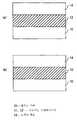
도 1은, 본 발명의 제1 실시의 형태에 따른 MISFET의 제조 방법과 그에 의해 얻어지는 반도체 장치를 설명하기 위한 단면도이다.1 is a cross-sectional view for explaining a method for manufacturing a MISFET and a semiconductor device obtained thereby according to the first embodiment of the present invention.
우선, 도 1의 (a)와 같이 실리콘 기판(10) 위에, 질소 첨가한 지르코늄 실리케이트막(12), 캡층(14)을 순서대로 적층한다. 또한, 질소 첨가한 지르코늄 실리케이트막(12)은 질소가 첨가된 지르코늄과 실리콘과의 화합물이며, 지르코늄과 실 리콘은 막 내의 깊이 방향으로 대략 균일한 조성 분포를 갖는다. 여기서, 지르코늄 실리케이트막(12)의 깊이 방향은, 캡층(14)과의 계면으로부터 실리콘 기판(10)과의 계면을 향하는 방향이다.First, as shown in FIG. 1A, the
캡층(14)은, 예를 들면 불순물을 첨가한 다결정 실리콘(폴리실리콘) 등의 도전성의 재료에 의해 형성한다.The
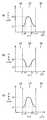
이 단계에서의 지르코늄 실리케이트막(12) 내의 각 원소의 깊이 방향의 조성 분포를 도 2의 각 도면을 이용하여 설명한다. 도 2의 (a)는 지르코늄의 농도 분포를 나타내고, 도 2의 (b)는 실리콘의 농도 분포를 나타내고, 도 2의 (c)는 질소의 농도 분포를 나타낸다. 지르코늄과 실리콘의 깊이 방향의 조성은, 똑같이 한다. 여기서는, 지르코늄의 원자 농도를 20at%, 실리콘의 원자 농도를 20at%로 하였다. 또한, 질소의 농도 분포는 캡층(14)측과 실리콘 기판(10)측에서 8at%로 낮게 하고, 중앙에서 40at%로 높게 한다. 이러한 조성 분포의 실현 방법은 후에 상세히 설명한다.Composition distribution in the depth direction of each element in the
다음으로, 이 적층막에 열 처리를 실시한다. 이 열 처리는, 예를 들면 질소 분위기 속에서 약 1000℃ 30초의 열 처리이다. 이 열 처리에 의해, 질소 농도가 낮은 층 영역에서 실리콘 원자와 금속 원자의 확산이 일어나, 지르코늄 실리케이트막(12)은 도 2의 (b)에 도시한 조성 분포가 변화한 지르코늄 실리케이트막(12')이 된다.Next, heat treatment is performed on this laminated film. This heat treatment is, for example, a heat treatment of about 1000 ° C. for 30 seconds in a nitrogen atmosphere. This heat treatment causes diffusion of silicon atoms and metal atoms in the layer region having a low nitrogen concentration, and the
이 지르코늄 실리케이트막(12') 내의 각 원소는, 도 3의 각 도면에 도시한 조성 분포를 갖는다. 즉, 실리콘은, 도 3의 (b)와 같이 실리콘 기판(10)측의 제1 층 영역, 및 캡층(14)측의 제2 층 영역으로 이동(편석)한다. 그 결과, 제1 층 영역이나 제2 층 영역에 비하여, 이들에 끼인 제3 층 영역의 실리콘이 감소한다(제1 및 제2 층 영역에서의 실리콘의 최대 농도는, 제3 층 영역에서의 실리콘의 농도의 각 최소값보다 높음).Each element in this zirconium silicate film 12 'has a composition distribution shown in each drawing of FIG. That is, silicon moves (segregates) to the 1st layer area | region on the
또한, 지르코늄 실리케이트막(12') 내의 지르코늄은, 도 3의 (a)와 같이 실리콘 기판(10) 측의 제1 층 영역과 캡층(14)측의 제2 층 영역에서 감소하고, 제3 층 영역을 향하여 이동한다. 이에 의해, 제3 층 영역에서의 지르코늄의 최대 농도는, 제1 및 제2 층 영역에서의 지르코늄의 농도의 각 최소값보다 높아진다.In addition, zirconium in the zirconium silicate film 12 'is reduced in the first layer region on the
또한, 제3 층 영역에 편석하고 있었던 질소는, 도 3의 (c)에 도시한 바와 같이 열 처리에 의해 제1 및 제2 층 영역으로 약간 이동하므로, 도 2의 (c)에 비하여 분포는 완만하게 된다(질소의 제3 층 영역에서의 최대 농도는, 제1 및 제2 층 영역에서의 농도의 최소값보다 높음).In addition, since nitrogen segregated in the third layer region moves slightly to the first and second layer regions by heat treatment as shown in Fig. 3C, the distribution is lower than that in Fig. 2C. It becomes gentle (the maximum concentration in the third layer region of nitrogen is higher than the minimum value of the concentration in the first and second layer regions).
즉, 본 실시의 형태의 지르코늄 실리케이트막은, 다음과 같은 질소 농도 분포를 갖는다. 조성 경사에 의해 의사 SiO2가 된 제1 및 제2 층 영역에서는 질소 농도가 상대적으로 낮고, 금속 농도가 높은 제3 층 영역에서는 질소 농도가 상대적으로 높은 구조이다.That is, the zirconium silicate film of this embodiment has the following nitrogen concentration distribution. The composition gradient by the doctor SiO2 has a first and a second layer region is relatively low nitrogen concentration, in the third layer region of high concentration of a metal structure, the nitrogen concentration is relatively high.
또한, 질소를 지르코늄 실리케이트막(12)에 첨가함으로써, 열 처리 공정에 있어서 금속 원자의 확산을 제어할 수 있다. 질소를 첨가한 지르코늄 실리케이트막(12)의 내부에서는 Si-N 결합이 형성되므로, 금속 원자(지르코늄)의 지르코늄 실 리케이트막 내에서의 확산을 억제할 수 있다. 이에 의해, 상분리 억제나 결정화 억제라는 효과를 기대할 수 있다.In addition, by adding nitrogen to the
또한, 지르코늄 실리케이트막(12)에의 질소 첨가에 의해, 캡층(14)으로부터 실리콘 기판(10)으로의 불순물 확산을 억제하는 효과도 기대할 수 있다. 즉, 캡층(14)으로서 붕소 등의 불순물을 첨가한 폴리실리콘을 이용한 경우에는, 붕소 등의 실리콘 기판(10)으로의 확산을 억제할 수 있다.In addition, the effect of suppressing the diffusion of impurities from the
또한, 지르코늄 실리케이트막(12)에 질소를 첨가함으로써, 최종적으로 형성되는 지르코늄 실리케이트막(12')의 내열성을 향상시켜, 그 결정화를 방지할 수 있다. 이 결정화의 억제에 의해 캡층(14)으로부터 실리콘 기판(10)에의 불순물의 「통과」를 더욱 억제할 수 있다.In addition, by adding nitrogen to the
또한, 지르코늄 실리케이트막(12') 내의 지르코늄 농도가 높을수록, 열 처리에 의해 결정화하기 쉬우므로, 지르코늄 농도가 높은 부분에서 질소 농도를 높게 함으로써, 층의 결정화를 억제할 수도 있다.In addition, the higher the zirconium concentration in the zirconium silicate film 12 ', the easier it is to crystallize by heat treatment. Therefore, the crystallization of the layer can be suppressed by increasing the nitrogen concentration in the high zirconium concentration.
이상, 상세하게 설명한 바와 같이 본 실시의 형태에 따르면, 용이하게 지르코늄 등의 금속 조성을 경사시킨 금속 실리케이트막을 형성할 수 있다.As described above, according to the present embodiment, the metal silicate film in which the metal composition such as zirconium is inclined can be easily formed.
또한, 본 실시의 형태에서는 금속 실리케이트막의 금속으로서 지르코늄을 예로 들어 설명하였다. 본 발명의 각 실시의 형태에 있어서, 지르코늄 대신에 하프늄, 티탄, 탄탈, 알루미늄, 이트륨, 란탄, 셀륨, 또는 그 밖의 희토류 원소를 이용할 수 있다.In the present embodiment, zirconium has been described as an example of the metal of the metal silicate film. In each embodiment of the present invention, hafnium, titanium, tantalum, aluminum, yttrium, lanthanum, selium or other rare earth elements can be used instead of zirconium.
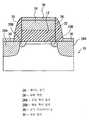
도 4는 MISFET를 설명하기 위한 게이트 길이 방향의 단면도이다.4 is a cross-sectional view in the gate length direction for explaining the MISFET.
즉, 실리콘 기판(10)의 주 표면 상에는, 상술한 경사 조성의 금속 실리케이트(12') 및 게이트 전극(24)을 적층한 MIS 구조가 형성되어 있다. 일반적으로, 금속 실리케이트막(12') 및 게이트 전극(24)은 도 5의 지면 수직 방향(게이트 폭 방향)으로 신장하는 단책(短冊) 형상을 갖는다.That is, on the main surface of the
게이트 전극(24)은 다결정 실리콘층으로 이루어진다. 게이트 전극(24)의 양 측벽에는 측벽 절연막(26)이 형성되어 있다. 게이트 전극(24)의 양편의 실리콘 기판(10) 표면에는, 고농도로 불순물이 확산된 한 쌍의 깊은 확산 영역(28A)과, 깊은 확산층(28A)과 게이트 전극(24) 사이에 형성된 얕은 확산 영역(28B)이 형성되어 있다. 또한, 깊은 확산 영역(28A)과 게이트 전극(24)의 다결정 실리콘층 상에는 금속 실리사이드층(30)이 형성되어 있다.The
또한, 한 쌍의 얕은 확산 영역(28B) 사이에는, 게이트에의 전압 인가에 의해 형성되는 채널 영역(32)이 형성되어 있다. 채널 영역은 트랜지스터의 임계값의 조정을 위해, 적절하게 첨가하는 불순물의 양이 조정되어 있다. 또한, 이 MISFET의 양편에는, 이웃의 소자와의 사이를 전기적으로 절연하는 소자 분리 영역이 일반적으로 형성된다(도시 생략).In addition, a
본 실시의 형태의 MISFET는 경사 조성을 갖는 금속 실리케이트막(12')이 게이트 절연막으로 작용하여, 높은 유전율로 높은 신뢰성이 얻어진다. 그 때문에, 게이트 전극(24)과 실리콘 기판(10)과의 사이의 누설 전류나 터널 전류를 억지할 수 있다.In the MISFET of this embodiment, the metal silicate film 12 'having an inclined composition acts as a gate insulating film, whereby high reliability at high dielectric constant is obtained. Therefore, leakage current and tunnel current between the
〈제2 실시의 형태〉<Second embodiment>
본 발명의 제2 실시의 형태에 따른 MISFET의 게이트 절연막의 제조 방법을 설명한다. 도 5의 (a), (b) 및 (c)는 제2 실시의 형태의 MISFET의 제조 방법을 설명하기 위한 공정 단면도이다.The manufacturing method of the gate insulating film of MISFET which concerns on 2nd Embodiment of this invention is demonstrated. 5 (a), 5 (b) and 5 (c) are cross-sectional views for illustrating the method for manufacturing the MISFET of the second embodiment.
우선, 소자 사이를 전기적으로 절연하는 소자 분리 영역(도시 생략)을 형성한 실리콘 기판(10)을 준비한다. 다음으로, 이 실리콘 기판(10)의 표면의 자연 산화막을 희불화수소산(HF) 용액 처리에 의해 제거하여, 실리콘 기판(10)의 표면의 미결합수(手)를 수소에 의해 종단하였다. 그리고, 균일 조성의 금속 실리케이트막(12)을 실리콘 기판(10)의 위에 형성하였다(도 5의 (a)). 금속 실리케이트막으로서, 예를 들면 두께 약 2㎚의 지르코늄 실리케이트막을 형성하였다. 이 때에는, 지르코늄 산화물 타깃과 실리콘 산화물 타깃을 이용하여, 아르곤과 산소, 질소의 혼합 가스 플라즈마를 이용한 스퍼터링을 이용하였다.First, a
이 때에는, 층의 깊이 방향에서 금속 및 실리콘이 균일한 조성이고, 또한 질소 농도의 깊이 방향의 중앙에서 높아지고, 실리콘 기판(10)과의 계면 부근 및 게이트 전극(14)과의 계면 부근에서 낮아지는 금속 실리케이트막(12)을 형성한다.At this time, the metal and silicon are uniform in the depth direction of the layer, and are increased in the center of the depth direction of the nitrogen concentration, and lower in the vicinity of the interface with the
형성 방법으로서는 스퍼터법 외에도, CVD법, 증착법 등을 이용할 수 있다.As the formation method, in addition to the sputtering method, a CVD method, a vapor deposition method, or the like can be used.
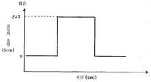
상술한 질소의 분포는, 예를 들면 스퍼터 내에 흐르는 질소(N2)의 유량을 시간에 따라 변화시킴으로써 실현할 수 있다. 도 6에 스퍼터 내의 질소(N2)의 유량의 시간에 따른 변화의 예를 모식적으로 나타낸다. 또한, 상기 질소 조성 분포는 질소를 함유하지 않는 금속 실리케이트막을 퇴적한 후, 조건(압력, 플라즈마의 종류)을 선택하여 행하는 플라즈마 질화에 의해, 실현할 수도 있다.The above-described distribution of nitrogen can be realized by, for example, changing the flow rate of nitrogen (N2 ) flowing in the sputtering with time. Figure 6 shows an example of a change with time of the flow rate of nitrogen (N2) in a sputtering schematically in. The nitrogen composition distribution can also be realized by plasma nitriding by selecting a condition (pressure, type of plasma) after depositing a metal silicate film containing no nitrogen.
이와 같이 하여 형성한 금속 실리케이트막(12)을 구비하는 실리콘 기판(10)을 열 처리함으로써, 제1 실시의 형태에서 설명한 바와 같은 경사 조성의 금속 실리케이트막(12')을 형성하였다.The
또한, 금속 실리케이트막의 조성 경사를 실현하는 다른 방법에는, 증착법이나 스퍼터법이 있다. 예를 들면, 증착 방법에서는 별개의 금속원과 실리콘원을 사용하여, 층의 형성 도중에 금속/실리콘비를 바꾸는 방법이 있다. 또한, 스퍼터에 있어서는 1종류의 조성의 타깃으로부터 경사 조성을 실현하는 것은 곤란하기 때문에, 조성이 다른 타깃을 사용하여, 층의 퇴적을 복수회로 나누어 행함으로써 경사 조성을 실현할 수 있다. 이들 방법은 막 내의 질소 농도가 높은 부분에서 금속 원자 및 실리콘 원자가 이동하기 어렵고, 질소 농도가 낮은 부분에서 금속 원자 및 실리콘 원자가 이동하기 쉽다는 현상에 기초하는 상술한 방법과 비교하면 약간 복잡한 제법이다. 여기서는 일례로서, 캡층(24)(게이트 전극)에 폴리실리콘을 이용하여, 승온 속도 100℃/초에서 승온한 후에, 1000℃의 질소 분위기 속에서 30초 동안의 열 처리를 행하였다. 이 열 처리에 의해, 조성 경사 금속 실리케이트막(12)을 형성할 수 있었다.In addition, another method of realizing the composition gradient of the metal silicate film includes a vapor deposition method and a sputtering method. For example, the deposition method uses a separate metal source and a silicon source to change the metal / silicon ratio during the formation of the layer. Moreover, in sputter | spatter, since it is difficult to implement | achieve an inclination composition from the target of one type of composition, inclination composition can be implement | achieved by dividing a layer into multiple times using the target from which a composition differs. These methods are slightly complicated in comparison with the above-mentioned method based on the phenomenon that metal atoms and silicon atoms are hard to move in the portion with high nitrogen concentration in the film, and metal atoms and silicon atoms are easily move in the portion with low nitrogen concentration. Here, as an example, polysilicon was used for the cap layer 24 (gate electrode), and the temperature was raised at a heating rate of 100 ° C / sec, followed by heat treatment for 30 seconds in a nitrogen atmosphere of 1000 ° C. By this heat treatment, the composition inclined
또한, 조성을 경사시키기 위한 고온 어닐링은 도 5의 (c)에 도시한 불순물 영역(10A, 10B)의 형성 공정에서 행하는 것이 아니라, 도 5의 (b)에 나타낸 게이트 전극 형성 후에 행할 수도 있다.In addition, the high temperature annealing for inclining the composition may be performed not after the formation of the
〈제3 실시의 형태〉<Third embodiment>
다음으로, 본 발명에 따른 제3 실시예에 대해서, 도 7 및 도 8을 이용하여 설명한다. 절연층에는, 금속 실리케이트뿐만 아니라, 실리콘을 적극적으로 첨가하지 않는 금속 산화물을 이용할 수도 있다. 제3 실시의 형태에서는, 이 금속 산화물에 의한 게이트 산화막에 대해서 설명한다.Next, a third embodiment according to the present invention will be described with reference to FIGS. 7 and 8. As the insulating layer, not only metal silicates, but also metal oxides without active addition of silicon can be used. In the third embodiment, the gate oxide film by the metal oxide will be described.
도 7은 실리콘 기판(10) 상에 금속 산화물막(34)을 형성하고, 또한 금속 산화물막(34) 상에 도전성 캡층(14)을 형성한 적층 구조의 단면도이다. 또한, 이 금속 산화물막(34) 내의 금속(예로서 Zr), 질소(N), 산소(O)의 농도 분포의 모식도를 도 8에 도시한다.FIG. 7 is a cross-sectional view of the laminated structure in which the
금속 산화물막(34) 내의 질소는, 실리콘 기판(10)과의 계면 부근(제1 층 영역), 및 도전성 캡층(14)과의 계면 부근(제2 층 영역)에서는 상대적으로 낮고, 그 사이(제3 층 영역)에서는 질소 농도가 상대적으로 높아지는 것과 같은 구조이다.Nitrogen in the
이러한 농도 분포에 의해, 금속 실리케이트막(12')과 마찬가지로, 제1 및 제2 층 영역에서, 제3 층 영역보다 밴드 갭을 크게 할 수 있으며, 누설 전류를 억제할 수 있다. 이 경우의 제조 방법은, 예를 들면 스퍼터 중에 도 8의 (b)에 도시한 바와 같이, 질소(N2)의 유량을 퇴적 시간에 따라 변화시킴으로써, 그 질소 조성 분포를 실현할 수 있다. 또한, 질소 조성 분포는 질소를 함유하지 않는 금속 산화물막을 퇴적한 후, 플라즈마 질화에 의해 실현할 수도 있다.By such a concentration distribution, the band gap can be made larger in the first and second layer regions than in the third layer region, as in the metal silicate film 12 ', and the leakage current can be suppressed. In this case, the nitrogen composition distribution can be realized by, for example, changing the flow rate of nitrogen (N2 ) in accordance with the deposition time, as shown in Fig. 8B in the sputter. The nitrogen composition distribution can also be realized by plasma nitriding after depositing a metal oxide film containing no nitrogen.
(제1 실시예)(First embodiment)
다음으로, 제1 실시의 형태에서 설명한 제조 방법의 구체예를 설명한다. 도 9의 (a), (b), (c), (d), (e) 및 (f)는, 질소 첨가한 지르코늄 실리케이트막의 열 처리 전후의, 막의 깊이 방향의 지르코늄과 실리콘의 조성 분포의 변화를 나타낸다.Next, the specific example of the manufacturing method demonstrated in 1st Embodiment is demonstrated. (A), (b), (c), (d), (e) and (f) of FIG. 9 show composition distributions of zirconium and silicon in the depth direction of the film before and after heat treatment of the nitrogen-added zirconium silicate film. Indicates a change.
도 9의 각 도면의 횡축은 지르코늄 실리케이트막(12, 12')의 캡층(14)과의 계면을 기점으로 하여 실리콘 기판(10)에 이르기까지의 깊이를 나타내고, 종축은 Zr나 Si의 농도(at%)를 나타낸다. 본 예에서의 지르코늄 실리케이트막(12)의 두께는 95Å이다.9, the horizontal axis represents the depth up to the
도 9의 (a)는 열 처리 전의 깊이 0Å으로부터 40Å까지의 분포를 나타내고, 도 9의 (b)는 그 열 처리 후의 분포를 나타낸다. 도 9의 (c)는 깊이 40Å으로부터 70Å까지의 열 처리 전의 분포를 나타내고, 도 9의 (d)는 그 열 처리 후의 분포를 나타내다. 또한, 도 9의 (e)는 깊이 75Å으로부터 95Å까지의 열 처리 전의 분포를 나타내고, 도 9의 (f)는 그 열 처리 후의 분포를 나타낸다. 이들 분포는 HR-RBS(High Resolution Ratheford Back Scattering)에 의해 측정하였다.FIG. 9 (a) shows a distribution from the depth of 0 kPa to 40 kPa before the heat treatment, and FIG. 9 (b) shows the distribution after the heat treatment. FIG. 9C shows a distribution before the heat treatment from the depth of 40 kPa to 70 kPa, and FIG. 9D shows the distribution after the heat treatment. 9E shows the distribution before the heat treatment from the depth of 75 kPa to 95 kPa, and FIG. 9 (f) shows the distribution after the heat treatment. These distributions were measured by HR-RBS (High Resolution Ratheford Back Scattering).
또한, 열 처리 전의 질소 농도는, 깊이 0Å으로부터 50Å까지를 8at%, 50Å으로부터 75Å까지를 40at%, 75Å으로부터 95Å까지를 8at%로 하고 있었다. 또한, 지르코늄과 실리콘의 농도는 층의 깊이 방향으로 대략 균일하게 하였다. 또한, 도 9의 (a)에서 Zr의 농도가 5at%까지 내려가 있지만, 원인으로서, C 등의 오염 물질이 표면측에 혼입하여, 상대적으로 Si, Zr 모두 원자 농도로서는 낮아지고 있기 때문이다. 그러나, 실제 반도체 장치 제조 공정과 같이 오염도가 적은 경우에는, 이러한 문제는 발생하지 않고, 또한 오염이 있어도 어닐링 후에는 오염 물질은 감소 한다. 도 9의 (a)의 단계에서, Zr은 완전히 균일한 것이 이상적이지만, 현실적으로는 변동하는 경우도 있다. 그 경우에는 변동량이 약 20% 이하이면, 원하는 효과가 얻어진다. 도 9의 (a)에 나타내는 Zr 농도도, 열 처리 후의 Zr의 농도 분포와 비교하여 보다 균일하다고 할 수 있다.In addition, the nitrogen concentration before heat processing made 8 at% of depth from 0 kPa to 50 kPa, 8 at% from 50 kPa to 75 kPa, and 40 at% and 75 kPa to 95 kPa. In addition, the concentrations of zirconium and silicon were made substantially uniform in the depth direction of the layer. In addition, although the concentration of Zr falls to 5at% in FIG.9 (a), as a cause, contaminants, such as C, mix in the surface side, and both Si and Zr are relatively low as atomic concentration. However, when the degree of contamination is small as in the actual semiconductor device manufacturing process, such a problem does not occur, and even if there is contamination, the pollutant is reduced after annealing. In the step (a) of FIG. 9, it is ideal that Zr is completely uniform, but it may fluctuate in reality. In that case, if the amount of variation is about 20% or less, the desired effect is obtained. It can be said that Zr concentration shown to Fig.9 (a) is also more uniform compared with the concentration distribution of Zr after heat processing.
도 9의 (b), (d) 및 (f)로부터 알 수 있듯이, 질소 농도가 낮은 실리콘 기판(10)측의 영역 및 도전성 캡층(14)측의 영역에서는, 열 처리에 의해 표면과 계면에서 Zr의 농도가 낮고, 내측에서 농도가 높은 분포를 실현할 수 있다.As can be seen from (b), (d) and (f) of FIG. 9, in the region on the
도 9의 (c) 및 (d)로부터, 열 처리 전에 질소 농도가 높아진 중앙 영역에서는 열 처리 후, 실리콘과 지르코늄은 거의 이동하지 않는 것을 알 수 있다. 이와 같이 제1 실시의 형태에 따른 제조 방법에 의해, 금속 조성이 경사진 금속 실리케이트막(12')을 형성할 수 있다.9C and 9D show that silicon and zirconium hardly move after the heat treatment in the central region where the nitrogen concentration is increased before the heat treatment. In this manner, the metal silicate film 12 'in which the metal composition is inclined can be formed by the manufacturing method according to the first embodiment.
이상, 실시의 형태나 실시예를 예시하면서 본 발명의 실시의 형태에 대하여 설명하였다. 그러나, 본 발명은 상술한 각 구체예로 한정되는 것이 아니며, 특허 청구의 범위에 기재된 요지에 따라, 적절하게 변경할 수 있다.As mentioned above, embodiment of this invention was described, demonstrating embodiment and an Example. However, the present invention is not limited to the specific examples described above, and may be appropriately changed in accordance with the gist of the claims.
예를 들면, 트랜지스터의 구조에 대해서도, 구체예로서 나타낸 것으로 한정되지 않고, 기타, 당업자가 본 발명을 적용하면서 설계 변경하여 얻을 수 있는 모든 트랜지스터는 본 발명의 범위에 포함된다.For example, also about the structure of a transistor, it is not limited to what was shown as a specific example, and all the transistors which can be obtained by design change while a person skilled in the art applies this invention are included in the scope of the present invention.
예를 들면, 트랜지스터의 각부를 구성하는 재료, 첨가 불순물, 막 두께, 형상, 도전형, 형성 방법 등에 대하여 당업자가 적절하게 설계 변경한 것은 본 발명의 범위에 포함된다.For example, design changes appropriately made by those skilled in the art to materials, additive impurities, film thicknesses, shapes, conductivity types, formation methods, and the like that constitute each part of the transistor are included in the scope of the present invention.
이상 상세하게 설명한 바와 같이, 본 발명에 따르면, 양호한 계면 특성을 유지하고, 또한 절연막의 누설 전류를 저감하는 금속 실리케이트막 등을 이용한 반도체 장치와 그 간편한 제조 방법을 제공할 수 있다.As described in detail above, according to the present invention, a semiconductor device using a metal silicate film or the like which maintains good interfacial characteristics and reduces leakage current of an insulating film can be provided, and a simple manufacturing method thereof.
Claims (6)
Translated fromKoreanApplications Claiming Priority (2)
| Application Number | Priority Date | Filing Date | Title |
|---|---|---|---|
| JPJP-P-2003-00048515 | 2003-02-26 | ||
| JP2003048515AJP4574951B2 (en) | 2003-02-26 | 2003-02-26 | Semiconductor device and manufacturing method thereof |
Publications (2)
| Publication Number | Publication Date |
|---|---|
| KR20040076798A KR20040076798A (en) | 2004-09-03 |
| KR100687153B1true KR100687153B1 (en) | 2007-02-27 |
Family
ID=32866603
Family Applications (1)
| Application Number | Title | Priority Date | Filing Date |
|---|---|---|---|
| KR1020040012553AExpired - Fee RelatedKR100687153B1 (en) | 2003-02-26 | 2004-02-25 | Semiconductor device and manufacturing method thereof |
Country Status (4)
| Country | Link |
|---|---|
| US (1) | US6849908B2 (en) |
| JP (1) | JP4574951B2 (en) |
| KR (1) | KR100687153B1 (en) |
| CN (2) | CN100356581C (en) |
Families Citing this family (18)
| Publication number | Priority date | Publication date | Assignee | Title |
|---|---|---|---|---|
| JP4120938B2 (en)* | 2001-08-23 | 2008-07-16 | 日本電気株式会社 | Semiconductor device having high dielectric constant insulating film and manufacturing method thereof |
| WO2004008544A1 (en) | 2002-07-16 | 2004-01-22 | Nec Corporation | Semiconductor device, production method and production device thereof |
| US6921702B2 (en)* | 2002-07-30 | 2005-07-26 | Micron Technology Inc. | Atomic layer deposited nanolaminates of HfO2/ZrO2 films as gate dielectrics |
| US7531467B2 (en) | 2004-01-21 | 2009-05-12 | Hitachi Kokusai Electric, Inc. | Manufacturing method of semiconductor device and substrate processing apparatus |
| JP2006013092A (en)* | 2004-06-25 | 2006-01-12 | Rohm Co Ltd | Semiconductor device and its fabrication process |
| US7081421B2 (en)* | 2004-08-26 | 2006-07-25 | Micron Technology, Inc. | Lanthanide oxide dielectric layer |
| US7588988B2 (en) | 2004-08-31 | 2009-09-15 | Micron Technology, Inc. | Method of forming apparatus having oxide films formed using atomic layer deposition |
| US7504700B2 (en)* | 2005-04-21 | 2009-03-17 | International Business Machines Corporation | Method of forming an ultra-thin [[HfSiO]] metal silicate film for high performance CMOS applications and semiconductor structure formed in said method |
| US7927948B2 (en) | 2005-07-20 | 2011-04-19 | Micron Technology, Inc. | Devices with nanocrystals and methods of formation |
| US8110469B2 (en)* | 2005-08-30 | 2012-02-07 | Micron Technology, Inc. | Graded dielectric layers |
| JP2007096151A (en)* | 2005-09-30 | 2007-04-12 | Toshiba Corp | Semiconductor memory device and manufacturing method thereof |
| US7812412B2 (en) | 2005-10-04 | 2010-10-12 | Nec Corporation | Semiconductor device |
| US8053849B2 (en)* | 2005-11-09 | 2011-11-08 | Advanced Micro Devices, Inc. | Replacement metal gate transistors with reduced gate oxide leakage |
| US8012822B2 (en)* | 2007-12-27 | 2011-09-06 | Canon Kabushiki Kaisha | Process for forming dielectric films |
| JP5442332B2 (en)* | 2009-06-26 | 2014-03-12 | ルネサスエレクトロニクス株式会社 | Semiconductor device and manufacturing method thereof |
| US9306024B2 (en)* | 2014-01-29 | 2016-04-05 | Taiwan Semiconductor Manufacturing Company Limited | Method of forming semiconductor device |
| JP6194516B2 (en) | 2014-08-29 | 2017-09-13 | 豊田合成株式会社 | MIS type semiconductor device |
| EP4026819A4 (en)* | 2019-09-02 | 2023-12-06 | Kabushiki Kaisha Toshiba | Joined body, circuit board, and semiconductor device |
Family Cites Families (9)
| Publication number | Priority date | Publication date | Assignee | Title |
|---|---|---|---|---|
| US4940233A (en)* | 1988-02-19 | 1990-07-10 | John Bull | Aerobic conditioning apparatus |
| JPH10242461A (en)* | 1997-02-27 | 1998-09-11 | Sony Corp | Semiconductor device and its manufacture |
| US6013553A (en)* | 1997-07-24 | 2000-01-11 | Texas Instruments Incorporated | Zirconium and/or hafnium oxynitride gate dielectric |
| JP2000049349A (en)* | 1998-07-15 | 2000-02-18 | Texas Instr Inc <Ti> | Method of manufacturing a field effect device on an integrated circuit |
| JP3833903B2 (en)* | 2000-07-11 | 2006-10-18 | 株式会社東芝 | Manufacturing method of semiconductor device |
| TW531803B (en)* | 2000-08-31 | 2003-05-11 | Agere Syst Guardian Corp | Electronic circuit structure with improved dielectric properties |
| US6500096B1 (en)* | 2000-11-29 | 2002-12-31 | Sinties Corporation, Inc. | Footbed for elliptical exercise machine |
| US6761665B2 (en)* | 2001-03-01 | 2004-07-13 | Hieu Trong Nguyen | Multi-function exercise apparatus |
| US7462134B2 (en)* | 2003-06-23 | 2008-12-09 | Nautilus, Inc. | Variable stride exercise device |
- 2003
- 2003-02-26JPJP2003048515Apatent/JP4574951B2/ennot_activeExpired - Fee Related
- 2004
- 2004-02-06USUS10/772,373patent/US6849908B2/ennot_activeExpired - Lifetime
- 2004-02-25KRKR1020040012553Apatent/KR100687153B1/ennot_activeExpired - Fee Related
- 2004-02-26CNCNB2004100684267Apatent/CN100356581C/ennot_activeExpired - Fee Related
- 2004-02-26CNCNB2007101120316Apatent/CN100485969C/ennot_activeExpired - Fee Related
Also Published As
| Publication number | Publication date |
|---|---|
| US20040164329A1 (en) | 2004-08-26 |
| CN100485969C (en) | 2009-05-06 |
| US6849908B2 (en) | 2005-02-01 |
| CN100356581C (en) | 2007-12-19 |
| KR20040076798A (en) | 2004-09-03 |
| JP4574951B2 (en) | 2010-11-04 |
| CN101075639A (en) | 2007-11-21 |
| JP2004259906A (en) | 2004-09-16 |
| CN1571166A (en) | 2005-01-26 |
Similar Documents
| Publication | Publication Date | Title |
|---|---|---|
| KR100687153B1 (en) | Semiconductor device and manufacturing method thereof | |
| US7655099B2 (en) | High-k dielectric film, method of forming the same and related semiconductor device | |
| US6914312B2 (en) | Field effect transistor having a MIS structure and method of fabricating the same | |
| US8168547B2 (en) | Manufacturing method of semiconductor device | |
| US6784101B1 (en) | Formation of high-k gate dielectric layers for MOS devices fabricated on strained lattice semiconductor substrates with minimized stress relaxation | |
| US7282773B2 (en) | Semiconductor device with high-k dielectric layer | |
| US7495264B2 (en) | Semiconductor device with high dielectric constant insulating film and manufacturing method for the same | |
| JP3688631B2 (en) | Manufacturing method of semiconductor device | |
| US6638877B2 (en) | Ultra-thin SiO2using N2O as the oxidant | |
| KR20050021311A (en) | Thin film formation method and semiconductor device manufacturing method | |
| JP2005317647A (en) | Semiconductor device and manufacturing method thereof | |
| JP2004335756A (en) | Semiconductor device and its manufacturing method | |
| US20030003667A1 (en) | Semiconductor device and method of fabricating the same | |
| JP2006344837A (en) | Semiconductor device and manufacturing method thereof | |
| US6777296B2 (en) | Semiconductor device and manufacturing method thereof | |
| JP5050351B2 (en) | Manufacturing method of semiconductor device | |
| US20050136580A1 (en) | Hydrogen free formation of gate electrodes | |
| JP3834564B2 (en) | Semiconductor device and manufacturing method thereof | |
| JP2005079563A (en) | Manufacturing method of electronic device | |
| JP4921887B2 (en) | Semiconductor device and manufacturing method thereof | |
| JP2006253267A (en) | Semiconductor device and its manufacturing method | |
| JP2006140514A (en) | Semiconductor device and manufacturing method thereof |
Legal Events
| Date | Code | Title | Description |
|---|---|---|---|
| A201 | Request for examination | ||
| PA0109 | Patent application | St.27 status event code:A-0-1-A10-A12-nap-PA0109 | |
| PA0201 | Request for examination | St.27 status event code:A-1-2-D10-D11-exm-PA0201 | |
| PG1501 | Laying open of application | St.27 status event code:A-1-1-Q10-Q12-nap-PG1501 | |
| E902 | Notification of reason for refusal | ||
| PE0902 | Notice of grounds for rejection | St.27 status event code:A-1-2-D10-D21-exm-PE0902 | |
| T11-X000 | Administrative time limit extension requested | St.27 status event code:U-3-3-T10-T11-oth-X000 | |
| T11-X000 | Administrative time limit extension requested | St.27 status event code:U-3-3-T10-T11-oth-X000 | |
| T11-X000 | Administrative time limit extension requested | St.27 status event code:U-3-3-T10-T11-oth-X000 | |
| T11-X000 | Administrative time limit extension requested | St.27 status event code:U-3-3-T10-T11-oth-X000 | |
| T11-X000 | Administrative time limit extension requested | St.27 status event code:U-3-3-T10-T11-oth-X000 | |
| T11-X000 | Administrative time limit extension requested | St.27 status event code:U-3-3-T10-T11-oth-X000 | |
| T11-X000 | Administrative time limit extension requested | St.27 status event code:U-3-3-T10-T11-oth-X000 | |
| T11-X000 | Administrative time limit extension requested | St.27 status event code:U-3-3-T10-T11-oth-X000 | |
| P11-X000 | Amendment of application requested | St.27 status event code:A-2-2-P10-P11-nap-X000 | |
| P13-X000 | Application amended | St.27 status event code:A-2-2-P10-P13-nap-X000 | |
| E701 | Decision to grant or registration of patent right | ||
| PE0701 | Decision of registration | St.27 status event code:A-1-2-D10-D22-exm-PE0701 | |
| GRNT | Written decision to grant | ||
| PR0701 | Registration of establishment | St.27 status event code:A-2-4-F10-F11-exm-PR0701 | |
| PR1002 | Payment of registration fee | St.27 status event code:A-2-2-U10-U11-oth-PR1002 Fee payment year number:1 | |
| PG1601 | Publication of registration | St.27 status event code:A-4-4-Q10-Q13-nap-PG1601 | |
| R17-X000 | Change to representative recorded | St.27 status event code:A-5-5-R10-R17-oth-X000 | |
| PR1001 | Payment of annual fee | St.27 status event code:A-4-4-U10-U11-oth-PR1001 Fee payment year number:4 | |
| PR1001 | Payment of annual fee | St.27 status event code:A-4-4-U10-U11-oth-PR1001 Fee payment year number:5 | |
| PR1001 | Payment of annual fee | St.27 status event code:A-4-4-U10-U11-oth-PR1001 Fee payment year number:6 | |
| FPAY | Annual fee payment | Payment date:20130201 Year of fee payment:7 | |
| PR1001 | Payment of annual fee | St.27 status event code:A-4-4-U10-U11-oth-PR1001 Fee payment year number:7 | |
| FPAY | Annual fee payment | Payment date:20140502 Year of fee payment:8 | |
| PR1001 | Payment of annual fee | St.27 status event code:A-4-4-U10-U11-oth-PR1001 Fee payment year number:8 | |
| FPAY | Annual fee payment | Payment date:20150120 Year of fee payment:9 | |
| PR1001 | Payment of annual fee | St.27 status event code:A-4-4-U10-U11-oth-PR1001 Fee payment year number:9 | |
| FPAY | Annual fee payment | Payment date:20160114 Year of fee payment:10 | |
| PR1001 | Payment of annual fee | St.27 status event code:A-4-4-U10-U11-oth-PR1001 Fee payment year number:10 | |
| FPAY | Annual fee payment | Payment date:20170119 Year of fee payment:11 | |
| PR1001 | Payment of annual fee | St.27 status event code:A-4-4-U10-U11-oth-PR1001 Fee payment year number:11 | |
| PN2301 | Change of applicant | St.27 status event code:A-5-5-R10-R11-asn-PN2301 | |
| PN2301 | Change of applicant | St.27 status event code:A-5-5-R10-R14-asn-PN2301 | |
| FPAY | Annual fee payment | Payment date:20180118 Year of fee payment:12 | |
| PR1001 | Payment of annual fee | St.27 status event code:A-4-4-U10-U11-oth-PR1001 Fee payment year number:12 | |
| FPAY | Annual fee payment | Payment date:20190116 Year of fee payment:13 | |
| PR1001 | Payment of annual fee | St.27 status event code:A-4-4-U10-U11-oth-PR1001 Fee payment year number:13 | |
| R18-X000 | Changes to party contact information recorded | St.27 status event code:A-5-5-R10-R18-oth-X000 | |
| FPAY | Annual fee payment | Payment date:20200205 Year of fee payment:14 | |
| PR1001 | Payment of annual fee | St.27 status event code:A-4-4-U10-U11-oth-PR1001 Fee payment year number:14 | |
| R18-X000 | Changes to party contact information recorded | St.27 status event code:A-5-5-R10-R18-oth-X000 | |
| PR1001 | Payment of annual fee | St.27 status event code:A-4-4-U10-U11-oth-PR1001 Fee payment year number:15 | |
| R18-X000 | Changes to party contact information recorded | St.27 status event code:A-5-5-R10-R18-oth-X000 | |
| R18-X000 | Changes to party contact information recorded | St.27 status event code:A-5-5-R10-R18-oth-X000 | |
| PC1903 | Unpaid annual fee | St.27 status event code:A-4-4-U10-U13-oth-PC1903 Not in force date:20220221 Payment event data comment text:Termination Category : DEFAULT_OF_REGISTRATION_FEE | |
| PC1903 | Unpaid annual fee | St.27 status event code:N-4-6-H10-H13-oth-PC1903 Ip right cessation event data comment text:Termination Category : DEFAULT_OF_REGISTRATION_FEE Not in force date:20220221 | |
| P22-X000 | Classification modified | St.27 status event code:A-4-4-P10-P22-nap-X000 | |
| R18-X000 | Changes to party contact information recorded | St.27 status event code:A-5-5-R10-R18-oth-X000 |