KR100685954B1 - Touch panel - Google Patents
Touch panelDownload PDFInfo
- Publication number
- KR100685954B1 KR100685954B1KR1020020083300AKR20020083300AKR100685954B1KR 100685954 B1KR100685954 B1KR 100685954B1KR 1020020083300 AKR1020020083300 AKR 1020020083300AKR 20020083300 AKR20020083300 AKR 20020083300AKR 100685954 B1KR100685954 B1KR 100685954B1
- Authority
- KR
- South Korea
- Prior art keywords
- transparent conductive
- touch panel
- conductive film
- film
- pen
- Prior art date
- Legal status (The legal status is an assumption and is not a legal conclusion. Google has not performed a legal analysis and makes no representation as to the accuracy of the status listed.)
- Expired - Lifetime
Links
Images


Classifications
- G—PHYSICS
- G06—COMPUTING OR CALCULATING; COUNTING
- G06F—ELECTRIC DIGITAL DATA PROCESSING
- G06F3/00—Input arrangements for transferring data to be processed into a form capable of being handled by the computer; Output arrangements for transferring data from processing unit to output unit, e.g. interface arrangements
- G06F3/01—Input arrangements or combined input and output arrangements for interaction between user and computer
- G06F3/03—Arrangements for converting the position or the displacement of a member into a coded form
- G06F3/041—Digitisers, e.g. for touch screens or touch pads, characterised by the transducing means
- G06F3/044—Digitisers, e.g. for touch screens or touch pads, characterised by the transducing means by capacitive means
- G06F3/0445—Digitisers, e.g. for touch screens or touch pads, characterised by the transducing means by capacitive means using two or more layers of sensing electrodes, e.g. using two layers of electrodes separated by a dielectric layer
- G—PHYSICS
- G06—COMPUTING OR CALCULATING; COUNTING
- G06F—ELECTRIC DIGITAL DATA PROCESSING
- G06F3/00—Input arrangements for transferring data to be processed into a form capable of being handled by the computer; Output arrangements for transferring data from processing unit to output unit, e.g. interface arrangements
- G06F3/01—Input arrangements or combined input and output arrangements for interaction between user and computer
- G06F3/03—Arrangements for converting the position or the displacement of a member into a coded form
- G06F3/041—Digitisers, e.g. for touch screens or touch pads, characterised by the transducing means
- G06F3/044—Digitisers, e.g. for touch screens or touch pads, characterised by the transducing means by capacitive means
- G06F3/0444—Digitisers, e.g. for touch screens or touch pads, characterised by the transducing means by capacitive means using a single conductive element covering the whole sensing surface, e.g. by sensing the electrical current flowing at the corners
- G—PHYSICS
- G06—COMPUTING OR CALCULATING; COUNTING
- G06F—ELECTRIC DIGITAL DATA PROCESSING
- G06F3/00—Input arrangements for transferring data to be processed into a form capable of being handled by the computer; Output arrangements for transferring data from processing unit to output unit, e.g. interface arrangements
- G06F3/01—Input arrangements or combined input and output arrangements for interaction between user and computer
- G06F3/03—Arrangements for converting the position or the displacement of a member into a coded form
- G—PHYSICS
- G06—COMPUTING OR CALCULATING; COUNTING
- G06F—ELECTRIC DIGITAL DATA PROCESSING
- G06F2203/00—Indexing scheme relating to G06F3/00 - G06F3/048
- G06F2203/041—Indexing scheme relating to G06F3/041 - G06F3/045
- G06F2203/04103—Manufacturing, i.e. details related to manufacturing processes specially suited for touch sensitive devices
Landscapes
- Engineering & Computer Science (AREA)
- General Engineering & Computer Science (AREA)
- Theoretical Computer Science (AREA)
- Human Computer Interaction (AREA)
- Physics & Mathematics (AREA)
- General Physics & Mathematics (AREA)
- Position Input By Displaying (AREA)
Abstract
Translated fromKoreanDescription
Translated fromKorean도 1은 일반적인 정전 용량 방식의 터치 패널 및 그 동작 원리를 나타낸 개략적인 도면1 is a schematic diagram showing a general capacitive touch panel and its operation principle
도 2는 일반적인 정전 용량 방식의 터치 패널을 나타낸 평면도2 is a plan view showing a typical capacitive touch panel
도 3은 도 2의 I~I' 선상의 구조 단면도3 is a cross-sectional view taken along line II ′ of FIG. 2;
도 4는 정전 용량 방식의 터치 패널의 구동 원리를 나타낸 블록도4 is a block diagram illustrating a driving principle of a capacitive touch panel.
도 5a 및 도 5b는 본 발명의 터치 패널의 하부 필름 및 상부 필름을 나타낸 평면도5A and 5B are plan views illustrating a lower film and an upper film of the touch panel of the present invention.
도 6은 도 5a 및 도 5b의 하부 필름 및 상부 필름이 합착된 모습을 나타낸 평면도FIG. 6 is a plan view illustrating a state in which the lower film and the upper film of FIGS. 5A and 5B are bonded together.
도 7은 도 5a, 도 5b 및 도 6의 Ⅱ~Ⅱ' 선상의 구조 단면도7 is a structural cross-sectional view taken along line II-II 'of FIGS. 5A, 5B, and 6.
도 8은 도 6의 Ⅲ~Ⅲ' 선상의 구조 단면도FIG. 8 is a cross-sectional view taken along line III-III 'of FIG. 6
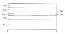
*도면의 주요 부분에 대한 부호 설명** Description of symbols on the main parts of the drawings *
105 : 유리 기판 107 : 제 1 투명 도전막105: glass substrate 107: first transparent conductive film
110a, 110b, 110c, 110d, 210 : 금속 전극 120 : 도트 스페이서110a, 110b, 110c, 110d, 210: metal electrode 120: dot spacer
203 : PET 필름 205 : 제 2 투명 도전막203: PET film 205: second transparent conductive film
220 : 절연성 접착제220: insulating adhesive
본 발명은 표시 장치를 일체형으로 형성하는 터치 패널에 관한 것으로 특히, 정전 용량 방식에 저항막 방식을 결합하여 전도성 펜뿐만 아니라 장갑 낀 손이나 비도전성 펜 등에까지 입력 도구의 재질을 확장시킨 터치 패널에 관한 것이다.The present invention relates to a touch panel in which a display device is integrally formed, and more particularly, to a touch panel in which a material of an input tool is extended not only to a conductive pen but also to a gloved hand or a non-conductive pen by combining a resistive method with a capacitive type. It is about.
개인용 컴퓨터, 휴대용 전송 장치 그 밖의 개인전용 정보 처리 장치 등은 키보드, 마우스, 디지타이저(Digitizer) 등의 다양한 입력 장치(Input Device)를 이용하여 텍스트 및 그래픽 처리 등을 수행한다.A personal computer, a portable transmission device, and other personal information processing devices perform text and graphics processing using various input devices such as a keyboard, a mouse, and a digitizer.
이러한 입력 장치들은 PC의 용도 확대에 따라 인터페이스로서의 입력 장치로서 키보드 및 마우스만으로는 제품 대응이 어렵고 보다 간단하고 오조작은 적으면서 누구라도 입력할 수 있고 또 휴대하면서 손으로 문자입력도 가능한 필요성에 의해 발전했다.These input devices have been developed due to the necessity of being able to input anybody with simple keyboard, mouse, and small input, and to input text by hand while being used as a keyboard as a interface device as an interface device. .
현재는 이러한 입력 장치의 일반적 기능과 관련된 필요성을 충족시키는 수준을 넘어 고신뢰성, 새로운 기능의 제공, 내구성, 재료나 물질을 포함한 설계 및 가공과 관련된 제조 기술 등과 같이 미세한 기술로 관심이 바뀌고 있다.Nowadays, attention is shifting to more sophisticated technologies such as high reliability, the provision of new features, durability, and manufacturing techniques related to design and processing involving materials or materials, beyond meeting the needs associated with the general functions of these input devices.
특히, 간단하고, 오조작이 적으며, 휴대하면서 누구라도 입력이 가능하고, 다른 입력기기 없이 문자 입력도 가능한 입력 장치로서 터치 패널(Touch Panel)이 알려져 있으며, 그에 따른 검출 방식, 구조 및 성능 등에 있어서도 자세히 알려져 있다.In particular, a touch panel is known as an input device that is simple, has low misoperation, can be input by anyone while carrying it, and can input characters without other input devices. Also known in detail.
검출 방식에 따라 간단히 살펴보면, 상판 또는 하판에 금속 전극을 형성하여 직류 전압을 인가한 상태에서 눌려진 위치를 저항에 따른 전압 구배로 판단하는 저항막 방식(Resistive type)과, 도전막에 등전위를 형성하여 상하판의 접촉시 전압 변화가 일어난 위치를 감지하는 정전 용량 방식(Capacitive type)과, 전자펜으로 도전막을 접촉하여 유도된 LC 값을 읽어들어 위치를 감지하는 전자 유도 방식(Electro Magnetic type) 등이 있다.In brief, according to the detection method, a metal electrode is formed on the upper plate or the lower plate and a resistive type that determines the pressed position in the state where the DC voltage is applied is regarded as a voltage gradient according to the resistance, and an equipotential is formed on the conductive film. Capacitive type to detect the position where the voltage change occurs when the upper and lower plates are contacted, and Electro Magnetic type to detect the position by reading the LC value induced by contacting the conductive film with the electronic pen, etc. have.
각각의 방식에 따라 신호 증폭의 문제나 해상도 차이, 설계 및 가공 기술의 난이도 차이 등이 다르게 나타나는 특징이 있어 장점을 잘 살릴 수 있게 구분하여 그 방식을 선택한다. 선택 기준은 광학적 특성, 전기적 특성, 기계적 특성, 내환경 특성, 입력 특성 외에 내구성과 경제성 등도 고려된다.Each method has different characteristics such as signal amplification problem, resolution difference, and difficulty in design and processing technology. Selection criteria include optical, electrical, mechanical, environmental and input characteristics, as well as durability and economy.
이하, 첨부된 도면을 참조하여 종래의 터치 패널을 설명하면 다음과 같다.Hereinafter, a conventional touch panel will be described with reference to the accompanying drawings.
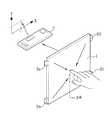
도 1은 일반적인 정전 용량 방식의 터치 패널 및 그 동작 원리를 나타낸 개략적인 도면이다.1 is a schematic diagram illustrating a general capacitive touch panel and an operating principle thereof.
도 1과 같이, 일반적인 정전 용량 방식의 터치 패널은 투명 도전막(1)으로 코팅된 곡면 또는 평면 유리 기판(도 2의 10참조)의 각 모서리에 등전위가 생성되도록 금속 전극들(2a, 2b, 2c, 2d)을 위치시켜 구성된다.As shown in FIG. 1, a typical capacitive touch panel includes
상기 금속 전극들(2a, 2b, 2c, 2d)을 통해 상기 투명 도전막(1)은 전압을 인가받아 전면에 등전위를 이루고 있으며, 터치 패널의 터치 동작이 일어났을 때, 전압 강하(Voltage drop)가 나타난다.The transparent conductive layer 1 is equipotentially applied to the front surface by applying a voltage through the
이러한 전압 강하치를 컨트롤러를 통해 감지하여 터치가 일어난 위치를 찾는 것이 정전 용량 방식의 동작 원리이다.Capacitive type operation principle is to detect the voltage drop through the controller to find the location where the touch occurred.
상기 정전 용량 방식의 터치 패널의 입력 도구로는 맨 손(Bare finger) 또는 전도성 스타일러스 펜(Conductive Stylus Pen)으로서, 도전성이 있는 재료로서 터치 패널의 입력면에 접촉이 일어났을 때, 접촉 부위의 전압 강하를 유발할 수 있는 성분이어야 한다.An input tool of the capacitive touch panel is a bare finger or a conductive stylus pen, which is a conductive material, and when a contact occurs on an input surface of the touch panel, a voltage of a contact portion It should be an ingredient that can cause a drop.
이하, 터치 패널의 평면도 및 단면도를 통해 종래의 정전 용량 방식의 터치 패널에 대해 살펴본다.Hereinafter, a conventional capacitive touch panel will be described with reference to a plan view and a cross-sectional view of the touch panel.
도 2는 종래의 정전 용량 방식의 터치 패널에 관한 평면도이며, 도 3은 도 2의 I~I' 선상의 구조 단면도이다.2 is a plan view of a conventional capacitive touch panel, and FIG. 3 is a cross-sectional view taken along line II ′ of FIG. 2.
도 2 및 도 3과 같이, 종래의 정전 용량 방식의 터치 패널은 지지기판이 유리 기판 상에 투명 도전막이 형성되며, 상기 투명 도전막의 네 모서리 각각에 전압 인가용 금속 전극이 형성되어 있다.2 and 3, in a conventional capacitive touch panel, a support substrate is formed of a transparent conductive film on a glass substrate, and metal electrodes for voltage application are formed at each of four corners of the transparent conductive film.
상기 투명 도전막(1)은 ITO(Indium Tin Oxide) 또는 ATO(Antimony Tin Oxide) 등의 투명한 금속으로 형성되며, 상기 투명 도전막(1)의 지지기판인 유리 기판(10)은 통상의 소다라임 글래스(Soda-lime glass)로 형성한다.The transparent conductive film 1 is formed of a transparent metal such as indium tin oxide (ITO) or antimony tin oxide (ATO), and the
그리고, 상기 투명 도전막(1)의 네 모서리에 형성되는 금속 전극들(2a, 2b, 2c, 2d)은 은(Ag) 등의 저항률이 낮은 도전성 금속으로 프린팅하여 형성한다.The
상기 금속 전극들(2a, 2b, 2c, 2d)의 주변에는 저항 네트워크가 형성된다. 상기 저항 네트워크는 상기 투명 도전막(1)의 표면 전체에 균등하게 컨트롤 신호를 송출하기 위하여 선형성 패턴(Linearization Pattern)으로 형성된다.A resistance network is formed around the
도시되지 않았지만, 상기 금속 전극들(2a, 2b, 2c, 2d)을 포함한 투명 도전막(1)의 상부에는 보호막이 코팅된다. 재질은 액체 글래스지만 열처리한 후, 경화/고밀도화 과정을 거쳐 하트 코팅재로 기능하게 한다.Although not shown, a protective film is coated on the transparent conductive film 1 including the
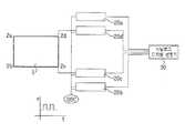
도 4는 일반적인 정전 용량 방식의 터치 패널의 구동 원리를 나타낸 블록도이다.4 is a block diagram illustrating a driving principle of a general capacitive touch panel.
도 4와 같이, 정전 용량 방식의 터치 패널은 투명 도전막(1)의 4 모서리의 위치한 각각의 금속 전극(2a, 2b, 2c, 2d)에 전압을 걸어주면 구석에서 발생되는 고주파가 터치 패널 전면에 퍼지게 된다. 이 때, 손가락 또는 전도성 펜으로 상기 투명 도전막(1)을 접촉하게 되면 각각의 전류 센서(20a, 20b, 20c, 20d)에서는 전류의 변화를 감지한다.As shown in FIG. 4, in the capacitive touch panel, when a voltage is applied to each of the
상기 전류 센서(20a, 20b, 20c, 20d) 및 아날로그-디지털 변환기(30)는 컨트롤러(도 1의 3 참조)에 구성되는 블록이다.The
상기 컨트롤러(3)는 내부의 오실레이터(OSC)를 통해 수십 킬로 Hz의 방형파를 전류 센서(20a, 20b, 20c, 20d)로 공급하여, 상기 전류 센서(20a, 20b, 20c, 20d)의 충전과 방전을 지속적으로 행하며, 아날로그-디지털 변환기(30)를 통해 적분 기간(통상 8msec)동안 충전량을 디지털적으로 적분한다. 이를 통해 접촉 여부를 판단하고, 좌표치를 계산하여 시스템(미도시)에 정보로 출력한다.The controller 3 supplies a square wave of several tens of kilo Hz to the
이와 같이, 정전 용량 방식은 입력 도구로서 컨트롤러(3)로부터 신호를 인가받는 전도성 펜 또는 손가락(bare finger)만이 적용되었다. 따라서, 전도성 펜을 분실하거나 실험 도중 장갑 낀 손으로 터치 패널을 접촉시에는 위치 감지 능력이 떨어졌다.As such, in the capacitive type, only a conductive pen or a bare finger that receives a signal from the controller 3 is applied as an input tool. Therefore, the position sensing ability was lost when the conductive pen was lost or when the touch panel was touched with gloved hands during the experiment.
한편, 저항막 방식의 터치 패널은 상부 전극이 형성되어 있는 상부 기판에 펜 또는 손가락 같은 소정의 입력 수단으로 어느 한 지점에 접촉하게 되면, 상부 기판에 형성된 상부 전극과 하부 기판에 형성된 하부 전극이 상호 통전되고, 그 위치의 저항 값에 의하여 변화된 전압 값을 읽어들인 후 제어부에서 전위차의 변화에 따라 위치 좌표를 찾게되는 장치이다.On the other hand, in the resistive touch panel, when a contact point is contacted with a predetermined input means such as a pen or a finger on the upper substrate on which the upper electrode is formed, the upper electrode formed on the upper substrate and the lower electrode formed on the lower substrate mutually It is a device that is energized and reads the voltage value changed by the resistance value of the position, and then finds the position coordinate according to the change of the potential difference in the controller.
이러한 저항막 방식은 입력 도구의 관계없이, 접촉을 행하는 위치에 대하여 인식이 가능하므로, 전도성 펜이 특별히 요구되지 않아, 실험 중에 장갑 낀 손이나, 비전도성 펜으로도 충분히 위치 검출이 가능하였다.Since the resistive film system can recognize the contact position regardless of the input tool, a conductive pen is not particularly required, and the position can be sufficiently detected by a gloved hand or a non-conductive pen during the experiment.
그러나, 정전 용량 방식과 달리 투명 도전막에 분포되는 저항의 의해 위치가 정해지므로, 부정확한 위치 검출이 이루어질 수 있어 정전 용량 방식에 비해 정확성이나 해상도면에서는 효율이 떨어지는 문제점이 있다.However, unlike the capacitive method, since the position is determined by the resistance distributed in the transparent conductive film, inaccurate position detection can be made, which leads to a problem in that the efficiency and the resolution are inferior to the capacitive method.
상기와 같은 종래의 터치 패널은 다음과 같은 문제점이 있다.The conventional touch panel as described above has the following problems.
정전 용량 방식은 비전도성 입력 도구, 예를 들어, 장갑 낀 손이나 비전도성 펜으로는 터치 패널의 입력면에 터치 동작이 이루어지더라도 위치 검출이 되지 안았다.In the capacitive type, a non-conductive input tool such as a gloved hand or a non-conductive pen does not detect a position even when a touch operation is made on the input surface of the touch panel.
따라서, 전도성 펜을 분실하거나, 또는 실험 중에 장갑 낀 손을 입력 도구로 사용할 경우, 상기 터치 패널은 입력 장치로서 기능을 못하게 된다.Therefore, if the conductive pen is lost or if a gloved hand is used as an input tool during the experiment, the touch panel will not function as an input device.
이와 같이, 외부 조건에 따라 제약을 받는 정전 용량 방식에 장갑 낀 손이나 부도체 등의 입력 도구로도 사용 가능한 저항막 방식을 적용시켜 터치 패널의 입력 도구의 사용예를 늘리고, 환경이 변하더라도 사용 가능한 터치 패널의 요구가 필요하였다.In this way, the resistive method, which can be used as an input tool such as a gloved hand or a non-conductor, is applied to the capacitive method, which is restricted by external conditions, to increase the use example of the touch panel input tool and to use it even if the environment changes. There was a need for a touch panel.
본 발명은 상기와 같은 문제점을 해결하기 위해 안출한 것으로, 정전 용량 방식에 저항막 방식을 결합하여 전도성 펜뿐만 아니라 장갑 낀 손이나 비도전성 펜 등에까지 입력 도구의 재질을 확장시킨 터치 패널을 제공하는 데, 그 목적이 있다.The present invention has been made to solve the above problems, by combining a resistive method with a capacitive method to provide a touch panel that extends the material of the input tool to not only a conductive pen but also a gloved hand or a non-conductive pen. There is a purpose.
상기와 같은 목적을 달성하기 위한 본 발명의 터치 패널은 지지필름과, 상기 지지필름 상에 전압인가를 위한 금속 전극을 구비하여 형성된 제 1 투명 도전막과, 상기 제 1 투명 도전막과 마주보며 일측에 신호 검출 전극을 구비한 제 2 투명 도전막과, 상기 제 1, 제 2 투명 도전막을 서로 부착하도록 가장 자리에 형성된 양면 접착제와, 상기 제 2 투명 도전막 상에 보호용 필름을 포함하여 이루어짐에 그 특징이 있다.The touch panel of the present invention for achieving the above object has a support film, a first transparent conductive film formed with a metal electrode for applying voltage on the support film, and one side facing the first transparent conductive film A second transparent conductive film having a signal detection electrode on the substrate, a double-sided adhesive formed at an edge to attach the first and second transparent conductive films to each other, and a protective film on the second transparent conductive film. There is a characteristic.
상기 지지필름은 하부에 차폐용 투명 도전막을 더 구비함이 바람직하다.The support film is preferably further provided with a shielding transparent conductive film at the bottom.
상기 양면 접착제는 절연성 물질로 이루어진 것임이 바람직하다.The double-sided adhesive is preferably made of an insulating material.
상기 금속 전극은 제 1 투명 도전막의 4 모서리에 각각 형성된 것이 바람직하다.Preferably, the metal electrodes are formed at four corners of the first transparent conductive film.
상기 신호 검출 전극은 제 2 투명 도전막의 가장 자리 일측에 형성된 것이 바람직하다.The signal detection electrode is preferably formed on one side of the edge of the second transparent conductive film.
상기 보호용 필름은 유리 기판 또는 투명 필름으로 이루어진 것이 바람직하 다.The protective film is preferably made of a glass substrate or a transparent film.
이하, 첨부된 도면을 참조하여 본 발명의 터치 패널을 상세히 설명하면 다음과 같다.Hereinafter, the touch panel of the present invention will be described in detail with reference to the accompanying drawings.
도 5a 및 도 5b는 본 발명의 터치 패널의 하부 필름 및 상부 필름을 나타낸 평면도이며, 도 6은 도 5a 및 도 5b의 하부 필름 및 상부 필름이 합착된 모습을 나타낸 평면도이며, 도 7은 도 5a, 도 5b 및 도 6의 Ⅱ~Ⅱ' 선상의 구조 단면도, 도 8은 도 6의 Ⅲ~Ⅲ' 선상의 구조 단면도이다.5A and 5B are plan views illustrating the lower film and the upper film of the touch panel of the present invention, and FIG. 6 is a plan view showing the lower film and the upper film of FIGS. 5A and 5B bonded together, and FIG. 7 is FIG. 5A. , FIG. 5B and FIG. 6 are cross-sectional views taken along the line II-II ', and FIG. 8 is a cross-sectional view taken along the line III-III' of FIG. 6.
본 발명의 터치 패널은 유리 기판(도 7의 105 참조)을 지지기판으로 하여 도 5a와 같이, 제 1 투명 도전막(107)을 형성한 후, 상기 제 1 투명 도전막(107)의 네 모서리에 각각 금속 전극(110a, 110b, 110c, 110d)을 형성한다. 또한, 제 1 투명 도전막(107) 상에는 하부에 형성되는 표시부에 대응하는 영역에 도트 스페이서(120)를 소정 간격 이격하여 복수개 형성한다.In the touch panel of the present invention, as shown in FIG. 5A, using a glass substrate (see 105 in FIG. 7) as a support substrate, four corners of the first transparent
그리고, 상기 제 1 투명 도전막(107)과 대응하여 도 5b와 같이, 제 2 투명 도전막(205) 상의 일측에 금속 전극(210)을 형성한다.5B, the
도 6과 같이, 상기 제 1 투명 도전막(107)의 금속 전극들과 상기 제 2 투명 도전막(205)의 금속 전극(210)을 마주보도록 하여 두 도전막(107, 205) 사이에 절연성 접착제(220)를 개재하여 부착한다. 이 때, 상기 절연성 접착제(220)는 상기 제 1, 제 2 투명 도전막(107, 205)의 주변부(데드 스페이스)에 대응하도록 형성한다.As shown in FIG. 6, an insulating adhesive is formed between the two
도시되어 있는 바에 따르면, 상기 제 1 투명 도전막(107) 상의 금속 전극과 상기 제 2 투명 도전막(205) 상의 금속 전극(210)과 오버랩되어 형성되어 있지만, 상기 금속 전극이 가지는 높이로 인해 터치 패널면에서 가지는 단차를 줄이기 위해 제 2 투명 도전막(205)의 금속 전극(210)을 모서리가 아닌 데드 스페이스(dead space)의 가운데 부분이나, 그 외 소정 영역으로 이동하여 형성할 수 있다.As illustrated, although the metal electrode on the first transparent
도 7 및 도 8과 같이, 본 발명의 터치 패널의 단면도에 따르면 상기 각 금속 전극(110a, 110b, 110c, 110d, 210)이 형성되어 있는 부위는 터치 패널의 데드 스페이스이고, 데드 스페이스에 해당되는 부위는 제 1, 제 2 투명 도전막(107, 205)의 접착 부위로서, 상기 금속 전극들(110a, 110b, 110c, 110d, 210)을 포함하여 절연성 접착제(220)가 형성되어, 상기 제 1, 제 2 투명 도전막(107, 205) 상의 금속 전극들(110a, 110b, 110c, 110d, 210)이 서로 접촉하지 않도록 한다.7 and 8, according to the cross-sectional view of the touch panel of the present invention, a portion where each of the
상기 제 1 투명 도전막(107)은 유리 기판(105) 상에 형성되며, 네 모서리에 금속 전극(110a, 110b, 110c, 110d)이 형성되어, 외부로부터 등전위 형성용 전압 신호를 인가받는다.The first transparent
상기 유리 기판(105)은 지지기판으로서, 터치 패널면에 손가락 또는 펜 등에 의해 접촉 또는 드로잉(drawing) 동작이 여러 번 이루어져도, 그 충격에 의해 상기 제 1, 제 2 투명 도전막(107)이 깨짐을 방지하는 역할을 한다. 상기 지지기판으로서의 역할을 필름 타입의 기판으로서도 그 기능을 기대할 수 있다.The
도시되어 있지 않지만, 상기 유리 기판(105)의 하부에는 제 1 투명 도전막(107)과 대칭적으로 투명 도전막을 더 형성하고 이를 접지함으로써, 터치 패널 하부에 형성되는 표시 장치에서의 노이즈가 상기 터치 패널측으로 유입되는 것 을 방지할 수 있다.Although not shown, the transparent conductive film is further formed below the
또한, 상기 제 2 투명 도전막(205) 상부의 PET(Poly Ethylene Terephtalate) 필름(203)은 보호막으로 기능하며, 또한, 투명한 플라스틱 물질로서 내구성 및 필기감을 향상시킬 수 있다.In addition, the PET (Poly Ethylene Terephtalate)
그리고, 상기 제 1 투명 도전막(107)과 마주 보는 상기 제 2 투명 도전막(205)의 내측면에 형성된 금속 전극(210)은 외부의 접지 전원 또는 금속 쉴드 성분과 만나 터치 패널면의 접촉이 일어났을 때, 상기 제 2 투명 도전막(205)을 접지시키는 역할을 한다.In addition, the
따라서, 손가락 또는 전도성 펜 등이 입력 도구로 사용되었을 때는 접촉 동작 후, 접촉 부위를 기점으로 상기 제 1 투명 도전막(107)의 형성된 등전위가 파괴되어, 전류가 발생하고, 전류가 흐름에 따라 충전된 전하량을 상기 제 1 투명 도전막(107) 상에 형성된 금속 전극들(110a, 110b, 110c, 110d)에 연결된 전류 센서를 통해 감지하고, 아날로그-디지털 변환기를 통해 변환하여 위치를 검출하고, 상기 손가락 또는 전도성 펜 등을 방전 수단으로 이용하며, 장갑 낀 손가락이나 비전도성 펜 등이 입력 도구로 사용되었을 때는 같은 방식으로 충전된 전하량으로 위치를 검출한 후, 상기 제 2 투명 도전막(205)을 상기 금속 전극(210)을 통해 접지시켜 방전시킨다.Therefore, when a finger or a conductive pen or the like is used as an input tool, after the contacting operation, the formed equipotential of the first transparent
도 8과 같이, 본 발명의 터치 패널은 마주보는 제 1, 제 2 투명 도전막(107, 205)의 주변부에 형성되는 절연성 접착제(220)를 제외한 터치 패널의 표시 영역에 도트 스페이서(120)가 형성되어 상기 제 1, 제 2 투명 도전막(107, 205) 사이의 소 정 갭을 유지하도록 한다.As illustrated in FIG. 8, in the touch panel of the present invention, the
또한, 상기 제 2 투명 도전막(205) 상부의 PET(Poly Ethylene Terephtalate) 필름(203)은 종래의 정전 용량 방식에서 직접적으로 도전성 물질이 닿는 것을 방지하고, 보호막으로 기능하며, 또한, 플라스틱 물질로서 내구성을 향상시킬 수 있다.In addition, the PET (Poly Ethylene Terephtalate)
본 발명의 터치 패널은 정전용량 방식의 터치 패널을 저항막 방식의 터치 패널의 하부 필름으로 하고, 투명 도전막 및 PET 필름의 상부 필름으로 감안하면 정전용량 방식 및 저항막 방식의 기능이 합쳐진 새로운 터치 패널 구조이다.In the touch panel of the present invention, when the capacitive touch panel is used as the lower film of the resistive touch panel, and the upper film of the transparent conductive film and the PET film is considered, a new touch in which the capacitive and resistive film functions are combined It is a panel structure.
따라서, 본 발명의 정전 용량 방식의 터치 패널은 맨 손이나 도전성 스타일러스 펜으로만 사용 가능했던 문제점을 장갑 낀 손 또는 비전도성 펜으로도 사용 가능하여 입력 도구를 확장 가능할 뿐만 아니라, 터치 패널의 터치 동작시 종래의 투명 도전막 상에 직접 접촉이 이루는 정전 용량 방식을 피하고, 도트 스페이서를 사이에 개재시켜 필기감 및 내구성을 향상시키게 된다.Accordingly, the capacitive touch panel of the present invention can be used as a gloved hand or a non-conductive pen, which can be used only with bare hands or a conductive stylus pen, to extend the input tool, and to touch the touch panel. To avoid the capacitive method of direct contact on the conventional transparent conductive film at the time, the writing and durability is improved by interposing a dot spacer therebetween.
종래 맨 손에서 동작 가능했던 이유는 사람 자체가 접지 역할을 하므로 정전 용량 방식에서 터치시 신호의 변화를 발생시키는 원인이 된다. 그러나, 장갑 낀 손 사용시, 사람 자체가 접지 역할을 할 수 없도록 장갑이 절연 역할을 하므로 신호 변화를 발생시키게 할 수 없게 된다. 결국, 동작이 제대로 되지 않는다.The reason why the conventional hand was operated by the bare hand is that the person itself acts as a ground, which causes a change in the signal in the capacitive type touch. However, when the gloved hand is used, the glove acts as an insulator so that a person cannot serve as a ground, so that a signal change cannot be generated. In the end, it doesn't work.
본 발명은 터치 입력 도구가 어떠한 재질임을 불문하고 동작 가능한 터치 패널에 관한 것으로, 저항막 방식과 마찬가지로 손과 펜 등의 입력이 모두 가능하며, 정전 용량 방식의 장점으로 되어 있는 내구성 또한 유지할 수 있는 구조이다.The present invention relates to a touch panel that is operable regardless of the material of the touch input tool, and is capable of inputting both hands and pens as in the resistive method, and has a structure capable of maintaining durability, which is an advantage of the capacitive method. to be.
본 발명의 터치 패널은 하부에 위치하는 표시 장치를 액정 표시 장치를 포함 하여 여러 형태의 표시 장치를 선택적으로 구비할 수 있으며, 그 부착은 양면 접착제를 표시 장치와 터치 패널이 만나는 면 전면에 형성하거나, 가장 자리에 형성함으로써, 이루어질 수 있다.The touch panel of the present invention may optionally include various types of display devices including a liquid crystal display device having a display device positioned below, and attaching the double-sided adhesive may be formed on the entire surface where the display device and the touch panel meet each other. By forming on the edge, it can be done.
상기와 같은 본 발명의 터치 패널은 다음과 같은 효과가 있다.The touch panel of the present invention as described above has the following effects.
첫째, 전도성 펜뿐만 아니라, 비전도성 펜과 장갑 낀 손 모두 입력 도구로 이용할 수 있다.First, not only conductive pens, but also non-conductive pens and gloved hands can be used as input tools.
둘째, 터치 패널의 상부 필름 상에 투명 플라스틱 필름이 더 형성되어 내구성이 향상될 수 있다.Second, the transparent plastic film is further formed on the upper film of the touch panel can be improved durability.
셋째, 스타일러스 펜과 투명 플라스틱 필름(예를 들어, PET 필름)의 조합으로 필기감을 향상시킬 수 있다.Third, the writing feeling may be improved by a combination of a stylus pen and a transparent plastic film (eg, a PET film).
Claims (6)
Translated fromKoreanPriority Applications (3)
| Application Number | Priority Date | Filing Date | Title |
|---|---|---|---|
| KR1020020083300AKR100685954B1 (en) | 2002-12-24 | 2002-12-24 | Touch panel |
| US10/680,202US7355592B2 (en) | 2002-12-24 | 2003-10-08 | Digital resistive type touch panel and fabrication method thereof |
| CNB2003101157098ACN1307528C (en) | 2002-12-24 | 2003-11-24 | Touch panel and manufacturing method thereof, liquid crystal display device and manufacturing method thereof |
Applications Claiming Priority (1)
| Application Number | Priority Date | Filing Date | Title |
|---|---|---|---|
| KR1020020083300AKR100685954B1 (en) | 2002-12-24 | 2002-12-24 | Touch panel |
Publications (2)
| Publication Number | Publication Date |
|---|---|
| KR20040056745A KR20040056745A (en) | 2004-07-01 |
| KR100685954B1true KR100685954B1 (en) | 2007-02-23 |
Family
ID=34270555
Family Applications (1)
| Application Number | Title | Priority Date | Filing Date |
|---|---|---|---|
| KR1020020083300AExpired - LifetimeKR100685954B1 (en) | 2002-12-24 | 2002-12-24 | Touch panel |
Country Status (3)
| Country | Link |
|---|---|
| US (1) | US7355592B2 (en) |
| KR (1) | KR100685954B1 (en) |
| CN (1) | CN1307528C (en) |
Families Citing this family (86)
| Publication number | Priority date | Publication date | Assignee | Title |
|---|---|---|---|---|
| US7663607B2 (en) | 2004-05-06 | 2010-02-16 | Apple Inc. | Multipoint touchscreen |
| KR100459230B1 (en)* | 2002-11-14 | 2004-12-03 | 엘지.필립스 엘시디 주식회사 | touch panel for display device |
| US7545365B2 (en)* | 2004-04-14 | 2009-06-09 | Tyco Electronics Corporation | Acoustic touch sensor |
| TWI267789B (en)* | 2004-06-30 | 2006-12-01 | Au Optronics Corp | Transparent touch panel for recognizing fingerprint |
| CN1324448C (en)* | 2004-07-29 | 2007-07-04 | 义隆电子股份有限公司 | Capacitive touch panel using thin film and manufacturing method thereof |
| CN100389380C (en)* | 2005-03-28 | 2008-05-21 | 友达光电股份有限公司 | Double-sided light emitting display device and method of manufacturing the same |
| EP1878003A4 (en)* | 2005-04-11 | 2014-04-16 | Polyvision Corp | Automatic projection calibration |
| KR20070047956A (en)* | 2005-11-03 | 2007-05-08 | 삼성전자주식회사 | Manufacturing Method of Display Board |
| DE102006000637A1 (en)* | 2006-01-03 | 2007-07-05 | Robert Bosch Gmbh | Display device e.g. touch panel, has contact-sensible surface with resistive and capacitive layer arrangements and resistively and capacitively evaluable layer structures to allow capacitive and resistive evaluations |
| CN102981678B (en) | 2006-06-09 | 2015-07-22 | 苹果公司 | Touch screen liquid crystal display |
| CN104965621B (en) | 2006-06-09 | 2018-06-12 | 苹果公司 | Touch screen LCD and its operating method |
| US8259078B2 (en) | 2006-06-09 | 2012-09-04 | Apple Inc. | Touch screen liquid crystal display |
| TW200802058A (en)* | 2006-06-20 | 2008-01-01 | Egalax Inc | Scanning control device for capacitive touch panel |
| US9626044B2 (en)* | 2006-06-20 | 2017-04-18 | Egalax_Empia Technology Inc. | System and method for scanning control of a capacitive touch panel |
| TW200802057A (en)* | 2006-06-20 | 2008-01-01 | Egalax Inc | Compensation control method and device of a capacitive touch panel |
| US8493330B2 (en) | 2007-01-03 | 2013-07-23 | Apple Inc. | Individual channel phase delay scheme |
| US9710095B2 (en) | 2007-01-05 | 2017-07-18 | Apple Inc. | Touch screen stack-ups |
| JP4356757B2 (en)* | 2007-03-13 | 2009-11-04 | セイコーエプソン株式会社 | Liquid crystal device, electronic device and position specifying method |
| US20080316182A1 (en)* | 2007-06-21 | 2008-12-25 | Mika Antila | Touch Sensor and Method for Operating a Touch Sensor |
| US7808490B2 (en)* | 2007-08-29 | 2010-10-05 | Egalax—Empia Technology Inc. | Device and method for determining touch position on sensing area of capacitive touch panel |
| KR101438231B1 (en)* | 2007-12-28 | 2014-09-04 | 엘지전자 주식회사 | Terminal device having a hybrid touch screen and control method thereof |
| CN101655720B (en)* | 2008-08-22 | 2012-07-18 | 清华大学 | Personal digital assistant |
| CN101458597B (en)* | 2007-12-14 | 2011-06-08 | 清华大学 | Touch screen, method for producing the touch screen, and display device using the touch screen |
| CN101676832B (en)* | 2008-09-19 | 2012-03-28 | 清华大学 | Desktop PC |
| CN101458606B (en)* | 2007-12-12 | 2012-06-20 | 清华大学 | Touch screen, method for producing the touch screen, and display device using the touch screen |
| CN101419519B (en)* | 2007-10-23 | 2012-06-20 | 清华大学 | Touch panel |
| CN101458608B (en)* | 2007-12-14 | 2011-09-28 | 清华大学 | Touch screen preparation method |
| CN101458600B (en)* | 2007-12-14 | 2011-11-30 | 清华大学 | Touch screen and display device |
| CN101620454A (en)* | 2008-07-04 | 2010-01-06 | 清华大学 | Potable computer |
| CN101656769B (en)* | 2008-08-22 | 2012-10-10 | 清华大学 | Mobile telephone |
| CN101464763B (en)* | 2007-12-21 | 2010-09-29 | 清华大学 | Manufacturing method of touch screen |
| CN101458599B (en)* | 2007-12-14 | 2011-06-08 | 清华大学 | Touch screen, method for producing the touch screen, and display device using the touch screen |
| CN101458593B (en)* | 2007-12-12 | 2012-03-14 | 清华大学 | Touch screen and display device |
| CN101458603B (en)* | 2007-12-12 | 2011-06-08 | 北京富纳特创新科技有限公司 | Touch screen and display device |
| CN101458594B (en)* | 2007-12-12 | 2012-07-18 | 清华大学 | Touch screen and display device |
| CN100476531C (en)* | 2007-11-02 | 2009-04-08 | 友达光电股份有限公司 | Touch control type flat panel display and manufacturing method thereof |
| TW200925954A (en)* | 2007-12-12 | 2009-06-16 | J Touch Corp | Hybrid touch panel and method making thereof |
| CN101458975B (en)* | 2007-12-12 | 2012-05-16 | 清华大学 | Electronic element |
| CN101458607B (en)* | 2007-12-14 | 2010-12-29 | 清华大学 | Touch screen and display device |
| CN101470565B (en)* | 2007-12-27 | 2011-08-24 | 清华大学 | Touch screen and display device |
| CN101464765B (en)* | 2007-12-21 | 2011-01-05 | 鸿富锦精密工业(深圳)有限公司 | Touch screen and display equipment |
| US8574393B2 (en) | 2007-12-21 | 2013-11-05 | Tsinghua University | Method for making touch panel |
| TWI374379B (en) | 2007-12-24 | 2012-10-11 | Wintek Corp | Transparent capacitive touch panel and manufacturing method thereof |
| TW200937268A (en)* | 2008-02-26 | 2009-09-01 | Egalax Empia Technology Inc | Touch panel device capable of being used by multiple persons at the same time and its control device and method |
| FR2928470B1 (en)* | 2008-03-04 | 2010-08-13 | Young Fast Optoelectronics Co | DUPLEX TOUCH PANEL |
| JP4816668B2 (en)* | 2008-03-28 | 2011-11-16 | ソニー株式会社 | Display device with touch sensor |
| KR100943989B1 (en)* | 2008-04-02 | 2010-02-26 | (주)엠아이디티 | Capacitive touch screen |
| TWI378377B (en)* | 2008-06-23 | 2012-12-01 | Au Optronics Corp | Capacitive touch panel and manufacturing method thereof |
| US8017884B2 (en)* | 2008-06-27 | 2011-09-13 | Wintek Corporation | Integrated touch panel and electronic device using the same |
| US8390580B2 (en) | 2008-07-09 | 2013-03-05 | Tsinghua University | Touch panel, liquid crystal display screen using the same, and methods for making the touch panel and the liquid crystal display screen |
| KR101091196B1 (en)* | 2008-08-14 | 2011-12-09 | 한국전기연구원 | transparent conductive films containing carbon nanotubes and the touch panel |
| TW201013708A (en)* | 2008-09-30 | 2010-04-01 | Efun Technology Co Ltd | Transparent conductive film and the application thereof |
| CN101727228B (en)* | 2008-10-21 | 2012-11-28 | 华映视讯(吴江)有限公司 | Touch panel and touch method thereof |
| US20100108409A1 (en)* | 2008-11-06 | 2010-05-06 | Jun Tanaka | Capacitive coupling type touch panel |
| KR101032319B1 (en)* | 2008-12-02 | 2011-05-06 | (주) 태양기전 | Haptic feedback providing device and haptic feedback providing method using the same |
| KR101152756B1 (en)* | 2009-01-06 | 2012-06-18 | 이미지랩(주) | Touch panel and recognition method of touch position using the same |
| KR100921709B1 (en)* | 2009-02-23 | 2009-10-15 | (주)이엔에이치 | Capacitive touch screen panel |
| KR100909265B1 (en) | 2009-02-23 | 2009-07-27 | (주)이엔에이치테크 | Manufacturing method of capacitive touch screen panel |
| TWM374102U (en)* | 2009-03-09 | 2010-02-11 | Dagi Corp Ltd | Touch-control device for capacitive touch control panel |
| KR100967354B1 (en)* | 2009-03-19 | 2010-07-05 | 이성호 | Touch panel for a multiplicity of input |
| JP5100738B2 (en)* | 2009-04-22 | 2012-12-19 | 株式会社ジャパンディスプレイイースト | Input device and display device including the same |
| CN101924816B (en)* | 2009-06-12 | 2013-03-20 | 清华大学 | Flexible mobile phone |
| TWI398800B (en)* | 2009-08-14 | 2013-06-11 | Htc Corp | Touch panel and output method therefor |
| JP2013504819A (en)* | 2009-09-11 | 2013-02-07 | シナプティクス インコーポレイテッド | Input device based on voltage gradient |
| US8842079B2 (en) | 2009-10-09 | 2014-09-23 | Egalax—Empia Technology Inc. | Method and device for determining a touch or touches |
| WO2011041944A1 (en) | 2009-10-09 | 2011-04-14 | 禾瑞亚科技股份有限公司 | Method and device for dual-differential sensing |
| US8400422B2 (en) | 2009-10-09 | 2013-03-19 | Egalax—Empia Technology Inc. | Method and device for analyzing positions |
| KR101033154B1 (en)* | 2010-03-11 | 2011-05-11 | 주식회사 디오시스템즈 | Touch panel |
| CN102214024B (en)* | 2010-04-08 | 2013-06-26 | 新应材股份有限公司 | Touch panel, manufacturing method thereof, and touch display panel with the touch panel |
| CN102243553B (en)* | 2010-05-16 | 2015-06-10 | 宸鸿科技(厦门)有限公司 | Capacitive touch panel and method for reducing visuality of metal conductor of capacitive touch panel |
| CN102375257A (en)* | 2010-08-25 | 2012-03-14 | 毅齐科技股份有限公司 | Touch panel structure of display |
| US8804056B2 (en) | 2010-12-22 | 2014-08-12 | Apple Inc. | Integrated touch screens |
| TWI457814B (en)* | 2011-01-27 | 2014-10-21 | E Ink Holdings Inc | Touch panel and method of making the same |
| JP5753432B2 (en)* | 2011-04-18 | 2015-07-22 | 京セラ株式会社 | Portable electronic devices |
| KR101447738B1 (en)* | 2011-05-26 | 2014-10-06 | 엘지이노텍 주식회사 | Touch window |
| US8886480B2 (en) | 2011-06-27 | 2014-11-11 | Synaptics Incorporated | System and method for signaling in gradient sensor devices |
| US9052782B2 (en) | 2011-07-29 | 2015-06-09 | Synaptics Incorporated | Systems and methods for voltage gradient sensor devices |
| KR101868473B1 (en)* | 2011-08-11 | 2018-06-19 | 엘지디스플레이 주식회사 | Display Device Integrated with Touch Screen |
| TWI531936B (en)* | 2011-10-24 | 2016-05-01 | 友達光電股份有限公司 | Touch display device |
| TWM426823U (en)* | 2011-11-24 | 2012-04-11 | Mildef Crete Inc | Resistive touch-control display panel with scratch-resistant layer |
| US9134827B2 (en) | 2011-12-28 | 2015-09-15 | Synaptics Incorporated | System and method for mathematically independent signaling in gradient sensor devices |
| US8952925B2 (en) | 2012-03-22 | 2015-02-10 | Synaptics Incorporated | System and method for determining resistance in an input device |
| US9188675B2 (en) | 2012-03-23 | 2015-11-17 | Synaptics Incorporated | System and method for sensing multiple input objects with gradient sensor devices |
| KR101494259B1 (en)* | 2013-03-20 | 2015-02-17 | 가천대학교 산학협력단 | Composite touch pannel with appendix and method for detecting touch using therefor |
| FR3005288B1 (en) | 2013-05-06 | 2015-05-15 | Bic Soc | MANUAL DEVICE ADAPTED FOR A CAPACITIVE SCREEN |
| JP6368183B2 (en)* | 2014-07-22 | 2018-08-01 | 富士通コンポーネント株式会社 | Touch panel |
Citations (1)
| Publication number | Priority date | Publication date | Assignee | Title |
|---|---|---|---|---|
| KR20010003503A (en)* | 1999-06-23 | 2001-01-15 | 김순택 | Touch panel |
Family Cites Families (10)
| Publication number | Priority date | Publication date | Assignee | Title |
|---|---|---|---|---|
| US4636582A (en)* | 1983-08-31 | 1987-01-13 | Toppan Moore Co., Ltd. | Signal input sheet having a conductive shield layer |
| US5594222A (en)* | 1994-10-25 | 1997-01-14 | Integrated Controls | Touch sensor and control circuit therefor |
| US6483498B1 (en)* | 1999-03-17 | 2002-11-19 | International Business Machines Corporation | Liquid crystal display with integrated resistive touch sensor |
| JP4593721B2 (en)* | 1999-05-19 | 2010-12-08 | グンゼ株式会社 | Touch panel |
| JP2002082772A (en) | 2000-06-28 | 2002-03-22 | Hitachi Ltd | Touch panel, method of manufacturing the same, and screen input type display device using the touch panel |
| US6587097B1 (en)* | 2000-11-28 | 2003-07-01 | 3M Innovative Properties Co. | Display system |
| US6819316B2 (en)* | 2001-04-17 | 2004-11-16 | 3M Innovative Properties Company | Flexible capacitive touch sensor |
| JP2002328779A (en)* | 2001-05-07 | 2002-11-15 | Matsushita Electric Ind Co Ltd | Touch panel and electronic device using the same |
| JP2003099185A (en)* | 2001-09-20 | 2003-04-04 | Alps Electric Co Ltd | Input device |
| JP3798287B2 (en)* | 2001-10-10 | 2006-07-19 | Smk株式会社 | Touch panel input device |
- 2002
- 2002-12-24KRKR1020020083300Apatent/KR100685954B1/ennot_activeExpired - Lifetime
- 2003
- 2003-10-08USUS10/680,202patent/US7355592B2/ennot_activeExpired - Lifetime
- 2003-11-24CNCNB2003101157098Apatent/CN1307528C/ennot_activeExpired - Fee Related
Patent Citations (1)
| Publication number | Priority date | Publication date | Assignee | Title |
|---|---|---|---|---|
| KR20010003503A (en)* | 1999-06-23 | 2001-01-15 | 김순택 | Touch panel |
Non-Patent Citations (1)
| Title |
|---|
| 1020010003503 |
Also Published As
| Publication number | Publication date |
|---|---|
| US20050190161A1 (en) | 2005-09-01 |
| CN1307528C (en) | 2007-03-28 |
| US7355592B2 (en) | 2008-04-08 |
| CN1510560A (en) | 2004-07-07 |
| KR20040056745A (en) | 2004-07-01 |
Similar Documents
| Publication | Publication Date | Title |
|---|---|---|
| KR100685954B1 (en) | Touch panel | |
| JP4714144B2 (en) | Improvement of contact technology | |
| KR101084782B1 (en) | Touch screen device | |
| US9563309B2 (en) | Electrode sheet and touch input device | |
| JP5623894B2 (en) | Touch panel | |
| JP5060845B2 (en) | Screen input type image display device | |
| US20100188360A1 (en) | Electronic device and method of arranging touch panel thereof | |
| EP2405327A1 (en) | Integrated touch control device | |
| US20120013573A1 (en) | Pressure sensitive touch control device | |
| US20130300695A1 (en) | Matrix switching type pressure-sensitive touch detecting device | |
| JP2011511357A (en) | Touch sensing panel having divided electrode structure and touch sensing device having the same | |
| US8154673B2 (en) | Touch panel and driving method thereof | |
| KR20100022059A (en) | Touch sensor and method for operating a touch sensor | |
| KR20040042485A (en) | Touch panel for display device | |
| KR101274945B1 (en) | Projected capacitive touch panel and method for manufacturing the same | |
| KR20110051048A (en) | Touch screen input device and manufacturing method | |
| CN101320309A (en) | Single-layer touch sensing structure and touch display panel using same | |
| US7180505B2 (en) | Touch panel for display device | |
| CN101464743B (en) | Hybrid touch panel and method for forming the same | |
| JPS59119621A (en) | Touch input device | |
| KR101119386B1 (en) | Touch screen | |
| KR100531414B1 (en) | Touch Panel With Display | |
| KR101148531B1 (en) | Touch screen | |
| KR101494259B1 (en) | Composite touch pannel with appendix and method for detecting touch using therefor | |
| JP6005985B2 (en) | Touch panel |
Legal Events
| Date | Code | Title | Description |
|---|---|---|---|
| PA0109 | Patent application | Patent event code:PA01091R01D Comment text:Patent Application Patent event date:20021224 | |
| PG1501 | Laying open of application | ||
| A201 | Request for examination | ||
| PA0201 | Request for examination | Patent event code:PA02012R01D Patent event date:20050221 Comment text:Request for Examination of Application Patent event code:PA02011R01I Patent event date:20021224 Comment text:Patent Application | |
| E902 | Notification of reason for refusal | ||
| PE0902 | Notice of grounds for rejection | Comment text:Notification of reason for refusal Patent event date:20060617 Patent event code:PE09021S01D | |
| E701 | Decision to grant or registration of patent right | ||
| PE0701 | Decision of registration | Patent event code:PE07011S01D Comment text:Decision to Grant Registration Patent event date:20070105 | |
| GRNT | Written decision to grant | ||
| PR0701 | Registration of establishment | Comment text:Registration of Establishment Patent event date:20070215 Patent event code:PR07011E01D | |
| PR1002 | Payment of registration fee | Payment date:20070216 End annual number:3 Start annual number:1 | |
| PG1601 | Publication of registration | ||
| PR1001 | Payment of annual fee | Payment date:20091218 Start annual number:4 End annual number:4 | |
| PR1001 | Payment of annual fee | Payment date:20101228 Start annual number:5 End annual number:5 | |
| PR1001 | Payment of annual fee | Payment date:20111221 Start annual number:6 End annual number:6 | |
| FPAY | Annual fee payment | Payment date:20121228 Year of fee payment:7 | |
| PR1001 | Payment of annual fee | Payment date:20121228 Start annual number:7 End annual number:7 | |
| FPAY | Annual fee payment | Payment date:20131227 Year of fee payment:8 | |
| PR1001 | Payment of annual fee | Payment date:20131227 Start annual number:8 End annual number:8 | |
| FPAY | Annual fee payment | Payment date:20150127 Year of fee payment:9 | |
| PR1001 | Payment of annual fee | Payment date:20150127 Start annual number:9 End annual number:9 | |
| FPAY | Annual fee payment | Payment date:20160128 Year of fee payment:10 | |
| PR1001 | Payment of annual fee | Payment date:20160128 Start annual number:10 End annual number:10 | |
| FPAY | Annual fee payment | Payment date:20170116 Year of fee payment:11 | |
| PR1001 | Payment of annual fee | Payment date:20170116 Start annual number:11 End annual number:11 | |
| FPAY | Annual fee payment | Payment date:20190114 Year of fee payment:13 | |
| PR1001 | Payment of annual fee | Payment date:20190114 Start annual number:13 End annual number:13 | |
| FPAY | Annual fee payment | Payment date:20200116 Year of fee payment:14 | |
| PR1001 | Payment of annual fee | Payment date:20200116 Start annual number:14 End annual number:14 | |
| PR1001 | Payment of annual fee | Payment date:20210118 Start annual number:15 End annual number:15 | |
| PC1801 | Expiration of term | Termination date:20230624 Termination category:Expiration of duration |