KR100685914B1 - Multi-domain liquid crystal display device and manufacturing method thereof - Google Patents
Multi-domain liquid crystal display device and manufacturing method thereofDownload PDFInfo
- Publication number
- KR100685914B1 KR100685914B1KR1020000052329AKR20000052329AKR100685914B1KR 100685914 B1KR100685914 B1KR 100685914B1KR 1020000052329 AKR1020000052329 AKR 1020000052329AKR 20000052329 AKR20000052329 AKR 20000052329AKR 100685914 B1KR100685914 B1KR 100685914B1
- Authority
- KR
- South Korea
- Prior art keywords
- substrate
- liquid crystal
- forming
- electrode
- domain
- Prior art date
- Legal status (The legal status is an assumption and is not a legal conclusion. Google has not performed a legal analysis and makes no representation as to the accuracy of the status listed.)
- Expired - Fee Related
Links
Images


Classifications
- G—PHYSICS
- G02—OPTICS
- G02F—OPTICAL DEVICES OR ARRANGEMENTS FOR THE CONTROL OF LIGHT BY MODIFICATION OF THE OPTICAL PROPERTIES OF THE MEDIA OF THE ELEMENTS INVOLVED THEREIN; NON-LINEAR OPTICS; FREQUENCY-CHANGING OF LIGHT; OPTICAL LOGIC ELEMENTS; OPTICAL ANALOGUE/DIGITAL CONVERTERS
- G02F1/00—Devices or arrangements for the control of the intensity, colour, phase, polarisation or direction of light arriving from an independent light source, e.g. switching, gating or modulating; Non-linear optics
- G02F1/01—Devices or arrangements for the control of the intensity, colour, phase, polarisation or direction of light arriving from an independent light source, e.g. switching, gating or modulating; Non-linear optics for the control of the intensity, phase, polarisation or colour
- G02F1/13—Devices or arrangements for the control of the intensity, colour, phase, polarisation or direction of light arriving from an independent light source, e.g. switching, gating or modulating; Non-linear optics for the control of the intensity, phase, polarisation or colour based on liquid crystals, e.g. single liquid crystal display cells
- G02F1/133—Constructional arrangements; Operation of liquid crystal cells; Circuit arrangements
- G02F1/1333—Constructional arrangements; Manufacturing methods
- G02F1/1337—Surface-induced orientation of the liquid crystal molecules, e.g. by alignment layers
- G02F1/133707—Structures for producing distorted electric fields, e.g. bumps, protrusions, recesses, slits in pixel electrodes
- G—PHYSICS
- G02—OPTICS
- G02F—OPTICAL DEVICES OR ARRANGEMENTS FOR THE CONTROL OF LIGHT BY MODIFICATION OF THE OPTICAL PROPERTIES OF THE MEDIA OF THE ELEMENTS INVOLVED THEREIN; NON-LINEAR OPTICS; FREQUENCY-CHANGING OF LIGHT; OPTICAL LOGIC ELEMENTS; OPTICAL ANALOGUE/DIGITAL CONVERTERS
- G02F1/00—Devices or arrangements for the control of the intensity, colour, phase, polarisation or direction of light arriving from an independent light source, e.g. switching, gating or modulating; Non-linear optics
- G02F1/01—Devices or arrangements for the control of the intensity, colour, phase, polarisation or direction of light arriving from an independent light source, e.g. switching, gating or modulating; Non-linear optics for the control of the intensity, phase, polarisation or colour
- G02F1/13—Devices or arrangements for the control of the intensity, colour, phase, polarisation or direction of light arriving from an independent light source, e.g. switching, gating or modulating; Non-linear optics for the control of the intensity, phase, polarisation or colour based on liquid crystals, e.g. single liquid crystal display cells
- G02F1/133—Constructional arrangements; Operation of liquid crystal cells; Circuit arrangements
- G02F1/136—Liquid crystal cells structurally associated with a semi-conducting layer or substrate, e.g. cells forming part of an integrated circuit
- G—PHYSICS
- G02—OPTICS
- G02F—OPTICAL DEVICES OR ARRANGEMENTS FOR THE CONTROL OF LIGHT BY MODIFICATION OF THE OPTICAL PROPERTIES OF THE MEDIA OF THE ELEMENTS INVOLVED THEREIN; NON-LINEAR OPTICS; FREQUENCY-CHANGING OF LIGHT; OPTICAL LOGIC ELEMENTS; OPTICAL ANALOGUE/DIGITAL CONVERTERS
- G02F1/00—Devices or arrangements for the control of the intensity, colour, phase, polarisation or direction of light arriving from an independent light source, e.g. switching, gating or modulating; Non-linear optics
- G02F1/01—Devices or arrangements for the control of the intensity, colour, phase, polarisation or direction of light arriving from an independent light source, e.g. switching, gating or modulating; Non-linear optics for the control of the intensity, phase, polarisation or colour
- G02F1/13—Devices or arrangements for the control of the intensity, colour, phase, polarisation or direction of light arriving from an independent light source, e.g. switching, gating or modulating; Non-linear optics for the control of the intensity, phase, polarisation or colour based on liquid crystals, e.g. single liquid crystal display cells
- G02F1/133—Constructional arrangements; Operation of liquid crystal cells; Circuit arrangements
- G02F1/1333—Constructional arrangements; Manufacturing methods
- G02F1/1343—Electrodes
- G02F1/134309—Electrodes characterised by their geometrical arrangement
- G02F1/134336—Matrix
Landscapes
- Physics & Mathematics (AREA)
- Nonlinear Science (AREA)
- Mathematical Physics (AREA)
- Chemical & Material Sciences (AREA)
- Crystallography & Structural Chemistry (AREA)
- General Physics & Mathematics (AREA)
- Optics & Photonics (AREA)
- Spectroscopy & Molecular Physics (AREA)
- Liquid Crystal (AREA)
- Engineering & Computer Science (AREA)
- Microelectronics & Electronic Packaging (AREA)
Abstract
Translated fromKoreanDescription
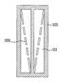
Translated fromKorean도 1은 종래 기술에 따른 액정표시소자의 평면도1 is a plan view of a conventional liquid crystal display
도 2a 내지 2f는 본 발명의 제 1 실시예에 따른 멀티 도메인 액정표시장치의 평면도2A to 2F are plan views of a multi-domain liquid crystal display device according to a first embodiment of the present invention.
도 3은 본 발명의 제 1 실시예에 따른 멀티 도메인 액정표시장치의 단면도3 is a cross-sectional view of a multi-domain liquid crystal display device according to the first embodiment of the present invention
도 4는 본 발명에 따른 액정형성방법을 설명하기 위한 도면4 is a view for explaining a liquid crystal forming method according to the present invention;
도 5a 내지 5d는 본 발명에 따른 전압(V)과 투과도(T)와 관계를 설명하기 위한 도면5A to 5D are diagrams for explaining the relation between the voltage (V) and the transmittance (T) according to the present invention
도 6a 내지 6e는 본 발명의 제 2 실시예에 따른 멀티 도메인 액정표시장치의 평면도6A to 6E are plan views of a multi-domain liquid crystal display device according to a second embodiment of the present invention
도 7a 및 7b는 도 6a의 Ⅰ-Ⅰ'선에 따른 단면도Figs. 7A and 7B are cross-sectional views taken along the line I-I '
도 8은 본 발명의 제 3 실시예에 따른 멀티 도메인 액정표시장치의 평면도8 is a plan view of a multi-domain liquid crystal display device according to a third embodiment of the present invention.
도 9a는 도 8의 Ⅱ-Ⅱ'선에 따른 단면도9A is a cross-sectional view taken along the line II-II '
도 9b는 도 8의 Ⅲ-Ⅲ'선에 따른 단면도9B is a cross-sectional view taken along the line III-III '
도면의 주요부분에 대한 부호의 설명DESCRIPTION OF THE REFERENCE NUMERALS
101 : 제 1 기판 101a : 제 2 기판101:
103 : 게이트 전극 105 : 게이트 절연막103: gate electrode 105: gate insulating film
106 : 반도체층 106a : 오믹콘택층106:
106b/106c : 소스/드레인 전극 106d : 데이터 배선106b / 106c: source /
107 : 보호막 109 : 슬릿(Slit) 패턴107: Protective film 109: Slit pattern
111 : 화소 전극 121 : 칼라 필터층111: pixel electrode 121: color filter layer
123 : 공통 전극 125 : 유전체 구조물123: common electrode 125: dielectric structure
131 : 위상차 필름 141 : 액정층131: retardation film 141: liquid crystal layer
200 : 씨일 패턴 202 : 액정200: seal pattern 202: liquid crystal
204 : 스페이서 300 : 홀(hole)204: spacer 300: hole
400,400a : 스토리지 커패시터의 제 1, 제 2 전극400, 400a: first and second electrodes of the storage capacitor
본 발명은 액정표시소자에 관한 것으로, 특히 멀티 도메인(Multi domain) 액정표시소자 및 그 제조방법에 관한 것이다.BACKGROUND OF THE INVENTION 1. Field of the Invention The present invention relates to a liquid crystal display device, and more particularly, to a multi-domain liquid crystal display device and a manufacturing method thereof.
최근, 액정을 배향하지 않고 화소 전극과 전기적으로 절연된 보조전극에 의해 액정을 구동하는 액정표시소자가 제안된 바 있다.In recent years, a liquid crystal display element has been proposed in which a liquid crystal is driven by an auxiliary electrode electrically insulated from the pixel electrode without orienting the liquid crystal.
즉, 도 1에 도시된 바와 같이, 제 1 기판 및 제 2 기판과, 제 1 기판 위에 종횡으로 배치되어 제 1 기판을 복수의 화소영역으로 구분하는 복수의 데이터 배선 및 게이트 배선과, 각각의 화소영역에 형성되는 박막트랜지스터(Thin Film Transistor :TFT)(여기서, 상기 박막트랜지스터는 게이트 전극, 게이트 절연막, 반도체층, 오믹콘택층(Ohmic contact layer) 및 소스/드레인 전극으로 구성됨)와, 상기 제 1 기판 전면에 걸쳐 형성된 보호막(37)과, 상기 보호막(37) 위에서 드레인 전극과 연결되는 화소 전극(13)과, 상기 게이트 절연막 위로 화소 전극(13)의 일부와 오버랩(Overlap)되도록 형성된 보조 전극(21)으로 구성된다.That is, as shown in Fig. 1, a liquid crystal display device includes a first substrate and a second substrate, a plurality of data wirings and gate wirings arranged vertically and horizontally on the first substrate to divide the first substrate into a plurality of pixel regions, A gate electrode, a gate insulating film, a semiconductor layer, an ohmic contact layer, and a source / drain electrode) formed in the first region, and a second thin film transistor (TFT) A
제 2 기판 위에는 상기 게이트 배선, 데이터 배선 및 박막트랜지스터로의 빛의 투과를 차단하는 차광층(25)과, 상기 차광층(25) 위에 형성된 칼라 필터층(23)과, 상기 칼라 필터층(23) 위에 형성된 공통 전극(17)이 형성되며 상기 제 1 기판과 제 2 기판과의 사이에 액정층이 형성된다.A
화소 전극(13)의 주변에 형성된 보조 전극(21)과 공통 전극(17)의 오픈영역(27)은 상기한 액정층에 인가되는 전기장을 왜곡시켜 단위 화소 내에서 액정분자를 다양하게 구동시킨다. 이것은 액정표시소자에 전압을 인가할 때, 왜곡된 전기장에 의한 유전 에너지가 액정 방향자를 원하는 방향으로 위치시킴을 의미한다.The
참고적으로, 도 1은 단위 화소만을 도시한 것이다.For reference, FIG. 1 shows only a unit pixel.
그러나 상기와 같은 종래 액정표시소자는 다음과 같은 문제점이 있었다.However, the conventional liquid crystal display device has the following problems.
첫째, 멀티 도메인 효과를 얻기 위해서는 공통 전극에 오픈 영역을 형성하여야 하며, 이를 위해 제조 공정 중 공통 전극에 오픈 영역을 형성하기 위한 추가 공정이 요구된다.First, in order to obtain a multi-domain effect, an open region must be formed in the common electrode. To this end, an additional process is required to form an open region in the common electrode during the manufacturing process.
둘째, 상기 오픈 영역을 형성하지 않거나 그 폭이 작으면, 도메인 분할에 필요한 전기장 왜곡 정도가 약하므로 액정의 방향자(Director)가 안정한 상태에 이르는 시간이 상대적으로 길어지게 되는 문제점이 발생한다.Secondly, if the open area is not formed or the width is small, the electric field distortion necessary for the domain division is weak, so that the time required for the director of the liquid crystal to reach a stable state becomes relatively long.
셋째, 오픈 영역에 의한 도메인 분할은 각 도메인마다 텍스쳐(Texture)가 불안정해지며, 이는 화질을 저하시키는 요인으로 작용한다.Third, in the domain segmentation by the open domain, the texture becomes unstable for each domain, which causes the degradation of the image quality.
넷째, 화소 전극과 보조 전극간의 전계가 강하게 걸림으로써 휘도가 증가하게 되고, 응답속도가 늦어지게 된다.Fourth, since the electric field between the pixel electrode and the auxiliary electrode is strong, the brightness is increased and the response speed is slowed down.
본 발명은 상기한 종래 기술의 문제점을 해결하기 위해 안출한 것으로, 공정을 간소화하고 화질을 개선시킬 수 있는 멀티 도메인 액정표시소자 및 그 제조방법을 제공하는데 그 목적이 있다.SUMMARY OF THE INVENTION The present invention has been made in order to solve the problems of the prior art described above, and it is an object of the present invention to provide a multi-domain liquid crystal display device and a manufacturing method thereof that can simplify a process and improve an image quality.
상기의 목적을 달성하기 위한 본 발명의 멀티 도메인 액정표시소자는 제 1 기판 및 제 2 기판과, 상기 제 1 기판 상에 종횡으로 배치되어 복수의 화소 영역을 정의하는 데이터 배선 및 게이트 배선과, 상기 각 화소 영역에 형성되며 복수의 슬릿 패턴을 갖는 화소 전극과, 상기 제 2 기판 상에 형성되며 복수의 도메인을 정의하기 위해 상기 화소 전극의 주변 및 그 내부에 상응하는 위치에 매트릭스 형태로 형성되는 유전체 구조물과, 상기 제 1 기판과 제 2 기판 사이에 형성된 액정층을 포함하여 구성되고, 그에 따른 제조방법은 제 1 기판 상에 게이트 배선 및 상기 게이트 배선과 교차하는 방향으로 데이터 배선을 형성하는 공정과, 상기 데이터 배선을 포함한 전면에 보호막을 형성하고, 상기 보호막 상에 투명도전막을 형성하는 공 정과, 상기 투명도전막을 패터닝하여 상기 게이트 배선과 데이터 배선에 의해 정의되는 화소 영역에 복수의 슬릿 패턴을 갖는 화소 전극을 형성하는 공정과, 상기 제 1 기판과 대향하는 제 2 기판상에 복수의 도메인을 정의하기 위해 상기 화소 전극의 주변 및 그 내부에 상응하는 위치에 매트릭스 형태의 유전체 구조물을 형성하는 공정과, 상기 제 1 기판과 제 2 기판 사이에 액정층을 형성하는 공정을 포함하여 이루어지는 것을 특징으로 한다.According to an aspect of the present invention, there is provided a multi-domain liquid crystal display device including a first substrate and a second substrate, a data line and a gate line arranged on the first substrate in a longitudinal direction and defining a plurality of pixel regions, A pixel electrode formed on each of the pixel regions and having a plurality of slit patterns; and a dielectric layer formed on the second substrate and formed in a matrix at a position corresponding to the periphery of the pixel electrode and the inside thereof to define a plurality of domains, And a liquid crystal layer formed between the first substrate and the second substrate. The manufacturing method includes a step of forming a gate wiring and a data wiring in a direction crossing the gate wiring on the first substrate, Forming a protective film on the entire surface including the data line and forming a transparent conductive film on the protective film, A step of forming a pixel electrode having a plurality of slit patterns in a pixel region defined by the gate wiring and the data wiring by patterning to form a pixel electrode on the second substrate opposite to the first substrate, Forming a dielectric structure in the form of a matrix at a position corresponding to the periphery of the electrode and the inside of the electrode; and forming a liquid crystal layer between the first substrate and the second substrate.
이와 같은 본 발명의 멀티 도메인 액정표시소자는 상판의 블랙 매트릭스(BM:Black Matrix)가 형성될 영역에 도메인 분할을 위한 유전체 구조물을 형성하고, 하판의 화소 전극에는 복수개의 슬릿 패턴(Slit pattern)을 형성하여 도메인 분할시 텍스쳐 안정화를 도모하는데 특징이 있다.In the multi-domain liquid crystal display device of the present invention, a dielectric structure for domain division is formed in a region where a black matrix (BM) of a top plate is to be formed, and a plurality of slit patterns And the texture is stabilized when the domain is divided.
한편, 본 발명의 다른 실시예에 따른 멀티 도메인 액정표시소자는 제 1 기판 및 제 2 기판과, 상기 제 1 기판 상에 종횡으로 배치되어 복수의 화소 영역을 정의하는 데이터 배선 및 게이트 배선과, 상기 각 화소 영역에 형성되며 복수개의 홀을 갖는 화소 전극과, 상기 제 2 기판 상에 형성되며 복수의 도메인을 정의하기 위해 상기 화소 전극의 주변 및 그 내부에 상응하는 위치에 매트릭스 형태로 형성되는 유전체 구조물과, 상기 제 1 기판과 제 2 기판 사이에 형성된 액정층을 포함하여 구성되고, 그에 따른 제조방법은 제 1 기판 상에 게이트 배선 및 상기 게이트 배선과 교차하는 방향으로 데이터 배선을 형성하는 공정과, 상기 데이터 배선을 포함한 전면에 보호막을 형성하고, 상기 보호막 상에 투명도전막을 형성하는 공정과, 상기 투명도전막을 패터닝하여 상기 게이트 배선과 데이터 배선에 의해 정의되는 화소 영역에 복수개의 홀을 갖는 화소 전극을 형성하는 공정과, 상기 제 1 기판과 대향하는 제 2 기판상에 복수의 도메인을 정의하기 위해 상기 화소 전극의 주변 및 그 내부에 상응하는 위치에 매트릭스 형태의 유전체 구조물을 형성하는 공정과, 상기 제 1 기판과 제 2 기판 사이에 액정층을 형성하는 공정을 포함하여 이루어지는 것을 특징으로 한다.According to another aspect of the present invention, there is provided a multi-domain liquid crystal display device including a first substrate and a second substrate, a data line and a gate line arranged vertically and horizontally on the first substrate to define a plurality of pixel regions, A pixel electrode formed in each pixel region and having a plurality of holes; a dielectric structure formed on the second substrate and formed in a matrix at a position corresponding to the periphery of the pixel electrode and the pixel electrode in order to define a plurality of domains, And a liquid crystal layer formed between the first substrate and the second substrate. The manufacturing method includes a step of forming a gate wiring and a data wiring in a direction crossing the gate wiring on the first substrate, Forming a protective film on the entire surface including the data line and forming a transparent conductive film on the protective film, Forming a pixel electrode having a plurality of holes in a pixel region defined by the gate wirings and the data wirings; and forming a plurality of pixel electrodes on the second substrate opposite to the first substrate, Forming a dielectric structure in the form of a matrix at a position corresponding to the periphery and the inside thereof; and forming a liquid crystal layer between the first substrate and the second substrate.
이와 같은 본 발명의 다른 실시예에 따른 멀티 도메인 액정표시소자는 상판의 블랙 매트릭스 영역에 유전체 구조물을 형성하고, 하판의 화소 전극에는 적어도 하나의 홀(hole)을 형성하여 공정을 간소화할 뿐 아니라 텍스쳐 안정화를 도모하는데 그 특징이 있다.The multi-domain liquid crystal display device according to another embodiment of the present invention has a structure in which a dielectric structure is formed in a black matrix region of a top plate and at least one hole is formed in a pixel electrode of a bottom plate, It is characterized by stabilization.
본 발명의 또 다른 실시예에 따른 멀티 도메인 액정표시소자는 제 1 기판 및 제 2 기판과, 상기 제 1 기판 상에 종횡으로 배치되어 복수의 화소 영역을 정의하는 데이터 배선 및 게이트 배선과, 상기 데이터 배선과 게이트 배선과의 교차부위에 형성된 U자 형상의 박막트랜지스터과, 상기 각 화소 영역에 형성되며 복수개의 홀 또는 슬릿 패턴을 갖는 화소 전극과, 상기 제 2 기판 상에 형성되며 복수의 도메인을 정의하기 위해 상기 화소 전극의 주변 및 그 내부에 상응하는 위치에 형성되는 매트릭스 형태의 유전체 구조물과, 상기 제 1 기판과 제 2 기판 사이에 형성된 액정층을 포함하여 구성되고, 그에 따른 제조방법은 제 1 기판 상에 박막트랜지스터를 형성하는 공정과, 상기 박막트랜지스터를 포함한 전면에 복수개의 홀 또는 슬릿 패턴을 갖는 화소 전극을 형성하는 공정과, 상기 제 1 기판과 대향하는 제 2 기판 상에 복수의 도메인을 정의하기 위해 상기 화소 전극의 주변 및 그 내부에 상 응하는 위치에 매트릭스 형태의 유전체 구조물을 형성하는 공정과, 상기 제 1 기판과 제 2 기판 사이에 액정층을 형성하는 공정을 포함하여 이루어진다.A multi-domain liquid crystal display device according to another embodiment of the present invention includes: a first substrate and a second substrate; a data wiring and a gate wiring arranged vertically and laterally on the first substrate to define a plurality of pixel regions; A pixel electrode formed on each of the pixel regions and having a plurality of holes or slit patterns; a plurality of pixel electrodes formed on the second substrate and defining a plurality of domains, And a liquid crystal layer formed between the first substrate and the second substrate. The method includes the steps of: forming a first substrate on a first substrate, A step of forming a thin film transistor on the thin film transistor, A step of forming a matrix-like dielectric structure at a position corresponding to the periphery of the pixel electrode and the inside thereof to define a plurality of domains on a second substrate facing the first substrate; And forming a liquid crystal layer between the first substrate and the second substrate.
여기서, 상기 박막트랜지스터는 상기 제 1 기판 상에 게이트 전극을 형성하는 공정과, 상기 게이트 전극을 포함한 전면에 게이트 절연막을 형성하는 공정과, 상기 게이트 전극 상부의 상기 게이트 절연막상에 반도체층 및 오믹콘택층을 형성하는 공정과, 상기 오믹콘택층상에 상기 화소 전극과 연결되는 드레인 전극 및 상기 드레인 전극을 U자 형상으로 에워싸는 소스전극을 형성하는 공정으로 이루어진다.The thin film transistor includes a step of forming a gate electrode on the first substrate, a step of forming a gate insulating film on the entire surface including the gate electrode, a step of forming a semiconductor layer and an ohmic contact on the gate insulating film over the gate electrode, And forming a drain electrode connected to the pixel electrode on the ohmic contact layer and a source electrode surrounding the drain electrode in a U-shape.
이와 같이 박막트랜지스터를 U자형으로 형성함으로써 플리커(flicker) 및 잔상해결을 도모하는데 특징이 있다.By forming the thin film transistor into a U-shape in this manner, flicker and afterimage are solved.
이하에서 본 발명의 멀티 도메인 액정표시소자 및 그 제조방법에 따른 바람직한 실시예를 보다 상세하게 설명하기로 한다.Hereinafter, preferred embodiments of a multi-domain liquid crystal display device and a manufacturing method thereof according to the present invention will be described in detail.
제 1 실시예First Embodiment
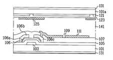
도 2a 내지 2f는 본 발명의 제 1 실시예에 따른 멀티 도메인 액정표시소자의 평면도이고, 도 3은 도 2a의 Ⅰ-Ⅰ'선에 따른 단면도이다. 참고적으로, 도 2a 내지 2f는 2-도메인, 3-도메인, 4-도메인으로 분할한 경우의 실시예를 도시한 것이며, 그 실시 형태는 반드시 도 2a 내지 2f로 한정되지는 않는다.FIGS. 2A to 2F are plan views of a multi-domain liquid crystal display device according to a first embodiment of the present invention, and FIG. 3 is a cross-sectional view taken along the line I-I 'of FIG. 2A. For reference, FIGS. 2A to 2F illustrate an embodiment in which a 2-domain, a 3-domain, and a 4-domain are divided, and the embodiment is not necessarily limited to FIGS.
도면에 도시된 바와 같이, 본 발명의 제 1 실시예에 따른 멀티 도메인 액정표시소자는 제 1 기판에 형성된 화소 전극(111)에 다수의 슬릿 패턴(109)을 형성하며, 한 화소를 복수개의 도메인으로 분할한 경우에는 각 도메인마다 다수의 슬릿 패턴(109)을 형성한다. 그리고 각 도메인의 주변을 따라 유전체 구조물(125)이 형성되는데, 상기 유전체 구조물(125)은 제 1 기판과 대향하는 제 2 기판의 공통 전극의 상부에 형성된다.As shown in the drawing, a multi-domain liquid crystal display device according to the first embodiment of the present invention includes a plurality of
이와 같은 본 발명 제 1 실시예에 따른 멀티 도메인 액정표시소자는 도 3에 도시한 바와 같이, 제 1 기판(101) 상에 게이트 전극(103)이 형성되고, 상기 게이트 전극(103)을 포함한 전면에 게이트 절연막(105)이 형성된다. 상기 게이트 절연막(105) 상에서 반도체층(106), 오믹콘택층(106a) 및 소스/드레인 전극(106b,106c)이 패터닝되어 박막트랜지스터(TFT)가 구성되며, 박막트랜지스터를 포함한 전면에 보호막(107)이 형성된다. 그리고 상기 보호막(107)을 통해 박막트랜지스터의 드레인 전극과 연결되는 복수개의 슬릿 패턴(109)(도 3에는 하나의 슬릿 패턴만이 도시됨)을 갖는 화소 전극(111)이 형성된다.3, the multi-domain liquid crystal display device according to the first embodiment of the present invention includes a
한편, 제 2 기판(101a) 상에는 색 표현을 위한 R, G, B 칼라 필터층(121)이 형성되고, 상기 칼라 필터층(121)을 포함한 전면에는 공통 전극(123)이 형성된다. 그리고 상기 화소 전극(111)을 제외한 영역으로 빛이 투과되는 것을 방지하기 위한 블랙 매트릭스가 형성될 영역에 상응하는 상기 공통 전극(123) 상에는 유전체 구조물(125)이 형성된다. 즉, 상기 유전체 구조물(125)은 화소 전극(111)의 주변 및 상기 화소 전극을 멀티 도메인으로 분할하였을 경우에는 각 도메인 경계 부위에 상응하는 공통 전극(123) 상에 형성하는 것으로, 화소 전극의 주변 및 내부에 형성하여 화소 영역을 복수의 도메인으로 분할한다.On the other hand, an R, G, and B
상기 제 1 기판(101)과 제 2 기판(101a) 중 적어도 한 기판의 배면에는 위상 차 필름(131)이 형성되며, 상기 제 1 기판(101)과 제 2 기판(101a) 사이에는 액정층(141)이 형성된다. 상기 액정층은 양(+) 또는 음(-)의 유전율 이방성을 가진 액정을 사용하며 카이랄 도펀트(chiral dopant)를 포함하는 것도 가능하다.A
한편, 상기 유전체 구조물(125)은 블랙수지, 예컨대 수지BM(black resin)으로 형성하므로 별도의 블랙 매트릭스가 필요치 않으며, 상기 블랙수지 이외에도 액정층의 유전율과 동일하거나 작은 유전율(dielectric constant)을 갖는 물질, 바람직하게는 유전율이 3 이하인 물질, 또는 아크릴(photoacrylate) 또는 BCB(Benzocyclobutene)와 같은 물질을 사용할 수도 있다.Since the
상기 위상차 필름(131)은 음성일축성 필름(negative uniaxial film)으로서, 광축이 하나인 일축성 물질로 형성하며, 기판에 수직인 방향과 시야각 변화에 따른 방향에서 사용자가 느끼는 시야각을 보상해 준다. 따라서, 계조 반전(Gray inversion)이 없는 영역을 넓히고, 경사방향에서 콘트라스트 비(Contrast ratio)를 높이며, 하나의 화소를 멀티 도메인으로 분할하는 것에 의해 더욱 효과적으로 좌우 방향의 시야각을 보상할 수 있다.The
한편, 상기 음성일축성 필름 이외에 위상차 필름으로서 음성이축성 필름(negative biaxial film)을 형성하여도 무방하며, 광축이 둘인 이축성 물질로 이루어진 음성이축성 필름은 상기한 일축성 필름에 비해 넓은 시야각 특성을 얻을 수 있다. 상기 위상차 필름은 적어도 하나의 기판에 일축성, 이축성 필름을 같이 형성할 수도 있으며, 하나의 기판에 일축성 필름 또는 이축성 필름을 각각 2장씩 형성할 수도 있다.On the other hand, a negative biaxial film may be formed as a phase difference film in addition to the negative uniaxial film, and a negative uniaxial film made of a biaxial substance having an optical axis twisted may have a wide viewing angle characteristic Can be obtained. The retardation film may be formed as a uniaxial or biaxial film on at least one substrate, or two uniaxial films or biaxial films may be formed on one substrate.
그리고 상기 위상차 필름을 부착한 후, 양 기판에는 편광자(polarizer)(도시하지 않음)를 부착할 수 있으며, 이 때, 편광자는 위상차 필름과 일체형으로 부착할 수도 있다.After attaching the retardation film, a polarizer (not shown) may be attached to both the substrates. In this case, the polarizer may be integrally attached to the retardation film.
이와 같이 구성된 본 발명의 제 1 실시예에 따른 멀티 도메인 액정표시소자를 제조하기 위해서는 우선, 제 1 기판(101)상에 게이트 전극(103), 게이트 절연막(105), 반도체층(106), 오믹콘택층(106a), 소스/드레인 전극(106b,106c)으로 이루어지는 박막트랜지스터(TFT) 및 박막트랜지스터의 드레인 전극(106c)과 연결되는 복수개의 슬릿 패턴(109)을 갖는 화소 전극(111)을 형성한다.In order to manufacture the multi-domain liquid crystal display device according to the first embodiment of the present invention, a
즉, Al, Mo, Cr, Ta 또는 Al합금 등과 같은 금속을 스퍼터링(Sputtering)법으로 형성한 후, 패터닝하여 게이트 배선(도시되지 않음) 및 게이트 전극(103)을 형성하고, 게이트 전극(103)을 포함한 기판 전면에 게이트 절연막(105)을 실리콘질화물(SiNX) 또는 실리콘산화물(SiOX)를 플라즈마 CVD(PECVD:Plasma Enhanced Chemical Vapor Deposition)법으로 형성한다.A gate wiring (not shown) and a
이때, 개구율을 향상시킬 목적으로 상기 게이트 절연막을 BCB(Benzocyclobutene), 아크릴 수지(Acrylic resin) 또는 폴리이미드(polyimide) 화합물 등으로 형성할 수도 있다.At this time, the gate insulating film may be formed of BCB (Benzocyclobutene), acrylic resin, or polyimide compound for the purpose of improving the aperture ratio.
이후, 게이트 절연막(105)상에 비정질 실리콘층과 n+비정질 실리콘층을 적층한 후 패터닝하여 반도체층(106) 및 오믹콘택층(106a)을 형성한다. 또한, 게이트 절연막 물질인 SiNx, 또는 SiOx, 비정질 실리콘층, n+비정질 실리콘층을 연속적으 로 증착한 후 게이트 절연막(105)을 형성하고, 비정질 실리콘층, n+비정질 실리콘층을 패터닝하여 반도체층(106) 및 오믹콘택층(106a)을 형성할 수도 있다.Thereafter, an amorphous silicon layer and an n+ amorphous silicon layer are stacked on the
그리고, Al, Mo, Cr, Ta 또는 Al합금 등과 같은 금속을 스퍼터링법으로 형성한 후 패터닝하여 상기 게이트 배선과 교차하는 방향으로 데이터 배선(도시되지 않음)을 형성하고, 상기 박막트랜지스터의 소스/드레인 전극(106b,106c)을 형성한다. Then, a metal such as Al, Mo, Cr, Ta, Al alloy or the like is formed by sputtering and patterned to form a data line (not shown) in a direction crossing the gate line,
이어서, 상기 소스/드레인 전극(106b,106c)을 포함한 전면에 BCB(Benzocyclobutene), 아크릴 수지(Acrylic resin) 또는 폴리이미드(polyimide) 화합물 또는 실리콘질화물, 실리콘산화물 등으로 보호막(107)을 형성한 후, ITO(Indium Tin Oxide)와 같은 투명한 도전성 물질을 형성한 후 패터닝하여 도 2a 내지 2f에 도시한 바와 같이, 각 도메인 내 화소 전극(111)에 복수개의 슬릿 패턴(109)을 형성한다.Subsequently, a
상기 슬릿 패턴(109)은 별도의 마스크를 이용하여 형성하는 것이 아니라 화소 전극(111)을 패터닝하기 위한 마스크에 슬릿 형태를 추가한 마스크를 이용하여 화소 전극과 동시에 형성하기 때문에 슬릿 패턴(109) 형성을 위한 별도의 마스크가 요구되지 않는다.Since the
한편, 제 2 기판(101a) 상에는 칼라 필터층(121)을 형성하고, 상기 칼라 필터층(121)을 포함한 전면에 ITO와 같은 투명도전막을 패터닝하여 공통 전극(123)을 형성한다. 이후, 도 2a 내지 2f에 도시된 것처럼 각 도메인을 정의하기 위해 매트릭스 형태의 유전체 구조물(125)을 형성한다.A
이때, 상기 유전체 구조물(125)은 블랙수지, 예컨대 수지BM(black resin)으로 형성하며, 화소 전극을 제외한 영역으로 빛이 투과되는 것을 방지하기 위한 블랙 매트릭스가 형성될 부위에 형성하므로, 별도의 블랙 매트릭스가 필요치 않다.At this time, the
한편 상기 유전체 구조물(125)의 물질은 상기 블랙수지 이외에도 액정층의 유전율과 동일하거나 작은 유전율(dielectric constant)을 갖는 물질, 바람직하게는 유전율이 3이하인 물질, 또는 아크릴(photoacrylate) 또는 BCB(Benzocyclobutene)와 같은 물질을 사용할 수도 있다.The material of the
이후, 제 1 기판(101)과 제 2 기판(101a)과의 사이에 액정층(141)을 형성하면, 본 발명 제 1 실시예에 따른 멀티 도메인 액정표시소자 제조공정이 완료된다.Thereafter, a
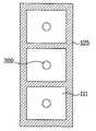
여기서, 상기 액정층(141)은 도 4에 도시한 바와 같이, 복수의 패턴들이 형성된 제 1 기판(101)과 제 2 기판(101a)을 준비한 후, 상기 제 1 기판(101) 상에 두 기판을 합착하기 위한 씨일 패턴(200)을 형성하고, 씨일 패턴(200)내에 일정량의 액정(202)을 적하방식으로 형성한다.4, the
그리고 제 2 기판(101a) 상에는 액정의 셀 갭(Cell gap)을 균일하게 유지하기 위한 스페이서(204)을 산포한 후, 상기 씨일 패턴(200)이 형성된 제 1 기판(101)과 상기 제 2 기판(101a)을 합착한 후, 자외선(UV) 또는 자외선과 열을 가하여 상기 씨일 패턴(200)을 경화시킨다.A
한편, 액정층을 형성하는 방법으로 전술한 감압상태에서 액정을 적하하는 방식 이외에 셀 내부를 진공으로 한 다음 그 압력차를 이용(모세관 현상)하여 액정이 셀 내부로 빨려 들어가도록 하는 방법 또는 일반적으로 널리 알려진 액정 주입 방 법 등 다양하게 적용할 수 있다. 상기 적하방식은 대면적 기판에 적용하면 액정형성시간을 감소시킬 수 있으며, 유전율 이방성이 음인 액정을 적용할 경우 액정의 점도가 높아 주입속도가 느린 점을 개선하는데 용이하게 적용할 수 있다. 또한, 스페이서는 패턴된 스페이서(columned spacer)를 이용하는 것도 가능하며, 씨일재로는 자외선 경화형 또는 상온에서 경화 가능한 씨일재 적용도 가능하다.On the other hand, in addition to a method of dropping the liquid crystal under the above-described reduced pressure state by the method of forming the liquid crystal layer, a method of making the inside of the cell vacuum and then using the pressure difference (capillary phenomenon) And the liquid crystal injection method widely known. The dropping method can reduce the liquid crystal formation time when applied to a large area substrate, and can be easily applied to improve the point that the liquid crystal has a high viscosity when the liquid crystal having a negative dielectric anisotropy is low, so that the injection speed is slow. The spacer may be a patterned spacer, and the sealant may be an ultraviolet curable sealant or a sealant that can be cured at room temperature.
여기서, 본 발명 제 1 실시예에 따른 멀티 도메인 액정표시소자는 제 1 기판(101) 및 제 2 기판(101a) 중 적어도 하나의 기판에 배향막(도시하지 않음)을 형성하는 것을 포함한다. 상기 배향막은 광반응성이 있는 물질 예컨대, PVCN(polyvinylcinnamate), PSCN(polysiloxanecinnamate) 또는 CelCN(cellulosecinnamate)계 화합물 등의 물질로 구성하여 광배향막을 형성할 수 있으며, 이외에도 광배향처리에 적합한 물질이면 어느 것이라도 무방하다.Here, the multi-domain liquid crystal display device according to the first embodiment of the present invention includes forming an alignment film (not shown) on at least one of the
상기 광배향막에는 광을 적어도 1회 조사하여 액정분자의 방향자가 이루는 프리틸트 각(pretilt angle) 및 배향 방향(alignment direction) 또는 프리틸트 방향(pretilt direction)을 동시에 결정하고, 그로 인한 액정의 배향 안정성을 확보한다. 이와 같은 광배향에 사용되는 광은 자외선 영역의 광이 적합하며, 비편광, 선편광 및 부분편광된 광 중에서 어느 것을 사용하여도 무방하다.The pretilt angle and the alignment direction or the pretilt direction of the liquid crystal molecules are determined simultaneously by irradiating the light to the photo alignment layer at least once to simultaneously determine the alignment stability of the liquid crystal . The light used in such a light alignment is suitable for light in the ultraviolet region, and any of unpolarized light, linearly polarized light and partially polarized light may be used.
그리고, 러빙처리하는 것도 가능하며, 그 배향막으로는 폴리이미드(polyimide), 폴리아미드(polyamide), PVA(polyvinylalcohol), 폴리아믹산(polyamic acid), 실리콘 산화물(SiOx) 등이 있으며, 그 밖의 러빙처리에 적합한 물질이라면 어떤 것이라도 적용 가능하다.Polyimide, polyamide, PVA (polyvinylalcohol), polyamic acid, silicon oxide (SiOx) and the like can be used as the alignment film. Other rubbing processes Any material that is suitable for the application is applicable.
그리고, 상기한 러빙법 또는 광배향법은 상기 제1기판 또는 제2기판 중 어느 한 기판에만 적용하거나 양 기판 모두에 처리하여도 되며, 양 기판에 서로 다른 배향처리를 하거나 배향막만 형성하고 배향처리를 하지 않는 것도 가능하다.The rubbing method or the photo alignment method may be applied to either one of the first substrate and the second substrate or may be performed on both substrates. Alternatively, both of the substrates may be subjected to different alignment processes or only an alignment film may be formed, It is also possible not to do.
이와 같이 배향처리를 함으로써 적어도 두 영역으로 분할된 멀티 도메인 액정표시소자를 형성하여 액정층의 액정분자가 각 영역 상에서 서로 상이하게 배향하도록 할 수 있다. 또한, 각 영역에서 전 영역을 비배향영역으로 하여도 되고, 영역 중 적어도 하나의 영역을 비배향처리하는 것도 가능하다.By performing the alignment treatment in this manner, the multi-domain liquid crystal display elements divided into at least two regions can be formed, so that the liquid crystal molecules of the liquid crystal layer can be oriented differently on the respective regions. In addition, the entire region may be a non-alignment region in each region, or at least one region of the regions may be subjected to a non-alignment treatment.
한편, 도 5a 내지 5d는 본 발명의 멀티 도메인 액정표시소자에 따른 전압과 투과도와의 관계를 도시한 것으로, 보다 바람직하게는 도 2c에 도시된 구조의 화소 전극을 예로 한 것이다.5A to 5D show the relationship between the voltage and the transmittance according to the multi-domain liquid crystal display device of the present invention, and more preferably, the pixel electrode having the structure shown in FIG. 2C is taken as an example.
도 5a는 화소 전극에 0V의 전압을 인가하였을 경우의 단위 화소를 도시한 것으로, 전체적으로 빛의 투과가 없는 블랙 상태를 보여주고, 도 5b는 3V의 전압을 인가하였을 경우, 화소 전극이 복수개의 도메인으로 분할되고, 각 도메인마다 4개의 서브 도메인으로 분할되는 것을 보여주며, 도 5c 및 도 5d로 갈수록 빛의 투과량이 증가하여 고휘도의 화질을 구현할 수 있음을 보여준다.FIG. 5A shows a unit pixel when a voltage of 0V is applied to the pixel electrode. FIG. 5B shows a black state without light transmission as a whole, FIG. 5B shows a case where a voltage of 3V is applied, And it is divided into four sub-domains for each domain. It is shown that the amount of light transmitted increases with increasing distance to the sub-domains of FIG. 5C and FIG. 5D, thereby realizing a high-luminance image quality.
여기서, 상기 각 도메인은 도면에는 명확하게 나타나지 않았지만, 제 2 기판(101a)의 공통전극 상에 형성된 유전체 구조물(125)에 의해 분할된다.Here, each of the domains is divided by a
이와 같은 본 발명의 제 1 실시예에 따른 멀티 도메인 액정표시소자 및 그 제조방법에 따르면, 제 1 기판상의 화소 전극(111)에 복수개의 슬릿 패턴(109)을 형성하고, 제 2 기판상의 공통전극 상에 도메인 분할을 위한 유전체 구조물(125)을 형성하여 각 도메인마다 텍스쳐를 안정화시키고, 멀티 도메인을 구현하기 위한 추가적인 공정이 필요치 않으므로 보다 간단한 공정으로 멀티 도메인을 구현할 수 있다. 또한, 액정을 적하방식으로 형성하기 때문에 액정주입 시간을 절약할 수 있고, 액정 주입에 따른 오염의 정도를 최소화하여 신뢰성을 향상시킬 수 있다.According to the multi-domain liquid crystal display element and the method of manufacturing the same according to the first embodiment of the present invention, a plurality of
제 2 실시예Second Embodiment
본 발명의 제 2 실시예는 상판의 블랙 매트릭스 영역에 유전체 구조물을 형성하고, 하판의 화소 전극에는 복수개의 홀(hole)을 형성하여 텍스쳐(texture) 안정화를 도모하고 공정을 간소화하는데 그 특징이 있다.The second embodiment of the present invention is characterized in that a dielectric structure is formed in a black matrix region of a top plate and a plurality of holes are formed in a pixel electrode of a lower panel to achieve texture stabilization and simplify the process .
먼저, 도 6a 내지 6e는 본 발명 제 2 실시예에 따른 멀티 도메인 액정표시소자의 평면도로써, 상판(제 2 기판)에 형성된 유전체 구조물(125)과 하판(제 1 기판)에 복수개의 홀(hole)(300)을 화소 전극(111)을 도시한 것으로서, 그 실시 형태는 반드시 도 6a 내지 6e로 한정되지는 않는다.6A to 6E are plan views of a multi-domain liquid crystal display device according to a second embodiment of the present invention. The
도 7a는 본 발명 제 2 실시예에 따른 멀티 도메인 액정표시소자의 단면도로서, 도 6a의 Ⅰ-Ⅰ'선에 따른 단면도이고, 도 7b는 화소 전극에 형성된 홀이 게이트 절연막(105)까지 연장된 예를 보여준다.7A is a cross-sectional view of the multi-domain liquid crystal display device according to the second embodiment of the present invention, taken along the line I-I 'in FIG. 6A. FIG. 7B is a cross- Show examples.
도 7a에 도시한 바와 같이, 제 1 기판(101) 상에는 게이트 전극(103)이 형성되고, 상기 게이트 전극(103)을 포함한 전면에 게이트 절연막(105)이 형성된다. 상기 게이트 절연막(105) 상에는 반도체층(106), 오믹콘택층(106a) 및 소스/드레인 전극(106b,106c)이 패터닝되고, 상기 소스/드레인 전극(106b,106c)을 포함한 전면에 보호막(107)이 형성되며, 상기 보호막(107)을 통해 드레인 전극(106c)과 연결되 며 복수개의 홀(300)을 갖는 화소 전극(111)이 형성된다.7A, a
제 2 기판(101a) 상에는 색 표현을 위한 R, G, B 칼라 필터층(121)이 형성되고, 상기 칼라 필터층(121)을 포함한 전면에는 공통 전극(123)이 형성된다. 그리고 상기 화소 전극(111)을 제외한 영역으로 빛이 투과되는 것을 방지하기 위한 블랙 매트릭스가 형성될 영역의 상기 공통 전극(123) 상에는 유전체 구조물(125)이 형성된다.The R, G, and B color filter layers 121 for color representation are formed on the
한편, 도 7b에서와 같이, 홀(300)이 보호막(107)에 국한되지 않고, 그 하부의 게이트 절연막(105)까지 형성하는 것도 가능하다. 참고로, 도 7b는 홀이 형성된 위치를 제외하고는 도 7a와 동일하다.On the other hand, as shown in FIG. 7B, the
이와 같이 구성된 본 발명의 제 2 실시예에 따른 멀티 도메인 액정표시소자를 제조하기 위해서는 우선, 제 1 기판(101)상에 게이트 배선(103) 및 각 화소 영역에 게이트 전극(103), 게이트 절연막(105), 반도체층(106), 오믹콘택층(106a) 및 소스/드레인 전극(106b,106c)으로 이루어지는 박막 트랜지스터(TFT)를 형성한다.In order to manufacture the multi-domain liquid crystal display device according to the second embodiment of the present invention, a
즉, Al, Mo, Cr, Ta 또는 Al합금 등과 같은 금속을 스퍼터링(Sputtering)법으로 형성한 후, 패터닝하여 게이트 배선(도시되지 않음) 및 게이트 전극(103)을 형성한 후, 그 위에 게이트 절연막(105)을 실리콘질화물(SiNX) 또는 실리콘산화물(SiOX)를 플라즈마 CVD(PECVD:Plasma Enhanced Chemical Vapor Deposition)법으로 형성한다.That is, a metal such as Al, Mo, Cr, Ta, or an Al alloy is formed by a sputtering method and then patterned to form a gate wiring (not shown) and a
이때, 개구율을 향상시킬 목적으로 상기 게이트 절연막(105)을 BCB(Benzocyclobutene), 아크릴 수지(Acrylic resin) 또는 폴리이미드(polyimide) 화합물 등으로 형성할 수도 있다.At this time, the
이후, 게이트 절연막상에 비정질 실리콘층과 n+비정질 실리콘층을 적층한 후 패터닝하여 반도체층(106) 및 오믹콘택층(106a)을 형성한다. 또한, 게이트 절연막 물질인 SiNx, 또는 SiOx, 비정질 실리콘층, n+비정질 실리콘층을 연속적으로 증착한 후 게이트 절연막(105)을 형성하고, 비정질 실리콘층, n+비정질 실리콘층을 패터닝하여 반도체층(106) 및 오믹콘택층(106a)을 형성할 수도 있다.Thereafter, an amorphous silicon layer and an n+ amorphous silicon layer are stacked on the gate insulating layer and then patterned to form the
그리고, Al, Mo, Cr, Ta 또는 Al합금 등과 같은 금속을 스퍼터링법으로 형성한 후 패터닝하여 데이터 배선 및 소스/드레인 전극(106b,106c)을 형성한다.Then, a metal such as Al, Mo, Cr, Ta or an Al alloy is formed by a sputtering method and then patterned to form a data wiring and source /
이어서, 상기 소스/드레인 전극(106b,106c)을 포함한 전면에 BCB(Benzocyclobutene), 아크릴 수지(Acrylic resin) 또는 폴리이미드(polyimide) 화합물 또는 실리콘질화물, 실리콘산화물 등으로 보호막(107)을 형성한 후, ITO(Indium Tin Oxide)와 같은 투명한 도전성 물질을 형성한 후 패터닝하여 화소 전극(111)을 형성함과 동시에 도 6a 내지 6e에 도시한 바와 같이, 멀티 도메인을 구현하기 위해 각 도메인 내 화소 전극(111)에 복수개의 홀(300)을 형성한다.Subsequently, a
상기 홀(300)은 별도의 마스크를 이용하여 형성하는 것이 아니라 화소 전극(111)을 패터닝하기 위한 마스크에 홀(hole) 형태를 추가한 마스크를 이용하여 화소 전극과 동시에 형성하기 때문에 홀을 형성하기 위한 별도의 마스크가 요구되지 않는다.The
한편, 제 2 기판(101a) 상에는 칼라 필터층(121)을 형성하고, 상기 칼라 필터층(121)을 포함한 전면에 ITO와 같은 투명도전막을 패터닝하여 공통 전극(123)을 형성한다. 이후, 도 6a 내지 6e에 도시된 바와 같이, 각 도메인을 정의하기 위해 매트릭스 형태의 유전체 구조물(125)을 형성한다.A
이때, 상기 유전체 구조물(125)은 블랙수지, 예컨대 수지BM(black resin)으로 형성한다. 따라서 별도의 블랙 매트릭스가 필요치 않으며, 상기 블랙수지 이외에도 액정층의 유전율과 동일하거나 작은 유전율(dielectric constant)을 갖는 물질, 바람직하게는 유전율이 3이하인 물질, 또는 아크릴(photoacrylate) 또는 BCB(Benzocyclobutene)와 같은 물질을 사용할 수도 있다.At this time, the
이후, 제 1 기판(101)과 제 2 기판(101a)과의 사이에 액정층(141)을 형성하면, 본 발명 제 2 실시예에 따른 멀티 도메인 액정표시소자 제조공정이 완료된다.Thereafter, when the
이와 같은 본 발명의 제 2 실시예는 전술한 제 1 실시예와 비교하여 화소 전극에 슬릿 패턴(109)이 형성된 대신에 홀(300)이 형성된 것을 제외하고는 본 발명 제 1 실시예와 그 구조 및 제조 공정이 동일하므로 이하에서 생략한다.The second embodiment of the present invention is similar to the first embodiment of the present invention except that the
제 3 실시예Third Embodiment
본 발명의 제 3 실시예는 박막트랜지스터의 구조를 제외하고, 화소 전극에 복수개의 슬릿 패턴 또는 복수개의 홀을 갖는 본 발명 제 1 실시예 및 제 2 실시예와 그 구조 및 제조공정이 동일하다.The third embodiment of the present invention is the same in structure and manufacturing process as the first and second embodiments of the present invention, except for the structure of the thin film transistor, in which the pixel electrode has a plurality of slit patterns or a plurality of holes.
도 8은 본 발명의 제 3 실시예에 따른 멀티 도메인 액정표시소자의 평면도이다.8 is a plan view of a multi-domain liquid crystal display device according to a third embodiment of the present invention.
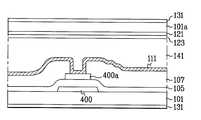
도 8에 도시한 바와 같이, 본 발명 제 3 실시예는 교차 배치되는 게이트 배선(103a) 및 데이터 배선(106d)과, 상기 게이트 배선(103a)과 데이터 배선(106d)의 교차 부위에 형성된 U자 형상의 박막트랜지스터(TFT)와, 상기 박막트랜지스터(TFT)와 연결되며, 복수개의 홀(300)을 갖는 화소 전극(111)과, 상기 화소 전극(111)의 주변을 따라 형성된 유전체 구조물(125)로 구성된다.8, the third embodiment of the present invention is characterized in that a
여기서, 상기 홀(300) 대신에 슬릿 패턴을 형성할 수도 있으며, 홀(300)을 형성한 경우에는 본 발명 제 2 실시예의 도 7a 및 도 7b에 도시된 바와 같이, 홀(300)을 보호막(107)까지 형성하거나 또는 게이트 절연막(105)까지 형성할 수도 있다. 그리고, 슬릿 패턴을 형성할 경우 화소 전극(111)의 형태는 본 발명 제 1 실시예의 도 3에 도시한 화소 전극(111)과 동일하다.In this case, a slit pattern may be formed in place of the
상기 게이트 배선(103a) 및 데이터 배선(106d) 그리고 박막트랜지스터(TFT) 및 화소 전극(111)은 제 1 기판(101)상에 형성되고, 상기 유전체 구조물(125)은 상기 제 1 기판(101)과 대향하는 제 2 기판(101a)상에 형성되며, 그 중에서도 블랙 매트릭스가 형성될 영역에 상응하여 공통전극의 상부에 형성된다.The
이와 같은 본 발명의 제 3 실시예를 보다 상세하게 설명하면 다음과 같다.The third embodiment of the present invention will be described in detail as follows.
도 9a는 도 8의 Ⅱ-Ⅱ'선에 따른 단면이고, 도 9b는 도 8의 Ⅲ-Ⅲ'선에 따른 단면도로서, 도 9a 및 9b에 도시한 바와 같이, 제 1 기판(101) 상에 Al, Mo, Cr, Ta 또는 Al합금 등과 같은 금속을 스퍼터링(Sputtering)법으로 형성한 후, 패터닝하여 게이트 배선(103a), 게이트 전극(103) 및 스토리지 커패시터의 제 1 전극(400)을 형성하고, 게이트 전극(103)을 포함한 기판 전면에 게이트 절연막(105)을 실리콘질화물(SiNX) 또는 실리콘산화물(SiOX)를 플라즈마 CVD(PECVD:Plasma Enhanced Chemical Vapor Deposition)법으로 형성한다.9A is a cross-sectional view taken along the line II-II 'in FIG. 8, and FIG. 9B is a cross-sectional view taken along line III-III' in FIG. 8. As shown in FIGS. 9A and 9B, A metal such as Al, Mo, Cr, Ta, Al alloy or the like is formed by a sputtering method and then patterned to form the
이때, 개구율을 향상시킬 목적으로 상기 게이트 절연막(105)을 BCB(Benzocyclobutene), 아크릴 수지(Acrylic resin) 또는 폴리이미드(polyimide) 화합물 등으로 형성할 수도 있다.At this time, the
이후, 게이트 절연막(105)상에 비정질 실리콘층과 n+비정질 실리콘층을 적층한 후 패터닝하여 반도체층(106) 및 오믹콘택층(106a)을 형성한다. 또한, 게이트 절연막 물질인 SiNx, 또는 SiOx, 비정질 실리콘층, n+비정질 실리콘층을 연속적으로 증착한 후 게이트 절연막(105)을 형성하고, 비정질 실리콘층, n+비정질 실리콘층을 패터닝하여 반도체층(106) 및 오믹콘택층(106a)을 형성할 수도 있다.Thereafter, an amorphous silicon layer and an n+ amorphous silicon layer are stacked on the
그리고, Al, Mo, Cr, Ta 또는 Al합금 등과 같은 금속을 스퍼터링법으로 형성한 후 패터닝하여 상기 게이트 배선(103a)과 교차하는 방향으로 데이터 배선(106d)을 형성하고, 상기 박막트랜지스터의 드레인 전극(106c) 및 상기 드레인 전극(106c)을 U자 형상으로 에워싸는 소스 전극(106b) 그리고 스토리지 커패시터의 제 2 전극(400a)을 형성한다.A metal such as Al, Mo, Cr, Ta, Al alloy or the like is formed by a sputtering method and patterned to form a
이어서, 상기 소스/드레인 전극(106b,106c) 및 스토리지 커패시터의 제 2 전극(400a)을 포함한 전면에 BCB(Benzocyclobutene), 아크릴 수지(Acrylic resin) 또는 폴리이미드(polyimide) 화합물 또는 실리콘질화물, 실리콘산화물 등으로 보호막(107)을 형성한 후, ITO(Indium Tin Oxide)와 같은 투명한 도전성 물질을 형 성한 후 패터닝하여 각 도메인내 복수개의 홀(300) 또는 슬릿 패턴을 갖는 화소 전극(111)을 형성한다.Next, a BCB (benzocyclobutene), an acrylic resin or a polyimide compound or a silicon nitride, a silicon oxide, or a silicon oxide is deposited on the entire surface including the source /
여기서, 상기 홀(300) 또는 슬릿 패턴은 별도의 마스크를 이용하여 형성하는 것이 아니라 화소 전극(111)을 패터닝하기 위한 마스크에 홀(hole) 또는 슬릿(Slit) 형태를 추가한 마스크를 이용하여 화소 전극과 동시에 형성하기 때문에 별도의 마스크가 요구되지 않는다.Here, the
그리고 상기 화소 전극(111)은 콘택홀을 통해 스토리지 커패시터의 제 2 전극(400a)과 연결된다.The
한편, 제 2 기판(101a) 상에는 칼라 필터층(121)을 형성하고, 상기 칼라 필터층(121)을 포함한 전면에 ITO와 같은 투명도전막을 패터닝하여 공통 전극(123)을 형성한다. 이후, 도 2a 내지 2f에 도시된 것처럼 각 도메인을 정의하기 위해 매트릭스 형태의 유전체 구조물(125)을 형성한다.A
이때, 상기 유전체 구조물(125)은 블랙수지, 예컨대 수지BM(black resin)으로 형성하며, 화소 전극(111)을 제외한 영역으로 빛이 투과되는 것을 방지하기 위한 블랙 매트릭스가 형성될 부위에 형성하므로, 별도의 블랙 매트릭스가 필요치 않다.At this time, the
한편 상기 유전체 구조물(125)의 물질은 상기 블랙수지 이외에도 액정층의 유전율과 동일하거나 작은 유전율(dielectric constant)을 갖는 물질, 바람직하게는 유전율이 3이하인 물질, 또는 아크릴(photoacrylate) 또는 BCB(Benzocyclobutene)와 같은 물질을 사용할 수도 있다.The material of the
이후, 제 1 기판(101)과 제 2 기판(101a)과의 사이에 액정층(141)을 형성하면, 본 발명 제 3 실시예에 따른 멀티 도메인 액정표시소자 제조공정이 완료된다.Then, a
이와 같은 본 발명의 제 3 실시예는 박막트랜지스터의 구조를 제외한 다른 부분에서 있어서는 본 발명 제 1 실시예와 동일하다.The third embodiment of the present invention is the same as the first embodiment except for the structure of the thin film transistor.
이상 상술한 바와 같이, 본 발명의 멀티 도메인 액정표시소자 및 그 제조방법은 다음과 같은 효과가 있다.INDUSTRIAL APPLICABILITY As described above, the multi-domain liquid crystal display element of the present invention and its manufacturing method have the following effects.
첫째, 별도의 마스크 및 공정의 추가 없이 멀티 도메인 효과를 얻을 수 있으므로 공정을 간소화할 수 있다.First, since a multi-domain effect can be obtained without adding a separate mask and a process, the process can be simplified.
둘째, 화소 전극에 슬릿 또는 오픈 영역을 형성하여 각 도메인마다 텍스쳐(Texture)의 안정을 도모하여 화질을 개선시킬 수 있다.Secondly, a slit or an open region is formed in the pixel electrode, so that the texture can be stabilized for each domain and the image quality can be improved.
셋째, 액정 주입시간을 단축하여 전체 공정에 요구되는 시간을 절약하고, 그로 인한 오염 물질의 혼입을 방지하여 신뢰성이 높은 소자를 제조할 수 있다.
Third, the liquid crystal injection time can be shortened to save the time required for the entire process, and contamination of contaminants can be prevented, thereby making it possible to manufacture a highly reliable device.
Claims (16)
Translated fromKoreanPriority Applications (3)
| Application Number | Priority Date | Filing Date | Title |
|---|---|---|---|
| KR1020000052329AKR100685914B1 (en) | 2000-09-05 | 2000-09-05 | Multi-domain liquid crystal display device and manufacturing method thereof |
| US09/944,116US7212268B2 (en) | 2000-09-05 | 2001-09-04 | Multi-domain liquid crystal display device and method for manufacturing the same |
| US11/730,863US7834970B2 (en) | 2000-09-05 | 2007-04-04 | Multi-domain liquid crystal display device and method for manufacturing the same |
Applications Claiming Priority (1)
| Application Number | Priority Date | Filing Date | Title |
|---|---|---|---|
| KR1020000052329AKR100685914B1 (en) | 2000-09-05 | 2000-09-05 | Multi-domain liquid crystal display device and manufacturing method thereof |
Publications (2)
| Publication Number | Publication Date |
|---|---|
| KR20020019185A KR20020019185A (en) | 2002-03-12 |
| KR100685914B1true KR100685914B1 (en) | 2007-02-23 |
Family
ID=19687376
Family Applications (1)
| Application Number | Title | Priority Date | Filing Date |
|---|---|---|---|
| KR1020000052329AExpired - Fee RelatedKR100685914B1 (en) | 2000-09-05 | 2000-09-05 | Multi-domain liquid crystal display device and manufacturing method thereof |
Country Status (2)
| Country | Link |
|---|---|
| US (2) | US7212268B2 (en) |
| KR (1) | KR100685914B1 (en) |
Cited By (1)
| Publication number | Priority date | Publication date | Assignee | Title |
|---|---|---|---|---|
| KR101006781B1 (en)* | 2003-12-30 | 2011-01-10 | 엘지디스플레이 주식회사 | Liquid crystal display device and manufacturing method thereof |
Families Citing this family (15)
| Publication number | Priority date | Publication date | Assignee | Title |
|---|---|---|---|---|
| US7079210B2 (en)* | 2001-11-22 | 2006-07-18 | Samsung Electronics Co., Ltd. | Liquid crystal display and thin film transistor array panel |
| KR20030042221A (en)* | 2001-11-22 | 2003-05-28 | 삼성전자주식회사 | a thin film transistor array panel for a liquid crystal display |
| KR100906635B1 (en)* | 2002-10-23 | 2009-07-10 | 삼성전자주식회사 | Liquid crystal display |
| JP3879727B2 (en)* | 2003-10-02 | 2007-02-14 | セイコーエプソン株式会社 | Liquid crystal display device and electronic device |
| KR100987725B1 (en)* | 2003-12-12 | 2010-10-13 | 삼성전자주식회사 | Array substrate, manufacturing method thereof and liquid crystal display device having same |
| TWI358830B (en)* | 2003-12-12 | 2012-02-21 | Samsung Electronics Co Ltd | Array substrate, method of manufacturing the same |
| JP4293038B2 (en)* | 2004-04-15 | 2009-07-08 | セイコーエプソン株式会社 | Liquid crystal device and electronic device |
| KR101061856B1 (en)* | 2004-11-03 | 2011-09-02 | 삼성전자주식회사 | Thin film transistor array panel |
| KR20070068891A (en)* | 2005-12-27 | 2007-07-02 | 엘지.필립스 엘시디 주식회사 | Liquid crystal display having in-cell backlight and manufacturing method thereof |
| KR20070103543A (en)* | 2006-04-19 | 2007-10-24 | 삼성전자주식회사 | Liquid crystal display |
| JP4254855B2 (en)* | 2006-12-20 | 2009-04-15 | ソニー株式会社 | Liquid crystal display device and manufacturing method thereof |
| TWI368097B (en)* | 2007-10-17 | 2012-07-11 | Hannstar Display Corp | Liquid crystal display panels, pixels, and switch elements |
| KR101146985B1 (en)* | 2010-03-11 | 2012-05-23 | 삼성모바일디스플레이주식회사 | Display device and method of manufacturing the same |
| KR102331178B1 (en)* | 2015-04-02 | 2021-11-26 | 삼성디스플레이 주식회사 | Display device |
| CN108121116A (en)* | 2017-12-29 | 2018-06-05 | 深圳市华星光电半导体显示技术有限公司 | A kind of alignment method of liquid crystal display panel |
Citations (4)
| Publication number | Priority date | Publication date | Assignee | Title |
|---|---|---|---|---|
| KR19980025831A (en)* | 1996-10-05 | 1998-07-15 | 김광호 | Manufacturing method of liquid crystal display device |
| KR100186555B1 (en)* | 1996-05-15 | 1999-05-01 | 구자홍 | Lcd device driving method |
| KR19990072150A (en)* | 1996-10-16 | 1999-09-27 | 야스카와 히데아키 | Liquid crystal device substrate, liquid crystal device and projection display device |
| JP2012137227A (en)* | 2010-12-27 | 2012-07-19 | Fujitsu General Ltd | Air conditioner |
Family Cites Families (25)
| Publication number | Priority date | Publication date | Assignee | Title |
|---|---|---|---|---|
| US4691995A (en) | 1985-07-15 | 1987-09-08 | Semiconductor Energy Laboratory Co., Ltd. | Liquid crystal filling device |
| JPH06235925A (en) | 1993-02-10 | 1994-08-23 | Matsushita Electric Ind Co Ltd | Manufacture of liquid crystal display element |
| JPH08101395A (en) | 1994-09-30 | 1996-04-16 | Matsushita Electric Ind Co Ltd | Liquid crystal display element manufacturing method |
| US5532180A (en)* | 1995-06-02 | 1996-07-02 | Ois Optical Imaging Systems, Inc. | Method of fabricating a TFT with reduced channel length |
| JPH0961829A (en) | 1995-08-21 | 1997-03-07 | Matsushita Electric Ind Co Ltd | Liquid crystal display element manufacturing method |
| KR100364771B1 (en)* | 1995-10-20 | 2003-04-07 | 엘지전자 주식회사 | Liquid crystal display and method for fabricating the same |
| US5731216A (en)* | 1996-03-27 | 1998-03-24 | Image Quest Technologies, Inc. | Method of making an active matrix display incorporating an improved TFT |
| JPH10177178A (en) | 1996-12-17 | 1998-06-30 | Matsushita Electric Ind Co Ltd | Manufacturing method of liquid crystal display element |
| JPH10333157A (en) | 1997-06-03 | 1998-12-18 | Matsushita Electric Ind Co Ltd | Manufacturing method of liquid crystal display device |
| JPH10333159A (en) | 1997-06-03 | 1998-12-18 | Matsushita Electric Ind Co Ltd | Liquid crystal display |
| JP3935246B2 (en)* | 1997-08-18 | 2007-06-20 | エルジー フィリップス エルシーディー カンパニー リミテッド | Liquid crystal display |
| JPH11133438A (en) | 1997-10-24 | 1999-05-21 | Matsushita Electric Ind Co Ltd | Liquid crystal display device and its manufacturing method |
| JPH11142864A (en) | 1997-11-07 | 1999-05-28 | Matsushita Electric Ind Co Ltd | Manufacturing method of liquid crystal display device |
| EP0929104B1 (en)* | 1998-01-09 | 2009-08-05 | Sony Corporation | Electroluminescence device and process for producing the same |
| JPH11248930A (en) | 1998-03-06 | 1999-09-17 | Matsushita Electric Ind Co Ltd | Color filter substrate, method of manufacturing the color filter substrate, and liquid crystal display device using the color filter substrate |
| JPH11326922A (en) | 1998-05-14 | 1999-11-26 | Matsushita Electric Ind Co Ltd | Liquid crystal display panel manufacturing method |
| US5917199A (en)* | 1998-05-15 | 1999-06-29 | Ois Optical Imaging Systems, Inc. | Solid state imager including TFTS with variably doped contact layer system for reducing TFT leakage current and increasing mobility and method of making same |
| GB2343012B (en)* | 1998-10-19 | 2003-05-28 | Lg Philips Lcd Co Ltd | A multi-domain liquid crystal display device |
| US6255130B1 (en)* | 1998-11-19 | 2001-07-03 | Samsung Electronics Co., Ltd. | Thin film transistor array panel and a method for manufacturing the same |
| US6900869B1 (en)* | 1998-11-25 | 2005-05-31 | Lg. Philips Lcd Co., Ltd. | Multi-domain liquid crystal display device with particular dielectric structures |
| JP2001222017A (en)* | 1999-05-24 | 2001-08-17 | Fujitsu Ltd | Liquid crystal display device and method of manufacturing the same |
| KR100480814B1 (en)* | 1999-12-31 | 2005-04-06 | 엘지.필립스 엘시디 주식회사 | Multi-domain liquid crystal display device |
| KR20010082831A (en)* | 2000-02-21 | 2001-08-31 | 구본준, 론 위라하디락사 | Method of Fabricating Liquid Crystal Display Device |
| JP3678974B2 (en)* | 2000-03-29 | 2005-08-03 | 富士通ディスプレイテクノロジーズ株式会社 | Manufacturing method of liquid crystal display device |
| KR100587365B1 (en)* | 2000-08-08 | 2006-06-08 | 엘지.필립스 엘시디 주식회사 | Multi-domain liquid crystal display device |
- 2000
- 2000-09-05KRKR1020000052329Apatent/KR100685914B1/ennot_activeExpired - Fee Related
- 2001
- 2001-09-04USUS09/944,116patent/US7212268B2/ennot_activeExpired - Lifetime
- 2007
- 2007-04-04USUS11/730,863patent/US7834970B2/ennot_activeExpired - Fee Related
Patent Citations (4)
| Publication number | Priority date | Publication date | Assignee | Title |
|---|---|---|---|---|
| KR100186555B1 (en)* | 1996-05-15 | 1999-05-01 | 구자홍 | Lcd device driving method |
| KR19980025831A (en)* | 1996-10-05 | 1998-07-15 | 김광호 | Manufacturing method of liquid crystal display device |
| KR19990072150A (en)* | 1996-10-16 | 1999-09-27 | 야스카와 히데아키 | Liquid crystal device substrate, liquid crystal device and projection display device |
| JP2012137227A (en)* | 2010-12-27 | 2012-07-19 | Fujitsu General Ltd | Air conditioner |
Non-Patent Citations (4)
| Title |
|---|
| 1001865550000 * |
| 1019980025831 * |
| 1019990072150 * |
| 12137227 * |
Cited By (1)
| Publication number | Priority date | Publication date | Assignee | Title |
|---|---|---|---|---|
| KR101006781B1 (en)* | 2003-12-30 | 2011-01-10 | 엘지디스플레이 주식회사 | Liquid crystal display device and manufacturing method thereof |
Also Published As
| Publication number | Publication date |
|---|---|
| US7212268B2 (en) | 2007-05-01 |
| KR20020019185A (en) | 2002-03-12 |
| US7834970B2 (en) | 2010-11-16 |
| US20070247561A1 (en) | 2007-10-25 |
| US20020039161A1 (en) | 2002-04-04 |
Similar Documents
| Publication | Publication Date | Title |
|---|---|---|
| KR100313949B1 (en) | Multi-domain Liquid Crystal Display Device | |
| JP4171145B2 (en) | Multi-domain liquid crystal display device | |
| US6654090B1 (en) | Multi-domain liquid crystal display device and method of manufacturing thereof | |
| US7834970B2 (en) | Multi-domain liquid crystal display device and method for manufacturing the same | |
| US20010019388A1 (en) | Multi-domain liquid crystal display device | |
| KR20030048865A (en) | Multi domain Liquid Crystal Display Device | |
| KR100587365B1 (en) | Multi-domain liquid crystal display device | |
| US7079211B2 (en) | Multi-domain liquid crystal display compromising field induction windows having patterns different from each other in at least two of the pixel regions | |
| KR100323735B1 (en) | Multi-domain liquid crystal display device | |
| US6525794B1 (en) | Multi-domain liquid crystal display device having a dielectric frame controlling alignment of the liquid crystal molecules | |
| KR100357217B1 (en) | Multi-domain liquid crystal display device | |
| KR100244537B1 (en) | A liquid crystal display device | |
| US6850300B2 (en) | Multi-domain liquid crystal display device with particular dielectric frames | |
| KR20010073422A (en) | Multi-domain liquid crystal display device | |
| KR100487425B1 (en) | Multi-domain liquid crystal display device | |
| KR100323734B1 (en) | Multi-domain liquid crystal display device | |
| KR100327443B1 (en) | Multi-domain liquid crystal display device | |
| KR100769178B1 (en) | Multi-domain liquid crystal display device and manufacturing method thereof | |
| KR100313948B1 (en) | Multi-domain liquid crystal display device | |
| KR100595297B1 (en) | Multi-domain liquid crystal display device and manufacturing method thereof | |
| KR100853770B1 (en) | Multi-domain liquid crystal display device | |
| KR20030097513A (en) | Multi domain Liquid Crystal Display Device | |
| KR20030048868A (en) | Multi domain Liquid Crystal Display Device | |
| KR20030057769A (en) | Multi domain Liquid Crystal Display Device | |
| KR20040003326A (en) | Multi domain Liquid Crystal Display Device |
Legal Events
| Date | Code | Title | Description |
|---|---|---|---|
| PA0109 | Patent application | St.27 status event code:A-0-1-A10-A12-nap-PA0109 | |
| PN2301 | Change of applicant | St.27 status event code:A-3-3-R10-R13-asn-PN2301 St.27 status event code:A-3-3-R10-R11-asn-PN2301 | |
| PG1501 | Laying open of application | St.27 status event code:A-1-1-Q10-Q12-nap-PG1501 | |
| A201 | Request for examination | ||
| AMND | Amendment | ||
| P11-X000 | Amendment of application requested | St.27 status event code:A-2-2-P10-P11-nap-X000 | |
| P13-X000 | Application amended | St.27 status event code:A-2-2-P10-P13-nap-X000 | |
| PA0201 | Request for examination | St.27 status event code:A-1-2-D10-D11-exm-PA0201 | |
| E902 | Notification of reason for refusal | ||
| PE0902 | Notice of grounds for rejection | St.27 status event code:A-1-2-D10-D21-exm-PE0902 | |
| AMND | Amendment | ||
| E13-X000 | Pre-grant limitation requested | St.27 status event code:A-2-3-E10-E13-lim-X000 | |
| P11-X000 | Amendment of application requested | St.27 status event code:A-2-2-P10-P11-nap-X000 | |
| P13-X000 | Application amended | St.27 status event code:A-2-2-P10-P13-nap-X000 | |
| E601 | Decision to refuse application | ||
| PE0601 | Decision on rejection of patent | St.27 status event code:N-2-6-B10-B15-exm-PE0601 | |
| J201 | Request for trial against refusal decision | ||
| PJ0201 | Trial against decision of rejection | St.27 status event code:A-3-3-V10-V11-apl-PJ0201 | |
| AMND | Amendment | ||
| P11-X000 | Amendment of application requested | St.27 status event code:A-2-2-P10-P11-nap-X000 | |
| P13-X000 | Application amended | St.27 status event code:A-2-2-P10-P13-nap-X000 | |
| PB0901 | Examination by re-examination before a trial | St.27 status event code:A-6-3-E10-E12-rex-PB0901 | |
| E902 | Notification of reason for refusal | ||
| PE0902 | Notice of grounds for rejection | St.27 status event code:A-1-2-D10-D21-exm-PE0902 | |
| P11-X000 | Amendment of application requested | St.27 status event code:A-2-2-P10-P11-nap-X000 | |
| P13-X000 | Application amended | St.27 status event code:A-2-2-P10-P13-nap-X000 | |
| B701 | Decision to grant | ||
| PB0701 | Decision of registration after re-examination before a trial | St.27 status event code:A-3-4-F10-F13-rex-PB0701 | |
| GRNT | Written decision to grant | ||
| PR0701 | Registration of establishment | St.27 status event code:A-2-4-F10-F11-exm-PR0701 | |
| PR1002 | Payment of registration fee | St.27 status event code:A-2-2-U10-U11-oth-PR1002 Fee payment year number:1 | |
| PG1601 | Publication of registration | St.27 status event code:A-4-4-Q10-Q13-nap-PG1601 | |
| PN2301 | Change of applicant | St.27 status event code:A-5-5-R10-R13-asn-PN2301 St.27 status event code:A-5-5-R10-R11-asn-PN2301 | |
| PR1001 | Payment of annual fee | St.27 status event code:A-4-4-U10-U11-oth-PR1001 Fee payment year number:4 | |
| R18-X000 | Changes to party contact information recorded | St.27 status event code:A-5-5-R10-R18-oth-X000 | |
| PR1001 | Payment of annual fee | St.27 status event code:A-4-4-U10-U11-oth-PR1001 Fee payment year number:5 | |
| R18-X000 | Changes to party contact information recorded | St.27 status event code:A-5-5-R10-R18-oth-X000 | |
| PR1001 | Payment of annual fee | St.27 status event code:A-4-4-U10-U11-oth-PR1001 Fee payment year number:6 | |
| R18-X000 | Changes to party contact information recorded | St.27 status event code:A-5-5-R10-R18-oth-X000 | |
| FPAY | Annual fee payment | Payment date:20121228 Year of fee payment:7 | |
| PR1001 | Payment of annual fee | St.27 status event code:A-4-4-U10-U11-oth-PR1001 Fee payment year number:7 | |
| FPAY | Annual fee payment | Payment date:20131227 Year of fee payment:8 | |
| PR1001 | Payment of annual fee | St.27 status event code:A-4-4-U10-U11-oth-PR1001 Fee payment year number:8 | |
| FPAY | Annual fee payment | Payment date:20150127 Year of fee payment:9 | |
| PR1001 | Payment of annual fee | St.27 status event code:A-4-4-U10-U11-oth-PR1001 Fee payment year number:9 | |
| FPAY | Annual fee payment | Payment date:20160128 Year of fee payment:10 | |
| PR1001 | Payment of annual fee | St.27 status event code:A-4-4-U10-U11-oth-PR1001 Fee payment year number:10 | |
| FPAY | Annual fee payment | Payment date:20170116 Year of fee payment:11 | |
| PR1001 | Payment of annual fee | St.27 status event code:A-4-4-U10-U11-oth-PR1001 Fee payment year number:11 | |
| PR1001 | Payment of annual fee | St.27 status event code:A-4-4-U10-U11-oth-PR1001 Fee payment year number:12 | |
| LAPS | Lapse due to unpaid annual fee | ||
| PC1903 | Unpaid annual fee | St.27 status event code:A-4-4-U10-U13-oth-PC1903 Not in force date:20190216 Payment event data comment text:Termination Category : DEFAULT_OF_REGISTRATION_FEE | |
| PC1903 | Unpaid annual fee | St.27 status event code:N-4-6-H10-H13-oth-PC1903 Ip right cessation event data comment text:Termination Category : DEFAULT_OF_REGISTRATION_FEE Not in force date:20190216 |