KR100685455B1 - Flipper ring device for semiconductor manufacturing process - Google Patents
Flipper ring device for semiconductor manufacturing processDownload PDFInfo
- Publication number
- KR100685455B1 KR100685455B1KR1020050042627AKR20050042627AKR100685455B1KR 100685455 B1KR100685455 B1KR 100685455B1KR 1020050042627 AKR1020050042627 AKR 1020050042627AKR 20050042627 AKR20050042627 AKR 20050042627AKR 100685455 B1KR100685455 B1KR 100685455B1
- Authority
- KR
- South Korea
- Prior art keywords
- support frame
- link
- guide rail
- rotary
- manufacturing process
- Prior art date
- Legal status (The legal status is an assumption and is not a legal conclusion. Google has not performed a legal analysis and makes no representation as to the accuracy of the status listed.)
- Expired - Fee Related
Links
Images


Classifications
- B—PERFORMING OPERATIONS; TRANSPORTING
- B65—CONVEYING; PACKING; STORING; HANDLING THIN OR FILAMENTARY MATERIAL
- B65G—TRANSPORT OR STORAGE DEVICES, e.g. CONVEYORS FOR LOADING OR TIPPING, SHOP CONVEYOR SYSTEMS OR PNEUMATIC TUBE CONVEYORS
- B65G47/00—Article or material-handling devices associated with conveyors; Methods employing such devices
- B65G47/22—Devices influencing the relative position or the attitude of articles during transit by conveyors
- B—PERFORMING OPERATIONS; TRANSPORTING
- B65—CONVEYING; PACKING; STORING; HANDLING THIN OR FILAMENTARY MATERIAL
- B65H—HANDLING THIN OR FILAMENTARY MATERIAL, e.g. SHEETS, WEBS, CABLES
- B65H5/00—Feeding articles separated from piles; Feeding articles to machines
- B65H5/08—Feeding articles separated from piles; Feeding articles to machines by grippers, e.g. suction grippers
- B65H5/12—Revolving grippers, e.g. mounted on arms, frames or cylinders
- H—ELECTRICITY
- H01—ELECTRIC ELEMENTS
- H01L—SEMICONDUCTOR DEVICES NOT COVERED BY CLASS H10
- H01L21/00—Processes or apparatus adapted for the manufacture or treatment of semiconductor or solid state devices or of parts thereof
- H01L21/02—Manufacture or treatment of semiconductor devices or of parts thereof
Landscapes
- Engineering & Computer Science (AREA)
- Mechanical Engineering (AREA)
- Physics & Mathematics (AREA)
- Condensed Matter Physics & Semiconductors (AREA)
- General Physics & Mathematics (AREA)
- Manufacturing & Machinery (AREA)
- Computer Hardware Design (AREA)
- Microelectronics & Electronic Packaging (AREA)
- Power Engineering (AREA)
- Container, Conveyance, Adherence, Positioning, Of Wafer (AREA)
Abstract
Translated fromKoreanDescription
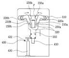
Translated fromKorean도1은 본 발명의 제1실시예에 따른 반도체 제조공정용 플립퍼링장치를 나타내는 사시도이며,1 is a perspective view showing a flippering apparatus for a semiconductor manufacturing process according to a first embodiment of the present invention;
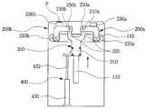
도2는 도1에 도시된 반도체 제조공정용 플립퍼링장치의 구성요소들을 나타내는 분해사시도이며,FIG. 2 is an exploded perspective view illustrating components of a flippering apparatus for a semiconductor manufacturing process shown in FIG. 1;
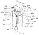
도3a 및 도3b는 각각 도1에 도시된 플립퍼링장치가 로터리형 픽커에 적용된 경우의 배치관계를 나타내는 사시도 및 평면도이며,3A and 3B are respectively a perspective view and a plan view showing an arrangement relationship when the flippering device shown in Fig. 1 is applied to a rotary picker;
도4a 내지 도4f는 도1에 도시된 플립퍼링장치의 작동상태를 나타내는 정면도들이며,4A to 4F are front views illustrating an operating state of the flipping device shown in FIG.
도5는 본 발명의 제2실시예에 따른 반도체 제조공정용 플립퍼링장치를 나타내는 사시도이며,5 is a perspective view showing a flippering apparatus for a semiconductor manufacturing process according to a second embodiment of the present invention;
도6은 도5에 도시된 플립퍼링장치가 직선형 픽커에 적용된 경우의 배치관계를 나타내는 사시도이며,FIG. 6 is a perspective view showing an arrangement relationship when the flippering device shown in FIG. 5 is applied to a straight picker; FIG.
도7은 본 발명의 제3실시예에 따른 반도체 제조공정용 플립퍼링장치를 나타내는 분해사시도이며,7 is an exploded perspective view showing a flippering apparatus for a semiconductor manufacturing process according to a third embodiment of the present invention;
도8은 본 발명의 제4실시예에 따른 반도체 제조공정용 플립퍼링장치를 나타 내는 사시도이며,8 is a perspective view showing a flippering apparatus for a semiconductor manufacturing process according to a fourth embodiment of the present invention;
도9는 도8에 도시된 플립퍼링장치를 나타내는 정면도이며,FIG. 9 is a front view of the flipping device shown in FIG. 8;
도10은 도8에 도시된 플립퍼링장치가 로터리형 픽커에 적용된 경우의 배치관계를 나타내는 사시도이며,FIG. 10 is a perspective view showing an arrangement relationship when the flippering device shown in FIG. 8 is applied to a rotary picker; FIG.
도11은 본 발명의 제5실시예에 따른 반도체 제조공정용 플립퍼링장치를 나타내는 사시도이다.11 is a perspective view showing a flippering device for a semiconductor manufacturing process according to the fifth embodiment of the present invention.
*도면의 주요 부분에 대한 부호의 설명** Description of the symbols for the main parts of the drawings *
100 : 지지프레임110 : 작동홈100: support frame 110: working groove
200a,200b : 제1 및 제2회전레버210a,210b : 제1 및 제2힌지부200a, 200b: first and second rotation levers 210a, 210b: first and second hinge parts
220a,220b : 제1 및 제2베어링230a,230b : 제1 및 제2흡착헤드220a, 220b: First and second bearing 230a, 230b: First and second suction head
240a,240b : 제1 및 제2안착부250a,250b : 제1 및 제2힌지축240a, 240b: first and
300 : 작동링크310 : 링크본체(부)300: operation link 310: link body (part)
320 : 체결부(재)400 : 링크이동수단320: fastening part (re) 400: link moving means
410 : 가이드레일420 : 이동블럭410: guide rail 420: moving block
430 : 구동실린더432 : 실린더로드430: driving cylinder 432: cylinder rod
500 : 픽커P : 패키지500: Picker P: Package
본 발명은 반도체 제조공정용 플립퍼링장치에 관한 것으로서, 더욱 상세하게는 반도체 패키지 등의 피가공물을 용이하게 뒤집을 수 있는 반도체 제조공정용 플립퍼링장치에 관한 것이다.BACKGROUND OF THE INVENTION 1. Field of the Invention The present invention relates to a flippering device for a semiconductor manufacturing process, and more particularly, to a flippering device for a semiconductor manufacturing process that can easily reverse a workpiece such as a semiconductor package.
일반적으로 반도체 패키지는 스트립 형태로 몰딩, 트리밍, 포밍, 싱귤레이션 등 여러 공정을 통해 개별화된 유닛으로 제조된다. 이러한 반도체 패키지는 여러 공정을 거치는 동안 그 특성 및 제조 공정에 따라 공정 전, 후에 뒤집혀져야 할 경우가 발생한다. 예를 들어, 패키지의 일측면에 마킹을 해야하거나, 비젼검사 또는 전기적인 테스트가 수행되어야 하거나, 후공정과의 연계작업을 위해 가공이 끝난 패키지가 트레이, 튜브, 릴 등에 뒤집혀져 적재되어야 하는 경우 등을 들 수 있다. 이와 같은 플립퍼링장치는 반도체 제조공정 중 패키지 등의 피가공물을 역전시키는데 사용되는 장치로서, 통상 온로딩장치와 가공/검사장치 사이에 별도로 설치되거나 가공/검사장치와 오프로딩장치 사이에 설치된다.In general, semiconductor packages are manufactured as individual units in strip form through various processes such as molding, trimming, forming and singulation. Such a semiconductor package needs to be flipped before and after the process, depending on its characteristics and manufacturing process during various processes. For example, if one side of the package needs to be marked, vision inspection or electrical test should be performed, or the finished package should be loaded upside down on trays, tubes, reels, etc. Etc. can be mentioned. Such a flippering device is a device used for reversing a workpiece such as a package during a semiconductor manufacturing process, and is usually installed separately between an onloading device and a processing / inspecting device or between a processing / inspecting device and an offloading device.
한편, 이러한 플립퍼링장치로는 피가공물을 부착한 상태에서 180도 회전하여 피가공물을 역전시킨 후 픽커로 진공흡착하는 방식 등 다양한 구조가 개시되어 있다. 그러나, 이러한 종래의 플립퍼링장치는 그 구성이 복잡하고 피가공물의 처리속도가 느리다는 문제점들이 있었다.On the other hand, such a flippering device is disclosed a variety of structures, such as a method of rotating the workpiece to 180 degrees in the state attached to the workpiece to reverse the workpiece and then vacuum-adsorbed with a picker. However, such a conventional flippering device has a problem in that its configuration is complicated and the processing speed of a workpiece is slow.
본 발명은 상기와 같은 종래의 제반 문제점들을 해소하기 위해 제안된 것으로, 본 발명의 목적은 개별의 반도체 패키지 등의 피가공물을 용이하게 역전시킬 수 있는 구조를 가진 플립퍼링장치를 제공하는 것이다.SUMMARY OF THE INVENTION The present invention has been proposed to solve the above conventional problems, and an object of the present invention is to provide a flippering device having a structure capable of easily reversing a workpiece such as an individual semiconductor package.
상기와 같은 목적을 달성하기 위하여 본 발명에 따른 플립퍼링장치는 지지프레임과, 상기 지지프레임에 각 일단이 설치되며, 그 상면에 피가공물이 안착되는 제1 및 제2안착부가 각각 형성된 제1 및 제2회전레버와, 상기 제1 및 제2회전레버의 각 타단이 회전 가능하게 고정되며, 수직 이동가능하게 설치된 작동링크와, 상기 지지프레임에 결합되어 상기 작동링크를 수직 이동시키는 링크이동수단을 포함한다.In order to achieve the above object, the flippering device according to the present invention includes a support frame and a first end of each of which is installed on the support frame, the first and second seats of which a workpiece is mounted on the upper surface of the first and second seats, respectively. A second rotation lever, an operation link rotatably fixed to the other end of the first and second rotation levers, vertically movable, and link moving means coupled to the support frame to vertically move the operation link; Include.
상기 작동링크는 상방향으로 'U'자 형태로 분기된 체결부를 가지며, 상기 제1 및 제2회전레버는 일측으로 돌출된 제1 및 제2힌지부를 가지며, 상기 제1 및 제2힌지부는 상기 체결부 각 단부와 회전 가능하게 체결된다.The actuating link has a fastening portion branched in a 'U' shape in an upward direction, and the first and second rotary levers have first and second hinge portions protruding to one side, and the first and second hinge portions are The fastening part is rotatably fastened to each end.
상기 제1 및 제2안착부는 피가공물과 대응되는 형상이며 상기 제1 및 제2회전레버의 힌지축을 기준으로 소정 각도로 틀어지게 형성된다.The first and second seating portions may be shaped to correspond to the workpiece, and may be twisted at a predetermined angle with respect to the hinge axes of the first and second rotary levers.
상기 지지프레임에는 수평방향으로 작동홈이 형성되며, 상기 제1 및 제2회전레버의 각 일단에는 상기 작동홈에 삽입되어 수평 이동되는 베어링이 구비된다.An operation groove is formed in the support frame in a horizontal direction, and each end of the first and second rotation levers includes a bearing inserted into the operation groove to move horizontally.
또한, 상기 지지프레임은 서로 대칭되게 배치된 제1 및 제2프레임으로 구성되며, 상기 제1 및 제2프레임에는 수평방향으로 제1 및 제2작동홈이 각각 형성되며, 상기 제1 및 제2회전레버의 각 일단 양측면에는 상기 제1 및 제2작동홈에 삽입되어 수평 이동되는 한 쌍의 베어링이 구비될 수 있다.In addition, the support frame is composed of first and second frames arranged symmetrically to each other, the first and second frame is formed with first and second operating grooves in the horizontal direction, respectively, the first and second Each end of each of the rotary levers may be provided with a pair of bearings which are inserted into the first and second operating grooves and are horizontally moved.
또한, 상기 지지프레임에는 수평방향으로 수평가이드레일이 설치되며, 상기 제1 및 제2회전레버의 각 일단에는 상기 수평가이드레일을 따라 수평 이동되는 제1 및 제2가이드부재가 회전 가능하게 각각 구비될 수 있다.In addition, the support frame is provided with a horizontal guide rail in a horizontal direction, each end of the first and second rotary levers are provided with a rotatable first and second guide members that are horizontally moved along the horizontal guide rail, respectively. Can be.
상기 링크이동수단은 상기 지지프레임에 수직 방향으로 연장 형성된 가이드레일과, 상기 작동링크가 고정되며, 상기 가이드레일에 수직 이동가능하게 삽입 설치된 이동블럭과, 상기 지지프레임에 고정되며, 상기 이동블럭에 수직 이동력을 제공하는 구동실린더를 포함한다.The link moving means includes a guide rail extending in a direction perpendicular to the support frame, a movable block fixed to the operation link and inserted into the guide rail so as to be vertically movable, and fixed to the support frame, And a drive cylinder that provides vertical movement force.
또한, 상기 링크이동수단은 상기 지지프레임에 설치된 구동모터와, 상기 구동모터에 회전 가능하게 결합된 회전판과, 그 일단은 상기 회전판의 일측에 결합되며, 그 타단은 상기 작동링크에 결합된 크랭크축과, 상기 지지프레임에 수직 방향으로 연장 형성된 가이드레일과, 상기 작동링크가 고정되며, 상기 가이드레일에 수직 이동가능하게 삽입 설치된 이동블럭을 포함한다.In addition, the link moving means is a drive motor installed in the support frame, a rotary plate rotatably coupled to the drive motor, one end thereof is coupled to one side of the rotary plate, the other end is a crank shaft coupled to the operation link And a guide rail extending in the vertical direction to the support frame, and a movable block fixed to the operation link and inserted into the guide rail so as to be vertically movable.
이하, 본 발명의 제1실시예에 따른 플립퍼링장치를 첨부된 도면을 참조하여 상세히 설명한다.Hereinafter, a flipping device according to a first embodiment of the present invention will be described in detail with reference to the accompanying drawings.
본 발명에 따른 실시예들의 구성요소들을 설명함에 있어, 다른 실시예에서 이미 설명된 구성요소에 대해서는 상세한 설명을 생략하며, 대칭적으로 배치된 구성요소에 대해서는 어느 일방을 중심으로 설명하기로 한다. 또한, 본 발명에 의해 처리되는 피가공물로는 반도체 패키지를 상정하여 설명하지만, 반도체 스트립 기타 반도체제품도 피가공물로 처리될 수 있음을 미리 밝혀둔다. 또한, 구성요소들의 작동상태를 설명함에 있어, 도면에 도시된 방향을 중심으로 상하좌우 또는 회전방향을 결정하기로 한다.In describing the components of the embodiments according to the present invention, detailed descriptions of the components already described in other embodiments will be omitted, and symmetrically arranged components will be described with reference to any one of them. In addition, the workpiece to be processed by the present invention is described assuming a semiconductor package, it will be appreciated that the semiconductor strip and other semiconductor products can also be processed into the workpiece. In addition, in describing the operating states of the components, it will be determined up, down, left and right or the direction of rotation based on the direction shown in the drawings.
도1은 본 발명의 제1실시예에 따른 반도체 제조공정용 플립퍼링장치를 나타 내는 사시도이며, 도2는 도1에 도시된 반도체 제조공정용 플립퍼링장치의 구성요소들을 나타내는 분해사시도이며, 도3은 도1에 도시된 플립퍼링장치가 로터리형 픽커에 적용된 경우의 배치관계를 나타내는 사시도이다.1 is a perspective view showing a flippering device for a semiconductor manufacturing process according to a first embodiment of the present invention, Figure 2 is an exploded perspective view showing the components of the flippering device for a semiconductor manufacturing process shown in FIG. 3 is a perspective view showing an arrangement relationship when the flippering device shown in FIG. 1 is applied to a rotary picker.
도1 내지 도3에 도시된 바와 같이, 본 발명의 제1실시예에 따른 반도체 제조공정용 플립퍼링장치는 지지프레임(100), 제1 및 제2회전레버(200a,200b), 작동링크(300) 및 링크이동수단(400)으로 구성된다.1 to 3, the flippering apparatus for a semiconductor manufacturing process according to the first embodiment of the present invention, the
상기 지지프레임(100)은 다른 구성요소들을 지지하는 요소이다. 상기 지지프레임(100)의 일측면에는 수평방향으로 작동홈(110)이 형성되어 있다.The
상기 제1회전레버(200a)는 온로딩장치(미도시)로부터 전달된 패키지를 전달받는 요소이며, 상기 제2회전레버(200b)는 상기 제1회전레버(200a)로부터 패키지를 전달받아 오프로딩장치(미도시)로 전달하는 요소이다. 도1 및 도2에 도시된 바와 같이, 상기 제1 및 제2회전레버(200a,200b)는 서로 대칭되게 배치되어 있다. 상기 제1 및 제2회전레버(200a,200b)는 전체적으로 'ㄱ'자 형상으로써, 그 일단에는 상기 작동링크(300)에 제1 및 제2힌지부(210a,210b)가 구비되어 있으며, 그 타단 일측면에는 상기 작동홈(110)에 삽입되어 수평 이동되는 제1 및 제2베어링(220a,220b)이 각각 구비되어 있다. 한편, 본 실시예에서는 이러한 제1 및 제2베어링(220a,220b)이 원통 형상의 롤러베어링으로 설계되어 있으나, 설계조건에 따라 다양한 구조의 롤러베어링 또는 미끄럼베어링으로 설계변경될 수 있다.The
또한, 상기 제1 및 제2회전레버(200a,200b)의 상부에는 제1 및 제2흡착헤드(230a,230b)가 돌출 형성되어 있으며, 상기 제1 및 제2흡착헤드(230a,230b)의 상면에는 패키지가 안착되는 제1 및 제2안착부(240a,240b)가 각각 형성되어 있다. 상기 제1 및 제2안착부(240a,240b)는 패키지와 동일한 형상이거나 패키지를 흡착할 수 있도록 오링이나 사각패드를 사용하는 것도 가능하다. 참고로 본 실시예에서는 도3a 및 도3b에 도시된 바와 같이, 상기 제1 및 제2안착부(240a,240b)는 사각형 홈 형상으로 서로 직교하는 제1변(L1)과 제2변(L2)으로 구성되어 있다. 상기 제1 및 제2안착부(240a,240b)는 상기 제1 및 제2회전레버(200a,200b)의 힌지축(250a,250b)을 기준으로 소정 각도로 틀어지게 형성되어 있다. 이는 로터리형 픽커(500)로 패키지를 온로딩 및 오프로딩시킬 경우 패키지를 용이하게 내려놓거나 집어올리기 위한 것으로, 소정 각도는 로터리형 픽커(500)의 원주방향과 평행한 각도를 의미한다. 다시 말하면, 상기 제1 및 제2안착부(240a,240b)는 피가공물을 온로딩 및 오프로딩시키는 로터리형 픽커(500)의 중심과 상기 제1 또는 제2안착부(240a,240b)의 중심을 연결하는 선(L3)과 상기 제1 및 제2안착부(240a,240b)의 제1변(L1)이 서로 직교하도록 배치되어 있다.In addition, first and
한편, 도시되지 않았지만, 상기 제1 및 제2안착부(240a,240b)에는 서로 독립적으로 제어되며 상기 제1 및 제2안착부(240a,240b)로 진공흡착력을 제공하는 제1 및 제2진공라인이 각각 형성되어 있다. 이러한 제1진공라인은 상기 제1 및 제2안착부(240a,240b)가 서로 맞물리는 경우 상기 제1안착부(240a)에 안착된 패키지를 분리시키도록 진공 압출력을 부여하며, 상기 제2진공라인은 상기 제1안착부(240a)로부터 이탈된 패키지가 상기 제2안착부(240b)에 흡착되도록 진공 흡입력을 부여한다. 따라서, 반도체 패키지는 제1회전레버(200a)의 제1안착부(240a)에서 제2회전레버(200b)의 제2안착부(240b)로 이동되면서 역전된다.On the other hand, although not shown, the first and
상기 작동링크(300)는 상기 제1 및 제2회전레버(200a,200b)를 회전시키는 요소이다. 이러한 작동링크(300)는 링크본체부(310)와, 상기 링크본체부(310)로부터 상방향으로 'U'자 형태로 분기된 체결부(320)로 구성되어 있다. 이러한 체결부(320)의 단부는 제1 및 제2힌지핀(250a,250b)에 의해 상기 제1 및 제2힌지부(210a,210b)에 회전 가능하게 체결되어 있다. 즉, 상기 작동링크(300)가 하방향으 로 이동하면 상기 제1 및 제2회전레버(200a,200b)는 각각 반시계방향 및 시계방향으로 회전하여 상기 제1 및 제2안착부(240a,240b)가 서로 맞물리게 되고, 상기 작동링크(300)가 상방향으로 이동하면 상기 제1 및 제2회전레버(200a,200b)는 각각 시계방향 및 반시계방향으로 회전하여 상기 제1 및 제2안착부(240a,240b)가 상부에 위치된다.The
상기 링크이동수단(400)은 상기 지지프레임(100)에 수직 방향으로 연장 형성된 가이드레일(410)과, 상기 가이드레일(410)에 수직 이동가능하게 삽입 설치된 이동블럭(420)과, 상기 이동블럭(420)에 수직 이동력을 제공하는 구동실린더(430)로 구성되어 있다. 상기 이동블럭(420)의 배면에는 상기 가이드레일(410)에 삽입되는 가이드홈(미도시)이 형성되어 있으며, 상기 이동블럭(420)의 정면에는 상기 작동링크(300)의 링크본체부(310)가 고정되어 있다. 또한, 상기 구동실린더(430)는 상기 지지프레임(100)에 고정되어 있으며, 이동가능하게 설치된 실린더로드(432)에 의해 상기 이동블럭(420)을 상하 이동시킨다.The link moving means 400 includes a
한편, 본 실시예에서는 제1 및 제2흡착헤드(230a,230b)의 상면 각각에 하나의 안착부가 형성된 예가 도시되어 있으나, 설계조건에 따라서는 제1 및 제2흡착헤드(230a,230b)의 상면 각각에 상기 제1 및 제2힌지축(250a,250b) 방향으로 2개 이상의 안착부를 형성하여 한번에 여러 개의 패키지를 역전시키도록 구성될 수도 있을 것이다. 또한 본 실시예에서는 제1 및 제2흡착헤드(230a,230b)의 상이 평면인 예가 도시되어 있으나, 설계조건에 따라서 소정 반경으로 라운드진 형태로 구성될 수 있을 것이다. 또한, 설계조건에 따라 구동실린더(430) 대신에 스탭모터, 리니어 모터, 솔레노이드 액추에이터, 서보모터 등 공지의 구동수단들이 선택될 수 있다.Meanwhile, in the present embodiment, an example in which one seating portion is formed on each of the upper surfaces of the first and second adsorption heads 230a and 230b is illustrated, but depending on design conditions, the first and second adsorption heads 230a and 230b may be Two or more seating portions may be formed on upper surfaces of the first and
이하, 본 발명의 제1실시예에 따른 플립퍼링장치의 작동상태를 설명한다.Hereinafter, the operating state of the flipping device according to the first embodiment of the present invention.
도4a 내지 도4f는 도1에 도시된 플립퍼링장치의 작동상태를 나타내는 정면도들이다.4A to 4F are front views illustrating an operating state of the flipping device shown in FIG.
먼저, 온로딩장치(미도시)로부터 제공된 패키지(P)는 픽커(미도시)에 흡착된 채 이동되어 제1회전레버(200a)의 제1안착부(240a) 상방에 위치한 상태에서, 상기 픽커(500)로 제공되던 진공력이 해제되어 상기 픽커(500)에 흡착된 패키지(P)가 상기 제1회전레버(200a)의 제1안착부(240a)에 안착된다(도4a 참조).First, the package P provided from an on-loading device (not shown) is moved while being absorbed by a picker (not shown) and positioned above the
이러한 상태에서 상기 구동실린더(430)의 작동에 의해 상기 작동링크(300)가 하방으로 이동되면, 상기 제1 및 제2회전레버(200a,200b)는 상기 힌지축(250a,250b)을 중심으로 각각 반시계방향 및 시계방향으로 회전하여 상기 제1 및 제2안착부(240a,240b)가 서로 맞물리게 된다. 이때, 상기 제1 및 제2회전레버(200a,200b)의 제1 및 제2베어링(220a,220b)은 상기 작동홈(110)을 따라 수평이동되면서 상기 제1 및 제2회전레버(200a,200b)의 회전작동을 안정적으로 지지하게 된다(도4b 내지 도4d 참조).In this state, when the
이러한 상태에서 상기 제1진공라인(미도시)을 통해 진공 압출력을 공급하여 상기 제1안착부(240a)에 안착된 패키지(P)를 분리시킴과 동시에, 상기 제2진공라인(미도시)을 통해 진공 흡입력을 부여하여 상기 제1안착부(240a)로부터 이탈된 패키지(P)를 상기 제2안착부(240b)에 흡착시킨다. 따라서, 패키지(P)는 제2회전레버(200b)의 제2안착부(240b)에 진공 흡착되어 그 상하면의 위치가 역전된다.In this state, a vacuum extrusion force is supplied through the first vacuum line (not shown) to separate the package P seated on the
이와 같이 패키지(P)가 상기 제2회전레버(200b)의 제2안착부(240b)에 진공 흡착된 상태에서 상기 구동실린더(430)의 작동에 의해 상기 작동링크(300)가 상방으로 이동되면, 상기 제1 및 제2회전레버(200a,200b)는 상기 힌지축(250a,250b)을 중심으로 각각 시계방향 및 반시계방향으로 회전하여 상기 제1 및 제2안착부(240a,240b)가 상부에 위치된다(도4e 및 도4f 참조). 이때, 상기 픽커(미도시)가 상기 제2회전레버(200b)의 제2안착부(240b)에 흡착된 패키지(P)를 진공 흡착한 다음, 오프로딩장치(미도시)로 이동하여 오프로딩시킨다.When the
즉, 본 실시예에 따른 플립퍼링장치에서는 상기 작동링크(300)가 승하강함에 따라 상기 제1 및 제2회전레버(200a,200b)가 상기 지지프레임(100)에 형성된 상기 작동홈(110)을 따라 수평됨과 동시에 상기 제1 및 제2힌지축(250a,250b)을 중심으로 회동되면서 패키지(P)의 역전작동을 수행한다.That is, in the flippering device according to the present embodiment, as the
이러한 과정들이 반복적으로 수행되면서 온로딩장치(미도시)로부터 제공된 패키지(P)는 플립퍼링장치를 통과하면서 역전되어 오프로딩장치(미도시)로 전달된다. 즉, 상기 작동링크(300)의 수직 왕복운동에 의한 제1 및 제2회전레버(200a,200b)의 상호 회전운동에 의해 패키지(P)의 역전작동이 수행되어 진다.As these processes are repeatedly performed, the package P provided from the onloading device (not shown) is reversed while passing through the flippering device and transferred to the offloading device (not shown). That is, the reverse operation of the package P is performed by the mutual rotation of the first and
이하, 본 발명의 제2실시예에 따른 반도체 제조공정용 플립퍼링장치를 설명한다.Hereinafter, a flippering apparatus for a semiconductor manufacturing process according to a second embodiment of the present invention will be described.
도5는 본 발명의 제2실시예에 따른 반도체 제조공정용 플립퍼링장치를 나타내는 사시도이며, 도6은 도5에 도시된 플립퍼링장치가 직선형 픽커에 적용된 경우의 배치관계를 나타내는 사시도이다.FIG. 5 is a perspective view showing a flippering device for a semiconductor manufacturing process according to a second embodiment of the present invention, and FIG. 6 is a perspective view showing an arrangement relationship when the flippering device shown in FIG. 5 is applied to a straight picker.
도5 내지 도6에 도시된 바와 같이, 제2실시예에 따른 반도체 제조공정용 플립퍼링장치는 제1실시예에 따른 플립퍼링장치를 직선형 픽커(500)에 적용되는 경우의 변형예이다. 즉, 역전될 패키지가 직선 이동되면서 제1회전레버(200a)로 안착되거나 제2회전레버(200b)로부터 픽업되므로, 제1 및 제2안착부(240a,240b)가 패키지(P)와 동일한 형상이며, 상기 제1 및 제2회전레버(200a,200b)의 제1 및 제2힌지축(250a,250b)을 기준으로 평행하게 형성되어 있다.5 to 6, the flippering apparatus for a semiconductor manufacturing process according to the second embodiment is a modified example when the flippering apparatus according to the first embodiment is applied to the
이하, 본 발명의 제3실시예에 따른 반도체 제조공정용 플립퍼링장치를 설명한다.Hereinafter, a flippering apparatus for a semiconductor manufacturing process according to a third embodiment of the present invention will be described.
도7은 본 발명의 제3실시예에 따른 반도체 제조공정용 플립퍼링장치를 나타내는 분해사시도이다.7 is an exploded perspective view showing a flippering apparatus for a semiconductor manufacturing process according to a third embodiment of the present invention.
도7에 도시된 바와 같이, 제3실시예에 따른 플립퍼링장치의 구성 및 작동은 제1실시예의 그것과 기본적으로 동일하다. 다만, 상기 지지프레임(100)이 서로 대칭되게 배치된 제1 및 제2프레임(100a,100b)으로 구성되며, 상기 제1 및 제2프레임(100a,100b)에는 수평방향으로 제1 및 제2작동홈(110a,110b)이 각각 형성되어 있다. 또한, 상기 제1 및 제2회전레버(200a,200b)의 각 일단 양측면에는 상기 제1 및 제2작동홈(110)에 각각 삽입되어 수평 이동되는 한 쌍의 베어링(220a,220b)이 구비되어 있다.As shown in Fig. 7, the configuration and operation of the flipping device according to the third embodiment are basically the same as that of the first embodiment. However, the
이와 같은 상기 제1 및 제2회전레버(200a,200b)가 양측면에서 가이드되므로 상기 제1 및 제2회전레버(200a,200b)는 보다 안정적으로 안내되면서 회전작동이 수행된다.Since the first and
이하, 본 발명의 제4실시예에 따른 반도체 제조공정용 플립퍼링장치를 설명한다.Hereinafter, a flippering apparatus for a semiconductor manufacturing process according to a fourth embodiment of the present invention will be described.
도8은 본 발명의 제4실시예에 따른 반도체 제조공정용 플립퍼링장치를 나타내는 사시도이며, 도9는 도8에 도시된 플립퍼링장치를 나타내는 정면도이며, 도10은 도8에 도시된 플립퍼링장치가 로터리형 픽커에 적용된 경우의 배치관계를 나타내는 사시도이다.8 is a perspective view showing a flippering apparatus for a semiconductor manufacturing process according to a fourth embodiment of the present invention, FIG. 9 is a front view showing the flippering apparatus shown in FIG. 8, and FIG. 10 is a flippering ring shown in FIG. It is a perspective view which shows the arrangement relationship when a device is applied to a rotary picker.
도8 및 도9에 도시된 바와 같이, 제4실시예에 따른 플립퍼링장치의 구성 및 작동은 제1실시예의 그것과 기본적으로 동일하며, 다만 작동링크(300)를 수직 이동시키는 링크이동수단(400)의 구조에 차이가 있다. 이러한 링크이동수단(400)은 상기 지지프레임(100)에 수직 방향으로 연장 형성된 가이드레일(410)과, 상기 작동링크(300)가 고정되며, 상기 가이드레일(410)에 수직 이동가능하게 삽입 설치된 이동블럭(420)과, 상기 지지프레임(100)에 설치된 구동모터(440)와, 상기 구동모터(440)에 회전 가능하게 결합된 회전판(450)과, 그 일단은 상기 회전판(450)의 일측에 결합되며 그 타단은 상기 작동링크(300)에 결합된 크랭크축(460)으로 구성되어 있다.As shown in Figs. 8 and 9, the configuration and operation of the flipping device according to the fourth embodiment are basically the same as those of the first embodiment, except that the link moving means for vertically moving the operation link 300 ( There is a difference in the structure of 400). The link moving means 400 is a
이와 같이 구성되어 상기 구동모터(440)에 의해 상기 회전판(450)이 회전됨에 따라 상기 크랭크축(460)을 매개로 상기 작동링크(300)가 수직이동된다. 따라서, 상기 크랭크축(460)이 하강하면 상기 작동링크(300)가 하방향으로 이동하고, 이에 따라 상기 제1 및 제2회전레버(200a,200b)는 각각 반시계방향 및 시계방향으로 회전하여 상기 제1 및 제2안착부(240a,240b)가 서로 맞물리게 된다. 또한 상기 크랭크축(460)이 상승하면 상기 작동링크(300)가 상방향으로 이동하고, 이에 따라 상기 제1 및 제2회전레버(200a,200b)는 각각 시계방향 및 반시계방향으로 회전하여 상기 제1 및 제2안착부(240a,240b)가 상부에 위치된다. 즉, 상기 회전판(450)의 회전작동을 주기로 상기 작동링크(300)가 수직 왕복운동하며, 이에 따라 제1 및 제2회전레버(200a,200b)가 상호 회전운동하면서 패키지(P)의 역전작동을 수행한다.As the
이하, 본 발명의 제5실시예에 따른 반도체 제조공정용 플립퍼링장치를 설명한다.Hereinafter, a flippering apparatus for a semiconductor manufacturing process according to a fifth embodiment of the present invention will be described.
도11은 본 발명의 제5실시예에 따른 반도체 제조공정용 플립퍼링장치를 나타내는 사시도이다.11 is a perspective view showing a flippering device for a semiconductor manufacturing process according to the fifth embodiment of the present invention.
도11에 도시된 바와 같이, 제5실시예에 따른 플립퍼링장치의 구성 및 작동은 제1실시예의 그것과 기본적으로 동일하며, 다만 상기 지지프레임(100)에 수평방향으로 수평가이드레일(112)이 설치되며, 상기 제1 및 제2회전레버(200a,200b)의 각 일단에는 상기 수평가이드레일(112)을 따라 수평 이동되는 제1 및 제2가이드부재(222a,222b)가 회전축(223a,223b)를 중심으로 회전 가능하게 각각 구비되어 있다. 즉, 본 실시예의 수평가이드레일(112) 및 제1 및 제2가이드부재(222a,222b)는 제1실시예의 작동홈(110) 및 제1 및 제2베어링(220a,220b) 역할을 수행하고 있다.As shown in FIG. 11, the configuration and operation of the flippering device according to the fifth embodiment are basically the same as those of the first embodiment, except that the
이상의 예에서와 같이, 본 발명은 상기 실시예들을 적절히 변형하여 동일한 원리를 이용하여 다양하게 응용될 수 있을 것이다. 따라서, 상기 기재 내용은 하기 특허청구범위의 한계에 의해 정해지는 본 발명의 권리범위를 한정하는 것이 아니라고 해석되어져야 할 것이다. 즉, 회전레버 및 작동링크의 구조 및 형상은 설계조건 에 따라 다양하게 설계변경될 수 있으며, 본 실시예에서는 피가공물로서 패키지를 사용한 예가 개시되어 있으나, 피가공물로서 스트립 기타 반도체 제품이 처리되는 경우에도 본 특허의 권리범위에 속한다고 해석하여야 할 것이다.As in the above example, the present invention may be variously applied using the same principle by appropriately modifying the above embodiments. Therefore, it should be interpreted that the above description does not limit the scope of the present invention, which is defined by the limits of the following claims. That is, the structure and shape of the rotary lever and the operation link can be variously changed according to design conditions. In the present embodiment, an example in which a package is used as a workpiece is disclosed, but a strip or other semiconductor product is processed as a workpiece. It should also be interpreted that belongs to the scope of the patent.
이상에서 살펴본 바와 같이, 본 발명에 따른 플립퍼링장치는 한 쌍의 회전레버 및 작동링크의 상호작용에 의해 온로딩장치에서 공급된 개별화된 반도체 패키지 등의 피가공물을 용이하게 역전시킬 수 있다. 즉, 본 발명에 따른 플립퍼링장치는 간단한 기구적 구성에 의해 피가공물을 역전시키므로 전체 장비의 설치 및 유지비용이 절감될 수 있다.As described above, the flippering device according to the present invention can easily reverse the workpiece such as the individualized semiconductor package supplied from the onloading device by the interaction of the pair of rotary levers and the operation link. That is, the flippering device according to the present invention can reverse the workpiece by a simple mechanical configuration, thereby reducing the installation and maintenance costs of the entire equipment.
또한, 상기 회전레버에 형성된 안착부를 패키지 등의 피가공물을 이송하는 픽커의 이동궤적과 상응하도록 형성시켜, 패키지의 역전시 발생하는 공정손실 및 패키지의 역전공정에 소요되는 시간을 획기적으로 단축하였다.In addition, the mounting portion formed on the rotary lever is formed to correspond to the movement trajectory of the picker for transferring the workpiece such as the package, thereby significantly reducing the process loss and the time required for the reverse process of the package.
Claims (8)
Translated fromKoreanPriority Applications (1)
| Application Number | Priority Date | Filing Date | Title |
|---|---|---|---|
| KR1020050042627AKR100685455B1 (en) | 2005-05-20 | 2005-05-20 | Flipper ring device for semiconductor manufacturing process |
Applications Claiming Priority (1)
| Application Number | Priority Date | Filing Date | Title |
|---|---|---|---|
| KR1020050042627AKR100685455B1 (en) | 2005-05-20 | 2005-05-20 | Flipper ring device for semiconductor manufacturing process |
Publications (2)
| Publication Number | Publication Date |
|---|---|
| KR20060119526A KR20060119526A (en) | 2006-11-24 |
| KR100685455B1true KR100685455B1 (en) | 2007-02-26 |
Family
ID=37706380
Family Applications (1)
| Application Number | Title | Priority Date | Filing Date |
|---|---|---|---|
| KR1020050042627AExpired - Fee RelatedKR100685455B1 (en) | 2005-05-20 | 2005-05-20 | Flipper ring device for semiconductor manufacturing process |
Country Status (1)
| Country | Link |
|---|---|
| KR (1) | KR100685455B1 (en) |
Families Citing this family (3)
| Publication number | Priority date | Publication date | Assignee | Title |
|---|---|---|---|---|
| KR102107051B1 (en)* | 2019-05-14 | 2020-05-08 | 제너셈(주) | Flipper apparatus |
| KR102183264B1 (en)* | 2019-09-18 | 2020-11-26 | 주식회사 휴비츠 | Sample loader |
| CN119929467B (en)* | 2025-04-09 | 2025-09-16 | 山西维多美食品股份有限公司 | Sterilization device and sterilization method for fruit and vegetable processing |
Citations (4)
| Publication number | Priority date | Publication date | Assignee | Title |
|---|---|---|---|---|
| JPS61217445A (en) | 1985-03-20 | 1986-09-27 | Sanyo Electric Co Ltd | Device for reversing substrate |
| JPH08119434A (en)* | 1994-10-26 | 1996-05-14 | Fujitsu Ltd | Conveying method and conveying device |
| KR20020048572A (en)* | 2000-12-18 | 2002-06-24 | 정헌태 | Apparatus flipping strip device in semi-conductor marking equipment |
| KR20030049467A (en)* | 2001-12-15 | 2003-06-25 | 미래산업 주식회사 | Apparatus for Turning Over and Placing Chip |
- 2005
- 2005-05-20KRKR1020050042627Apatent/KR100685455B1/ennot_activeExpired - Fee Related
Patent Citations (4)
| Publication number | Priority date | Publication date | Assignee | Title |
|---|---|---|---|---|
| JPS61217445A (en) | 1985-03-20 | 1986-09-27 | Sanyo Electric Co Ltd | Device for reversing substrate |
| JPH08119434A (en)* | 1994-10-26 | 1996-05-14 | Fujitsu Ltd | Conveying method and conveying device |
| KR20020048572A (en)* | 2000-12-18 | 2002-06-24 | 정헌태 | Apparatus flipping strip device in semi-conductor marking equipment |
| KR20030049467A (en)* | 2001-12-15 | 2003-06-25 | 미래산업 주식회사 | Apparatus for Turning Over and Placing Chip |
Also Published As
| Publication number | Publication date |
|---|---|
| KR20060119526A (en) | 2006-11-24 |
Similar Documents
| Publication | Publication Date | Title |
|---|---|---|
| CN100399535C (en) | Conveyor of a handler for testing semiconductor devices | |
| CN107186699B (en) | Parallel mechanism with two planar moving degrees of freedom | |
| JP6336201B2 (en) | Parallel link device | |
| KR101738598B1 (en) | Bidirectional drive gate valve | |
| US20190135548A1 (en) | Pallet transport device | |
| KR100685455B1 (en) | Flipper ring device for semiconductor manufacturing process | |
| JP7475463B2 (en) | Substrate Handling Systems | |
| KR100917024B1 (en) | Sorting method of semiconductor package using reversing device | |
| CN109129153B (en) | Tiltable jig mechanism | |
| JPH0938884A (en) | Clamping device | |
| KR101754958B1 (en) | Multi chip picker | |
| KR100700704B1 (en) | Flipper ring device for semiconductor manufacturing process | |
| KR20050102596A (en) | The naked eye inspection apparatus for photo mask | |
| KR100604097B1 (en) | Flipper ring device for semiconductor manufacturing process | |
| JP2019073386A (en) | Work piece cutting device | |
| CN209681661U (en) | Compound angle turnover device | |
| JPH05286555A (en) | Rotate/translate conveyor module | |
| KR20200000252A (en) | Transfer tool | |
| KR102324629B1 (en) | Robot arm aligning apparatus and semiconductor manufacturing apparatus having the same | |
| KR100888825B1 (en) | Die Sorter Picker Drive | |
| KR200271793Y1 (en) | a monitoring device for an improving liquid crystal display glass | |
| JP2717124B2 (en) | Double-side polishing machine | |
| KR102192868B1 (en) | Gravure offset printing substrate transfer device | |
| KR200317190Y1 (en) | Balance maintaing device of up/down carriage for stocker | |
| JP2524393B2 (en) | Carrier transfer device |
Legal Events
| Date | Code | Title | Description |
|---|---|---|---|
| A201 | Request for examination | ||
| PA0109 | Patent application | St.27 status event code:A-0-1-A10-A12-nap-PA0109 | |
| PA0201 | Request for examination | St.27 status event code:A-1-2-D10-D11-exm-PA0201 | |
| P11-X000 | Amendment of application requested | St.27 status event code:A-2-2-P10-P11-nap-X000 | |
| P13-X000 | Application amended | St.27 status event code:A-2-2-P10-P13-nap-X000 | |
| R15-X000 | Change to inventor requested | St.27 status event code:A-3-3-R10-R15-oth-X000 | |
| R16-X000 | Change to inventor recorded | St.27 status event code:A-3-3-R10-R16-oth-X000 | |
| D13-X000 | Search requested | St.27 status event code:A-1-2-D10-D13-srh-X000 | |
| D14-X000 | Search report completed | St.27 status event code:A-1-2-D10-D14-srh-X000 | |
| E902 | Notification of reason for refusal | ||
| PE0902 | Notice of grounds for rejection | St.27 status event code:A-1-2-D10-D21-exm-PE0902 | |
| P11-X000 | Amendment of application requested | St.27 status event code:A-2-2-P10-P11-nap-X000 | |
| P13-X000 | Application amended | St.27 status event code:A-2-2-P10-P13-nap-X000 | |
| PG1501 | Laying open of application | St.27 status event code:A-1-1-Q10-Q12-nap-PG1501 | |
| E701 | Decision to grant or registration of patent right | ||
| PE0701 | Decision of registration | St.27 status event code:A-1-2-D10-D22-exm-PE0701 | |
| PN2301 | Change of applicant | St.27 status event code:A-3-3-R10-R13-asn-PN2301 St.27 status event code:A-3-3-R10-R11-asn-PN2301 | |
| GRNT | Written decision to grant | ||
| PR0701 | Registration of establishment | St.27 status event code:A-2-4-F10-F11-exm-PR0701 | |
| PR1002 | Payment of registration fee | St.27 status event code:A-2-2-U10-U11-oth-PR1002 Fee payment year number:1 | |
| PG1601 | Publication of registration | St.27 status event code:A-4-4-Q10-Q13-nap-PG1601 | |
| R18-X000 | Changes to party contact information recorded | St.27 status event code:A-5-5-R10-R18-oth-X000 | |
| LAPS | Lapse due to unpaid annual fee | ||
| PC1903 | Unpaid annual fee | St.27 status event code:A-4-4-U10-U13-oth-PC1903 Not in force date:20100215 Payment event data comment text:Termination Category : DEFAULT_OF_REGISTRATION_FEE | |
| PC1903 | Unpaid annual fee | St.27 status event code:N-4-6-H10-H13-oth-PC1903 Ip right cessation event data comment text:Termination Category : DEFAULT_OF_REGISTRATION_FEE Not in force date:20100215 | |
| PN2301 | Change of applicant | St.27 status event code:A-5-5-R10-R13-asn-PN2301 St.27 status event code:A-5-5-R10-R11-asn-PN2301 | |
| P22-X000 | Classification modified | St.27 status event code:A-4-4-P10-P22-nap-X000 |