KR100685307B1 - Shift register - Google Patents
Shift registerDownload PDFInfo
- Publication number
- KR100685307B1 KR100685307B1KR1019990048738AKR19990048738AKR100685307B1KR 100685307 B1KR100685307 B1KR 100685307B1KR 1019990048738 AKR1019990048738 AKR 1019990048738AKR 19990048738 AKR19990048738 AKR 19990048738AKR 100685307 B1KR100685307 B1KR 100685307B1
- Authority
- KR
- South Korea
- Prior art keywords
- capacitors
- capacitor
- electrode
- input
- node
- Prior art date
- Legal status (The legal status is an assumption and is not a legal conclusion. Google has not performed a legal analysis and makes no representation as to the accuracy of the status listed.)
- Expired - Lifetime
Links
Images


Classifications
- G—PHYSICS
- G02—OPTICS
- G02F—OPTICAL DEVICES OR ARRANGEMENTS FOR THE CONTROL OF LIGHT BY MODIFICATION OF THE OPTICAL PROPERTIES OF THE MEDIA OF THE ELEMENTS INVOLVED THEREIN; NON-LINEAR OPTICS; FREQUENCY-CHANGING OF LIGHT; OPTICAL LOGIC ELEMENTS; OPTICAL ANALOGUE/DIGITAL CONVERTERS
- G02F1/00—Devices or arrangements for the control of the intensity, colour, phase, polarisation or direction of light arriving from an independent light source, e.g. switching, gating or modulating; Non-linear optics
- G02F1/01—Devices or arrangements for the control of the intensity, colour, phase, polarisation or direction of light arriving from an independent light source, e.g. switching, gating or modulating; Non-linear optics for the control of the intensity, phase, polarisation or colour
- G02F1/13—Devices or arrangements for the control of the intensity, colour, phase, polarisation or direction of light arriving from an independent light source, e.g. switching, gating or modulating; Non-linear optics for the control of the intensity, phase, polarisation or colour based on liquid crystals, e.g. single liquid crystal display cells
- G02F1/133—Constructional arrangements; Operation of liquid crystal cells; Circuit arrangements
- G—PHYSICS
- G11—INFORMATION STORAGE
- G11C—STATIC STORES
- G11C19/00—Digital stores in which the information is moved stepwise, e.g. shift registers
- G11C19/18—Digital stores in which the information is moved stepwise, e.g. shift registers using capacitors as main elements of the stages
- G11C19/182—Digital stores in which the information is moved stepwise, e.g. shift registers using capacitors as main elements of the stages in combination with semiconductor elements, e.g. bipolar transistors, diodes
- G11C19/184—Digital stores in which the information is moved stepwise, e.g. shift registers using capacitors as main elements of the stages in combination with semiconductor elements, e.g. bipolar transistors, diodes with field-effect transistors, e.g. MOS-FET
- G—PHYSICS
- G11—INFORMATION STORAGE
- G11C—STATIC STORES
- G11C19/00—Digital stores in which the information is moved stepwise, e.g. shift registers
- G—PHYSICS
- G11—INFORMATION STORAGE
- G11C—STATIC STORES
- G11C19/00—Digital stores in which the information is moved stepwise, e.g. shift registers
- G11C19/28—Digital stores in which the information is moved stepwise, e.g. shift registers using semiconductor elements
Landscapes
- Engineering & Computer Science (AREA)
- Microelectronics & Electronic Packaging (AREA)
- Physics & Mathematics (AREA)
- Power Engineering (AREA)
- Nonlinear Science (AREA)
- Mathematical Physics (AREA)
- Chemical & Material Sciences (AREA)
- Crystallography & Structural Chemistry (AREA)
- General Physics & Mathematics (AREA)
- Optics & Photonics (AREA)
- Control Of Indicators Other Than Cathode Ray Tubes (AREA)
- Shift Register Type Memory (AREA)
Abstract
Translated fromKoreanDescription
Translated fromKorean도 1은 종래의 쉬프트 레지스터를 개략적으로 나타내는 도면.1 schematically illustrates a conventional shift register.
도 2는 도 1에 도시된 스테이지를 상세히 나타내는 회로도.FIG. 2 is a circuit diagram showing in detail the stage shown in FIG.
도 3은 도 2에 도시된 스테이지의 입/출력 파형도.3 is an input / output waveform diagram of the stage shown in FIG.
도 4는 본 발명의 제1 실시예에 따른 쉬프트 레지스터의 스테이지를 나타내는 회로도.4 is a circuit diagram showing a stage of a shift register according to the first embodiment of the present invention;
도 5는 도 4에 도시된 직렬 접속 구조의 캐패시터의 구조를 상세히 나타내는 단면도.5 is a cross-sectional view showing in detail the structure of a capacitor of the series connection structure shown in FIG. 4;
도 6은 도 4에 도시된 직렬 접속 구조의 캐패시터의 다른 구조를 나타내는 단면도.FIG. 6 is a cross-sectional view showing another structure of the capacitor of the series connection structure shown in FIG. 4; FIG.
도 7은 본 발명의 제2 실시예에 따른 쉬프트 레지스터의 스테이지를 나타내는 회로도.7 is a circuit diagram showing a stage of a shift register according to a second embodiment of the present invention.
도 8은 본 발명의 제3 실시예에 따른 쉬프트 레지스터의 스테이지를 나타내는 회로도.8 is a circuit diagram showing a stage of a shift register according to a third embodiment of the present invention.
< 도면의 주요 부분에 대한 부호의 설명 ><Description of Symbols for Main Parts of Drawings>
21∼2n,2i : 스테이지 41∼4n,4i : 출력라인21 to 2n, 2i:
6a∼6d : 클럭신호라인 8 : 공급전압라인6a to 6d: clock signal line 8: supply voltage line
10 : 기저전압라인 12 : 기판10: base voltage line 12: substrate
14 : 게이트메탈층 16,18 : 절연막14
20 : 투명전극층 22,22a,22b : 소오스/드레인메탈층20:
본 발명은 액티브 매트릭스 표시장치를 구동하는 회로에 관한 것으로, 특히 화소열을 구동하기 위한 쉬프트 레지스터에 있어서 캐패시터의 쇼트를 방지하도록 한 쉬프트 레지스터에 관한 것이다.BACKGROUND OF THE
액티브 매트릭스(Active Matrix) 구동방식의 액정표시장치는 스위칭 소자로서 박막트랜지스터(Thin Film Transistor : 이하 "TFT"라 함)를 이용하여 자연스러운 동화상을 표시하고 있다. 이러한 액정표시장치는 브라운관에 비하여 소형화가 가능하여 퍼스널 컴퓨터(Personal Computer)과 노트북 컴퓨터(Note Book Computer)의 모니터는 물론, 복사기 등의 사무자동화기기, 휴대전화기나 호출기 등의 휴대기기까지 광범위하게 이용되고 있다.An active matrix liquid crystal display device displays a natural moving image using a thin film transistor (hereinafter, referred to as TFT) as a switching element. These LCDs can be miniaturized compared to CRTs, so they can be used not only for monitors of personal computers and notebook computers, but also for office automation devices such as photocopiers, mobile devices such as cell phones and pagers. It is becoming.
이와 같은 액티브 매트릭스 구동방식의 액정표시장치에는 TFT의 게이트전극에 접속된 로우라인들에 스캐닝펄스를 순차적으로 공급하여 로우라인 단위로 화소 열을 순차 주사시키기 위한 게이트 구동회로가 설치된다. 이 게이트 구동회로는 스타트 펄스에 응답하여 스캐닝펄스를 순차적으로 발생하도록 종속적으로 접속된 다수의 쉬프트 레지스터로 구성된다.The liquid crystal display of the active matrix driving method is provided with a gate driving circuit for sequentially supplying scanning pulses to row lines connected to the gate electrodes of the TFTs to sequentially scan pixel columns in row lines. This gate drive circuit is composed of a plurality of shift registers which are connected in cascade so as to sequentially generate scanning pulses in response to a start pulse.
도 1을 참조하면, 종래의 쉬프트 레지스터는 스타트펄스(SP)의 입력라인(SPL)에 종속 접속되어진 n개의 스테이지들(21 내지 2n)을 구비한다. 이들 n개의 스테이지들(21 내지 2n)의 출력라인들(41 내지 4n)은 화소어래이에 포함된 n개의 로우라인들(ROW1 내지 ROWn)에 각각 접속된다. 제1 스테이지(21)에는 스캐닝펄스(SP)가 공급되고 제1 내지 제n-1 스테이지들(21 내지 2n-1)의 출력신호(g1 내지 gn-1)는 각각 후단의 스테이지들에 스캐닝펄스로서 공급된다. 이 쉬프트 레지스터의 입력신호들, 즉 스캐닝펄스(SP), 순차적으로 위상 지연되어진 제1 내지 제4 클럭신호(C1,C4), 공급전압(VDD) 및 기저전압(VSS)은 외부로부터 공급된다. 스테이지들(21 내지 2n) 각각은 도 2에 도시된 바와 같이, 이전 스테이지(2i-1)의 로우라인(4i-1), 제1 노드(P1) 및 제4 노드(P4) 사이에 접속되어진 제1 NMOS 트랜지스터(T1)와; 제1 노드(P1), 제2 노드(P2) 및 기저전압라인(10) 사이에 접속되어진 제2 NMOS 트랜지스터(T2)와, 공급전압라인(8), 제3 클런신호라인(6c) 및 제2 노드(P2) 사이에 접속되어진 제3 NMOS 트랜지스터(T3)와; 제2 노드(P2), 제4 노드(P4) 및 기저전압라인(10) 사이에 접속되어진 제4 NMOS 트랜지스터(T4)와; 제1 노드(P1)와 출력라인(4i) 사이에 접속되어진 캐패시터(CP1)와; 제1 노드(P1), 제1 클럭신호라인(6a) 및 출력라인(4i) 사이에 접속되어진 제5 NMOS 트랜지스터(T5)와; 제2 노드(P2), 출력라인(4i) 및 기저전압라인(10) 사이에 접속되어진 제6 NMOS 트랜지스터(T6)를 구비한다.Referring to FIG. 1, a conventional shift register includes
이전 스테이지(2i-1)로부터 하이레벨의 i-1번째 로우라인입력신호(gi-1)가 인가되면 제1 및 제4 NMOS 트랜지스터(T1,T4)가 턴-온된다. 그러면, 제1 노드(P1) 상의 전압은 제1 NMOS 트랜지스터(T1)가 턴-온됨에 따라 공급되는 공급전압(VDD)에 의해 하이레벨로 변하게 되고, 아울러 제2 노드(P2) 상의 전압은 제4 NMOS 트랜지스터(T4)가 턴온됨에 따라 기저전압(10)으로 방전되어 로우레벨이 된다. 도 3에서 알 수 있는 바와 같이, 제3 클럭신호(C3)는 i-1번째 로우라인입력신호(gi-1)가 하이레벨전압을 가지는 기간에 로우레벨전압을 유지하게 된다. 다시 말하여, 제3 클럭신호(C3)의 하이레벨전압구간과 i-1번째 로우라인 입력신호(gi-1)의 하이레벨전압구간이 서로 중첩 되지 않게 된다. 이에 따라, 제3 및 제4 NMOS 트랜지스터(T3,T4)가 동시에 턴-온 되지 않게 되어, 제2 노드(P2) 상의 전압은 제3 및 제4 NMOS 트랜지스터(T3,T4)의 채널폭의 비율(즉, 저항비)과 무관하게 결정된다. 따라서, 제3 및 제4 NMOS 트랜지스터(T3,T4)의 소자특성이 불균일하더라도, 쉬프트 레지스터의 회로특성은 정상동작이 불가능할 정도로 크게 변하지 않게 된다. 또한, 제3 및 제4 NMOS 트랜지스터(T3,T4)가 동시에 턴-온 되지 않음으로서 제3 및 제4 NMOS 트랜지스터(T3,T4)에 과전류가 흐르지 않게 된다. 이 결과, 제3 및 제4 NMOS 트랜지스터(T3,T4)의 소자특성이 열화 되지 않게 됨은 물론 전력소모가 줄어들게 된다.When the high level i-1 th low line input signal gi-1 is applied from the
제1 노드(P1) 상에 하이레벨 전압이 나타나게 되면, 제5 NMOS 트랜지스터(T5)가 턴-온 되게 된다. 이 상태에서, 제1 클럭신호(C1)가 하이레벨 전압을 가지게 되면, 출력라인(4i)은 제5 NMOS 트랜지스터(T5)의 드레인 및 소오스를 경유하는 제1 클럭신호(C1)를 충전하기 시작한다. 이에 따라, 출력라인(4i) 상에는 하이레벨 전압이 나타나게 된다. 캐패시터(CP1)는 하이레벨전압의 제1 클럭신호(C1)가 출력라인(4i)에 공급될 때 제1 클럭신호(C1)의 전압레벨만큼 제1 노드(P1)상의 전압을 승압시킨다. 이 캐패시터(CP1)에 의해 게이트 전압이 증가됨으로써, 제5 NMOS 트랜지스터(T5)는 하이레벨전압의 제1 클럭신호(C1)를 감쇠없이 빠르게 출력라인(4i)쪽으로 전달하게 된다. 이에 따라, 제5 NMOS 트랜지스터(T5)의 문턱전압에 의한 전압손실이 최소화된다.When the high level voltage appears on the first node P1, the fifth NMOS transistor T5 is turned on. In this state, when the first clock signal C1 has a high level voltage, the
이어서, 제1 클럭신호(C1)가 하이레벨전압에서 로우레벨전압으로 변하게 되면, 출력라인(4i) 상의 출력전압(Vout)도 하이레벨전압에서 로우레벨전압으로 변하게 된다. 이는 제5 NMOS 트랜지스터(T5)가 제1 노드(P1) 상의 전압에 의해 턴-온 상태에 있는 것에 기인한다.Subsequently, when the first clock signal C1 changes from the high level voltage to the low level voltage, the output voltage Vout on the
다음으로, 제3 클럭신호(C3)가 로우레벨전압에서 하이레벨전압으로 변하게 되면, 제3 NMOS 트랜지스터(T3)가 턴-온 되어 제2 노드(P2) 상의 전압은 하이레벨을 가지게 된다. 제2 NMOS 트랜지스터(T2)도 자신의 게이트에 공급되는 제2 노드(P2) 상의 하이레벨전압에 의해 턴-온 되어 제1 노드(P1) 상의 전압을 기저전압라인(10)에 접속되어진 기저전압원(VSS) 쪽으로 방전시키게 된다. 마찬가지로, 제6 NMOS 트랜지스터(T3)도 자신의 게이트에 공급되는 제2 노드(P2) 상의 하이레벨 전압에 의해 출력라인(4i) 상의 전압을 기저전압라인(10)을 경유하여 기저전압원(VSS) 쪽으로 방전시키게 된다. 이 결과, 제1 노드(P1) 상의 전압 및 출력라인(4i) 상의 출력전압은 로우레벨을 가지게 된다.Next, when the third clock signal C3 is changed from the low level voltage to the high level voltage, the third NMOS transistor T3 is turned on so that the voltage on the second node P2 has a high level. A base voltage source in which the second NMOS transistor T2 is also turned on by the high level voltage on the second node P2 supplied to its gate to connect the voltage on the first node P1 to the
한편, 제1 노드(P1) 상의 전압이 하이레벨을 유지하는 상태에서 제5 NMOS 트랜지스터(T5)의 드레인에 입력되는 제1 클럭신호(C1)가 로우레벨전압에서 하이레벨전압으로 변하는 경우에 제1 노드(P1) 상의 전압은 상승하게 된다. 이 때, 제1 노드(P1) 상의 전압의 상승폭(ΔVp)은 제1 노드(P1)와 출력 노드(4i) 사이에 접속되어진 캐패시터(CP1)와 그리고 제1 노드(P1)와 기저전압라인(10) 사이에 설치된 캐패시터(CP12)에 의하여 정확하게 설정될 수 있다. 제1 노드(P1) 상의 전압의 상승폭(ΔVp)은 수학식 1과 같이 된다.Meanwhile, when the first clock signal C1 input to the drain of the fifth NMOS transistor T5 changes from a low level voltage to a high level voltage while the voltage on the first node P1 maintains a high level. The voltage on one node P1 rises. At this time, the rising width ΔVp of the voltage on the first node P1 is the capacitor CP1 connected between the first node P1 and the

여기서, COX 는 제5 NMOS 트랜지스터(T5)의 기생 캐패시턴스이다. 캐패시터들(CP1,CP12)의 캐패시턴스는 대략 0.1∼10pF 정도로 설정될 수 있다.Here, COX is a parasitic capacitance of the fifth NMOS transistor T5. Capacitances of the capacitors CP1 and CP12 may be set to about 0.1 to 10 pF.
제2 노드(P2)와 기저전압라인(10) 사이에 접속된 캐패시터(CP2)는 출력노드(4i) 상의 출력전압(Vout)이 변화할 때 제2 노드(P2) 상의 전압변화를 억제함과 아울러 NMOS 트랜지스터들로부터 누설되는 누설전류에 의한 제2 노드(P2) 상의 전압변화를 억제하게 된다.The capacitor CP2 connected between the second node P2 and the
한편, 캐패시터들(CP1,CP2,CP12)은 소자 누설전류에 의한 전압강하를 줄이고 커플링(Coupling)에 의한 제1 및 제2 노드(P1,P2) 상의 전압변동을 줄이기 위해 사용되기 때문에 이들 캐패시터들(CP1,CP2,CP12)이 없더라도 시프트 레지스터가 오동작되지는 않는다. 또한, 캐패시터들(CP1,CP2,CP12)의 용량이 다소 변하더라도 시프트 레지스터는 거의 정상적으로 동작할 수 있다. 그러나 캐패시터들(CP1,CP2,CP12) 중 어느 하나가 단락(Short)되면 쉬프트 레지스터는 오동작되어 정상적인 스캐닝펄스를 발생할 수 없게 된다. 실제로, 캐패시터들(CP1,CP2,CP12)은 진공증착을 이용하여 절연막을 형성하는 공정중에 Si 파티클(Particle)이나 핀홀(Pin hole) 등이 혼입되는 경우에 단락된다. 캐패시터들(CP1,CP2,CP12)의 크기는 비교적 크게 제작되므로 예를 들어, 캐패시터들(CP1,CP2,CP12)의 캐패시턴스가 대략 1pF 정도이면 캐패시터들(CP1,CP2,CP12)의 크기는 대략 100μm×100μm 정도의 크기를 가지게 되므로 그 만큼 절연막 내에 파티클이나 핀홀 등이 혼입될 가능성이 많게 된다.The capacitors CP1, CP2, and CP12 are used to reduce the voltage drop caused by the device leakage current and to reduce the voltage variation on the first and second nodes P1 and P2 due to the coupling. Without these (CP1, CP2, CP12), the shift register does not malfunction. In addition, the shift register may operate almost normally even when the capacities of the capacitors CP1, CP2, and CP12 vary slightly. However, if any one of the capacitors CP1, CP2, CP12 is shorted, the shift register may malfunction and thus may not generate a normal scanning pulse. In fact, the capacitors CP1, CP2, and CP12 are short-circuited when Si particles, pin holes, or the like are mixed during the process of forming an insulating film using vacuum deposition. Since the capacitors CP1, CP2, and CP12 are manufactured to be relatively large, for example, when the capacitances of the capacitors CP1, CP2, and CP12 are approximately 1 pF, the sizes of the capacitors CP1, CP2, and CP12 are approximately 100 μm. Since it has a size of about 100 μm, particles, pinholes, etc. are more likely to be mixed in the insulating film.
제1 노드(P1)와 출력라인(4i) 사이에 접속된 캐패시터(CP1)가 단락되면 제1 노드(P1)가 출력라인(4i)에 직력 접속되므로 로드가 커지기 때문에 제1 NMOS 트랜지스터(T1)는 출력전압을 충분히 충전시키지 못하게 된다. 또한, 이 캐패시터(CP1)가 단락되면 제1 노드(P1)의 부트스트랩(Bootstrap)이 이루어지지 못하여 출력라인(14i)으로 공급되는 출력펄스의 크기가 작아지기 때문에 다음 단에 공급되는 스캐닝펄스가 정상적인 전압레벨을 갖지 못하게 된다. 제2 노드(P2)와 기저전압라인(10) 사이에 접속된 캐패시터(CP2)가 단락되면 제2 노드(P2)가 기저전압라인(10)가 직렬접속되므로 제2 노드(P2) 상의 전압이 기저전압(VSS)의 전위로 고정된다. 그 결과, 제1 노드(P1)에 충전된 전압이 방전될 수 없게 되므로 제5 NMOS 트랜지스터(T5)는 항상 온(on) 상태를 유지하여 출력라인(4i)에서 나타나는 출력전압은 제1 클럭신호(C1)와 동일하게 된다. 제1 노드(P1)와 기저전압라인(10) 사이에 접속된 캐패시터(CP12)가 단락되면 제1 노드(P1) 상의 전압이 기저전압(VSS)의 전위로 고정된다. 그 결과, 제5 NMOS 트랜지스터(T5)는 항상 오프(off) 상태를 유지하여 출력라인(4i)에서 나타나는 출력전압은 플로팅(Floating) 상태 또는 로우레벨(low level)을 유지하게 된다.When the capacitor CP1 connected between the first node P1 and the
따라서, 본 발명의 목적은 캐패시터의 단락을 방지하도록 한 쉬프트 레지스터를 제공하는데 있다.
Accordingly, it is an object of the present invention to provide a shift register for preventing a short circuit of a capacitor.
상기 목적을 달성하기 위하여, 본 발명에 따른 쉬프트 레지스터의 스테이지들 각각은 제1 클럭신호가 입력되는 제1 입력전극과 로우라인에 접속된 제1 출력전극과 그리고 제1 제어전극을 가지는 풀-업 트랜지스터와, 저전위 전압원에 접속되어진 제2 입력전극과 로우라인에 접속되어진 제2 출력전극과 그리고 제2 제어전극을 가지는 풀-다운 트랜지스터를 포함하는 출력회로부와; 제1 제어전극에 공급되어질 제1 제어신호를 발생함과 아울러 제1 클럭신호와 위상이 다른 제2 클럭신호에 응답하여 상기 제2 제어전극에 공급되어질 제2 제어신호를 발생하기 위한 입력회로부와; 입력회로부와 로우라인 사이에 접속된 제1 캐패시터, 제2 제어전극과 저전위 전압원 사이에 접속된 제2 캐패시터 및 제1 제어전극과 저전위 전압원 사이에 접속된 제3 캐패시터를 구비하며, 상기 제1 내지 제3 캐패시터 중 적어도 하나 이상이 적어도 둘 이상의 캐패시터들로 직렬 접속되는 것을 특징으로 한다.To achieve the above object, each of the stages of the shift register according to the present invention has a pull-up having a first input electrode to which a first clock signal is input, a first output electrode connected to a low line, and a first control electrode An output circuit portion comprising a transistor, a pull-down transistor having a second input electrode connected to a low potential voltage source, a second output electrode connected to a low line, and a second control electrode; An input circuit unit for generating a first control signal to be supplied to the first control electrode and generating a second control signal to be supplied to the second control electrode in response to a second clock signal that is out of phase with the first clock signal; ; A first capacitor connected between the input circuit portion and the low line, a second capacitor connected between the second control electrode and the low potential voltage source, and a third capacitor connected between the first control electrode and the low potential voltage source, At least one or more of the first to third capacitors are connected in series with at least two or more capacitors.
본 발명에 따른 쉬프트 레지스터의 스테이지들 각각은 제1 클럭신호가 입력되는 제1 입력전극과 로우라인에 접속된 제1 출력전극과 그리고 제1 제어전극을 가지는 풀-업 트랜지스터와, 저전위 전압원에 접속되어진 제2 입력전극과 로우라인에 접속되어진 제2 출력전극과 그리고 제2 제어전극을 가지는 풀-다운 트랜지스터를 포함하는 출력회로부와; 제1 제어전극에 공급되어질 제1 제어신호를 발생함과 아울러 제1 클럭신호와 위상이 다른 제2 클럭신호에 응답하여 제2 제어전극에 공급되어질 제2 제어신호를 발생하기 위한 입력회로부와; 입력회로부와 로우라인 사이에 접속된 제1 캐패시터, 제2 제어전극과 저전위 전압원 사이에 접속된 제2 캐패시터, 제1 제어전극과 저전위 전압원 사이에 접속된 제3 캐패시터 및 제1 캐패시터와 입력회로부 사이에 접속된 제4 캐패시터를 구비하고, 제1 내지 제4 캐패시터 중 적어도 하나 이상이 적어도 둘 이상의 캐패시터들로 직렬 접속되는 것을 특징으로 한다.Each stage of the shift register according to the present invention includes a pull-up transistor having a first input electrode to which a first clock signal is input, a first output electrode connected to a low line, and a first control electrode, and a low potential voltage source. An output circuit unit including a pull-down transistor having a second input electrode connected to the second line, a second output electrode connected to the low line, and a second control electrode; An input circuit unit for generating a first control signal to be supplied to the first control electrode and generating a second control signal to be supplied to the second control electrode in response to a second clock signal having a phase different from that of the first clock signal; A first capacitor connected between the input circuit portion and the low line, a second capacitor connected between the second control electrode and the low potential voltage source, a third capacitor and a first capacitor connected between the first control electrode and the low potential voltage source, and an input And a fourth capacitor connected between the circuit units, wherein at least one or more of the first to fourth capacitors are connected in series to at least two or more capacitors.
상기 목적 외에 본 발명의 다른 목적 및 특징들은 첨부한 도면들을 참조한 실시예에 대한 설명을 통하여 명백하게 드러나게 될 것이다.Other objects and features of the present invention in addition to the above object will become apparent from the description of the embodiments with reference to the accompanying drawings.
이하, 도 4 내지 도 8을 참조하여 본 발명의 바람직한 실시예에 대하여 설명 하기로 한다.Hereinafter, exemplary embodiments of the present invention will be described with reference to FIGS. 4 to 8.
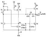
도 4를 참조하면, 본 발명의 제1 실시예에 따른 쉬프트 레지스터의 스테이지들 각각은 제1 노드(P1)와 출력라인(4i) 사이에 직렬접속되어진 캐패시터들(CP1a,CP1b)과; 제2 노드(P2)와 기저전압라인(10) 사이에 직렬접속되어진 캐패시터들(CP2a,CP2b)과; 제1 노드(P1)와 기저전압라인(10) 사이에 직렬접속되어진 캐패시터들(CP12a,CP12b)을 구비한다. 직렬 접속된 캐패시터들(CP1a,CP1b,CP2a,CP2b,CP12a,CP12b) 중 어느 하나가 단락되더라도 쉬프트 레지스터가 정상적으로 동작될 수 있도록 한다. 즉, 직렬 접속된 캐패시터들 중 어느 하나는 리던던스(Redundancy) 역할을 하게 된다. 이를 상세히 하면, 제1 노드(P1)와 출력라인(4i) 사이에 직렬접속된 캐패시터들(CP1a,CP1b) 중 어느 하나가 단락되더라도 다른 캐패시터는 하이레벨전압의 제1 클럭신호(C1)가 출력라인(4i)에 공급될 때 제1 클럭신호(C1)의 전압레벨만큼 제1 노드(P1)상의 전압을 승압시킨다. 이 캐패시터(CP1)에 의해 게이트 전압이 증가됨으로써, 제5 NMOS 트랜지스터(T5)는 제1 클럭신호(C1)를 감쇠없이 빠르게 출력라인(4i)쪽으로 전달하게 된다. 제2 노드(P2)와 기저전압라인(10) 사이에 직렬 접속된 캐패시터들(CP2a,CP2b) 중 어느 하나가 단락되더라도 다른 캐패시터는 출력노드(4i) 상의 출력전압(Vout)이 변화할 때 제2 노드(P2) 상의 전압변화를 억제함과 아울러 NMOS 트랜지스터들로부터 누설되는 누설전류에 의한 제2 노드(P2) 상의 전압변화를 억제하게 된다. 제1 노드(P1)와 기저전압라인(10) 사이에 직렬 접속된 캐패시터들(CP12a,CP12b)은 제1 노드(P1) 상의 전압 상승폭(ΔVp)을 설정하게 되며, 둘 중 어느 하나가 단락되더라도 다른 하나의 캐패시터가 제2 노드(P2) 상의 전압을 충방전함으로써 제2 노드(P2) 상의 전압 상승폭(ΔVp)을 정확하게 조정할 수 있게 된다.4, each of the stages of the shift register according to the first embodiment of the present invention includes capacitors CP1a and CP1b connected in series between the first node P1 and the
도 2에 도시된 쉬프트 레지스터의 스테이지와 대비할 때, 도 4에 도시된 스테이지는 두 배의 캐패시터가 필요하며, 각 캐패시터의 캐패시턴스는 2 배로 된다. 또한, 캐패시터들(CP1a,CP1b,CP2a,CP2b,CP12a,CP12b)이 차지하는 면적은 4배가 된다.In contrast to the stage of the shift register shown in FIG. 2, the stage shown in FIG. 4 requires twice the capacitor, and the capacitance of each capacitor is doubled. In addition, the area occupied by the capacitors CP1a, CP1b, CP2a, CP2b, CP12a, CP12b is four times larger.
본 발명에 따른 쉬프트 레지스터의 스테이지들 각각은 이전 스테이지(2i-1)의 로우라인(4i-1), 제1 노드(P1) 및 제4 노드(P4) 사이에 접속되어진 제1 NMOS 트랜지스터(T1)와; 제1 노드(P1), 제2 노드(P2) 및 기저전압라인(10) 사이에 접속되어진 제2 NMOS 트랜지스터(T2)와, 공급전압라인(8), 제3 클런신호라인(6c) 및 제2 노드(P2) 사이에 접속되어진 제3 NMOS 트랜지스터(T3)와; 제2 노드(P2), 제4 노드(P4) 및 기저전압라인(10) 사이에 접속되어진 제4 NMOS 트랜지스터(T4)와; 제1 노드(P1), 제1 클럭신호라인(6a) 및 출력라인(4i) 사이에 접속되어진 제5 NMOS 트랜지스터(T5)와; 제2 노드(P2), 출력라인(4i) 및 기저전압라인(10) 사이에 접속되어진 제6 NMOS 트랜지스터(T6)를 구비한다. 이와 같은 스테이지의 동작은 도 2에 도시된 스테이지의 동작과 실질적으로 동일하므로 상세한 설명을 생략하기로 한다.Each of the stages of the shift register according to the present invention is a first NMOS transistor T1 connected between the
직렬 접속된 캐패시터들은 TFT들의 제조공정을 이용하여 도 5 및 도 6과 같은 구조로 형성될 수 있다.Capacitors connected in series may be formed in a structure as shown in FIGS. 5 and 6 using the manufacturing process of TFTs.
도 5를 참조하면, 기판(12) 상에는 게이트메탈층(14), 제1 절연막(16), 소오스/드레인메탈층(22), 제2 절연막(18) 및 투명전극층(20)을 적층시키게 된다. 게이트메탈층(14)과 소오스/드레인메탈층(22) 사이에 하나의 캐패시터가 형성되며, 투명전극층(20)과 소오스/드레인메탈층(22) 사이에 또 다른 캐패시터가 형성된다. 여기서, 제1 및 제2 절연막(16,18) 중 어느 하나에 파티클이 혼입되어도 캐패시터가 형성될 수 있다. 아울러, 투명전극층(20)과 게이트메탈층(14) 사이에 캐패시터가 형성된다.Referring to FIG. 5, a
도 6을 참조하면, 직렬 접속된 캐패시터들은 기판(12) 상에 적층된 게이트메탈층(14), 절연막(16), 제1 및 제2 소오스/드레인메탈층(22a,22b)에 의해 형성된다. 게이트메탈층(14)과 제1 소오스/드레인메탈층(22a) 사이에 하나의 캐패시터가 형성되며, 게이트메탈층(14)과 제2 소오스/드레인메탈층(22b) 사이에 또 다른 캐패시터가 형성된다.Referring to FIG. 6, capacitors connected in series are formed by a
도 7은 본 발명의 제2 실시예에 따른 쉬프트 레지스터의 스테이지를 나타낸다.7 shows a stage of a shift register according to a second embodiment of the present invention.
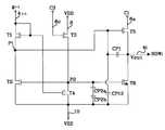
도 7을 참조하면, 본 발명에 따른 쉬프트 레지스터의 스테이지들 각각은 제1 노드(P1)와 출력라인(4i) 사이에 접속되어진 캐패시터들(CP1,CP3)과; 제2 노드(P2)와 기저전압라인(10) 사이에 직렬접속되어진 캐패시터들(CP2a,CP2b)과; 제3 노드(P3)와 기저전압라인(10) 사이에 접속되어진 캐패시터(CP12)를 구비한다. 제1 노드(P1)와 제3 노드(P3) 사이에 접속된 캐패시터(CP3)는 제3 노드(P3)를 경유하여 자신에게 병렬 접속된 캐패시터들(CP1,CP12)의 리던던스 역할을 하게 된다. 다시 말하여, 이들 캐패시터들(CP1,CP3,CP12) 중 어느 하나가 단락되더라도 쉬프트 레지스터가 오동작되지 않게 된다. 이들 캐패시터들(CP1,CP3,CP12) 중 제1 노드(P1)와 제3 노드(P3) 사이에 접속된 캐패시터(CP3)가 단락되는 경우에는 제2 노드(P2)와 기저전압라인(10) 사이에 캐패시터들(CP2a,CP2b)이 직렬 접속된 것을 제외하고 도 2에 도시된 스테이지와 동일한 회로로 구성된다. 제3 노드(P3)와 출력라인(4i) 사이에 접속된 캐패시터(CP1)가 단락된 경우, 스테이지가 제3 노드(P3)와 기저전압라인(10) 사이에 접속된 캐패시터(CP12)가 없는 것과 동일하게 동작한다. 제3 노드(P3)와 기저전압라인(10) 사이에 접속된 캐패시터(CP12)가 단락된 경우, 스테이지는 도 2에 도시된 스테이지에서 제1 노드(P1)와 출력라인(4i) 사이에 접속된 캐패시터(CP1)가 없는 것과 동일하게 동작한다. 제2 노드(P2)와 기저전압라인(10) 사이에 직렬 접속된 캐패시터들(CP2a,CP2b)과 제1 노드(P1)와 출력라인(4i) 사이에 직렬 접속된 캐패시터들(CP3,CP1)은 도 5 및 도 6과 같은 구조로 형성된다.Referring to FIG. 7, each of the stages of the shift register according to the present invention includes capacitors CP1 and CP3 connected between the first node P1 and the
한편, 제3 노드(P3)와 출력라인(4i) 사이에 접속된 캐패시터(CP1)가 단락된 경우에는 제1 노드(P1) 상의 누설전류가 증가할 수 있으므로 스테이지가 다소 불안정하게 동작할 수 있다. 또한, 제3 노드(P3)와 기저전압라인(10) 사이에 접속된 캐패시터(CP12)가 단락된 경우에는 출력라인(4i)에 나타나는 출력전압이 다소 감소할 수 있다. 이러한 경우에 있어서, 스테이지에 캐패시터들을 설치하는 목적이 소자들의 특성이 불균일할 때 발생하는 불안정성을 줄이기 위한 것이므로 TFT들이 안정적인 특성을 가질 경우에는 캐패시터들(CP1,CP12)이 단락되더라도 정상적으로 동 작한다.On the other hand, when the capacitor CP1 connected between the third node P3 and the
도 2에 도시된 쉬프트 레지스터의 스테이지와 대비할 때, 도 7에 도시된 스테이지는 캐패시터들의 총용량은 대략 1.5 배가 필요하며, 캐패시터들이 차지하는 면적은 2.2배가 된다. 그리고 도 4에 도시된 스테이지와 대비할 때, 도 7에 도시된 스테이지는 캐패시터 수가 하나 줄게 되며, 이에 따라 캐패시터들이 차지하는 면적과 필요한 캐패시턴스가 줄게 된다. In contrast to the stage of the shift register shown in FIG. 2, the stage shown in FIG. 7 requires approximately 1.5 times the total capacity of the capacitors and 2.2 times the area occupied by the capacitors. In contrast to the stage illustrated in FIG. 4, the stage illustrated in FIG. 7 reduces the number of capacitors by one, thereby reducing the area occupied by the capacitors and the required capacitance.
도 8은 본 발명의 제3 실시예에 따른 쉬프트 레지스터의 스테이지를 나타낸다.8 shows a stage of a shift register according to a third embodiment of the present invention.
도 8을 참조하면, 본 발명에 따른 쉬프트 레지스터의 스테이지들 각각은 제1 노드(P1)와 출력라인(4i) 사이에 접속되어진 캐패시터(CP1)와; 제2 노드(P2)와 기저전압라인(10) 사이에 직렬접속되어진 캐패시터들(CP2a,CP2b)과; 제1 노드(P1)와 기저전압라인(10) 사이에 접속되어진 캐패시터(CP12)를 구비한다. 이와 같은 스테이지들은 패널의 좌우측에 쉬프트 레지스터가 배치되는 경우에 이용될 수 있다. 패널의 좌우측에 쉬프트 레지스터가 배치되면, 출력라인(4i)에 종속적으로 접속된 캐패시터들(CP1,CP12)이 단락되더라도 출력라인(4i)의 반대측에 위치한 스테이지의 구동에 의해 정상적으로 구동될 수 있다. 이에 따라, 패널의 좌우측에 쉬프트 레지스터가 배치되는 경우에 제2 노드(P2)와 기저전압라인(10) 사이에 위치한 캐패시터의 단락만 방지하면 정상적으로 동작할 수 있으므로 제2 노드(P2)와 기저전압라인(10) 사이에 위치한 캐패시터들(CP2a,CP2b)만 두 개 이상으로 직렬접속시키게 된다. 이렇게 제2 노드(P2)와 기저전압라인(10) 사이에 위치한 캐패시터들(CP2a,CP2b)만 두 개 이상으로 직렬접속시킴으로써, 캐패시터의 단락을 방지할 수 있게 된다.8, each of the stages of the shift register according to the present invention includes a capacitor CP1 connected between the first node P1 and the
상술한 바와 같이, 본 발명에 따른 쉬프트 레지스터는 출력 노드와 부트스트랩 노드 사이와 직류전원과 부트스트랩 노드 사이에 접속된 캐패시터를 두 개 이상으로 직렬 접속시킴으로써 캐패시터의 단락을 방지할 수 있게 된다.As described above, the shift register according to the present invention can prevent the short circuit of the capacitor by serially connecting two or more capacitors connected between the output node and the bootstrap node and between the DC power source and the bootstrap node.
그리고, 본 발명은 제어전극과 저전위 전압원 사이에 직렬 접속된 캐패시터들(CP12a,CP12b)이 제1 노드(P1) 상의 전압 상승폭(ΔVp)을 설정하게 됨으로써, 둘 중 어느 하나가 단락되더라도 다른 하나의 캐패시터가 제2 노드(P2) 상의 전압을 충방전함으로써 제2 노드(P2) 상의 전압 상승폭(ΔVp)을 정확하게 조정할 수 있게 된다.
또한, 본 발명은 제어전극과 저전위 전압원 사이에 직렬 위치한 캐패시터들(CP2a,CP2b)만 직렬접속시킴으로써, 캐패시터의 단락을 방지할 수 있게 된다.
이상 설명한 내용을 통해 당업자라면 본 발명의 기술사상을 일탈하지 아니하는 범위에서 다양한 변경 및 수정이 가능함을 알 수 있을 것이다. 따라서, 본 발명의 기술적 범위는 명세서의 상세한 설명에 기재된 내용으로 한정되는 것이 아니라 특허 청구의 범위에 의해 정하여 져야만 할 것이다.In the present invention, the capacitors CP12a and CP12b connected in series between the control electrode and the low potential voltage source set the voltage rising width ΔVp on the first node P1, so that the other one is short-circuited. Capacitor of charge and discharge the voltage on the second node (P2) it is possible to accurately adjust the voltage rise (ΔVp) on the second node (P2).
In addition, the present invention can prevent the short circuit of the capacitor by serially connecting only the capacitors CP2a and CP2b positioned in series between the control electrode and the low potential voltage source.
Those skilled in the art will appreciate that various changes and modifications can be made without departing from the technical spirit of the present invention. Therefore, the technical scope of the present invention should not be limited to the contents described in the detailed description of the specification but should be defined by the claims.
Claims (7)
Translated fromKoreanPriority Applications (2)
| Application Number | Priority Date | Filing Date | Title |
|---|---|---|---|
| KR1019990048738AKR100685307B1 (en) | 1999-11-05 | 1999-11-05 | Shift register |
| US09/705,714US6345085B1 (en) | 1999-11-05 | 2000-11-06 | Shift register |
Applications Claiming Priority (1)
| Application Number | Priority Date | Filing Date | Title |
|---|---|---|---|
| KR1019990048738AKR100685307B1 (en) | 1999-11-05 | 1999-11-05 | Shift register |
Publications (2)
| Publication Number | Publication Date |
|---|---|
| KR20010045445A KR20010045445A (en) | 2001-06-05 |
| KR100685307B1true KR100685307B1 (en) | 2007-02-22 |
Family
ID=19618634
Family Applications (1)
| Application Number | Title | Priority Date | Filing Date |
|---|---|---|---|
| KR1019990048738AExpired - LifetimeKR100685307B1 (en) | 1999-11-05 | 1999-11-05 | Shift register |
Country Status (2)
| Country | Link |
|---|---|
| US (1) | US6345085B1 (en) |
| KR (1) | KR100685307B1 (en) |
Families Citing this family (60)
| Publication number | Priority date | Publication date | Assignee | Title |
|---|---|---|---|---|
| US7569849B2 (en)* | 2001-02-16 | 2009-08-04 | Ignis Innovation Inc. | Pixel driver circuit and pixel circuit having the pixel driver circuit |
| JP4310939B2 (en)* | 2001-06-29 | 2009-08-12 | カシオ計算機株式会社 | Shift register and electronic device |
| CA2355067A1 (en)* | 2001-08-15 | 2003-02-15 | Ignis Innovations Inc. | Metastability insensitive integrated thin film multiplexer |
| KR100415618B1 (en)* | 2001-12-26 | 2004-01-24 | 엘지.필립스 엘시디 주식회사 | Shift Register |
| GB2397710A (en)* | 2003-01-25 | 2004-07-28 | Sharp Kk | A shift register for an LCD driver, comprising reset-dominant RS flip-flops |
| CA2419704A1 (en) | 2003-02-24 | 2004-08-24 | Ignis Innovation Inc. | Method of manufacturing a pixel with organic light-emitting diode |
| JP4522057B2 (en)* | 2003-06-30 | 2010-08-11 | 三洋電機株式会社 | Display device |
| KR100987709B1 (en)* | 2003-07-01 | 2010-10-13 | 삼성전자주식회사 | LCD Display |
| CA2443206A1 (en) | 2003-09-23 | 2005-03-23 | Ignis Innovation Inc. | Amoled display backplanes - pixel driver circuits, array architecture, and external compensation |
| KR101012972B1 (en)* | 2003-12-30 | 2011-02-10 | 엘지디스플레이 주식회사 | Active matrix display |
| KR101023726B1 (en)* | 2004-03-31 | 2011-03-25 | 엘지디스플레이 주식회사 | Shift register |
| KR101143803B1 (en)* | 2004-03-31 | 2012-05-11 | 엘지디스플레이 주식회사 | Shift register and method for driving the same |
| US7289594B2 (en)* | 2004-03-31 | 2007-10-30 | Lg.Philips Lcd Co., Ltd. | Shift registrer and driving method thereof |
| JP4732709B2 (en)* | 2004-05-20 | 2011-07-27 | 株式会社半導体エネルギー研究所 | Shift register and electronic device using the same |
| KR101030528B1 (en)* | 2004-05-27 | 2011-04-26 | 엘지디스플레이 주식회사 | Shift register and liquid crystal display using the same |
| CA2472671A1 (en) | 2004-06-29 | 2005-12-29 | Ignis Innovation Inc. | Voltage-programming scheme for current-driven amoled displays |
| CN100353460C (en)* | 2004-08-16 | 2007-12-05 | 友达光电股份有限公司 | Shift register and display panel using the shift register |
| CA2490858A1 (en) | 2004-12-07 | 2006-06-07 | Ignis Innovation Inc. | Driving method for compensated voltage-programming of amoled displays |
| CA2495726A1 (en) | 2005-01-28 | 2006-07-28 | Ignis Innovation Inc. | Locally referenced voltage programmed pixel for amoled displays |
| TW200746022A (en) | 2006-04-19 | 2007-12-16 | Ignis Innovation Inc | Stable driving scheme for active matrix displays |
| TWI366814B (en)* | 2006-07-12 | 2012-06-21 | Wintek Corp | Shift register |
| CN101908381B (en)* | 2009-06-04 | 2013-02-06 | 胜华科技股份有限公司 | Shift Register |
| US8497828B2 (en) | 2009-11-12 | 2013-07-30 | Ignis Innovation Inc. | Sharing switch TFTS in pixel circuits |
| US9606607B2 (en) | 2011-05-17 | 2017-03-28 | Ignis Innovation Inc. | Systems and methods for display systems with dynamic power control |
| CN109272933A (en) | 2011-05-17 | 2019-01-25 | 伊格尼斯创新公司 | The method for operating display |
| US8901579B2 (en) | 2011-08-03 | 2014-12-02 | Ignis Innovation Inc. | Organic light emitting diode and method of manufacturing |
| US9070775B2 (en) | 2011-08-03 | 2015-06-30 | Ignis Innovations Inc. | Thin film transistor |
| US9385169B2 (en) | 2011-11-29 | 2016-07-05 | Ignis Innovation Inc. | Multi-functional active matrix organic light-emitting diode display |
| US10089924B2 (en) | 2011-11-29 | 2018-10-02 | Ignis Innovation Inc. | Structural and low-frequency non-uniformity compensation |
| CN102629463B (en)* | 2012-03-29 | 2013-10-09 | 京东方科技集团股份有限公司 | Shift register unit, shift register circuit, array substrate and display device |
| KR101975533B1 (en)* | 2012-06-29 | 2019-05-08 | 삼성디스플레이 주식회사 | Driving circuit, flat panel display device having the same and method for repairing the driving circuit |
| US9299452B2 (en)* | 2012-08-09 | 2016-03-29 | Innocom Technology (Shenzhen) Co., Ltd. | Shift registers, display panels, display devices, and electronic devices |
| TWI505245B (en)* | 2012-10-12 | 2015-10-21 | Au Optronics Corp | Shift register |
| JP2014142457A (en)* | 2013-01-23 | 2014-08-07 | Japan Display Inc | Display device |
| US9721505B2 (en) | 2013-03-08 | 2017-08-01 | Ignis Innovation Inc. | Pixel circuits for AMOLED displays |
| US9952698B2 (en) | 2013-03-15 | 2018-04-24 | Ignis Innovation Inc. | Dynamic adjustment of touch resolutions on an AMOLED display |
| RU2522306C1 (en)* | 2013-04-05 | 2014-07-10 | Федеральное государственное бюджетное учреждение науки Институт физики полупроводников им. А.В. Ржанова Сибирского отделения Российской академии наук (ИФП СО РАН) | Shift register |
| CN103258495B (en) | 2013-05-07 | 2015-08-05 | 京东方科技集团股份有限公司 | Shifting deposit unit, shift register and display device |
| US9054696B2 (en)* | 2013-10-12 | 2015-06-09 | Shenzhen China Star Optoelectronics Technology Co., Ltd. | Gate driving circuit, and array substrate and display panel using the same |
| US9502653B2 (en) | 2013-12-25 | 2016-11-22 | Ignis Innovation Inc. | Electrode contacts |
| US10997901B2 (en) | 2014-02-28 | 2021-05-04 | Ignis Innovation Inc. | Display system |
| US10176752B2 (en) | 2014-03-24 | 2019-01-08 | Ignis Innovation Inc. | Integrated gate driver |
| CN104036738B (en)* | 2014-03-27 | 2016-06-01 | 京东方科技集团股份有限公司 | A kind of shift register cell, gate driver circuit and display unit |
| CN104318904B (en)* | 2014-11-20 | 2017-08-01 | 京东方科技集团股份有限公司 | Shift register unit and driving method thereof, shift register, display device |
| CA2872563A1 (en) | 2014-11-28 | 2016-05-28 | Ignis Innovation Inc. | High pixel density array architecture |
| KR102283461B1 (en)* | 2014-12-22 | 2021-07-29 | 엘지디스플레이 주식회사 | Liquid crystal display device |
| CN104851383B (en) | 2015-06-01 | 2017-08-11 | 京东方科技集团股份有限公司 | Shift register, gate driving circuit and display device |
| US10657895B2 (en) | 2015-07-24 | 2020-05-19 | Ignis Innovation Inc. | Pixels and reference circuits and timing techniques |
| CA2898282A1 (en) | 2015-07-24 | 2017-01-24 | Ignis Innovation Inc. | Hybrid calibration of current sources for current biased voltage progra mmed (cbvp) displays |
| US10373554B2 (en) | 2015-07-24 | 2019-08-06 | Ignis Innovation Inc. | Pixels and reference circuits and timing techniques |
| KR102426106B1 (en)* | 2015-07-28 | 2022-07-29 | 삼성디스플레이 주식회사 | Stage circuit and scan driver using the same |
| CA2909813A1 (en) | 2015-10-26 | 2017-04-26 | Ignis Innovation Inc | High ppi pattern orientation |
| CN105427799B (en)* | 2016-01-05 | 2018-03-06 | 京东方科技集团股份有限公司 | Shifting deposit unit, shift register, gate driving circuit and display device |
| US10586491B2 (en) | 2016-12-06 | 2020-03-10 | Ignis Innovation Inc. | Pixel circuits for mitigation of hysteresis |
| US10714018B2 (en) | 2017-05-17 | 2020-07-14 | Ignis Innovation Inc. | System and method for loading image correction data for displays |
| CN107154244B (en)* | 2017-07-10 | 2019-08-02 | 深圳市华星光电技术有限公司 | GOA circuit and liquid crystal display device |
| US11025899B2 (en) | 2017-08-11 | 2021-06-01 | Ignis Innovation Inc. | Optical correction systems and methods for correcting non-uniformity of emissive display devices |
| US10971078B2 (en) | 2018-02-12 | 2021-04-06 | Ignis Innovation Inc. | Pixel measurement through data line |
| CN109064993B (en) | 2018-11-06 | 2020-01-21 | 合肥京东方光电科技有限公司 | Shift register and driving method thereof, grid driving circuit and display device |
| CN111508417A (en)* | 2020-05-06 | 2020-08-07 | Tcl华星光电技术有限公司 | GOA circuit |
Citations (4)
| Publication number | Priority date | Publication date | Assignee | Title |
|---|---|---|---|---|
| JPH06123896A (en)* | 1992-10-13 | 1994-05-06 | Toshiba Corp | Liquid crystal display |
| JPH1031202A (en)* | 1996-04-12 | 1998-02-03 | Thomson Multimedia Sa | Selection line driver for display matrix having toggling back plane |
| KR19980702957A (en)* | 1996-01-11 | 1998-09-05 | 루엘랑브리지뜨 | Improvements for Shift Registers Using MI I Transistors with Identical Polarity |
| KR19990029504A (en)* | 1997-09-03 | 1999-04-26 | 아베 아키라 | Shift register device and display device |
Family Cites Families (1)
| Publication number | Priority date | Publication date | Assignee | Title |
|---|---|---|---|---|
| JPH05333808A (en)* | 1992-05-29 | 1993-12-17 | Sharp Corp | Display driving circuit |
- 1999
- 1999-11-05KRKR1019990048738Apatent/KR100685307B1/ennot_activeExpired - Lifetime
- 2000
- 2000-11-06USUS09/705,714patent/US6345085B1/ennot_activeExpired - Lifetime
Patent Citations (4)
| Publication number | Priority date | Publication date | Assignee | Title |
|---|---|---|---|---|
| JPH06123896A (en)* | 1992-10-13 | 1994-05-06 | Toshiba Corp | Liquid crystal display |
| KR19980702957A (en)* | 1996-01-11 | 1998-09-05 | 루엘랑브리지뜨 | Improvements for Shift Registers Using MI I Transistors with Identical Polarity |
| JPH1031202A (en)* | 1996-04-12 | 1998-02-03 | Thomson Multimedia Sa | Selection line driver for display matrix having toggling back plane |
| KR19990029504A (en)* | 1997-09-03 | 1999-04-26 | 아베 아키라 | Shift register device and display device |
Also Published As
| Publication number | Publication date |
|---|---|
| KR20010045445A (en) | 2001-06-05 |
| US6345085B1 (en) | 2002-02-05 |
Similar Documents
| Publication | Publication Date | Title |
|---|---|---|
| KR100685307B1 (en) | Shift register | |
| US11361728B2 (en) | Gate driving circuit and display apparatus having the same | |
| KR100281336B1 (en) | Shift register circuit | |
| KR100698239B1 (en) | Shift register circuit | |
| KR100438525B1 (en) | Shift Register Circuit | |
| CN100401175C (en) | Liquid crystal display device | |
| CN110060645B (en) | Shifting register and driving method thereof, grid driving circuit and display device | |
| JP4439761B2 (en) | Liquid crystal display device, electronic equipment | |
| US6232948B1 (en) | Liquid crystal display driving circuit with low power consumption and precise voltage output | |
| US8102340B2 (en) | Liquid crystal display device | |
| KR100405026B1 (en) | Liquid Crystal Display | |
| EP1783777B1 (en) | Shift register circuit | |
| US20090041177A1 (en) | Shift register arrays | |
| WO2024113218A1 (en) | Driving circuit, display apparatus, and method of operating driving circuit | |
| WO2024103333A1 (en) | Display substrate and display apparatus | |
| CN101727800B (en) | Semiconductor gate driving circuit and driving method thereof | |
| WO2024187374A9 (en) | Array substrate and display apparatus | |
| US12046212B2 (en) | GOA circuit and display panel | |
| US20060125743A1 (en) | LCD panel driving device and conductive pattern on LCD panel therefore | |
| KR100776500B1 (en) | Shift register circuit | |
| JP3040885B2 (en) | Voltage booster circuit | |
| JP6691185B2 (en) | Semiconductor device | |
| US12148358B2 (en) | Scan circuit and display apparatus | |
| JP2020035509A (en) | Semiconductor device | |
| CN118711544A (en) | Gate drive circuit and display device |
Legal Events
| Date | Code | Title | Description |
|---|---|---|---|
| PA0109 | Patent application | Patent event code:PA01091R01D Comment text:Patent Application Patent event date:19991105 | |
| PG1501 | Laying open of application | ||
| A201 | Request for examination | ||
| PA0201 | Request for examination | Patent event code:PA02012R01D Patent event date:20041105 Comment text:Request for Examination of Application Patent event code:PA02011R01I Patent event date:19991105 Comment text:Patent Application | |
| E902 | Notification of reason for refusal | ||
| PE0902 | Notice of grounds for rejection | Comment text:Notification of reason for refusal Patent event date:20060821 Patent event code:PE09021S01D | |
| E701 | Decision to grant or registration of patent right | ||
| PE0701 | Decision of registration | Patent event code:PE07011S01D Comment text:Decision to Grant Registration Patent event date:20070117 | |
| GRNT | Written decision to grant | ||
| PR0701 | Registration of establishment | Comment text:Registration of Establishment Patent event date:20070214 Patent event code:PR07011E01D | |
| PR1002 | Payment of registration fee | Payment date:20070215 End annual number:3 Start annual number:1 | |
| PG1601 | Publication of registration | ||
| PR1001 | Payment of annual fee | Payment date:20091218 Start annual number:4 End annual number:4 | |
| PR1001 | Payment of annual fee | Payment date:20101228 Start annual number:5 End annual number:5 | |
| PR1001 | Payment of annual fee | Payment date:20111221 Start annual number:6 End annual number:6 | |
| FPAY | Annual fee payment | Payment date:20121228 Year of fee payment:7 | |
| PR1001 | Payment of annual fee | Payment date:20121228 Start annual number:7 End annual number:7 | |
| FPAY | Annual fee payment | Payment date:20131227 Year of fee payment:8 | |
| PR1001 | Payment of annual fee | Payment date:20131227 Start annual number:8 End annual number:8 | |
| FPAY | Annual fee payment | Payment date:20150127 Year of fee payment:9 | |
| PR1001 | Payment of annual fee | Payment date:20150127 Start annual number:9 End annual number:9 | |
| FPAY | Annual fee payment | Payment date:20160128 Year of fee payment:10 | |
| PR1001 | Payment of annual fee | Payment date:20160128 Start annual number:10 End annual number:10 | |
| FPAY | Annual fee payment | Payment date:20170116 Year of fee payment:11 | |
| PR1001 | Payment of annual fee | Payment date:20170116 Start annual number:11 End annual number:11 | |
| FPAY | Annual fee payment | Payment date:20190114 Year of fee payment:13 | |
| PR1001 | Payment of annual fee | Payment date:20190114 Start annual number:13 End annual number:13 | |
| PC1801 | Expiration of term | Termination date:20200505 Termination category:Expiration of duration |