KR100684907B1 - Multi-Chip Package Reduces Peak Current During Power-Up - Google Patents
Multi-Chip Package Reduces Peak Current During Power-UpDownload PDFInfo
- Publication number
- KR100684907B1 KR100684907B1KR1020060002297AKR20060002297AKR100684907B1KR 100684907 B1KR100684907 B1KR 100684907B1KR 1020060002297 AKR1020060002297 AKR 1020060002297AKR 20060002297 AKR20060002297 AKR 20060002297AKR 100684907 B1KR100684907 B1KR 100684907B1
- Authority
- KR
- South Korea
- Prior art keywords
- power
- chip package
- chip
- memory
- level detector
- Prior art date
- Legal status (The legal status is an assumption and is not a legal conclusion. Google has not performed a legal analysis and makes no representation as to the accuracy of the status listed.)
- Expired - Fee Related
Links
Images


Classifications
- A—HUMAN NECESSITIES
- A61—MEDICAL OR VETERINARY SCIENCE; HYGIENE
- A61F—FILTERS IMPLANTABLE INTO BLOOD VESSELS; PROSTHESES; DEVICES PROVIDING PATENCY TO, OR PREVENTING COLLAPSING OF, TUBULAR STRUCTURES OF THE BODY, e.g. STENTS; ORTHOPAEDIC, NURSING OR CONTRACEPTIVE DEVICES; FOMENTATION; TREATMENT OR PROTECTION OF EYES OR EARS; BANDAGES, DRESSINGS OR ABSORBENT PADS; FIRST-AID KITS
- A61F9/00—Methods or devices for treatment of the eyes; Devices for putting in contact-lenses; Devices to correct squinting; Apparatus to guide the blind; Protective devices for the eyes, carried on the body or in the hand
- A61F9/02—Goggles
- A61F9/029—Additional functions or features, e.g. protection for other parts of the face such as ears, nose or mouth; Screen wipers or cleaning devices
- G—PHYSICS
- G11—INFORMATION STORAGE
- G11C—STATIC STORES
- G11C5/00—Details of stores covered by group G11C11/00
- G11C5/14—Power supply arrangements, e.g. power down, chip selection or deselection, layout of wirings or power grids, or multiple supply levels
- G11C5/143—Detection of memory cassette insertion or removal; Continuity checks of supply or ground lines; Detection of supply variations, interruptions or levels ; Switching between alternative supplies
- A—HUMAN NECESSITIES
- A41—WEARING APPAREL
- A41D—OUTERWEAR; PROTECTIVE GARMENTS; ACCESSORIES
- A41D13/00—Professional, industrial or sporting protective garments, e.g. surgeons' gowns or garments protecting against blows or punches
- A41D13/05—Professional, industrial or sporting protective garments, e.g. surgeons' gowns or garments protecting against blows or punches protecting only a particular body part
- A—HUMAN NECESSITIES
- A61—MEDICAL OR VETERINARY SCIENCE; HYGIENE
- A61F—FILTERS IMPLANTABLE INTO BLOOD VESSELS; PROSTHESES; DEVICES PROVIDING PATENCY TO, OR PREVENTING COLLAPSING OF, TUBULAR STRUCTURES OF THE BODY, e.g. STENTS; ORTHOPAEDIC, NURSING OR CONTRACEPTIVE DEVICES; FOMENTATION; TREATMENT OR PROTECTION OF EYES OR EARS; BANDAGES, DRESSINGS OR ABSORBENT PADS; FIRST-AID KITS
- A61F9/00—Methods or devices for treatment of the eyes; Devices for putting in contact-lenses; Devices to correct squinting; Apparatus to guide the blind; Protective devices for the eyes, carried on the body or in the hand
- A61F9/02—Goggles
- A61F9/027—Straps; Buckles; Attachment of headbands
- G—PHYSICS
- G02—OPTICS
- G02C—SPECTACLES; SUNGLASSES OR GOGGLES INSOFAR AS THEY HAVE THE SAME FEATURES AS SPECTACLES; CONTACT LENSES
- G02C11/00—Non-optical adjuncts; Attachment thereof
- G02C11/04—Illuminating means
- G—PHYSICS
- G02—OPTICS
- G02C—SPECTACLES; SUNGLASSES OR GOGGLES INSOFAR AS THEY HAVE THE SAME FEATURES AS SPECTACLES; CONTACT LENSES
- G02C11/00—Non-optical adjuncts; Attachment thereof
- G02C11/10—Electronic devices other than hearing aids
- G—PHYSICS
- G11—INFORMATION STORAGE
- G11C—STATIC STORES
- G11C5/00—Details of stores covered by group G11C11/00
- G11C5/02—Disposition of storage elements, e.g. in the form of a matrix array
- G11C5/04—Supports for storage elements, e.g. memory modules; Mounting or fixing of storage elements on such supports
Landscapes
- Health & Medical Sciences (AREA)
- Engineering & Computer Science (AREA)
- Physics & Mathematics (AREA)
- General Health & Medical Sciences (AREA)
- Ophthalmology & Optometry (AREA)
- Biomedical Technology (AREA)
- Vascular Medicine (AREA)
- General Physics & Mathematics (AREA)
- Veterinary Medicine (AREA)
- Optics & Photonics (AREA)
- Power Engineering (AREA)
- Heart & Thoracic Surgery (AREA)
- Otolaryngology (AREA)
- Life Sciences & Earth Sciences (AREA)
- Animal Behavior & Ethology (AREA)
- Public Health (AREA)
- Acoustics & Sound (AREA)
- Physical Education & Sports Medicine (AREA)
- Textile Engineering (AREA)
- Read Only Memory (AREA)
- Static Random-Access Memory (AREA)
Abstract
Translated fromKoreanDescription
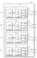
Translated fromKorean도 1은 본 발명에 따른 멀티 칩 패키지를 보여주는 블록도이다.1 is a block diagram illustrating a multi-chip package according to the present invention.
도 2는 도 1에 도시된 멀티 칩 패키지의 본딩 옵션에 따른 본딩 옵션 신호의 전압 레벨을 예시적으로 보여주는 도표이다.FIG. 2 is a diagram illustrating a voltage level of a bonding option signal according to the bonding option of the multi-chip package illustrated in FIG. 1.
도 3은 도 1에 도시된 멀티 칩 패키지의 초기화 신호의 파형 및 전류 소모를 보여준다.FIG. 3 shows waveforms and current consumption of the initialization signal of the multi-chip package shown in FIG. 1.
*도면의 주요부분에 대한 부호의 설명** Explanation of symbols for main parts of drawings *
100; 멀티 칩 패키지100; Multi-chip package
110, 120, 130, 140; 메모리 칩110, 120, 130, 140; Memory chip
111, 121, 131, 141; 내부 회로111, 121, 131, 141; Internal circuit
112, 122, 132, 142; 파워 레벨 검출기112, 122, 132, 142; Power level detector
본 발명은 멀티 칩 패키지에 관한 것으로서, 더욱 상세하게는 복수의 메모리 칩을 포함한 멀티 칩 패키지에 관한 것이다.The present invention relates to a multi-chip package, and more particularly to a multi-chip package including a plurality of memory chips.
멀티 칩 패키지는 복수의 반도체 메모리 칩을 포함한다. 반도체 메모리 칩은 데이터를 저장해 두고 필요할 때 꺼내어 읽어볼 수 있는 기억장치이다. 반도체 메모리 칩은 크게 RAM(Random Access Memory)과 ROM(Read Only Memory)으로 나눌 수 있다. ROM은 전원이 끊어지더라도 저장된 데이터가 소멸하지 않는 불휘발성 메모리(nonvolatile memory)이다. ROM에는 PROM(Programmable ROM), EPROM(Erasable PROM), EEPROM(Electrically EPROM), 플래시 메모리(Flash Memory Device) 등이 있다. RAM은 전원이 끊어지면 저장된 데이터가 소멸하는 소위 휘발성 메모리(volatile memory)이다. RAM에는 Dynamic RAM(DRAM)과 Static RAM(SRAM) 등이 있다.The multi-chip package includes a plurality of semiconductor memory chips. A semiconductor memory chip is a memory device that stores data and can be read out when needed. Semiconductor memory chips can be roughly divided into random access memory (RAM) and read only memory (ROM). ROM is nonvolatile memory that does not lose its stored data even when its power supply is interrupted. The ROM includes PROM (Programmable ROM), EPROM (Erasable PROM), EEPROM (Electrically EPROM), Flash Memory (Flash Memory Device) and the like. RAM is a so-called volatile memory that loses its stored data when the power is turned off. RAM includes Dynamic RAM (DRAM) and Static RAM (SRAM).
멀티 칩 패키지에서 각각의 메모리 칩은 파워 업(power_up) 시에 전원 전압의 레벨을 감지하여 래치 등을 초기화하는 파워 레벨 검출기(Power Level Detector; PLD)를 포함한다. 각각의 메모리 칩의 파워 레벨 검출기는 전원 전압이 일정한 레벨에 도달할 때, 각각의 내부 회로의 래치 등을 초기화한다.In the multi-chip package, each memory chip includes a power level detector (PLD) that detects a level of a power supply voltage and initializes a latch or the like upon power-up. The power level detector of each memory chip initializes latches and the like of each internal circuit when the power supply voltage reaches a constant level.
각각의 파워 레벨 검출기가 동시에 래치 등을 초기화하기 때문에, 초기화 신호의 발생 시에 전류 소모가 증가한다. 예를 들면, 멀티 칩 패키지가 4개의 메모리 칩을 포함한다고 가정하자. 이때 멀티 칩 패키지는 각각의 메모리 칩에서 초기화 신호가 발생할 때 4배의 전류를 한꺼번에 소비하게 된다. 따라서 멀티 칩 패키지는 싱글 칩 패키지에 비해 4배의 피크 전류가 발생한다. 파워 업 시에 동시에 발생하는 피크 전류는 메모리 칩의 오동작을 야기할 수 있다.Since each power level detector initializes a latch or the like at the same time, current consumption increases when the initialization signal is generated. For example, suppose a multi-chip package contains four memory chips. In this case, the multi-chip package consumes four times the current at the same time when an initialization signal occurs in each memory chip. As a result, multi-chip packages generate four times the peak current than single-chip packages. Peak currents occurring simultaneously at power-up may cause a malfunction of the memory chip.
본 발명은 상술한 문제점을 해결하기 위하여 제안된 것으로, 본 발명의 목적은 파워 업 시에 초기화 신호의 인가에 따른 피크 전류를 줄일 수 있는 멀티 칩 패키지를 제공하는 데 있다.The present invention has been proposed to solve the above problems, and an object of the present invention is to provide a multi-chip package that can reduce the peak current due to the application of the initialization signal at power-up.
본 발명은 복수의 메모리 칩을 포함하는 멀티 칩 패키지에 관한 것이다. 본 발명에 따른 멀티 칩 패키지에서, 각각의 메모리 칩은 내부 회로; 및 파워 업 시에 전원 전압의 레벨을 감지하여 상기 내부 회로를 초기화하는 파워 레벨 검출기를 포함하며, 각각의 파워 레벨 검출기는 각각의 내부 회로의 초기화 시점을 달리한다.The present invention relates to a multi-chip package including a plurality of memory chips. In the multi-chip package according to the present invention, each memory chip comprises an internal circuit; And a power level detector for initializing the internal circuit by sensing a level of a power supply voltage at power up, wherein each power level detector differs in initializing time of each internal circuit.
실시예로서, 상기 각각의 파워 레벨 검출기는 지연 소자를 사용하여 상기 초기화 시점을 달리한다. 상기 각각의 파워 레벨 검출기는 상기 각각의 내부 회로의 초기화 전압 레벨을 달리한다.As an embodiment, each power level detector uses a delay element to vary the initialization time point. The respective power level detectors vary the initialization voltage levels of the respective internal circuits.
다른 실시예로서, 상기 각각의 메모리 칩은 복수의 본딩 패드를 구비한다. 상기 복수의 본딩 패드는 전원 핀 또는 접지 핀에 연결된다. 상기 각각의 파워 레벨 검출기는 본딩 옵션을 통해 상기 초기화 시점을 달리한다.In another embodiment, each memory chip has a plurality of bonding pads. The plurality of bonding pads are connected to a power pin or a ground pin. Each power level detector differs in its initialization time through a bonding option.
또 다른 실시예로서, 상기 복수의 메모리 칩은 낸드 플래시 메모리 칩이다.In another embodiment, the plurality of memory chips are NAND flash memory chips.
이하, 본 발명이 속하는 기술분야에서 통상의 지식을 가진 자가 본 발명의 기술적 사상을 용이하게 실시할 수 있을 정도로 상세히 설명하기 위하여, 본 발명의 실시예를 첨부된 도면을 참조하여 설명한다.DETAILED DESCRIPTION Hereinafter, exemplary embodiments of the present invention will be described with reference to the accompanying drawings so that those skilled in the art may easily implement the technical idea of the present invention.
도 1은 본 발명에 따른 멀티 칩 패키지(100)를 보여주는 블록도이다. 멀티 칩 패키지(100)는 복수의 메모리 칩(110~140)을 포함한다. 도 1에서는 4개의 메모 리 칩이 도시되어 있으나, 이보다 더 많은 수의 메모리 칩이 멀티 칩 패키지(100)에 포함될 수 있다. 또한, 도 1에서는 4개의 메모리 칩이 하나의 평면에 배열되어 있으나, 4개의 메모리 칩이 층을 이루며 배열될 수도 있다.1 is a block diagram illustrating a
도 1을 참조하면, 제 1 내지 제 4 메모리 칩(110~140)은 동일한 구성 및 동작 원리를 갖는다. 따라서 이하에서는 제 1 메모리 칩(110)의 구성 및 동작이 설명된다. 제 1 메모리 칩(110)은 내부 회로(111), 파워 레벨 검출기(112), 전원 패드(10), 제 1 본딩 패드(11), 그리고 제 2 본딩 패드(12)를 포함한다.Referring to FIG. 1, the first to
내부 회로(111)는 셀 어레이(도시되지 않음)에 데이터를 저장하거나 셀 어레이에 저장된 데이터를 읽어내기 위한 회로를 포함한다. 내부 회로(111)는 데이터 쓰기 및 읽기 동작을 수행하기 위해 레지스터, 래치, 플립플롭 등(이하, 레지스터 등이라 함)을 포함한다. 여기에서, 레지스터 등은 셀 어레이에 쓸 데이터나 셀 어레로부터 읽은 데이터를 일시적으로 저장한다. 레지스터 등이 이러한 동작을 수행하기 위해서는 파워 업(power-up) 시에 초기화되어야 한다.The
파워 레벨 검출기(112)는 파워 업 시에 전원 패드(10)를 통해 전원 전압(VDD)을 입력받는다. 전원 전압(VDD)은 일정한 시간을 두고 상승한다. 파워 레벨 검출기(112)는 전원 전압(VDD)의 레벨을 감지하여, 내부 회로(111)의 레지스터 등을 초기화하기 위한 초기화 신호(INIT1)를 제공한다.The
또한, 파워 레벨 검출기(112)는 제 1 및 제 2 본딩 패드(11, 12)를 통해 각각 제 1 및 제 2 본딩 옵션 신호(Bonding Option signal; BOP1, BOP2)를 입력받는다. 파워 레벨 검출기(112)는 제 1 및 제 2 본딩 옵션 신호(BOP1, BOP2)를 디코딩 하여, 초기화 신호(INIT1)의 발생 시점을 결정한다.In addition, the
예를 들면, 파워 레벨 검출기(112)는 지연 소자를 사용하여 초기화 신호(INIT1)의 발생 시점을 조절한다. 도 1에서 제 1 및 제 2 본딩 패드(11, 12)는 모두 접지 핀에 연결되어 있다. 따라서 제 1 및 제 2 본딩 옵션 신호(BOP1, BOP2)는 모두 로우 레벨 또는 접지 레벨을 갖는다.For example, the
이와 마찬가지로, 제 2 메모리 칩(120)에서 제 1 및 제 2 본딩 패드(21, 22)는 각각 접지 핀 및 전원 핀에 연결되어 있다. 따라서 제 2 메모리 칩(120)의 제 1 본딩 옵션 신호(BOP1)는 로우 레벨을 갖고, 제 2 본딩 옵션 신호(BOP2)는 하이 레벨을 갖는다. 제 3 메모리 칩(130)에서 제 1 및 제 2 본딩 패드(31, 32)는 각각 전원 핀 및 접지 핀에 연결되어 있다. 따라서 제 3 메모리 칩(130)의 제 1 본딩 옵션 신호(BOP1)는 하이 레벨을 갖고, 제 2 본딩 옵션 신호(BOP2)는 로우 레벨을 갖는다. 그리고 제 4 메모리 칩(140)에서 제 1 및 제 2 본딩 패드(41, 42)는 모두 전원 핀에 연결되어 있다. 따라서 제 4 메모리 칩(140)의 제 1 및 제 2 본딩 옵션 신호(BOP1, BOP2)는 모두 하이 레벨을 갖는다.Similarly, in the
도 2는 도 1에 도시된 멀티 칩 패키지(100)의 본딩 옵션에 따른 본딩 옵션 신호의 전압 레벨을 예시적으로 보여주는 도표이다. 도 1 및 도 2를 참조하면, 제 1 메모리 칩(110)은 접지 레벨(GND)의 제 1 및 제 2 본딩 옵션 신호(BOP1, BOP2)에 응답하여 1V의 초기화 전압(Vinit_1)을 발생한다. 제 2 메모리 칩(120)은 접지 레벨(GND)의 제 1 본딩 옵션 신호(BOP1) 및 전원 레벨(VDD)의 제 2 본딩 옵션 신호(BOP2)에 응답하여 1.2V의 초기화 전압(Vinit_2)을 발생한다. 제 3 메모리 칩(130) 은 전원 레벨(VDD)의 제 1 본딩 옵션 신호(BOP1) 및 접지 레벨(GND)의 제 2 본딩 옵션 신호(BOP2)에 응답하여 1.4V의 초기화 전압(Vinit_3)을 발생한다. 제 4 메모리 칩(140)은 전원 레벨(VDD)의 제 1 및 제 2 본딩 옵션 신호(BOP1, BOP2)에 응답하여 1.6V의 초기화 전압(Vinit_4)을 발생한다.2 is a diagram illustrating a voltage level of a bonding option signal according to the bonding option of the
도 3은 도 1에 도시된 멀티 칩 패키지(100)의 초기화 신호(INIT1~INIT4) 파형 및 전류 소모를 보여준다. 도 3(a)는 제 1 메모리 칩(110)의 초기화 신호(INIT1)를 보여주고, 도 3(b)는 제 2 메모리 칩(120)의 초기화 신호(INIT2)를 보여주고, 도 3(c)는 제 3 메모리 칩(130)의 초기화 신호(INIT3)를 보여주고, 도 3(d)는 제 4 메모리 칩(140)의 초기화 신호(INIT4)를 보여준다. 그리고 도 3(e)는 초기화 신호(INIT1~INIT4)의 인가에 따른 멀티 칩 패키지(100)의 전류 소모를 보여준다.FIG. 3 shows waveforms and current consumption of the initialization signals INIT1 to INIT4 of the
도 3(a)를 참조하면, 전원 전압(VDD)는 파워 업 시에 t0에서 상승하기 시작한다. 제 1 초기화 신호(INIT1)는 t1에서 전원 전압(VDD)의 제 1 상승 레벨(1V)로 상승한다. 제 1 초기화 신호(INIT1)는 t1에서 t5까지 전원 전압(VDD)과 함께 상승한다. 제 1 초기화 신호(INIT1)는 t5에서 접지 레벨로 하강한다.Referring to FIG. 3A, the power supply voltage VDD starts to rise at t0 at power up. The first initialization signal INIT1 rises to the first rising level 1V of the power supply voltage VDD at t1. The first initialization signal INIT1 rises with the power supply voltage VDD from t1 to t5. The first initialization signal INIT1 falls to the ground level at t5.
도 3(b)를 참조하면, 제 2 초기화 신호(INIT2)는 t2에서 전원 전압(VDD)의 제 2 상승 레벨(1.2V)로 상승한다. 제 2 초기화 신호(INIT2)는 t2에서 t6까지 전원 전압(VDD)과 함께 상승한다. 제 2 초기화 신호(INIT2)는 t6에서 접지 레벨로 하강한다. 도 3(c)를 참조하면, 제 3 초기화 신호(INIT3)는 t3에서 전원 전압(VDD)의 제 3 상승 레벨(1.4V)로 상승한다. 제 3 초기화 신호(INIT3)는 t3에서 t7까지 전원 전압(VDD)과 함께 상승한다. 제 3 초기화 신호(INIT3)는 t7에서 접지 레벨로 하강한다. 도 3(d)를 참조하면, 제 4 초기화 신호(INIT4)는 t4에서 전원 전압(VDD)의 제 4 상승 레벨(1.6V)로 상승한다. 제 4 초기화 신호(INIT4)는 t4에서 t8까지 전원 전압(VDD)과 함께 상승한다. 제 4 초기화 신호(INIT4)는 t8에서 접지 레벨로 하강한다.Referring to FIG. 3B, the second initialization signal INIT2 rises to the second rising level 1.2V of the power supply voltage VDD at t2. The second initialization signal INIT2 rises with the power supply voltage VDD from t2 to t6. The second initialization signal INIT2 falls to the ground level at t6. Referring to FIG. 3C, the third initialization signal INIT3 rises to a third rising level 1.4V of the power supply voltage VDD at t3. The third initialization signal INIT3 rises with the power supply voltage VDD from t3 to t7. The third initialization signal INIT3 falls to the ground level at t7. Referring to FIG. 3D, the fourth initialization signal INIT4 rises to the fourth rising level 1.6V of the power supply voltage VDD at t4. The fourth initialization signal INIT4 rises with the power supply voltage VDD from t4 to t8. The fourth initialization signal INIT4 falls to the ground level at t8.
도 3(e)를 참조하면, 제 1 내지 제 4 초기화 신호(INIT1~INIT4)의 발생 시에 멀티 칩 패키지(100)에서 발생하는 전류 소모를 보여준다. 멀티 칩 패키지(100)의 전류 소모는 제 1 내지 제 4 초기화 신호(INIT1~INIT4)의 발생 시점에 각각 발생한다.Referring to FIG. 3E, current consumption generated in the
본 발명에 따른 멀티 칩 패키지(100)는 도 3(e)에서 보는 바와 같이, 초기화 신호의 발생 시점을 달리하며, 이에 따라 소모 전류가 서로 다른 시점에서 발생된다. 본 발명에 의하면, 소모 전류의 발생 시점이 다르기 때문에 파워 업 시에 피크 전류를 줄일 수 있다. 따라서 본 발명은 파워 업 시에 피크 전류로 인한 메모리 칩의 오동작을 막을 수 있다. 본 발명은 복수의 낸드 플래시 메모리 칩을 포함한 멀티 칩 패키지 등에 다양하게 적용될 수 있다.As shown in FIG. 3E, the
한편, 본 발명의 상세한 설명에서는 구체적인 실시예에 관하여 설명하였으나, 본 발명의 범위에서 벗어나지 않는 한도 내에서 여러 가지 변형이 가능함은 물론이다. 그러므로 본 발명의 범위는 상술한 실시예에 국한되어 정해져서는 안되며 후술하는 특허청구범위 뿐만 아니라 이 발명의 특허청구범위와 균등한 것들에 의해 정해져야 한다.On the other hand, in the detailed description of the present invention has been described with respect to specific embodiments, various modifications are of course possible without departing from the scope of the invention. Therefore, the scope of the present invention should not be limited to the above-described embodiments, but should be defined by the equivalents of the claims of the present invention as well as the following claims.
본 발명에 따른 멀티 칩 패키지는 파워 업 시에 피크 전류로 인한 메모리 칩의 오동작을 막을 수 있다.The multi-chip package according to the present invention can prevent the malfunction of the memory chip due to the peak current at power up.
Claims (7)
Translated fromKoreanPriority Applications (2)
| Application Number | Priority Date | Filing Date | Title |
|---|---|---|---|
| KR1020060002297AKR100684907B1 (en) | 2006-01-09 | 2006-01-09 | Multi-Chip Package Reduces Peak Current During Power-Up |
| US11/593,495US20070159907A1 (en) | 2006-01-09 | 2006-11-07 | Multi-chip package reducing peak power-up current |
Applications Claiming Priority (1)
| Application Number | Priority Date | Filing Date | Title |
|---|---|---|---|
| KR1020060002297AKR100684907B1 (en) | 2006-01-09 | 2006-01-09 | Multi-Chip Package Reduces Peak Current During Power-Up |
Publications (1)
| Publication Number | Publication Date |
|---|---|
| KR100684907B1true KR100684907B1 (en) | 2007-02-22 |
Family
ID=38104132
Family Applications (1)
| Application Number | Title | Priority Date | Filing Date |
|---|---|---|---|
| KR1020060002297AExpired - Fee RelatedKR100684907B1 (en) | 2006-01-09 | 2006-01-09 | Multi-Chip Package Reduces Peak Current During Power-Up |
Country Status (2)
| Country | Link |
|---|---|
| US (1) | US20070159907A1 (en) |
| KR (1) | KR100684907B1 (en) |
Cited By (1)
| Publication number | Priority date | Publication date | Assignee | Title |
|---|---|---|---|---|
| KR101019991B1 (en) | 2009-09-30 | 2011-03-09 | 주식회사 하이닉스반도체 | Semiconductor device and control method thereof |
Families Citing this family (70)
| Publication number | Priority date | Publication date | Assignee | Title |
|---|---|---|---|---|
| WO2007132453A2 (en) | 2006-05-12 | 2007-11-22 | Anobit Technologies Ltd. | Distortion estimation and cancellation in memory devices |
| WO2007132452A2 (en) | 2006-05-12 | 2007-11-22 | Anobit Technologies | Reducing programming error in memory devices |
| KR101202537B1 (en) | 2006-05-12 | 2012-11-19 | 애플 인크. | Combined distortion estimation and error correction coding for memory devices |
| WO2007132456A2 (en) | 2006-05-12 | 2007-11-22 | Anobit Technologies Ltd. | Memory device with adaptive capacity |
| WO2008026203A2 (en) | 2006-08-27 | 2008-03-06 | Anobit Technologies | Estimation of non-linear distortion in memory devices |
| US7474561B2 (en)* | 2006-10-10 | 2009-01-06 | Sandisk Corporation | Variable program voltage increment values in non-volatile memory program operations |
| US7450426B2 (en)* | 2006-10-10 | 2008-11-11 | Sandisk Corporation | Systems utilizing variable program voltage increment values in non-volatile memory program operations |
| WO2008053473A2 (en) | 2006-10-30 | 2008-05-08 | Anobit Technologies Ltd. | Memory cell readout using successive approximation |
| US7975192B2 (en) | 2006-10-30 | 2011-07-05 | Anobit Technologies Ltd. | Reading memory cells using multiple thresholds |
| US7924648B2 (en) | 2006-11-28 | 2011-04-12 | Anobit Technologies Ltd. | Memory power and performance management |
| WO2008068747A2 (en) | 2006-12-03 | 2008-06-12 | Anobit Technologies Ltd. | Automatic defect management in memory devices |
| US7900102B2 (en) | 2006-12-17 | 2011-03-01 | Anobit Technologies Ltd. | High-speed programming of memory devices |
| US7593263B2 (en) | 2006-12-17 | 2009-09-22 | Anobit Technologies Ltd. | Memory device with reduced reading latency |
| US8151166B2 (en) | 2007-01-24 | 2012-04-03 | Anobit Technologies Ltd. | Reduction of back pattern dependency effects in memory devices |
| US7751240B2 (en) | 2007-01-24 | 2010-07-06 | Anobit Technologies Ltd. | Memory device with negative thresholds |
| US8369141B2 (en) | 2007-03-12 | 2013-02-05 | Apple Inc. | Adaptive estimation of memory cell read thresholds |
| US8001320B2 (en) | 2007-04-22 | 2011-08-16 | Anobit Technologies Ltd. | Command interface for memory devices |
| WO2008139441A2 (en) | 2007-05-12 | 2008-11-20 | Anobit Technologies Ltd. | Memory device with internal signal processing unit |
| US8234545B2 (en) | 2007-05-12 | 2012-07-31 | Apple Inc. | Data storage with incremental redundancy |
| US7925936B1 (en) | 2007-07-13 | 2011-04-12 | Anobit Technologies Ltd. | Memory device with non-uniform programming levels |
| US8259497B2 (en) | 2007-08-06 | 2012-09-04 | Apple Inc. | Programming schemes for multi-level analog memory cells |
| US8174905B2 (en) | 2007-09-19 | 2012-05-08 | Anobit Technologies Ltd. | Programming orders for reducing distortion in arrays of multi-level analog memory cells |
| US7773413B2 (en) | 2007-10-08 | 2010-08-10 | Anobit Technologies Ltd. | Reliable data storage in analog memory cells in the presence of temperature variations |
| US8527819B2 (en) | 2007-10-19 | 2013-09-03 | Apple Inc. | Data storage in analog memory cell arrays having erase failures |
| US8000141B1 (en) | 2007-10-19 | 2011-08-16 | Anobit Technologies Ltd. | Compensation for voltage drifts in analog memory cells |
| US8068360B2 (en) | 2007-10-19 | 2011-11-29 | Anobit Technologies Ltd. | Reading analog memory cells using built-in multi-threshold commands |
| US8270246B2 (en) | 2007-11-13 | 2012-09-18 | Apple Inc. | Optimized selection of memory chips in multi-chips memory devices |
| US8225181B2 (en) | 2007-11-30 | 2012-07-17 | Apple Inc. | Efficient re-read operations from memory devices |
| US8209588B2 (en) | 2007-12-12 | 2012-06-26 | Anobit Technologies Ltd. | Efficient interference cancellation in analog memory cell arrays |
| US8456905B2 (en) | 2007-12-16 | 2013-06-04 | Apple Inc. | Efficient data storage in multi-plane memory devices |
| US8085586B2 (en) | 2007-12-27 | 2011-12-27 | Anobit Technologies Ltd. | Wear level estimation in analog memory cells |
| US8156398B2 (en) | 2008-02-05 | 2012-04-10 | Anobit Technologies Ltd. | Parameter estimation based on error correction code parity check equations |
| US7924587B2 (en) | 2008-02-21 | 2011-04-12 | Anobit Technologies Ltd. | Programming of analog memory cells using a single programming pulse per state transition |
| US7864573B2 (en) | 2008-02-24 | 2011-01-04 | Anobit Technologies Ltd. | Programming analog memory cells for reduced variance after retention |
| US8230300B2 (en) | 2008-03-07 | 2012-07-24 | Apple Inc. | Efficient readout from analog memory cells using data compression |
| US8400858B2 (en) | 2008-03-18 | 2013-03-19 | Apple Inc. | Memory device with reduced sense time readout |
| US8059457B2 (en) | 2008-03-18 | 2011-11-15 | Anobit Technologies Ltd. | Memory device with multiple-accuracy read commands |
| US7924613B1 (en) | 2008-08-05 | 2011-04-12 | Anobit Technologies Ltd. | Data storage in analog memory cells with protection against programming interruption |
| US8498151B1 (en) | 2008-08-05 | 2013-07-30 | Apple Inc. | Data storage in analog memory cells using modified pass voltages |
| US8169825B1 (en) | 2008-09-02 | 2012-05-01 | Anobit Technologies Ltd. | Reliable data storage in analog memory cells subjected to long retention periods |
| US8949684B1 (en) | 2008-09-02 | 2015-02-03 | Apple Inc. | Segmented data storage |
| US8000135B1 (en) | 2008-09-14 | 2011-08-16 | Anobit Technologies Ltd. | Estimation of memory cell read thresholds by sampling inside programming level distribution intervals |
| US8482978B1 (en) | 2008-09-14 | 2013-07-09 | Apple Inc. | Estimation of memory cell read thresholds by sampling inside programming level distribution intervals |
| US8239734B1 (en) | 2008-10-15 | 2012-08-07 | Apple Inc. | Efficient data storage in storage device arrays |
| US8713330B1 (en) | 2008-10-30 | 2014-04-29 | Apple Inc. | Data scrambling in memory devices |
| US8208304B2 (en) | 2008-11-16 | 2012-06-26 | Anobit Technologies Ltd. | Storage at M bits/cell density in N bits/cell analog memory cell devices, M>N |
| US8248831B2 (en) | 2008-12-31 | 2012-08-21 | Apple Inc. | Rejuvenation of analog memory cells |
| US8174857B1 (en) | 2008-12-31 | 2012-05-08 | Anobit Technologies Ltd. | Efficient readout schemes for analog memory cell devices using multiple read threshold sets |
| US8924661B1 (en) | 2009-01-18 | 2014-12-30 | Apple Inc. | Memory system including a controller and processors associated with memory devices |
| US8228701B2 (en) | 2009-03-01 | 2012-07-24 | Apple Inc. | Selective activation of programming schemes in analog memory cell arrays |
| US8832354B2 (en) | 2009-03-25 | 2014-09-09 | Apple Inc. | Use of host system resources by memory controller |
| US8259506B1 (en) | 2009-03-25 | 2012-09-04 | Apple Inc. | Database of memory read thresholds |
| US8238157B1 (en) | 2009-04-12 | 2012-08-07 | Apple Inc. | Selective re-programming of analog memory cells |
| US8479080B1 (en) | 2009-07-12 | 2013-07-02 | Apple Inc. | Adaptive over-provisioning in memory systems |
| US8495465B1 (en) | 2009-10-15 | 2013-07-23 | Apple Inc. | Error correction coding over multiple memory pages |
| US8677054B1 (en) | 2009-12-16 | 2014-03-18 | Apple Inc. | Memory management schemes for non-volatile memory devices |
| US8694814B1 (en) | 2010-01-10 | 2014-04-08 | Apple Inc. | Reuse of host hibernation storage space by memory controller |
| US8572311B1 (en) | 2010-01-11 | 2013-10-29 | Apple Inc. | Redundant data storage in multi-die memory systems |
| US8694853B1 (en) | 2010-05-04 | 2014-04-08 | Apple Inc. | Read commands for reading interfering memory cells |
| US8572423B1 (en) | 2010-06-22 | 2013-10-29 | Apple Inc. | Reducing peak current in memory systems |
| US8595591B1 (en) | 2010-07-11 | 2013-11-26 | Apple Inc. | Interference-aware assignment of programming levels in analog memory cells |
| US9104580B1 (en) | 2010-07-27 | 2015-08-11 | Apple Inc. | Cache memory for hybrid disk drives |
| US8645794B1 (en) | 2010-07-31 | 2014-02-04 | Apple Inc. | Data storage in analog memory cells using a non-integer number of bits per cell |
| US8856475B1 (en) | 2010-08-01 | 2014-10-07 | Apple Inc. | Efficient selection of memory blocks for compaction |
| US8694854B1 (en) | 2010-08-17 | 2014-04-08 | Apple Inc. | Read threshold setting based on soft readout statistics |
| US9021181B1 (en) | 2010-09-27 | 2015-04-28 | Apple Inc. | Memory management for unifying memory cell conditions by using maximum time intervals |
| US8745369B2 (en) | 2011-06-24 | 2014-06-03 | SanDisk Technologies, Inc. | Method and memory system for managing power based on semaphores and timers |
| US8694719B2 (en) | 2011-06-24 | 2014-04-08 | Sandisk Technologies Inc. | Controller, storage device, and method for power throttling memory operations |
| US11556416B2 (en) | 2021-05-05 | 2023-01-17 | Apple Inc. | Controlling memory readout reliability and throughput by adjusting distance between read thresholds |
| US11847342B2 (en) | 2021-07-28 | 2023-12-19 | Apple Inc. | Efficient transfer of hard data and confidence levels in reading a nonvolatile memory |
Citations (1)
| Publication number | Priority date | Publication date | Assignee | Title |
|---|---|---|---|---|
| JPH07263626A (en)* | 1994-02-21 | 1995-10-13 | Abb Manag Ag | Power semiconductor module and circuit device that have at least two power semiconductor switch modules |
Family Cites Families (3)
| Publication number | Priority date | Publication date | Assignee | Title |
|---|---|---|---|---|
| JP3904859B2 (en)* | 2001-07-30 | 2007-04-11 | シャープ株式会社 | Power-on reset circuit and IC card having the same |
| JP4351819B2 (en)* | 2001-12-19 | 2009-10-28 | 株式会社東芝 | Semiconductor device and nonvolatile semiconductor memory device |
| JP4080843B2 (en)* | 2002-10-30 | 2008-04-23 | 株式会社東芝 | Nonvolatile semiconductor memory device |
- 2006
- 2006-01-09KRKR1020060002297Apatent/KR100684907B1/ennot_activeExpired - Fee Related
- 2006-11-07USUS11/593,495patent/US20070159907A1/ennot_activeAbandoned
Patent Citations (1)
| Publication number | Priority date | Publication date | Assignee | Title |
|---|---|---|---|---|
| JPH07263626A (en)* | 1994-02-21 | 1995-10-13 | Abb Manag Ag | Power semiconductor module and circuit device that have at least two power semiconductor switch modules |
Cited By (2)
| Publication number | Priority date | Publication date | Assignee | Title |
|---|---|---|---|---|
| KR101019991B1 (en) | 2009-09-30 | 2011-03-09 | 주식회사 하이닉스반도체 | Semiconductor device and control method thereof |
| US8274316B2 (en) | 2009-09-30 | 2012-09-25 | SK Hynix Inc. | Semiconductor apparatus and method for controlling the same |
Also Published As
| Publication number | Publication date |
|---|---|
| US20070159907A1 (en) | 2007-07-12 |
Similar Documents
| Publication | Publication Date | Title |
|---|---|---|
| KR100684907B1 (en) | Multi-Chip Package Reduces Peak Current During Power-Up | |
| US11867751B2 (en) | Wafer level methods of testing semiconductor devices using internally-generated test enable signals | |
| CN106548807B (en) | Repair of circuits, semiconductor devices and semiconductor systems using the same | |
| CN101937906B (en) | Circuit for calibrating impedance and semiconductor device using same | |
| KR101393311B1 (en) | Multi-chip package memory for compensating process variation | |
| US7433221B2 (en) | Memory system and semiconductor integrated circuit | |
| US20210166743A1 (en) | Memory system, contdol method, and non-transitory computer readable medium | |
| KR100755668B1 (en) | Semiconductor chip and semiconductor chip package including same | |
| US10224092B2 (en) | Semiconductor memory device for diminishing peak current in multi-die memory structure | |
| KR100837823B1 (en) | Multichip Packages Including Multiple Semiconductor Chips Sharing Temperature Information | |
| US20130114364A1 (en) | Semiconductor device performing refresh operation | |
| US20100329054A1 (en) | Memory Built-In Self-Characterization | |
| US12260919B2 (en) | Systems and methods involving hardware-based reset of unresponsive memory devices | |
| US11256605B2 (en) | Nonvolatile memory device | |
| US20020109191A1 (en) | Semiconductor circuit device with improved surge resistance | |
| US10037811B1 (en) | Integrated circuits compensating for timing skew difference between signals | |
| TWI679640B (en) | Double data rate memory | |
| CN112530490B (en) | Semiconductor device performing implicit precharge operation | |
| US20230084286A1 (en) | Methods for memory power management and memory devices and systems employing the same | |
| US8143931B2 (en) | Flag signal generation circuit and semiconductor device having the same | |
| KR101654487B1 (en) | Semiconductor memory device | |
| US20050283582A1 (en) | Smart memory read out for power saving | |
| KR20180135628A (en) | Semiconductor apparatus including power gating circuit |
Legal Events
| Date | Code | Title | Description |
|---|---|---|---|
| A201 | Request for examination | ||
| PA0109 | Patent application | St.27 status event code:A-0-1-A10-A12-nap-PA0109 | |
| PA0201 | Request for examination | St.27 status event code:A-1-2-D10-D11-exm-PA0201 | |
| D13-X000 | Search requested | St.27 status event code:A-1-2-D10-D13-srh-X000 | |
| D14-X000 | Search report completed | St.27 status event code:A-1-2-D10-D14-srh-X000 | |
| E701 | Decision to grant or registration of patent right | ||
| PE0701 | Decision of registration | St.27 status event code:A-1-2-D10-D22-exm-PE0701 | |
| GRNT | Written decision to grant | ||
| PR0701 | Registration of establishment | St.27 status event code:A-2-4-F10-F11-exm-PR0701 | |
| PR1002 | Payment of registration fee | St.27 status event code:A-2-2-U10-U11-oth-PR1002 Fee payment year number:1 | |
| PG1601 | Publication of registration | St.27 status event code:A-4-4-Q10-Q13-nap-PG1601 | |
| LAPS | Lapse due to unpaid annual fee | ||
| PC1903 | Unpaid annual fee | St.27 status event code:A-4-4-U10-U13-oth-PC1903 Not in force date:20100214 Payment event data comment text:Termination Category : DEFAULT_OF_REGISTRATION_FEE | |
| PC1903 | Unpaid annual fee | St.27 status event code:N-4-6-H10-H13-oth-PC1903 Ip right cessation event data comment text:Termination Category : DEFAULT_OF_REGISTRATION_FEE Not in force date:20100214 | |
| R18-X000 | Changes to party contact information recorded | St.27 status event code:A-5-5-R10-R18-oth-X000 |