KR100681315B1 - Semiconductor wafer developing apparatus - Google Patents
Semiconductor wafer developing apparatusDownload PDFInfo
- Publication number
- KR100681315B1 KR100681315B1KR1020040114250AKR20040114250AKR100681315B1KR 100681315 B1KR100681315 B1KR 100681315B1KR 1020040114250 AKR1020040114250 AKR 1020040114250AKR 20040114250 AKR20040114250 AKR 20040114250AKR 100681315 B1KR100681315 B1KR 100681315B1
- Authority
- KR
- South Korea
- Prior art keywords
- wafer
- chamber
- spin chuck
- developing apparatus
- dispenser nozzle
- Prior art date
- Legal status (The legal status is an assumption and is not a legal conclusion. Google has not performed a legal analysis and makes no representation as to the accuracy of the status listed.)
- Expired - Fee Related
Links
Images


Classifications
- G—PHYSICS
- G03—PHOTOGRAPHY; CINEMATOGRAPHY; ANALOGOUS TECHNIQUES USING WAVES OTHER THAN OPTICAL WAVES; ELECTROGRAPHY; HOLOGRAPHY
- G03F—PHOTOMECHANICAL PRODUCTION OF TEXTURED OR PATTERNED SURFACES, e.g. FOR PRINTING, FOR PROCESSING OF SEMICONDUCTOR DEVICES; MATERIALS THEREFOR; ORIGINALS THEREFOR; APPARATUS SPECIALLY ADAPTED THEREFOR
- G03F7/00—Photomechanical, e.g. photolithographic, production of textured or patterned surfaces, e.g. printing surfaces; Materials therefor, e.g. comprising photoresists; Apparatus specially adapted therefor
- G03F7/26—Processing photosensitive materials; Apparatus therefor
- G03F7/30—Imagewise removal using liquid means
- G03F7/3021—Imagewise removal using liquid means from a wafer supported on a rotating chuck
- H—ELECTRICITY
- H01—ELECTRIC ELEMENTS
- H01L—SEMICONDUCTOR DEVICES NOT COVERED BY CLASS H10
- H01L21/00—Processes or apparatus adapted for the manufacture or treatment of semiconductor or solid state devices or of parts thereof
- H01L21/67—Apparatus specially adapted for handling semiconductor or electric solid state devices during manufacture or treatment thereof; Apparatus specially adapted for handling wafers during manufacture or treatment of semiconductor or electric solid state devices or components ; Apparatus not specifically provided for elsewhere
- H01L21/67005—Apparatus not specifically provided for elsewhere
- H01L21/67011—Apparatus for manufacture or treatment
- H01L21/67017—Apparatus for fluid treatment
Landscapes
- Physics & Mathematics (AREA)
- Engineering & Computer Science (AREA)
- General Physics & Mathematics (AREA)
- Condensed Matter Physics & Semiconductors (AREA)
- Manufacturing & Machinery (AREA)
- Computer Hardware Design (AREA)
- Microelectronics & Electronic Packaging (AREA)
- Power Engineering (AREA)
- Photosensitive Polymer And Photoresist Processing (AREA)
- Exposure Of Semiconductors, Excluding Electron Or Ion Beam Exposure (AREA)
Abstract
Translated fromKoreanDescription
Translated fromKorean도 1은 종래의 반도체 웨이퍼 현상 장치의 일예를 도시한 부분 절개도이다.1 is a partial cutaway view showing an example of a conventional semiconductor wafer developing apparatus.
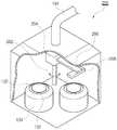
도 2는 본 발명에 따른 반도체 웨이퍼 현상 장치의 일 실시예를 도시한 부분 절개도이다.2 is a partial cutaway view showing an embodiment of a semiconductor wafer developing apparatus according to the present invention.
도 3은 본 발명에 따른 반도체 웨이퍼 현상 장치의 다른 실시예를 도시한 부분 절개도이다.3 is a partial cutaway view showing another embodiment of a semiconductor wafer developing apparatus according to the present invention.
도 4는 도 1에 도시된 현상 장치를 통해 현상된 웨이퍼의 선폭 평균값을 도시한 그래프이다.4 is a graph showing an average value of line widths of wafers developed by the developing apparatus of FIG. 1.
도 5는 도 2에 도시된 실시예를 통해 현상된 웨이퍼의 선폭 평균값을 도시한 그래프이다.FIG. 5 is a graph showing an average value of line widths of a wafer developed through the embodiment illustrated in FIG. 2.
<도면 중 주요 부분에 대한 부호의 설명><Explanation of symbols for main parts of the drawings>
102 : 챔버,102: chamber,
104 : 에어덕트,104: air duct,
110 : 슬라이드 바디,110: slide body,
112 : 가이드 레일,112: guide rail,
114 : 수직 아암,114: vertical arm,
116 : 수평 이동 기구,116: horizontal moving mechanism,
118 : 수평 아암,118: horizontal arm,
120 : 디스펜서 노즐,120: dispenser nozzle,
130 : 캐치 컵,130: catch cup,
132 : 스핀 척.132: spin chuck.
본 발명은 반도체 웨이퍼 현상 장치에 관한 것으로서, 보다 상세하게는 포토 리소그라피법에 의해 노광된 패턴을 현상하기 위한 현상 장치에 관한 것이다.BACKGROUND OF THE
반도체 제조 공정 중 포토리소그라피 공정은 웨이퍼 상에 원하는 패턴을 형성시키기 위한 공정으로서, 세척 및 건조를 마친 웨이퍼의 표면에 포토 레지스트와 같은 감광막을 균일하게 도포시키고, 그 위에 소정의 레이아웃을 갖는 포토 마스크 상의 특정 패턴에 따라 노광 공정을 수행한 후, 현상 공정에서 노광된 패턴 중 불필요한 부분을 제거하여 웨이퍼의 표면에 의도한 패턴을 형성시키는 공정을 의미한다.The photolithography process in the semiconductor manufacturing process is a process for forming a desired pattern on a wafer, and uniformly applying a photoresist film such as photoresist to the surface of the wafer after cleaning and drying, on a photomask having a predetermined layout thereon. After performing an exposure process according to a specific pattern, it means a process of forming an intended pattern on the surface of the wafer by removing unnecessary portions of the pattern exposed in the development process.
현상 공정에서는, 노광된 웨이퍼의 표면에 현상액을 분사하여 감광막의 특성에 따라서 노광된 부분 또는 그렇지 않은 부분이 현상액과 반응하여 웨이퍼 표면에 남거나 제거된다. 그 후, 순수(DI Water)를 분사하여 웨이퍼 표면을 세정하게 된다.In the developing step, the developer is sprayed onto the exposed wafer surface so that the exposed or unexposed portion is left or removed on the wafer surface in response to the developer, depending on the characteristics of the photosensitive film. Thereafter, DI water is sprayed to clean the wafer surface.
도 1은 종래의 현상 장치의 일예를 도시한 것이다. 상기 현상 장치는 공정 진행 중에 외부의 이물질로부터 웨이퍼를 차단하기 위한 챔버(10)를 포함하며, 상기 챔버(10)의 상부에는 외기를 유입하기 위한 에어덕트(12)가 설치되는 바, 상기 에어 덕트(12)의 단부에는 에어 필터(미도시)가 설치되어 먼지와 같은 이물질의 침입을 방지하게 된다.1 shows an example of a conventional developing apparatus. The developing apparatus includes a
한편, 상기 챔버(10)의 내부에는 웨이퍼의 표면에 현상액 및 세정액을 분사하기 위한 노즐(24)이 설치되며, 상기 노즐(24)은 수평 아암(22)의 단부에 고정되어 있다. 여기서, 상기 수평 아암(22)은 상기 노즐(24)을 웨이퍼 측으로 이송시키는 역할을 한다. 상기 수평 아암(22)의 일단부는 상기 챔버(10)의 바닥면으로부터 수직으로 설치되는 수직 아암(20)에 고정되며, 상기 노즐(24)은 도관(미도시)을 통해 현상액 및 세정액 저장조와 연결되어, 현상액 및 세정액을 웨이퍼 표면에 분사하게 된다.On the other hand, the inside of the
한편, 상기 수직 아암(20)의 일측에는 원통형의 캐치 컵(30)이 위치하며, 상기 캐치 컵(30)의 내부에는 회전축(34)에 연결된 스핀척(32)이 설치된다. 상기 스핀척(32)은 웨이퍼를 고정하는 역할을 하며, 상기 회전축(34)의 회전에 의해 웨이퍼가 고속으로 회전하면서 현상액의 도포, 세정 및 건조가 이루어진다.Meanwhile, a
여기서, 생산성 향상을 위해서 동일한 현상 장치를 두 개 이상 설치하는 것이 일반적이다. 동시에 두 곳 이상에서 공정을 진행할 수 있으므로 생산성이 증가 될 수 있으나, 안정적인 웨이퍼 수율을 얻기 위해서는 각각의 현상 장치에 있어서 현상 정도, 즉 선폭 및 선폭 균일도가 거의 동일해야만 한다.Here, in order to improve productivity, it is common to provide two or more of the same developing devices. Productivity can be increased because the process can be carried out at two or more places at the same time, but in order to obtain stable wafer yield, the degree of development, i.e., line width and line width uniformity, must be substantially the same in each developing apparatus.
그러나, 실질적으로 각각의 현상 장치의 기계적인 차이점이 존재할 수 밖에 없으므로 현상 정도에는 차이가 발생하게 된다. 현상 장치에 있어서, 이러한 선폭 및 선폭 균일도에 영향을 미치는 인자는 다음과 같다.However, since the mechanical differences between the respective developing apparatuses are inevitably existed, there is a difference in the degree of development. In the developing apparatus, factors affecting such line width and line width uniformity are as follows.
1. 챔버내 대기 조건(온도, 습도, 풍속)1. Ambient conditions in the chamber (temperature, humidity, wind speed)
2. 현상액의 화학적 온도2. Chemical temperature of developer
3. 현상액 노즐 상태3. Developer nozzle status
4. 회전 스피드4. Rotating Speed
5. 캐치 컵 내부의 상태5. Catch cup inside condition
6. 현상 레시피(recipe)6. Develop recipe
이외에도 다양한 요인이 있으나, 상기한 6개의 요인이 주요한 요인이 된다. 따라서, 상기 1 내지 5는 모두 현상 유닛의 기계적 조건에 관련된 것이어서, 각각 개별적인 챔버 내에서 현상 공정이 진행된 두 개의 웨이퍼에서 선폭 및 선폭 균일도를 동일하게 유지하는 것이 매우 어려운 문제점이 있다.There are various other factors, but the above six factors are the main factors. Therefore, the above 1 to 5 are all related to the mechanical conditions of the developing unit, and it is very difficult to maintain the same line width and line uniformity in the two wafers in which the developing process is performed in the respective chambers.
본 발명은 상기와 같은 종래 기술의 단점을 극복하기 위해 안출된 것으로서, 생산성을 저하시키지 않으면서도 동시에 현상 공정이 진행된 두 개 이상의 웨이퍼의 선폭 및 선폭 균일도와 같은 현상 정도를 거의 동일하게 유지시킬 수 있는 반도체 웨이퍼 현상 장치를 제공하는 것을 기술적 과제로 삼고 있다.The present invention has been made to overcome the disadvantages of the prior art as described above, it is possible to maintain the same degree of development, such as the line width and line width uniformity of two or more wafers at the same time the development process is performed without lowering the productivity It is a technical problem to provide a semiconductor wafer developing apparatus.
상기와 같은 기술적 과제를 달성하기 위하여 본 발명은, 챔버와; 상기 챔버 내부에 설치된 둘 이상의 캐치 컵과; 상기 각각의 캐치 컵 내부에 설치되며, 상부면에 웨이퍼가 고정되는 스핀 척과; 상기 스핀 척의 상부에서 상기 웨이퍼에 감광액 등을 분사하는 디스펜서 노즐을 포함하는 것을 특징으로 하는 반도체 웨이퍼 현상 장치를 제공한다.The present invention to achieve the above technical problem, the chamber; Two or more catch cups installed in the chamber; A spin chuck installed in each of the catch cups and having a wafer fixed to an upper surface thereof; It provides a semiconductor wafer developing apparatus comprising a dispenser nozzle for injecting a photosensitive liquid and the like on the wafer from the top of the spin chuck.
즉, 본 발명에서는 하나의 챔버 내에 두 개 이상의 캐치 컵을 설치하고 이를 통해 두 개 이상의 웨이퍼에 대해 동시에 현상 공정을 진행시킴으로써 각각의 웨이퍼에서 선폭 및 선폭 균일도와 같은 현상 정도를 균일하게 유지시킬 수 있도록 한 것이다.That is, in the present invention, by installing two or more catch cups in one chamber and simultaneously developing the two or more wafers, the development degree such as the line width and the line width uniformity in each wafer can be maintained uniformly. It is.
바람직하게는, 상기 스핀 척은 상기 다수의 스핀 척의 상부에 동시에 감광액 등을 분사하도록 하는 것이 좋다. 이를 통해, 챔버 내의 대기 조건 뿐만 아니라 현상액의 상태도 동일하게 유지할 수 있으므로 현상 정도를 보다 균일하게 유지할 수 있다.Preferably, the spin chuck may be configured to spray photoresist or the like on top of the plurality of spin chucks simultaneously. As a result, not only the atmospheric conditions but also the state of the developing solution in the chamber can be maintained the same, so that the degree of development can be maintained more uniformly.
여기서, 상기 디스펜서 노즐은 상기 다수의 스핀척의 상부를 가로질러서 배치되도록 할 수 있다. 즉, 디스펜서 노즐의 폭을 다수의 스핀척 모두의 상부에 배치될 수 있도록 연장함으로써 현상액 등의 분사조건을 동일하게 할 수 있다.Here, the dispenser nozzle may be arranged across the top of the plurality of spin chuck. In other words, by extending the width of the dispenser nozzle so that the width of the dispenser nozzle can be arranged above all of the plurality of spin chucks, the spraying conditions of the developer and the like can be made the same.
이외에도, 상기 디스펜서 노즐이 상기 각각의 스핀척의 상부에 위치할 수 있도록 하는 이동수단을 더 포함할 수도 있다. 즉, 하나의 웨이퍼에 대해 현상액을 분사한 후 디스펜서 노즐을 이동시켜 다른 웨이퍼에 대해 현상액을 분사하도록 하 는 것이다.In addition, the dispenser nozzle may further include a moving means to be positioned above the respective spin chuck. In other words, after the developer is sprayed on one wafer, the dispenser nozzle is moved to spray the developer on the other wafer.
상기 이동수단은 일단부에 상기 디스펜서 노즐이 장착되는 디스펜서 아암; 상기 아암의 타단부와 결합되며, 상기 챔버 저면에 회전 가능하게 설치되는 회전축을 포함하도록 할 수 있다. 또한, 상기 이동수단은 일단부에 상기 디스펜서 노즐이 장착되는 디스펜서 아암; 상기 아암의 타단부와 결합되며, 상기 챔버 저면에 슬라이드 가능하게 설치되는 슬라이드 바디를 포함할 수도 있다.The moving means may include a dispenser arm on which one end of the dispenser nozzle is mounted; It is coupled to the other end of the arm, it may be to include a rotating shaft rotatably installed on the bottom of the chamber. The moving unit may further include a dispenser arm having one end mounted with the dispenser nozzle; It may include a slide body coupled to the other end of the arm and slidably installed on the bottom of the chamber.
이하에서는, 첨부된 도면을 참조하여 본 발명에 따른 반도체 웨이퍼 현상 장치의 실시예에 대해 상세하게 설명하도록 한다.Hereinafter, with reference to the accompanying drawings will be described in detail an embodiment of a semiconductor wafer developing apparatus according to the present invention.
도 2를 참조하면, 본 발명에 따른 반도체 웨이퍼 현상 장치의 제1 실시예(100)의 챔버(102)는 기본적으로 도 1에 도시된 챔버와 동일한 형태를 갖는다. 물론, 상기 챔버(102)의 형태는 반드시 도시된 것에 한정되는 것은 아니며, 내부에 캐치 컵과 노즐 등이 설치될 수 있는 공간을 갖는 임의의 형태를 가질 수도 있다. 상기 챔버(102)의 상부에는 외기를 도입하기 위한 에어덕트(104)가 연결되어 상기 챔버(102)의 내부로 외기를 도입하여 건조 시간을 단축할 수 있게 한다.2, the
한편, 상기 챔버(102)의 바닥면에는 챔버(102)의 폭방향을 따라서 연장되는 가이드 레일(112)이 설치되며, 상기 가이드 레일(112)에는 슬라이드 바디(110)가 가이드 레일을 따라서 이동할 수 있도록 장착되어 있다. 상기 슬라이드 바디(110)는 내부에 구동 수단이 설치되어, 상기 실시예의 컨트롤러(미도시)의 제어에 따라 이동할 수 있다. 상기 슬라이드 바디(110)의 상부에는 수직 아암(114)이 상기 챔버 의 높이 방향으로 연장되게 설치되며, 상기 수직 아암(114)의 상부에는 수평 이동 기구(116)가 설치된다.Meanwhile, a
상기 수평 이동 기구(116)는 그 내부에 삽입되는 수평 아암(118)을 전진 또는 후퇴시키는 역할을 하며, 이로 인해 상기 수평 아암(118)이 후술할 캐치 컵쪽으로 이동하거나 홈 포지션(작동 초기 위치)으로 후퇴할 수 있게 된다. 상기 수평 아암(118)의 단부에는 디스펜서 노즐(120)이 설치된다. 상기 디스펜서 노즐(120)은 도시되지 않은 도관에 의해 현상액과 세정액 저장조와 연결되며, 상기 슬라이드 바디(110) 및 수평 이동 기구(116)에 의해 상기 챔버(102) 내에서 임의의 위치로 이동하여 현상액 및 세정액을 분사할 수 있게 된다.The
상기 가이드 레일(112)의 앞쪽에는 두 개의 캐치 컵(130)이 설치된다. 상기 캐치 컵(130)은 원통형의 형상을 가지며, 상단부는 내부에 저장되는 분사된 현상액 및 세정액이 외부로 누출되는 것을 방지하기 위해 중심을 향하여 절곡되어 있다. 상기 캐치 컵(130)의 중앙부에는 별도의 구동 수단(미도시)에 의해 회전되는 회전축(134) 상에 고정되는 스핀 척(132)이 설치된다. 상기 스핀 척(132)은 웨이퍼를 상면에 고정하여 고속으로 회전시키기 위한 것으로서, 상기 디스펜서 노즐(120)을 통해 분사된 현상액 및 세정액이 웨이퍼의 표면에 고르게 도포되도록 함과 동시에 보다 빠른 건조가 가능하도록 한다.Two catch cups 130 are installed at the front of the
따라서, 상기 실시예에 있어서는 동시에 두 개의 웨이퍼를 대상으로 하여 현상 공정을 진행할 수 있게 된다. 이때, 상술한 선폭 및 선폭 균일도와 같은 현상 정도에 영향을 미치는 기계적 요인 5가지 중 챔버내의 대기 조건은 동일한 상태에 서 현상이 이루어질 수 있으며, 상기 캐치 컵간의 거리를 짧게 설정하면 노즐 및 현상액의 상태도 거의 동일하게 가져갈 수 있어 두 개의 웨이퍼에서의 현상 정도의 차이를 최소화할 수 있게 된다.Therefore, in the above embodiment, the development process can be performed on two wafers at the same time. At this time, the atmospheric conditions in the chamber among the five mechanical factors affecting the degree of development such as the line width and the line width uniformity can be developed in the same state, and if the distance between the catch cup is set short, the state of the nozzle and developer The same can be taken to minimize the difference in the degree of development of the two wafers.
한편, 도시된 실시예 외에도, 상기 노즐을 좌우로 연장하여 슬라이드 바디를 움직이지 않고 고정된 상태에서 두 개에 웨이퍼에 대해서 동시에 현상액을 분사할 수 있도록 하는 실시예도 고려해 볼 수 있다. 또한, 도 2에서는 두 개의 캐치 컵이 도시되어 있으나, 그 이상의 캐치 컵이 설치되는 실시예도 고려해 볼 수 있다.On the other hand, in addition to the illustrated embodiment, it is also possible to consider an embodiment of extending the nozzle to the left and right so that the developer can be sprayed on two wafers at the same time in a fixed state without moving the slide body. In addition, although two catch cups are shown in FIG. 2, an embodiment in which more catch cups are installed may be considered.
도 3을 참조하면, 본 발명에 따른 반도체 웨이퍼 현상 장치의 제2 실시예가 도시되어 있다. 상기 제2 실시예(200)에서의 챔버(102) 및 에어덕트(104)는 도 2에 도시된 것을 채용할 수 있다. 마찬가지로, 상기 캐치 컵(130) 및 스핀 척(132) 또한, 동일한 것을 채용할 수 있다.3, a second embodiment of a semiconductor wafer developing apparatus according to the present invention is shown. The
한편, 상기 챔버(102)의 바닥면에는 수직 아암(202)이 설치되는바, 상기 수직 아암(202)은 모터와 같은 별도의 구동수단(미도시)에 의해 회전 가능하게 설치된다. 상기 수직 아암(202)의 상단부에는 수평 이동 기구(204)가 설치되어, 상기 수평 이동기구(204) 내에 설치된 수평 아암(206)을 전진 또는 후퇴시키도록 구성된다. 상기 수평 아암(206)의 단부에는 스핀 척(132)에 적재된 웨이퍼의 표면에 현상액 및 세정액을 분사하기 위한 디스펜서 노즐(208)이 설치된다.On the other hand, a
상기 실시예(200)에서는 상기 수직 아암(202)이 수평 이동하는 것이 아니라, 회전에 의해 각각의 캐치 컵(130)의 상부로 접근하게 된다. 이때, 상기 수평 이동 기구(204)에 의해 상기 디스펜서 노즐(208)의 스핀 척(132)에 고정된 웨이퍼 상부 로 이동하는데, 상기 수평 아암(206)의 길이를 조정하는 경우 수평 이동 기구(204)의 설치를 생략할 수도 있다.In the
도 3에 도시된 실시예에서는 두 개의 캐치 컵이 설치되어 있으나, 세 개 이상의 캐치 컵을 설치하는 실시예도 고려할 수 있다. 이 경우, 각각의 캐치 컵들은 상기 수직 아암을 중심으로 하는 원주 상에 배치되는 것이 좋다.Although two catch cups are installed in the embodiment shown in FIG. 3, an embodiment in which three or more catch cups are installed may be considered. In this case, the respective catch cups are preferably arranged on the circumference around the vertical arm.
한편, 도 4 및 도 5는 종래의 현상 장치와 도 2에 도시된 실시예에 의한 웨이퍼의 현상 정도를 도시한 것이다. 도 4에 도시된 바와 같이, 종래의 현상 장치에서는 각각의 현상 장치에서 현상된 웨이퍼의 선폭 평균값의 차이가 크지만, 도 5에 도시된 그래프에서는 그 차이가 현저하게 줄어든 것을 볼 수 있다.4 and 5 illustrate a development degree of the wafer according to the conventional developing apparatus and the embodiment shown in FIG. 2. As shown in FIG. 4, in the conventional developing apparatus, the difference in the line width average value of the wafer developed in each developing apparatus is large, but in the graph shown in FIG. 5, the difference is remarkably reduced.
상기와 같은 구성을 갖는 본 발명에 의하면, 선폭 및 선폭 균일도와 같은 현상 정도에 영향을 미치는 요인들을 서로 동일하게 유지하면서 두 개 이상의 웨이퍼에 대해서 현상 공정을 진행할 수 있으므로 생산성을 저하하지 않으면서도 각각의 웨이퍼에 대한 현상 정도를 거의 동일하게 유지할 수 있기 때문에 웨이퍼 수율을 높일 수 있는 효과를 제공한다.According to the present invention having the above-described configuration, the development process can be performed on two or more wafers while maintaining the same factors affecting the degree of development such as line width and line width uniformity, so that the productivity can be reduced without reducing productivity. Since the degree of development on the wafer can be maintained about the same, the wafer yield can be increased.
Claims (6)
Translated fromKoreanPriority Applications (1)
| Application Number | Priority Date | Filing Date | Title |
|---|---|---|---|
| KR1020040114250AKR100681315B1 (en) | 2004-12-28 | 2004-12-28 | Semiconductor wafer developing apparatus |
Applications Claiming Priority (1)
| Application Number | Priority Date | Filing Date | Title |
|---|---|---|---|
| KR1020040114250AKR100681315B1 (en) | 2004-12-28 | 2004-12-28 | Semiconductor wafer developing apparatus |
Publications (2)
| Publication Number | Publication Date |
|---|---|
| KR20060075458A KR20060075458A (en) | 2006-07-04 |
| KR100681315B1true KR100681315B1 (en) | 2007-02-15 |
Family
ID=37167995
Family Applications (1)
| Application Number | Title | Priority Date | Filing Date |
|---|---|---|---|
| KR1020040114250AExpired - Fee RelatedKR100681315B1 (en) | 2004-12-28 | 2004-12-28 | Semiconductor wafer developing apparatus |
Country Status (1)
| Country | Link |
|---|---|
| KR (1) | KR100681315B1 (en) |
Citations (2)
| Publication number | Priority date | Publication date | Assignee | Title |
|---|---|---|---|---|
| US5250114A (en)* | 1990-09-07 | 1993-10-05 | Tokyo Electron Limited | Coating apparatus with nozzle moving means |
| KR100186322B1 (en)* | 1996-05-22 | 1999-04-15 | 문정환 | Photoresist coater of semiconductor wafer |
- 2004
- 2004-12-28KRKR1020040114250Apatent/KR100681315B1/ennot_activeExpired - Fee Related
Patent Citations (2)
| Publication number | Priority date | Publication date | Assignee | Title |
|---|---|---|---|---|
| US5250114A (en)* | 1990-09-07 | 1993-10-05 | Tokyo Electron Limited | Coating apparatus with nozzle moving means |
| KR100186322B1 (en)* | 1996-05-22 | 1999-04-15 | 문정환 | Photoresist coater of semiconductor wafer |
Also Published As
| Publication number | Publication date |
|---|---|
| KR20060075458A (en) | 2006-07-04 |
Similar Documents
| Publication | Publication Date | Title |
|---|---|---|
| KR102000019B1 (en) | Unit for supplying liquid, Apparatus for treating a substrate, and Method for treating a substrate | |
| KR101512642B1 (en) | Developing processing method and developing apparatus | |
| KR101736441B1 (en) | Apparatus for treating substrate And method for cleaning guide plate | |
| US20120218531A1 (en) | Developing method and apparatus using organic-solvent containing developer | |
| KR101689619B1 (en) | Apparatus for treating substrate and System for treating substrate with the apparatus | |
| KR102359530B1 (en) | Method and Apparatus for treating substrate, and Method for cleaning cup | |
| US11845090B2 (en) | Nozzle apparatus, apparatus and method for treating substrate | |
| JP2004014844A (en) | Apparatus and method for treating substrate | |
| KR101769440B1 (en) | Method for treating substrate | |
| KR101985756B1 (en) | Apparatus and Method for treating substrate | |
| KR101884854B1 (en) | Apparatus and Method for treating substrate | |
| KR100681315B1 (en) | Semiconductor wafer developing apparatus | |
| CN109991820B (en) | Device and method for removing residual water drops after immersion exposure | |
| KR20200017027A (en) | Apparatus and Method for treating substrate | |
| KR20160141248A (en) | Apparatus and Method for treating substrate | |
| KR20130025133A (en) | Apparatus for treating substrate | |
| KR102223764B1 (en) | Apparatus and Method for treating substrate | |
| KR102010261B1 (en) | Apparatus and Method for treating a substrate | |
| KR101909185B1 (en) | Substrate treating apparatus and substrate treating method | |
| KR102330278B1 (en) | Method and Apparatus for treating substrate | |
| KR102289486B1 (en) | Apparatus and Method for treating substrate | |
| KR101985755B1 (en) | Apparatus and Method for treating a substrate | |
| KR20180061536A (en) | Substrate treating apparatus and substrate treating method | |
| KR20180122518A (en) | Apparatus for treating a substrate | |
| KR20180049309A (en) | Apparatus and Method for treating substrate |
Legal Events
| Date | Code | Title | Description |
|---|---|---|---|
| A201 | Request for examination | ||
| PA0109 | Patent application | St.27 status event code:A-0-1-A10-A12-nap-PA0109 | |
| PA0201 | Request for examination | St.27 status event code:A-1-2-D10-D11-exm-PA0201 | |
| R17-X000 | Change to representative recorded | St.27 status event code:A-3-3-R10-R17-oth-X000 | |
| D13-X000 | Search requested | St.27 status event code:A-1-2-D10-D13-srh-X000 | |
| D14-X000 | Search report completed | St.27 status event code:A-1-2-D10-D14-srh-X000 | |
| PN2301 | Change of applicant | St.27 status event code:A-3-3-R10-R13-asn-PN2301 St.27 status event code:A-3-3-R10-R11-asn-PN2301 | |
| PN2301 | Change of applicant | St.27 status event code:A-3-3-R10-R13-asn-PN2301 St.27 status event code:A-3-3-R10-R11-asn-PN2301 | |
| PG1501 | Laying open of application | St.27 status event code:A-1-1-Q10-Q12-nap-PG1501 | |
| E902 | Notification of reason for refusal | ||
| PE0902 | Notice of grounds for rejection | St.27 status event code:A-1-2-D10-D21-exm-PE0902 | |
| E13-X000 | Pre-grant limitation requested | St.27 status event code:A-2-3-E10-E13-lim-X000 | |
| P11-X000 | Amendment of application requested | St.27 status event code:A-2-2-P10-P11-nap-X000 | |
| P13-X000 | Application amended | St.27 status event code:A-2-2-P10-P13-nap-X000 | |
| R17-X000 | Change to representative recorded | St.27 status event code:A-3-3-R10-R17-oth-X000 | |
| E701 | Decision to grant or registration of patent right | ||
| PE0701 | Decision of registration | St.27 status event code:A-1-2-D10-D22-exm-PE0701 | |
| GRNT | Written decision to grant | ||
| PR0701 | Registration of establishment | St.27 status event code:A-2-4-F10-F11-exm-PR0701 | |
| PR1002 | Payment of registration fee | St.27 status event code:A-2-2-U10-U11-oth-PR1002 Fee payment year number:1 | |
| PG1601 | Publication of registration | St.27 status event code:A-4-4-Q10-Q13-nap-PG1601 | |
| LAPS | Lapse due to unpaid annual fee | ||
| PC1903 | Unpaid annual fee | St.27 status event code:A-4-4-U10-U13-oth-PC1903 Not in force date:20100206 Payment event data comment text:Termination Category : DEFAULT_OF_REGISTRATION_FEE | |
| PC1903 | Unpaid annual fee | St.27 status event code:N-4-6-H10-H13-oth-PC1903 Ip right cessation event data comment text:Termination Category : DEFAULT_OF_REGISTRATION_FEE Not in force date:20100206 |