KR100680958B1 - Manufacturing method of PMOS transistor - Google Patents
Manufacturing method of PMOS transistorDownload PDFInfo
- Publication number
- KR100680958B1 KR100680958B1KR1020050014860AKR20050014860AKR100680958B1KR 100680958 B1KR100680958 B1KR 100680958B1KR 1020050014860 AKR1020050014860 AKR 1020050014860AKR 20050014860 AKR20050014860 AKR 20050014860AKR 100680958 B1KR100680958 B1KR 100680958B1
- Authority
- KR
- South Korea
- Prior art keywords
- film
- hard mask
- gate
- substrate
- forming
- Prior art date
- Legal status (The legal status is an assumption and is not a legal conclusion. Google has not performed a legal analysis and makes no representation as to the accuracy of the status listed.)
- Expired - Fee Related
Links
Images


Classifications
- H—ELECTRICITY
- H10—SEMICONDUCTOR DEVICES; ELECTRIC SOLID-STATE DEVICES NOT OTHERWISE PROVIDED FOR
- H10D—INORGANIC ELECTRIC SEMICONDUCTOR DEVICES
- H10D62/00—Semiconductor bodies, or regions thereof, of devices having potential barriers
- H10D62/10—Shapes, relative sizes or dispositions of the regions of the semiconductor bodies; Shapes of the semiconductor bodies
- H10D62/17—Semiconductor regions connected to electrodes not carrying current to be rectified, amplified or switched, e.g. channel regions
- H10D62/213—Channel regions of field-effect devices
- H10D62/221—Channel regions of field-effect devices of FETs
- H10D62/235—Channel regions of field-effect devices of FETs of IGFETs
- H10D62/292—Non-planar channels of IGFETs
- H—ELECTRICITY
- H01—ELECTRIC ELEMENTS
- H01L—SEMICONDUCTOR DEVICES NOT COVERED BY CLASS H10
- H01L21/00—Processes or apparatus adapted for the manufacture or treatment of semiconductor or solid state devices or of parts thereof
- H01L21/02—Manufacture or treatment of semiconductor devices or of parts thereof
- H01L21/04—Manufacture or treatment of semiconductor devices or of parts thereof the devices having potential barriers, e.g. a PN junction, depletion layer or carrier concentration layer
- H01L21/18—Manufacture or treatment of semiconductor devices or of parts thereof the devices having potential barriers, e.g. a PN junction, depletion layer or carrier concentration layer the devices having semiconductor bodies comprising elements of Group IV of the Periodic Table or AIIIBV compounds with or without impurities, e.g. doping materials
- H01L21/28—Manufacture of electrodes on semiconductor bodies using processes or apparatus not provided for in groups H01L21/20 - H01L21/268
- H01L21/28008—Making conductor-insulator-semiconductor electrodes
- H01L21/28017—Making conductor-insulator-semiconductor electrodes the insulator being formed after the semiconductor body, the semiconductor being silicon
- H01L21/28026—Making conductor-insulator-semiconductor electrodes the insulator being formed after the semiconductor body, the semiconductor being silicon characterised by the conductor
- H01L21/28123—Lithography-related aspects, e.g. sub-lithography lengths; Isolation-related aspects, e.g. to solve problems arising at the crossing with the side of the device isolation; Planarisation aspects
- H—ELECTRICITY
- H01—ELECTRIC ELEMENTS
- H01L—SEMICONDUCTOR DEVICES NOT COVERED BY CLASS H10
- H01L21/00—Processes or apparatus adapted for the manufacture or treatment of semiconductor or solid state devices or of parts thereof
- H01L21/70—Manufacture or treatment of devices consisting of a plurality of solid state components formed in or on a common substrate or of parts thereof; Manufacture of integrated circuit devices or of parts thereof
- H01L21/71—Manufacture of specific parts of devices defined in group H01L21/70
- H01L21/76—Making of isolation regions between components
- H01L21/762—Dielectric regions, e.g. EPIC dielectric isolation, LOCOS; Trench refilling techniques, SOI technology, use of channel stoppers
- H01L21/76202—Dielectric regions, e.g. EPIC dielectric isolation, LOCOS; Trench refilling techniques, SOI technology, use of channel stoppers using a local oxidation of silicon, e.g. LOCOS, SWAMI, SILO
- H01L21/76205—Dielectric regions, e.g. EPIC dielectric isolation, LOCOS; Trench refilling techniques, SOI technology, use of channel stoppers using a local oxidation of silicon, e.g. LOCOS, SWAMI, SILO in a region being recessed from the surface, e.g. in a recess, groove, tub or trench region
- H—ELECTRICITY
- H10—SEMICONDUCTOR DEVICES; ELECTRIC SOLID-STATE DEVICES NOT OTHERWISE PROVIDED FOR
- H10D—INORGANIC ELECTRIC SEMICONDUCTOR DEVICES
- H10D62/00—Semiconductor bodies, or regions thereof, of devices having potential barriers
- H10D62/01—Manufacture or treatment
- H10D62/021—Forming source or drain recesses by etching e.g. recessing by etching and then refilling
Landscapes
- Engineering & Computer Science (AREA)
- Physics & Mathematics (AREA)
- Condensed Matter Physics & Semiconductors (AREA)
- General Physics & Mathematics (AREA)
- Manufacturing & Machinery (AREA)
- Computer Hardware Design (AREA)
- Microelectronics & Electronic Packaging (AREA)
- Power Engineering (AREA)
- Insulated Gate Type Field-Effect Transistor (AREA)
- Metal-Oxide And Bipolar Metal-Oxide Semiconductor Integrated Circuits (AREA)
Abstract
Translated fromKoreanDescription
Translated fromKorean도 1a 내지 도 1g는 본 발명에 따른 피모스 트랜지스터의 제조방법을 설명하기 위한 공정별 단면도.1A to 1G are cross-sectional views of processes for explaining a method of manufacturing a PMOS transistor according to the present invention.
도 2는 도 1c까지의 공정이 진행된 기판을 나타내는 평면도.FIG. 2 is a plan view showing a substrate on which the process up to FIG. 1C has been performed. FIG.
도 3은 도 1d까지의 공정이 진행된 기판을 나타내는 평면도.3 is a plan view showing a substrate on which the process up to FIG. 1D has been performed;
도 4는 도 3의 Ⅴ-Ⅵ(채널 폭 방향)을 따라 절단한 단면도.4 is a cross-sectional view taken along line V-VI (channel width direction) of FIG. 3;
도 5는 도 1f까지의 공정이 진행된 기판을 나타내는 평면도.FIG. 5 is a plan view illustrating a substrate on which the process of FIG. 1F is advanced; FIG.
도 6은 도 5의 Ⅸ-Ⅹ(채널 폭 방향)을 따라 절단한 단면도.FIG. 6 is a cross-sectional view taken along the line VII-VII (channel width direction) of FIG. 5; FIG.
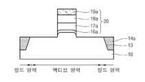
* 도면의 주요 부분에 대한 부호의 설명 *Explanation of symbols on the main parts of the drawings
10: 반도체 기판11: 패드 산화막10: semiconductor substrate 11: pad oxide film
12: 패드 질화막13: 트렌치12: pad nitride film 13: trench
14: 갭필 산화막15: 하드마스크막 형성용 산화막14: gap fill oxide film 15: oxide film for hard mask film formation
15a: 하드마스크막16,16a: 게이트 산화막15a:
17,17a: 도핑된 다결정실리콘막18,18a: 텅스텐 실리사이드막17,17a: doped polysilicon
19,19a: 게이트 하드마스크막20: 게이트19, 19a: gate hard mask layer 20: gate
21: 스페이서22: 소스 및 드레인 영역21: spacer 22: source and drain regions
본 발명은 반도체 소자의 제조방법에 관한 것이고, 특히, 페리(peri) 영역 피모스 트랜지스터의 유효 채널 길이를 증가시킬 수 있는 피모스 트랜지스터의 제조방법에 관한 것이다.The present invention relates to a method for manufacturing a semiconductor device, and more particularly, to a method for manufacturing a PMOS transistor capable of increasing the effective channel length of a peri region PMOS transistor.
최근, 반도체 소자의 디자인룰이 100 ㎚급 이하의 레벨로 감소됨에 따라, 페리 영역의 피모스 트랜지스터의 문턱전압(Vt) 마진 확보 및 오프 전류의 누설 감소가 중요한 문제로 대두되고 있다. 현재 페리 영역의 엔모스(NMOS) 및 피모스가 동시에 구현되어야 하는 씨모스(CMOS) 트랜지스터에 있어서, 피모스 트랜지스터의 경우 매립 채널을 통해 소자가 구현되며, 이는 캐리어 이동도가 커서 표면보다 더 큰 구동 전류를 얻을 수 있는 장점이 있지만, 채널 길이가 감소될수록 오프 전류의 특성 저하가 초래된다. 또한, 피모스 트랜지스터의 캐리어인 홀에 의해 부수적으로 생성되는 전자가 게이트 산화막 또는 소자분리막 내부로 주입된다. 이와 같이 주입되는 전자에 의해, 게이트의 턴-오프 시에도 피모스 트랜지스터의 채널이 인버전되면서 유효 채널의 길이가 감소되는 현상이 일어나며, 이러한 현상을 HEIP(hot electron induced punchthrough)라 한다. 상기 HEIP로 인해 기존에 발생되던 오프 전류가 더욱 증가되어 전력 소모가 증가되고, 동작 속도가 저하되며, 펀치쓰루 전압이 감소되는 등의 전기적 특성이 열화되는 문제가 있었다.In recent years, as the design rules of semiconductor devices have been reduced to a level of 100 nm or less, securing a threshold voltage (Vt) margin of the PMOS transistor in the ferry region and reducing the leakage of off current have emerged as important problems. In CMOS transistors where NMOS and PMOS in the ferry region must be implemented at the same time, in the case of a PMOS transistor, a device is implemented through a buried channel, which is larger than the surface due to the large carrier mobility. Although there is an advantage in that the driving current can be obtained, as the channel length is reduced, the characteristic of the off current is degraded. Also, electrons incidentally generated by holes that are carriers of the PMOS transistor are injected into the gate oxide film or the device isolation film. As a result of the electrons injected as described above, a phenomenon in which the effective channel length decreases as the PMOS transistor channel is inverted even when the gate is turned off, is called HEIP (hot electron induced punchthrough). Due to the HEIP, there is a problem in that electrical characteristics such as power consumption increase, operation speed decrease, and punch-through voltage are deteriorated due to an increase in the off current, which has been previously generated.
이러한 문제를 해결하기 위해 소자의 구조적 측면에서 여러가지 방안들이 제시되어 왔으며, 최근에는 게이트 라인 전체가 아닌 채널 감소가 발생하는 영역에 한하여 게이트 탭을 설치함으로써, 유효 채널 길이가 감소되는 것을 방지하기도 한다. 그러나, 반도체 소자의 디자인룰이 80 ㎚급 이하의 레벨로 감소되는 경우, 게이트 탭 설치를 위한 공간을 확보하기가 어렵기 때문에, HEIP로 인한 페리 영역 피모스 트랜지스터의 전기적 특성 열화를 극복하는데 한계가 있다.In order to solve this problem, various schemes have been proposed in terms of the structure of the device, and recently, by installing the gate tap only in a region where channel reduction occurs instead of the entire gate line, the effective channel length is prevented from being reduced. However, when the design rule of the semiconductor device is reduced to a level below 80 nm, since it is difficult to secure a space for the gate tap installation, there is a limit to overcome the deterioration of the electrical characteristics of the ferry region PMOS transistor due to HEIP. have.
따라서, 본 발명은 선행기술에 따른 피모스 트랜지스터의 제조방법에 내재되었던 상기한 바와 같은 문제점을 해결하기 위해 창작된 것으로서, 본 발명의 목적은, 피모스 트랜지스터의 채널 길이를 증가시켜, HEIP에 의해 감소되는 유효 채널 길이를 보상함으로써, 전기적 특성을 향상시킬 수 있는 피모스 트랜지스터의 제조방법을 제공함에 있다.Accordingly, the present invention was created to solve the above problems inherent in the method of manufacturing a PMOS transistor according to the prior art, and an object of the present invention is to increase the channel length of the PMOS transistor, The present invention provides a method of manufacturing a PMOS transistor capable of improving electrical characteristics by compensating for a reduced effective channel length.
상기 목적을 달성하기 위해, 본 발명의 일면에 따라, 피모스 트랜지스터의 제조방법이 제공되고: 이 방법은, 액티브 영역 및 필드 영역이 정의된 반도체 기판을 제공하는 단계; 상기 반도체 기판의 필드 영역에 소자분리막을 형성하는 단계; 상기 소자분리막이 형성된 반도체 기판 상에 채널 길이 방향으로 액티브 영역의 중앙부위를 덮되, 채널 폭 방향으로 액티브 영역의 중앙부위는 노출시키고, 양쪽 가장자리 및 이와 인접하는 필드 영역을 덮는 하드마스크막을 형성하는 단계; 상기 하드마스크막을 식각 장벽으로 이용하여 기판을 식각하여 리세스시키는 단계; 상기 하드마스크막을 제거하는 단계; 상기 하드마스크막의 제거가 완료된 기판 상에, 채널 길이 방향으로 액티브 영역의 중앙부위를 덮는 게이트를 형성하는 단계; 및 상 기 게이트 양측의 기판 표면 내에 소스 및 드레인 영역을 형성하는 단계;를 포함한다.In order to achieve the above object, according to one aspect of the present invention, there is provided a method of manufacturing a PMOS transistor, the method comprising: providing a semiconductor substrate having an active region and a field region defined; Forming an isolation layer in the field region of the semiconductor substrate; Forming a hard mask layer on the semiconductor substrate on which the device isolation layer is formed, covering a central portion of the active region in a channel length direction, exposing a central portion of the active region in a channel width direction, and covering both edges and adjacent field regions; ; Etching and recessing a substrate using the hard mask layer as an etch barrier; Removing the hard mask layer; Forming a gate covering a central portion of the active region in a channel length direction on the substrate on which the hard mask film is removed; And forming source and drain regions in the substrate surfaces on both sides of the gate.
본 발명의 다른 일면에 따라, 상기 소자분리막을 형성하는 단계;는, 상기 액티브 영역 및 필드 영역이 정의된 반도체 기판 상에 필드 영역을 노출시키는 패드 산화막 및 패드 질화막을 차례로 형성하는 단계; 상기 패드 질화막을 식각 장벽으로 이용하여 기판을 식각하여 트렌치를 형성하는 단계; 결과물 상에 상기 트렌치를 매립하도록 갭필 산화막을 형성하는 단계; 상기 패드 질화막이 노출될 때까지 갭필 산화막을 씨엠피하는 단계; 및 상기 씨엠피후 잔류된 패드 질화막 및 패드 산화막을 제거하는 단계;를 포함한다.According to another aspect of the present invention, the forming of the device isolation film may include: sequentially forming a pad oxide film and a pad nitride film exposing a field region on a semiconductor substrate in which the active region and the field region are defined; Etching the substrate using the pad nitride layer as an etch barrier to form a trench; Forming a gapfill oxide layer on the resultant to fill the trench; CMPing the gapfill oxide layer until the pad nitride layer is exposed; And removing the pad nitride film and the pad oxide film remaining after the CMP.
본 발명의 다른 일면에 따라, 상기 패드 산화막의 두께는 50~150 Å이다.According to another aspect of the invention, the thickness of the pad oxide film is 50 to 150 kPa.
본 발명의 다른 일면에 따라, 상기 패드 질화막의 두께는 500~700 Å이다.According to another aspect of the invention, the thickness of the pad nitride film is 500 ~ 700 Å.
본 발명의 다른 일면에 따라, 상기 트렌치의 깊이는 2,000~3,000 Å이다.According to another aspect of the invention, the depth of the trench is 2,000-3,000 mm 3.
본 발명의 다른 일면에 따라, 상기 하드마스크막은 산화막이다.According to another aspect of the invention, the hard mask film is an oxide film.
본 발명의 다른 일면에 따라, 상기 하드마스크막은 50~100 Å의 두께로 형성된다.According to another aspect of the invention, the hard mask film is formed to a thickness of 50 ~ 100Å.
본 발명의 다른 일면에 따라, 상기 기판의 리세스 공정은 400~600 Å의 깊이만큼 수행한다.According to another aspect of the invention, the recess process of the substrate is performed by a depth of 400 ~ 600 Å.
본 발명의 다른 일면에 따라, 상기 게이트는 게이트 산화막, 도핑된 다결정실리콘막, 텅스텐 실리사이드막 및 게이트 하드마스크막을 차례로 적층시켜 형성한다.According to another aspect of the present invention, the gate is formed by sequentially stacking a gate oxide film, a doped polysilicon film, a tungsten silicide film, and a gate hard mask film.
본 발명의 다른 일면에 따라, 상기 게이트 산화막의 두께는 30~50 Å이다.According to another aspect of the invention, the thickness of the gate oxide film is 30 to 50 kPa.
본 발명의 다른 일면에 따라, 상기 도핑된 다결정실리콘막의 두께는 400~700 Å이다.According to another aspect of the invention, the thickness of the doped polysilicon film is 400 ~ 700 Å.
본 발명의 다른 일면에 따라, 상기 텅스텐 실리사이드막의 두께는 1,000~1,500 Å이다.According to another aspect of the invention, the thickness of the tungsten silicide film is 1,000 to 1,500 kPa.
본 발명의 또 다른 일면에 따라, 상기 게이트 하드마스크막의 두께는 2,000~2,500 Å이다.According to another aspect of the present invention, the gate hard mask layer has a thickness of 2,000 to 2,500 Pa.
(실시예)(Example)
이하, 첨부한 도면을 참조하여 본 발명의 바람직한 실시예를 상술하기로 한다.Hereinafter, exemplary embodiments of the present invention will be described in detail with reference to the accompanying drawings.
도 1a 내지 도 1g는 본 발명에 따른 피모스 트랜지스터의 제조방법을 설명하기 위한 공정별 단면도이다.1A to 1G are cross-sectional views of processes for describing a method of manufacturing a PMOS transistor according to the present invention.
먼저, 도 1a에 도시한 바와 같이, 액티브 영역 및 필드 영역이 정의된 반도체 기판(10)을 제공한다. 그런 다음, 상기 반도체 기판(10) 상에 필드 영역을 노출시키는 패드 산화막(11) 및 패드 질화막(12)을 차례로 형성한다. 패드 산화막(11)의 두께는 50~150 Å이고, 패드 질화막(12)의 두께는 500~700 Å이다. 이어서, 패드 질화막(12)을 식각 장벽으로 이용하여 기판(10)을 식각하여 트렌치(13)를 형성한다. 트렌치(13)의 깊이는 2,000~3,000 Å이다. 그리고 나서, 결과물 상에 트렌치(13)를 매립하도록 갭필 산화막(14)을 형성한다.First, as shown in FIG. 1A, a
도 1b에 도시한 바와 같이, 패드 질화막(12)이 노출될 때까지 갭필 산화막 (14)을 씨엠피(chemical mechanical polishing: CMP)한 다음, 씨엠피후 잔류된 패드 질화막(12) 및 패드 산화막(11)을 제거하여 소자분리막(14a)을 형성한다. 그리고나서, 소자분리막(14a)이 형성된 반도체 기판(10) 상에 하드마스크막 형성용 산화막(15)을 형성한다. 하드마스크막 형성용 산화막(15)은 50~100 Å의 두께로 형성한다.As shown in FIG. 1B, the gap
도 1c 및 도 2에 도시한 바와 같이, 하드마스크막 형성용 산화막(15)을 선택적으로 식각하여, 채널 길이 방향으로 액티브 영역의 중앙부위를 덮되, 채널 폭 방향으로 액티브 영역의 중앙부위는 노출시키고, 양쪽 가장자리 및 이와 인접하는 필드 영역을 덮는 하드마스크막(15a)을 형성한다. 이때, 도 2는 도 1c까지의 공정이 진행된 기판을 나타내는 평면도이고, 도 1c는 도 2의 Ⅰ- Ⅱ(채널 길이 방향)을 따라 절단한 단면도이다. 도 2에서 미설명한 도면부호 W는 액티브 영역을 덮는 하드마스크막(15a)의 폭(width)을 나타낸다. 이 폭(W)의 크기는 상기 하드마스크막 형성용 산화막(15)의 식각 공정시에 조절이 가능하다.As shown in FIGS. 1C and 2, the hard mask film forming
도 1d, 도 3 및 도 4에 도시한 바와 같이, 하드마스크막(15a)을 식각 장벽으로 이용하여 기판(10)을 식각하여 리세스시킨다. 상기 기판(10)의 리세스 공정은 400~600 Å의 깊이만큼 수행한다. 여기서, 도 3은 도 1d까지의 공정이 진행된 기판을 나타내는 평면도이고, 도 4는 도 3의 Ⅴ-Ⅵ(채널 폭 방향)을 따라 절단한 단면도이다. 또한, 도 1d는 도 3의 Ⅲ-Ⅳ(채널 길이 방향)을 따라 절단한 단면도이다. 상기 리세스 공정이 수행됨에 따라, 채널 길이 방향 및 채널 폭 방향으로 채널의 길이가 증가된다. 따라서, 상기와 같이 하면 종래의 게이트 탭 구조 적용시 에 나타나는 공정적 마진의 한계를 극복할 수 있고, 피모스 트랜지스터의 동작에 필요한 채널 길이를 확보함으로써, 게이트 턴 오프 시에 발생되는 오프 전류를 현저히 감소시켜 동작 전압 손실을 최소화할 수 있다.As shown in FIGS. 1D, 3, and 4, the
또한, 상기 리세스 공정에 의해 증가되는 채널의 길이는, 액티브 영역을 덮는 하드마스크막(15a)의 폭(W) 및 기판(10)의 리세스 깊이에 의해 조절이 가능하다. 이로써, HEIP에 의한 유효 채널 길이의 감소효과가 크더라도, 상기 폭(W) 및 리세스 깊이를 조절하여, 원하는 만큼의 채널 길이를 얻을 수 있으므로, HEIP에 의한 유효 채널 길이 감소분에 대해 충분한 보상이 가능하다. 결국, HEIP로 인한 문턱 전압 감소 및 오프 전류 증가를 방지할 수 있다. 따라서, 펀치쓰루 전압 및 전력 소모를 감소시킬 수 있고, 동작 속도를 향상시킬 수 있다.In addition, the length of the channel increased by the recess process may be adjusted by the width W of the
이후, 하드마스크막(15a)을 제거한다. 이때, 도 3에서 미설명한 도면부호 A는 리세스되지 않은 영역을 나타낸다. 그런 다음, 도면에 도시하지는 않았지만, 하드마스크막(15a)의 제거가 완료된 기판(10) 상에 스크린 산화막(도시안됨)을 형성하고 나서, 웰 이온주입 및 채널 이온주입 공정을 차례로 수행한다. 그리고 나서, 스크린 산화막을 제거한다.Thereafter, the
도 1e에 도시한 바와 같이, 이로부터 얻어지는 기판(10) 상에 게이트 산화막(16), 도핑된 다결정실리콘막(17), 텅스텐 실리사이드막(18) 및 게이트 하드마스크막(19)을 차례로 형성한다. 게이트 산화막(16)은 30~50 Å의 두께로 형성하고, 도핑된 다결정실리콘막(17)은 400~700 Å의 두께로 형성한다. 또한, 텅스텐 실리사이드막(18)은 1,000~1,500 Å의 두께로 형성하고, 게이트 하드마스크막(19)은 2,000~2,500 Å의 두께로 형성한다.As shown in FIG. 1E, a
도 1f, 도 5 및 도 6에 도시한 바와 같이, 게이트 하드마스크막(19), 텅스텐 실리사이드막(18), 도핑된 다결정실리콘막(17) 및 게이트 산화막(16)을 선택적으로 식각하여 채널 길이 방향으로 액티브 영역의 중앙부위를 덮는 게이트(20)를 형성한다. 여기서, 도 5는 도 1f까지의 공정이 진행된 기판을 나타내는 평면도이고, 도 6은 도 5의 Ⅸ-Ⅹ(채널 폭 방향)을 따라 절단한 단면도이며, 도 1f는 도 5의 Ⅶ-Ⅷ(채널 길이 방향)을 따라 절단한 단면도이다. 도 1f 및 도 6에서 미설명한 도면부호 16a는 식각후 잔류된 게이트 산화막을 나타내고, 17a는 식각후 잔류된 도핑된 다결정실리콘막을 나타내고, 18a는 식각후 잔류된 텅스텐 실리사이드막을 나타내며, 19a는 식각후 잔류된 게이트 하드마스크막을 나타낸다.1F, 5, and 6, the gate
도 1g에 도시한 바와 같이, 게이트(20)의 양측벽에 스페이서(21)를 형성하고, 스페이서(21)를 포함한 게이트(20) 양측의 기판(10) 표면 내에 P형 불순물을 이온주입하여 소오스 및 드레인 영역(22)을 형성한다.As shown in FIG. 1G,
본 발명을 특정의 바람직한 실시예에 관련하여 도시하고 설명하였지만, 본 발명이 그에 한정되는 것은 아니고 이하의 특허청구의 범위에 의해 마련되는 본 발명의 정신이나 분야를 이탈하지 않는 한도 내에서 본 발명이 다양하게 개조 및 변화될 수 있다는 것을 당 업계에서 통상의 지식을 가진 자는 용이하게 알 수 있다.While the invention has been shown and described with respect to certain preferred embodiments thereof, the invention is not so limited and it is intended that the invention be limited without departing from the spirit or field of the invention as set forth in the following claims It will be readily apparent to one of ordinary skill in the art that various modifications and variations can be made.
본 발명의 상기한 바와 같은 구성에 따라, 소자분리막이 구비된 반도체 기판 상에 채널 길이 방향으로 액티브 영역의 중앙부위를 덮되, 채널 폭 방향으로 액티 브 영역의 중앙부위는 노출시키고, 양쪽 가장자리 및 이와 인접하는 필드 영역을 덮는 하드마스크막을 형성하고, 상기 하드마스크막에 의해 노출된 기판 부분을 식각하여 리세스시킴으로써, 채널 길이 방향은 물론, 채널 폭 방향으로 채널의 길이를 증가시킬 수 있다. 따라서, 종래의 게이트 탭 구조 적용시에 나타나는 공정적 마진의 한계를 극복할 수 있고, HEIP에 의한 유효 채널의 길이 감소분을 보상할 수 있다. 이에 따라, 문턱 전압의 감소 및 오프 전류의 증가를 방지할 수 있으므로, 펀치쓰루 전압 및 전력 소모를 감소시킬 수 있고, 동작 속도를 향상시킬 수 있다.According to the above-described configuration of the present invention, the center portion of the active region is covered in the channel length direction on the semiconductor substrate provided with the device isolation film, but the center portion of the active region is exposed in the channel width direction, and both edges and the same are exposed. The length of the channel can be increased in the channel width direction as well as the channel length direction by forming a hard mask film covering the adjacent field region and etching the recessed portion of the substrate exposed by the hard mask film. Therefore, it is possible to overcome the limitation of the process margin shown in the conventional gate tap structure application, and to compensate for the length reduction of the effective channel by HEIP. Accordingly, it is possible to prevent the reduction of the threshold voltage and the increase of the off current, so that the punch-through voltage and power consumption can be reduced, and the operation speed can be improved.
결과적으로, 본 발명은 트랜지스터의 전기적 특성을 향상시킬 수 있다.As a result, the present invention can improve the electrical characteristics of the transistor.
Claims (13)
Translated fromKoreanPriority Applications (3)
| Application Number | Priority Date | Filing Date | Title |
|---|---|---|---|
| KR1020050014860AKR100680958B1 (en) | 2005-02-23 | 2005-02-23 | Manufacturing method of PMOS transistor |
| US11/302,055US7468301B2 (en) | 2005-02-23 | 2005-12-12 | PMOS transistor with increased effective channel length in the peripheral region and a multi-height substrate |
| US12/272,011US7808057B2 (en) | 2005-02-23 | 2008-11-17 | PMOS transistor with increased effective channel length in the peripheral region and method of manufacturing the same |
Applications Claiming Priority (1)
| Application Number | Priority Date | Filing Date | Title |
|---|---|---|---|
| KR1020050014860AKR100680958B1 (en) | 2005-02-23 | 2005-02-23 | Manufacturing method of PMOS transistor |
Publications (2)
| Publication Number | Publication Date |
|---|---|
| KR20060094159A KR20060094159A (en) | 2006-08-29 |
| KR100680958B1true KR100680958B1 (en) | 2007-02-09 |
Family
ID=36911790
Family Applications (1)
| Application Number | Title | Priority Date | Filing Date |
|---|---|---|---|
| KR1020050014860AExpired - Fee RelatedKR100680958B1 (en) | 2005-02-23 | 2005-02-23 | Manufacturing method of PMOS transistor |
Country Status (2)
| Country | Link |
|---|---|
| US (2) | US7468301B2 (en) |
| KR (1) | KR100680958B1 (en) |
Families Citing this family (13)
| Publication number | Priority date | Publication date | Assignee | Title |
|---|---|---|---|---|
| US7569434B2 (en)* | 2006-01-19 | 2009-08-04 | International Business Machines Corporation | PFETs and methods of manufacturing the same |
| KR100927403B1 (en)* | 2007-10-08 | 2009-11-19 | 주식회사 하이닉스반도체 | Semiconductor device and manufacturing method |
| US9543434B2 (en) | 2011-05-19 | 2017-01-10 | Hewlett-Packard Development Company, L.P. | Device active channel length/width greater than channel length/width |
| US8994082B2 (en)* | 2011-09-30 | 2015-03-31 | Taiwan Semiconductor Manufacturing Company, Ltd. | Transistors, methods of manufacturing thereof, and image sensor circuits with reduced RTS noise |
| US9355888B2 (en)* | 2012-10-01 | 2016-05-31 | Taiwan Semiconductor Manufacturing Company, Ltd. | Implant isolated devices and method for forming the same |
| CN104103319B (en)* | 2013-04-11 | 2017-08-25 | 中芯国际集成电路制造(上海)有限公司 | Anti-fuse circuit and its programmed method, anti-fuse structures |
| KR20140134068A (en) | 2013-05-13 | 2014-11-21 | 에스케이하이닉스 주식회사 | Spin transistor, and semiconductor device, memory device, microprocessor, processor, system, data storage system and memory system including the spin transistor |
| US11351437B2 (en)* | 2014-05-16 | 2022-06-07 | Jin Song | Impedance-based impact determination and scoring |
| US11844989B2 (en)* | 2019-12-09 | 2023-12-19 | Jin Song | Impact sensor embedded protector with nine-axis inertial measurement unit for scoring combative sports |
| CN104240762B (en)* | 2013-06-09 | 2018-06-01 | 中芯国际集成电路制造(上海)有限公司 | Anti-fuse structures and programmed method |
| KR102191909B1 (en)* | 2014-02-17 | 2020-12-18 | 에스케이하이닉스 주식회사 | Anti-fuse and method for fabricating the same |
| JP2017069231A (en)* | 2015-09-28 | 2017-04-06 | ソニー株式会社 | Mos field effect transistor, semiconductor integrated circuit, solid-state image sensor, and electronic apparatus |
| US12161927B2 (en)* | 2022-05-05 | 2024-12-10 | Jin Song | Impedance-based impact determination and scoring |
Citations (2)
| Publication number | Priority date | Publication date | Assignee | Title |
|---|---|---|---|---|
| JPH07302902A (en)* | 1994-05-10 | 1995-11-14 | Toshiba Corp | Semiconductor device |
| JP2002313950A (en)* | 2001-04-16 | 2002-10-25 | Sharp Corp | Semiconductor device and manufacturing method thereof |
Family Cites Families (28)
| Publication number | Priority date | Publication date | Assignee | Title |
|---|---|---|---|---|
| JP2994670B2 (en)* | 1989-12-02 | 1999-12-27 | 忠弘 大見 | Semiconductor device and manufacturing method thereof |
| US5396096A (en)* | 1992-10-07 | 1995-03-07 | Matsushita Electric Industrial Co., Ltd. | Semiconductor device and manufacturing method thereof |
| JP2800702B2 (en)* | 1994-10-31 | 1998-09-21 | 日本電気株式会社 | Semiconductor device |
| JP3380086B2 (en)* | 1995-05-26 | 2003-02-24 | 三菱電機株式会社 | Method for manufacturing semiconductor device |
| JP4027447B2 (en)* | 1996-04-24 | 2007-12-26 | 株式会社ルネサステクノロジ | Manufacturing method of semiconductor device |
| JPH118387A (en)* | 1997-06-18 | 1999-01-12 | Mitsubishi Electric Corp | Semiconductor device and manufacturing method thereof |
| US5998848A (en)* | 1998-09-18 | 1999-12-07 | International Business Machines Corporation | Depleted poly-silicon edged MOSFET structure and method |
| JP3383244B2 (en)* | 1999-09-29 | 2003-03-04 | シャープ株式会社 | Semiconductor transistor and method of manufacturing the same |
| JP3472738B2 (en)* | 1999-12-24 | 2003-12-02 | Necエレクトロニクス株式会社 | Circuit manufacturing method, semiconductor device |
| JP3716406B2 (en)* | 2000-02-08 | 2005-11-16 | 富士通株式会社 | Insulated gate semiconductor device and manufacturing method thereof |
| JP4592193B2 (en)* | 2001-02-06 | 2010-12-01 | ルネサスエレクトロニクス株式会社 | Manufacturing method of semiconductor device |
| US6611231B2 (en)* | 2001-04-27 | 2003-08-26 | Vivato, Inc. | Wireless packet switched communication systems and networks using adaptively steered antenna arrays |
| JP4790166B2 (en)* | 2001-07-05 | 2011-10-12 | Okiセミコンダクタ株式会社 | Protection transistor |
| US6744094B2 (en)* | 2001-08-24 | 2004-06-01 | Micron Technology Inc. | Floating gate transistor with horizontal gate layers stacked next to vertical body |
| US6921690B2 (en)* | 2001-12-20 | 2005-07-26 | Intersil Americas Inc. | Method of fabricating enhanced EPROM structures with accentuated hot electron generation regions |
| JP2003318405A (en)* | 2002-04-25 | 2003-11-07 | Mitsubishi Electric Corp | Semiconductor device and method of manufacturing the same |
| JP4546021B2 (en)* | 2002-10-02 | 2010-09-15 | ルネサスエレクトロニクス株式会社 | Insulated gate field effect transistor and semiconductor device |
| US6833569B2 (en)* | 2002-12-23 | 2004-12-21 | International Business Machines Corporation | Self-aligned planar double-gate process by amorphization |
| US6887798B2 (en)* | 2003-05-30 | 2005-05-03 | International Business Machines Corporation | STI stress modification by nitrogen plasma treatment for improving performance in small width devices |
| US6936881B2 (en)* | 2003-07-25 | 2005-08-30 | Taiwan Semiconductor Manufacturing Company, Ltd. | Capacitor that includes high permittivity capacitor dielectric |
| KR101158708B1 (en)* | 2004-05-06 | 2012-06-22 | 코닌클리케 필립스 일렉트로닉스 엔.브이. | Communication system, primary station and method of transmit power control |
| US20060247505A1 (en)* | 2005-04-28 | 2006-11-02 | Siddiqui Waqaas A | Wireless sensor system |
| GB2429605B (en)* | 2005-08-24 | 2008-06-04 | Ipwireless Inc | Apparatus and method for communicating signalling information |
| WO2007031961A2 (en)* | 2005-09-16 | 2007-03-22 | Koninklijke Philips Electronics, N.V. | Method of recovering communication access in dynamic spectrum access wireless systems |
| EP1929827A2 (en)* | 2005-09-16 | 2008-06-11 | Koninklijke Philips Electronics N.V. | Spectrum management in dynamic spectrum access wireless systems |
| US7616604B2 (en)* | 2005-10-25 | 2009-11-10 | Cisco Technology, Inc. | Identifying one or more access points in one or more channels to facilitate communication |
| KR100639220B1 (en)* | 2005-12-01 | 2006-11-01 | 주식회사 하이닉스반도체 | Semiconductor device and manufacturing method thereof |
| ATE526801T1 (en)* | 2006-01-11 | 2011-10-15 | Qualcomm Inc | COMMUNICATION METHOD AND APPARATUS FOR SENDING PRIORITY INFORMATION VIA BEACON SIGNALS |
- 2005
- 2005-02-23KRKR1020050014860Apatent/KR100680958B1/ennot_activeExpired - Fee Related
- 2005-12-12USUS11/302,055patent/US7468301B2/enactiveActive
- 2008
- 2008-11-17USUS12/272,011patent/US7808057B2/enactiveActive
Patent Citations (2)
| Publication number | Priority date | Publication date | Assignee | Title |
|---|---|---|---|---|
| JPH07302902A (en)* | 1994-05-10 | 1995-11-14 | Toshiba Corp | Semiconductor device |
| JP2002313950A (en)* | 2001-04-16 | 2002-10-25 | Sharp Corp | Semiconductor device and manufacturing method thereof |
Non-Patent Citations (2)
| Title |
|---|
| 07302902 * |
| 14313950 * |
Also Published As
| Publication number | Publication date |
|---|---|
| US7468301B2 (en) | 2008-12-23 |
| KR20060094159A (en) | 2006-08-29 |
| US20060186487A1 (en) | 2006-08-24 |
| US7808057B2 (en) | 2010-10-05 |
| US20090072280A1 (en) | 2009-03-19 |
Similar Documents
| Publication | Publication Date | Title |
|---|---|---|
| KR100523310B1 (en) | Semiconductor device | |
| US7122876B2 (en) | Isolation-region configuration for integrated-circuit transistor | |
| US8183626B2 (en) | High-voltage MOS devices having gates extending into recesses of substrates | |
| US7808057B2 (en) | PMOS transistor with increased effective channel length in the peripheral region and method of manufacturing the same | |
| US20090278196A1 (en) | FinFETs having dielectric punch-through stoppers | |
| US20090072310A1 (en) | Semiconductor structure including high voltage device | |
| US7514747B2 (en) | Silicon-on-insulator semiconductor device | |
| KR100457222B1 (en) | Method of manufacturing high voltage device | |
| US7394120B2 (en) | Semiconductor device having a shaped gate electrode and method of manufacturing the same | |
| KR100840659B1 (en) | Manufacturing method of dimos device | |
| KR100929635B1 (en) | Vertical transistor and method of formation thereof | |
| KR100424414B1 (en) | Method for forming high voltage transistor | |
| JP2008066548A (en) | Semiconductor device and manufacturing method of semiconductor device | |
| KR100282453B1 (en) | Method for manufacturing semiconductor device the same | |
| KR100848242B1 (en) | Semiconductor device and manufacturing method of semiconductor device | |
| US20110024837A1 (en) | Semiconductor device and method for fabricating the same | |
| KR100464535B1 (en) | A method for forming a transistor of a semiconductor device | |
| KR100713917B1 (en) | Method for manufacturing PMOS transistor | |
| US20220320328A1 (en) | Transistor structure and processing method therefore | |
| JP2005175011A (en) | Field effect transistor and its manufacturing method | |
| KR100609532B1 (en) | Manufacturing Method of SOI Semiconductor Device | |
| KR20070076815A (en) | PMOS transistor and its formation method | |
| US20120135572A1 (en) | Semiconductor device manufacturing method | |
| KR20050059749A (en) | Method of manufacturing semiconductor device | |
| KR20040015594A (en) | Method for forming mos transistor of semiconductor device |
Legal Events
| Date | Code | Title | Description |
|---|---|---|---|
| A201 | Request for examination | ||
| PA0109 | Patent application | St.27 status event code:A-0-1-A10-A12-nap-PA0109 | |
| PA0201 | Request for examination | St.27 status event code:A-1-2-D10-D11-exm-PA0201 | |
| PG1501 | Laying open of application | St.27 status event code:A-1-1-Q10-Q12-nap-PG1501 | |
| E902 | Notification of reason for refusal | ||
| PE0902 | Notice of grounds for rejection | St.27 status event code:A-1-2-D10-D21-exm-PE0902 | |
| E701 | Decision to grant or registration of patent right | ||
| PE0701 | Decision of registration | St.27 status event code:A-1-2-D10-D22-exm-PE0701 | |
| GRNT | Written decision to grant | ||
| PR0701 | Registration of establishment | St.27 status event code:A-2-4-F10-F11-exm-PR0701 | |
| PR1002 | Payment of registration fee | St.27 status event code:A-2-2-U10-U11-oth-PR1002 Fee payment year number:1 | |
| PG1601 | Publication of registration | St.27 status event code:A-4-4-Q10-Q13-nap-PG1601 | |
| PR1001 | Payment of annual fee | St.27 status event code:A-4-4-U10-U11-oth-PR1001 Fee payment year number:4 | |
| PR1001 | Payment of annual fee | St.27 status event code:A-4-4-U10-U11-oth-PR1001 Fee payment year number:5 | |
| FPAY | Annual fee payment | Payment date:20120126 Year of fee payment:6 | |
| PR1001 | Payment of annual fee | St.27 status event code:A-4-4-U10-U11-oth-PR1001 Fee payment year number:6 | |
| PN2301 | Change of applicant | St.27 status event code:A-5-5-R10-R13-asn-PN2301 St.27 status event code:A-5-5-R10-R11-asn-PN2301 | |
| PN2301 | Change of applicant | St.27 status event code:A-5-5-R10-R13-asn-PN2301 St.27 status event code:A-5-5-R10-R11-asn-PN2301 | |
| LAPS | Lapse due to unpaid annual fee | ||
| PC1903 | Unpaid annual fee | St.27 status event code:A-4-4-U10-U13-oth-PC1903 Not in force date:20130203 Payment event data comment text:Termination Category : DEFAULT_OF_REGISTRATION_FEE | |
| PC1903 | Unpaid annual fee | St.27 status event code:N-4-6-H10-H13-oth-PC1903 Ip right cessation event data comment text:Termination Category : DEFAULT_OF_REGISTRATION_FEE Not in force date:20130203 | |
| PN2301 | Change of applicant | St.27 status event code:A-5-5-R10-R13-asn-PN2301 St.27 status event code:A-5-5-R10-R11-asn-PN2301 | |
| P22-X000 | Classification modified | St.27 status event code:A-4-4-P10-P22-nap-X000 |