KR100680940B1 - Metal wiring formation method of semiconductor device - Google Patents
Metal wiring formation method of semiconductor deviceDownload PDFInfo
- Publication number
- KR100680940B1 KR100680940B1KR1020000084171AKR20000084171AKR100680940B1KR 100680940 B1KR100680940 B1KR 100680940B1KR 1020000084171 AKR1020000084171 AKR 1020000084171AKR 20000084171 AKR20000084171 AKR 20000084171AKR 100680940 B1KR100680940 B1KR 100680940B1
- Authority
- KR
- South Korea
- Prior art keywords
- film
- thin film
- metal wiring
- contact hole
- forming
- Prior art date
- Legal status (The legal status is an assumption and is not a legal conclusion. Google has not performed a legal analysis and makes no representation as to the accuracy of the status listed.)
- Expired - Fee Related
Links
Images

Classifications
- H—ELECTRICITY
- H01—ELECTRIC ELEMENTS
- H01L—SEMICONDUCTOR DEVICES NOT COVERED BY CLASS H10
- H01L21/00—Processes or apparatus adapted for the manufacture or treatment of semiconductor or solid state devices or of parts thereof
- H01L21/70—Manufacture or treatment of devices consisting of a plurality of solid state components formed in or on a common substrate or of parts thereof; Manufacture of integrated circuit devices or of parts thereof
- H01L21/71—Manufacture of specific parts of devices defined in group H01L21/70
- H01L21/768—Applying interconnections to be used for carrying current between separate components within a device comprising conductors and dielectrics
- H01L21/76838—Applying interconnections to be used for carrying current between separate components within a device comprising conductors and dielectrics characterised by the formation and the after-treatment of the conductors
- H01L21/76877—Filling of holes, grooves or trenches, e.g. vias, with conductive material
- H—ELECTRICITY
- H01—ELECTRIC ELEMENTS
- H01L—SEMICONDUCTOR DEVICES NOT COVERED BY CLASS H10
- H01L21/00—Processes or apparatus adapted for the manufacture or treatment of semiconductor or solid state devices or of parts thereof
- H01L21/02—Manufacture or treatment of semiconductor devices or of parts thereof
- H01L21/04—Manufacture or treatment of semiconductor devices or of parts thereof the devices having potential barriers, e.g. a PN junction, depletion layer or carrier concentration layer
- H01L21/18—Manufacture or treatment of semiconductor devices or of parts thereof the devices having potential barriers, e.g. a PN junction, depletion layer or carrier concentration layer the devices having semiconductor bodies comprising elements of Group IV of the Periodic Table or AIIIBV compounds with or without impurities, e.g. doping materials
- H01L21/28—Manufacture of electrodes on semiconductor bodies using processes or apparatus not provided for in groups H01L21/20 - H01L21/268
- H01L21/283—Deposition of conductive or insulating materials for electrodes conducting electric current
- H01L21/285—Deposition of conductive or insulating materials for electrodes conducting electric current from a gas or vapour, e.g. condensation
- H01L21/28506—Deposition of conductive or insulating materials for electrodes conducting electric current from a gas or vapour, e.g. condensation of conductive layers
- H01L21/28512—Deposition of conductive or insulating materials for electrodes conducting electric current from a gas or vapour, e.g. condensation of conductive layers on semiconductor bodies comprising elements of Group IV of the Periodic Table
- H01L21/28556—Deposition of conductive or insulating materials for electrodes conducting electric current from a gas or vapour, e.g. condensation of conductive layers on semiconductor bodies comprising elements of Group IV of the Periodic Table by chemical means, e.g. CVD, LPCVD, PECVD, laser CVD
- H—ELECTRICITY
- H01—ELECTRIC ELEMENTS
- H01L—SEMICONDUCTOR DEVICES NOT COVERED BY CLASS H10
- H01L21/00—Processes or apparatus adapted for the manufacture or treatment of semiconductor or solid state devices or of parts thereof
- H01L21/70—Manufacture or treatment of devices consisting of a plurality of solid state components formed in or on a common substrate or of parts thereof; Manufacture of integrated circuit devices or of parts thereof
- H01L21/71—Manufacture of specific parts of devices defined in group H01L21/70
- H01L21/768—Applying interconnections to be used for carrying current between separate components within a device comprising conductors and dielectrics
- H01L21/76801—Applying interconnections to be used for carrying current between separate components within a device comprising conductors and dielectrics characterised by the formation and the after-treatment of the dielectrics, e.g. smoothing
- H01L21/76802—Applying interconnections to be used for carrying current between separate components within a device comprising conductors and dielectrics characterised by the formation and the after-treatment of the dielectrics, e.g. smoothing by forming openings in dielectrics
- H—ELECTRICITY
- H01—ELECTRIC ELEMENTS
- H01L—SEMICONDUCTOR DEVICES NOT COVERED BY CLASS H10
- H01L21/00—Processes or apparatus adapted for the manufacture or treatment of semiconductor or solid state devices or of parts thereof
- H01L21/70—Manufacture or treatment of devices consisting of a plurality of solid state components formed in or on a common substrate or of parts thereof; Manufacture of integrated circuit devices or of parts thereof
- H01L21/71—Manufacture of specific parts of devices defined in group H01L21/70
- H01L21/768—Applying interconnections to be used for carrying current between separate components within a device comprising conductors and dielectrics
- H01L21/76838—Applying interconnections to be used for carrying current between separate components within a device comprising conductors and dielectrics characterised by the formation and the after-treatment of the conductors
- H01L21/76841—Barrier, adhesion or liner layers
- H01L21/76843—Barrier, adhesion or liner layers formed in openings in a dielectric
Landscapes
- Engineering & Computer Science (AREA)
- Physics & Mathematics (AREA)
- Condensed Matter Physics & Semiconductors (AREA)
- General Physics & Mathematics (AREA)
- Manufacturing & Machinery (AREA)
- Computer Hardware Design (AREA)
- Microelectronics & Electronic Packaging (AREA)
- Power Engineering (AREA)
- Chemical & Material Sciences (AREA)
- Chemical Kinetics & Catalysis (AREA)
- General Chemical & Material Sciences (AREA)
- Internal Circuitry In Semiconductor Integrated Circuit Devices (AREA)
Abstract
Translated fromKoreanDescription
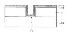
Translated fromKorean도 1a 및 도 1b는 본 발명에 따른 반도체 소자의 금속배선 형성방법을 설명하기 위한 제조공정도.1A and 1B are manufacturing process diagrams for explaining a metal wiring forming method of a semiconductor device according to the present invention.
* 도면의 주요 부분에 대한 부호설명 ** Explanation of Signs of Major Parts of Drawings *
10 : 실리콘 기판10: silicon substrate
11 : 층간절연막11: interlayer insulating film
12 : 콘택홀12: contact hole
13 : 배리어 금속막13: barrier metal film
14 : 금속배선 박막14 metal thin film
15 : 텅스텐막15: tungsten film
본 발명은 반도체 소자의 금속배선 형성방법에 관한 것으로, 보다 구체적으로는, 미세 홀 패턴의 매립특성을 확보할 수 있는 반도체 소자의 금속배선 형성방법에 관한 것이다.BACKGROUND OF THE INVENTION 1. Field of the Invention The present invention relates to a method for forming metal wiring of a semiconductor device, and more particularly, to a method for forming metal wiring of a semiconductor device capable of securing a buried characteristic of a fine hole pattern.
일반적으로, 반도체 기판과 배선 사이, 또는, 상·하층 배선 사이를 전기적으로 연결하기 위한 접속 통로로서 콘택홀을 형성하고 있으며, 이러한 콘택홀을 매립하기 위한 금속 배선의 재료로는 전도도가 높고, 경제성이 있는 텅스텐막이 주로 이용되고 있다.In general, a contact hole is formed as a connection passage for electrically connecting the semiconductor substrate and the wiring or between the upper and lower layer wirings, and as the material of the metal wiring for filling the contact hole, the conductivity is high and economical This tungsten film is mainly used.
그러나, 콘택홀의 크기가 감소함에 따라, 종래의 일반적인 CVD 방법으로는 콘택홀 내에 텅스텐막을 완전히 매립시키지 못하기 때문에, 콘택 내부의 불연속적 증착은 최종 텅스텐 증착 공정 후 콘택 내부에 동공(void)이 형성되어 금속 배선 신뢰성에 악영향을 주게 된다.However, as the size of the contact hole decreases, the conventional CVD method does not completely fill the tungsten film in the contact hole, so discontinuous deposition inside the contact forms voids in the contact after the final tungsten deposition process. This adversely affects the metal wiring reliability.
따라서, 상기한 문제점을 해결하기 위한 본 발명의 목적은, 콘택홀내의 텅스텐 매립특성을 개선시킬 수 있는 반도체 소자의 금속배선 형성방법을 제공하는 것이다.Accordingly, an object of the present invention for solving the above problems is to provide a method for forming a metal wiring of a semiconductor device that can improve the tungsten buried characteristics in the contact hole.
상기와 같은 목적을 달성하기 위한 본 발명에 따른 반도체 소자의 금속배선 형성방법은, 층간절연막을 구비하는 실리콘 기판을 제공하는 단계; 상기 층간절연막상에 콘택홀을 형성하여 상기 실리콘 기판의 활성영역을 노출시키는 단계; 상기 콘택홀이 형성된 전체구조 상면에 배리어 금속막을 증착하는 단계; 상기 배리어 금속막 상부에 ALD(Atomic Layer Deposition)방식을 적용하여 금속배선 박막을 증착하는 단계; 및 상기 금속배선 박막이 형성된 전체구조 상면에 상기 콘택홀을 매립하도록 텅스텐막을 형성하는 단계;를 포함하는 것을 특징으로 한다.Method of forming a metal wiring of a semiconductor device according to the present invention for achieving the above object comprises the steps of providing a silicon substrate having an interlayer insulating film; Forming a contact hole on the interlayer insulating film to expose an active region of the silicon substrate; Depositing a barrier metal film on an upper surface of the entire structure in which the contact hole is formed; Depositing a metallization thin film by applying an atomic layer deposition (ALD) method on the barrier metal film; And forming a tungsten film to fill the contact hole in the upper surface of the entire structure on which the metal wiring thin film is formed.
이하, 본 발명의 바람직한 실시예를 첨부한 도면에 의거하여 상세히 설명한다.Hereinafter, preferred embodiments of the present invention will be described in detail with reference to the accompanying drawings.
도 1a 및 도 1b는 본 발명에 따른 반도체 소자의 금속배선 형성방법을 설명하기 위한 제조공정도이다.1A and 1B are manufacturing process diagrams for explaining a method for forming metal wirings of a semiconductor device according to the present invention.
먼저, 도 1a에 도시된 바와같이, 층간절연막(11)이 구비된 실리콘 기판(10)을 제공한다. 그 다음, 상기 층간절연막(11)상에 실리콘 기판(10)의 활성영역을 노출시키는 콘택홀(12)을 형성한다.First, as shown in FIG. 1A, a
그 다음, 상기 콘택홀(12)이 형성된 전체구조 상면에 상기 실리콘 기판(10)과 후속 형성될 금속배선과의 전자이동 및 스트레스를 방지하기 위하여 배리어 금속막(13)을 증착한다. 이 때, 상기 배리어 금속막(13)은 바람직하게 Ti/TiN막을 사용한다.Next, a
이어서, 상기 배리어 금속막(13) 상부에 ALD(Atomic Layer Deposition)방식을 적용하여 금속배선 박막(14)을 증착한다. 이 때, 상기 금속배선 박막(14)은 바람직하게 텅스텐 박막으로 형성한다.Subsequently, an ALD (Atomic Layer Deposition) method is applied on the
상기 ALD 방식을 적용한 금속배선 박막 증착은 반응기체 SiH4와 WF6를 이용하는데, 공정순서는 다음과 같다.The metallization thin film deposition using the ALD method uses the reactant SiH4 and WF6, the process sequence is as follows.
상기 금속배선 박막(14) 증착은 챔버내에 SiH4 가스를 유입하여 상기 콘택홀이 형성된 후의 결과물 표면상에 상기 가스를 물리흡착시킨다. 그 다음, 상기 챔버내에 불활성 기체를 주입하여 퍼지(purge)를 수행하고, 상기 퍼지된 동일 챔버내에 상기 흡착된 SiH4와 WF6 가스를 반응시킴으로써 텅스텐 박막을 형성시킨다.The deposition of the metallization
이러한 ALD 공정을 반복 진행하여 원하는 텅스텐 박막의 두께를 형성할 수 있다.This ALD process may be repeated to form a desired thickness of the tungsten thin film.
그 다음, 도 1b에 도시된 바와같이, 상기 금속배선 박막(14)을 형성한 후 전체구조 상면에 콘택홀을 매립하도록 금속배선막으로서 텅스텐막(15)을 형성한다. 상기 텅스텐막(15)은 WF6 가스와 환원가스를 동시에 챔버내로 유입하여 반응시킴으로써 형성된다. 여기서, 상기 환원가스는 SiH4 또는 H2 가스를 사용한다.Then, as shown in FIG. 1B, after forming the metal interconnect
상기한 바와같은 본 발명에 따른 반도체 소자의 금속배선 형성방법은 다음과 같은 효과가 있다.The metal wiring forming method of the semiconductor device according to the present invention as described above has the following effects.
본 발명은 ALD(Atomic Layer Deposition) 방식을 적용하여 금속배선으로 사용되는 텅스텐막을 콘택홀 상에 먼저 박막화하여 형성한 다음, 상기 텅스텐 박막이 형성된 콘택홀상에 텅스텐막을 매립함으로써 반도체 소자의 금속배선을 형성한다.The present invention forms a tungsten film, which is used as a metal wiring, by first thinning it in a contact hole by applying an ALD (Atomic Layer Deposition) method, and then forms a metal wiring of a semiconductor device by embedding a tungsten film in the contact hole where the tungsten thin film is formed. do.
이에, 상기 콘택홀내의 텅스텐 매립특성을 개선함으로써 콘택 저항과 같은 전기적 특성을 향상시킬 수 있다.Thus, by improving the tungsten buried characteristics in the contact hole, it is possible to improve electrical characteristics such as contact resistance.
또한, ALD 적용으로 텅스텐 박막의 표면 거칠기(Roughness)를 개선하여 후속 패터닝 공정시 형성되는 텅스텐 라인의 선폭을 고르게 할 수 있다.In addition, the application of ALD can improve the surface roughness of the tungsten thin film to even out the line width of the tungsten line formed during the subsequent patterning process.
이 결과로써, 0.10㎛이하의 디자인 룰(Design Rule)을 갖는 기억소자에서 텅스텐 비트라인 패터닝 공정을 안정화시키고, 생산 수율 향상이 기대된다.As a result, the tungsten bit line patterning process is stabilized in a memory device having a design rule of 0.10 µm or less, and production yield is expected to be improved.
기타, 본 발명의 요지를 벗어나지 않는 범위내에서 다양하게 변경하여 실시 할 수 있다.In addition, various changes can be made without departing from the spirit of the invention.
Claims (8)
Translated fromKoreanPriority Applications (1)
| Application Number | Priority Date | Filing Date | Title |
|---|---|---|---|
| KR1020000084171AKR100680940B1 (en) | 2000-12-28 | 2000-12-28 | Metal wiring formation method of semiconductor device |
Applications Claiming Priority (1)
| Application Number | Priority Date | Filing Date | Title |
|---|---|---|---|
| KR1020000084171AKR100680940B1 (en) | 2000-12-28 | 2000-12-28 | Metal wiring formation method of semiconductor device |
Publications (2)
| Publication Number | Publication Date |
|---|---|
| KR20020054906A KR20020054906A (en) | 2002-07-08 |
| KR100680940B1true KR100680940B1 (en) | 2007-02-08 |
Family
ID=27687638
Family Applications (1)
| Application Number | Title | Priority Date | Filing Date |
|---|---|---|---|
| KR1020000084171AExpired - Fee RelatedKR100680940B1 (en) | 2000-12-28 | 2000-12-28 | Metal wiring formation method of semiconductor device |
Country Status (1)
| Country | Link |
|---|---|
| KR (1) | KR100680940B1 (en) |
Families Citing this family (2)
| Publication number | Priority date | Publication date | Assignee | Title |
|---|---|---|---|---|
| KR100873017B1 (en)* | 2002-07-19 | 2008-12-09 | 주식회사 하이닉스반도체 | Formation method of multilayer metal wiring |
| KR100866669B1 (en)* | 2006-12-27 | 2008-11-04 | 동부일렉트로닉스 주식회사 | Semiconductor Device Formation Method Using Tungsten Film |
Citations (3)
| Publication number | Priority date | Publication date | Assignee | Title |
|---|---|---|---|---|
| KR20000020013A (en)* | 1998-09-17 | 2000-04-15 | 윤종용 | Method for manufacturing semiconductor device forming metal wiring layer using interface control layer |
| KR20010059541A (en)* | 1999-12-30 | 2001-07-06 | 박종섭 | Method for forming metal line of semiconductor device |
| KR20020010821A (en)* | 2000-07-31 | 2002-02-06 | 박종섭 | Method for forming tungsten layer by using selective ALD method |
- 2000
- 2000-12-28KRKR1020000084171Apatent/KR100680940B1/ennot_activeExpired - Fee Related
Patent Citations (3)
| Publication number | Priority date | Publication date | Assignee | Title |
|---|---|---|---|---|
| KR20000020013A (en)* | 1998-09-17 | 2000-04-15 | 윤종용 | Method for manufacturing semiconductor device forming metal wiring layer using interface control layer |
| KR20010059541A (en)* | 1999-12-30 | 2001-07-06 | 박종섭 | Method for forming metal line of semiconductor device |
| KR20020010821A (en)* | 2000-07-31 | 2002-02-06 | 박종섭 | Method for forming tungsten layer by using selective ALD method |
Non-Patent Citations (1)
| Title |
|---|
| 1020000020013 * |
Also Published As
| Publication number | Publication date |
|---|---|
| KR20020054906A (en) | 2002-07-08 |
Similar Documents
| Publication | Publication Date | Title |
|---|---|---|
| KR100287180B1 (en) | Method for manufacturing semiconductor device including metal interconnection formed using interface control layer | |
| KR100719177B1 (en) | Tungsten Film Formation Method Using Selective Atomic Layer Deposition | |
| KR100215846B1 (en) | Wiring Formation Method of Semiconductor Device | |
| KR100220935B1 (en) | Metal contact formation method | |
| KR20050011479A (en) | Method for Forming Tungsten Contact Plug of Semiconductor Device | |
| US8008774B2 (en) | Multi-layer metal wiring of semiconductor device preventing mutual metal diffusion between metal wirings and method for forming the same | |
| KR100528069B1 (en) | Semiconductor Device And Method For Manufacturing The Same | |
| KR20050046056A (en) | Method of forming a metal wiring in a semiconductor device | |
| KR100680940B1 (en) | Metal wiring formation method of semiconductor device | |
| KR100578221B1 (en) | Method for manufacturing semiconductor device having diffusion barrier | |
| US7022601B2 (en) | Method of manufacturing a semiconductor device | |
| KR100551073B1 (en) | Thin Film Formation Method Using Pulsed Chemical Vapor Deposition | |
| KR0161889B1 (en) | Formation method of wiring in semiconductor device | |
| JP3070577B2 (en) | Method for manufacturing semiconductor device | |
| KR100967130B1 (en) | Metal wiring of semiconductor device and forming method thereof | |
| KR100477813B1 (en) | Tungsten Metal Wiring Formation Method of Semiconductor Device | |
| KR100499401B1 (en) | Method for forming metal interconnection layer of semiconductor device | |
| KR100780689B1 (en) | Manufacturing method of semiconductor device | |
| KR100571387B1 (en) | Copper wiring manufacturing method of semiconductor device | |
| KR20090074512A (en) | Metal wiring of semiconductor device and method of forming the same | |
| KR20020056293A (en) | Method for forming metal line in semiconductor device | |
| KR100739244B1 (en) | Manufacturing Method of Semiconductor Device | |
| KR101096444B1 (en) | Metal wiring formation method of semiconductor device | |
| KR0168162B1 (en) | Metal wiring formation method of semiconductor device | |
| KR100687876B1 (en) | Metal contact formation method of semiconductor device |
Legal Events
| Date | Code | Title | Description |
|---|---|---|---|
| PA0109 | Patent application | St.27 status event code:A-0-1-A10-A12-nap-PA0109 | |
| PN2301 | Change of applicant | St.27 status event code:A-3-3-R10-R13-asn-PN2301 St.27 status event code:A-3-3-R10-R11-asn-PN2301 | |
| PG1501 | Laying open of application | St.27 status event code:A-1-1-Q10-Q12-nap-PG1501 | |
| A201 | Request for examination | ||
| PA0201 | Request for examination | St.27 status event code:A-1-2-D10-D11-exm-PA0201 | |
| D13-X000 | Search requested | St.27 status event code:A-1-2-D10-D13-srh-X000 | |
| D14-X000 | Search report completed | St.27 status event code:A-1-2-D10-D14-srh-X000 | |
| E902 | Notification of reason for refusal | ||
| PE0902 | Notice of grounds for rejection | St.27 status event code:A-1-2-D10-D21-exm-PE0902 | |
| E13-X000 | Pre-grant limitation requested | St.27 status event code:A-2-3-E10-E13-lim-X000 | |
| P11-X000 | Amendment of application requested | St.27 status event code:A-2-2-P10-P11-nap-X000 | |
| P13-X000 | Application amended | St.27 status event code:A-2-2-P10-P13-nap-X000 | |
| E701 | Decision to grant or registration of patent right | ||
| PE0701 | Decision of registration | St.27 status event code:A-1-2-D10-D22-exm-PE0701 | |
| GRNT | Written decision to grant | ||
| PR0701 | Registration of establishment | St.27 status event code:A-2-4-F10-F11-exm-PR0701 | |
| PR1002 | Payment of registration fee | St.27 status event code:A-2-2-U10-U11-oth-PR1002 Fee payment year number:1 | |
| PG1601 | Publication of registration | St.27 status event code:A-4-4-Q10-Q13-nap-PG1601 | |
| PR1001 | Payment of annual fee | St.27 status event code:A-4-4-U10-U11-oth-PR1001 Fee payment year number:4 | |
| FPAY | Annual fee payment | Payment date:20110126 Year of fee payment:5 | |
| PR1001 | Payment of annual fee | St.27 status event code:A-4-4-U10-U11-oth-PR1001 Fee payment year number:5 | |
| LAPS | Lapse due to unpaid annual fee | ||
| PC1903 | Unpaid annual fee | St.27 status event code:A-4-4-U10-U13-oth-PC1903 Not in force date:20120203 Payment event data comment text:Termination Category : DEFAULT_OF_REGISTRATION_FEE | |
| PN2301 | Change of applicant | St.27 status event code:A-5-5-R10-R13-asn-PN2301 St.27 status event code:A-5-5-R10-R11-asn-PN2301 | |
| PN2301 | Change of applicant | St.27 status event code:A-5-5-R10-R13-asn-PN2301 St.27 status event code:A-5-5-R10-R11-asn-PN2301 | |
| PC1903 | Unpaid annual fee | St.27 status event code:N-4-6-H10-H13-oth-PC1903 Ip right cessation event data comment text:Termination Category : DEFAULT_OF_REGISTRATION_FEE Not in force date:20120203 | |
| PN2301 | Change of applicant | St.27 status event code:A-5-5-R10-R13-asn-PN2301 St.27 status event code:A-5-5-R10-R11-asn-PN2301 | |
| P22-X000 | Classification modified | St.27 status event code:A-4-4-P10-P22-nap-X000 |