KR100674950B1 - Semiconductor substrate with reference semiconductor chip and semiconductor chip assembly method using same - Google Patents
Semiconductor substrate with reference semiconductor chip and semiconductor chip assembly method using sameDownload PDFInfo
- Publication number
- KR100674950B1 KR100674950B1KR1020050006102AKR20050006102AKR100674950B1KR 100674950 B1KR100674950 B1KR 100674950B1KR 1020050006102 AKR1020050006102 AKR 1020050006102AKR 20050006102 AKR20050006102 AKR 20050006102AKR 100674950 B1KR100674950 B1KR 100674950B1
- Authority
- KR
- South Korea
- Prior art keywords
- semiconductor chip
- semiconductor
- semiconductor chips
- chips
- semiconductor substrate
- Prior art date
- Legal status (The legal status is an assumption and is not a legal conclusion. Google has not performed a legal analysis and makes no representation as to the accuracy of the status listed.)
- Expired - Fee Related
Links
Images


Classifications
- B—PERFORMING OPERATIONS; TRANSPORTING
- B32—LAYERED PRODUCTS
- B32B—LAYERED PRODUCTS, i.e. PRODUCTS BUILT-UP OF STRATA OF FLAT OR NON-FLAT, e.g. CELLULAR OR HONEYCOMB, FORM
- B32B7/00—Layered products characterised by the relation between layers; Layered products characterised by the relative orientation of features between layers, or by the relative values of a measurable parameter between layers, i.e. products comprising layers having different physical, chemical or physicochemical properties; Layered products characterised by the interconnection of layers
- B32B7/02—Physical, chemical or physicochemical properties
- H—ELECTRICITY
- H01—ELECTRIC ELEMENTS
- H01L—SEMICONDUCTOR DEVICES NOT COVERED BY CLASS H10
- H01L23/00—Details of semiconductor or other solid state devices
- H01L23/544—Marks applied to semiconductor devices or parts, e.g. registration marks, alignment structures, wafer maps
- A—HUMAN NECESSITIES
- A47—FURNITURE; DOMESTIC ARTICLES OR APPLIANCES; COFFEE MILLS; SPICE MILLS; SUCTION CLEANERS IN GENERAL
- A47F—SPECIAL FURNITURE, FITTINGS, OR ACCESSORIES FOR SHOPS, STOREHOUSES, BARS, RESTAURANTS OR THE LIKE; PAYING COUNTERS
- A47F13/00—Shop or like accessories
- B—PERFORMING OPERATIONS; TRANSPORTING
- B32—LAYERED PRODUCTS
- B32B—LAYERED PRODUCTS, i.e. PRODUCTS BUILT-UP OF STRATA OF FLAT OR NON-FLAT, e.g. CELLULAR OR HONEYCOMB, FORM
- B32B15/00—Layered products comprising a layer of metal
- B32B15/04—Layered products comprising a layer of metal comprising metal as the main or only constituent of a layer, which is next to another layer of the same or of a different material
- B32B15/046—Layered products comprising a layer of metal comprising metal as the main or only constituent of a layer, which is next to another layer of the same or of a different material of foam
- B—PERFORMING OPERATIONS; TRANSPORTING
- B32—LAYERED PRODUCTS
- B32B—LAYERED PRODUCTS, i.e. PRODUCTS BUILT-UP OF STRATA OF FLAT OR NON-FLAT, e.g. CELLULAR OR HONEYCOMB, FORM
- B32B15/00—Layered products comprising a layer of metal
- B32B15/18—Layered products comprising a layer of metal comprising iron or steel
- B—PERFORMING OPERATIONS; TRANSPORTING
- B32—LAYERED PRODUCTS
- B32B—LAYERED PRODUCTS, i.e. PRODUCTS BUILT-UP OF STRATA OF FLAT OR NON-FLAT, e.g. CELLULAR OR HONEYCOMB, FORM
- B32B15/00—Layered products comprising a layer of metal
- B32B15/20—Layered products comprising a layer of metal comprising aluminium or copper
- B—PERFORMING OPERATIONS; TRANSPORTING
- B32—LAYERED PRODUCTS
- B32B—LAYERED PRODUCTS, i.e. PRODUCTS BUILT-UP OF STRATA OF FLAT OR NON-FLAT, e.g. CELLULAR OR HONEYCOMB, FORM
- B32B25/00—Layered products comprising a layer of natural or synthetic rubber
- B32B25/04—Layered products comprising a layer of natural or synthetic rubber comprising rubber as the main or only constituent of a layer, which is next to another layer of the same or of a different material
- B32B25/045—Layered products comprising a layer of natural or synthetic rubber comprising rubber as the main or only constituent of a layer, which is next to another layer of the same or of a different material of foam
- B—PERFORMING OPERATIONS; TRANSPORTING
- B32—LAYERED PRODUCTS
- B32B—LAYERED PRODUCTS, i.e. PRODUCTS BUILT-UP OF STRATA OF FLAT OR NON-FLAT, e.g. CELLULAR OR HONEYCOMB, FORM
- B32B27/00—Layered products comprising a layer of synthetic resin
- B32B27/06—Layered products comprising a layer of synthetic resin as the main or only constituent of a layer, which is next to another layer of the same or of a different material
- B32B27/065—Layered products comprising a layer of synthetic resin as the main or only constituent of a layer, which is next to another layer of the same or of a different material of foam
- B—PERFORMING OPERATIONS; TRANSPORTING
- B32—LAYERED PRODUCTS
- B32B—LAYERED PRODUCTS, i.e. PRODUCTS BUILT-UP OF STRATA OF FLAT OR NON-FLAT, e.g. CELLULAR OR HONEYCOMB, FORM
- B32B27/00—Layered products comprising a layer of synthetic resin
- B32B27/30—Layered products comprising a layer of synthetic resin comprising vinyl (co)polymers; comprising acrylic (co)polymers
- B32B27/304—Layered products comprising a layer of synthetic resin comprising vinyl (co)polymers; comprising acrylic (co)polymers comprising vinyl halide (co)polymers, e.g. PVC, PVDC, PVF, PVDF
- B—PERFORMING OPERATIONS; TRANSPORTING
- B32—LAYERED PRODUCTS
- B32B—LAYERED PRODUCTS, i.e. PRODUCTS BUILT-UP OF STRATA OF FLAT OR NON-FLAT, e.g. CELLULAR OR HONEYCOMB, FORM
- B32B27/00—Layered products comprising a layer of synthetic resin
- B32B27/32—Layered products comprising a layer of synthetic resin comprising polyolefins
- B—PERFORMING OPERATIONS; TRANSPORTING
- B32—LAYERED PRODUCTS
- B32B—LAYERED PRODUCTS, i.e. PRODUCTS BUILT-UP OF STRATA OF FLAT OR NON-FLAT, e.g. CELLULAR OR HONEYCOMB, FORM
- B32B27/00—Layered products comprising a layer of synthetic resin
- B32B27/36—Layered products comprising a layer of synthetic resin comprising polyesters
- B32B27/365—Layered products comprising a layer of synthetic resin comprising polyesters comprising polycarbonates
- B—PERFORMING OPERATIONS; TRANSPORTING
- B32—LAYERED PRODUCTS
- B32B—LAYERED PRODUCTS, i.e. PRODUCTS BUILT-UP OF STRATA OF FLAT OR NON-FLAT, e.g. CELLULAR OR HONEYCOMB, FORM
- B32B5/00—Layered products characterised by the non- homogeneity or physical structure, i.e. comprising a fibrous, filamentary, particulate or foam layer; Layered products characterised by having a layer differing constitutionally or physically in different parts
- B32B5/18—Layered products characterised by the non- homogeneity or physical structure, i.e. comprising a fibrous, filamentary, particulate or foam layer; Layered products characterised by having a layer differing constitutionally or physically in different parts characterised by features of a layer of foamed material
- B32B5/20—Layered products characterised by the non- homogeneity or physical structure, i.e. comprising a fibrous, filamentary, particulate or foam layer; Layered products characterised by having a layer differing constitutionally or physically in different parts characterised by features of a layer of foamed material foamed in situ
- G—PHYSICS
- G09—EDUCATION; CRYPTOGRAPHY; DISPLAY; ADVERTISING; SEALS
- G09F—DISPLAYING; ADVERTISING; SIGNS; LABELS OR NAME-PLATES; SEALS
- G09F23/00—Advertising on or in specific articles, e.g. ashtrays, letter-boxes
- G09F23/06—Advertising on or in specific articles, e.g. ashtrays, letter-boxes the advertising matter being combined with articles for restaurants, shops or offices
- H—ELECTRICITY
- H01—ELECTRIC ELEMENTS
- H01L—SEMICONDUCTOR DEVICES NOT COVERED BY CLASS H10
- H01L2223/00—Details relating to semiconductor or other solid state devices covered by the group H01L23/00
- H01L2223/544—Marks applied to semiconductor devices or parts
- H01L2223/5442—Marks applied to semiconductor devices or parts comprising non digital, non alphanumeric information, e.g. symbols
- H—ELECTRICITY
- H01—ELECTRIC ELEMENTS
- H01L—SEMICONDUCTOR DEVICES NOT COVERED BY CLASS H10
- H01L2223/00—Details relating to semiconductor or other solid state devices covered by the group H01L23/00
- H01L2223/544—Marks applied to semiconductor devices or parts
- H01L2223/54453—Marks applied to semiconductor devices or parts for use prior to dicing
- H01L2223/54466—Located in a dummy or reference die
- H—ELECTRICITY
- H01—ELECTRIC ELEMENTS
- H01L—SEMICONDUCTOR DEVICES NOT COVERED BY CLASS H10
- H01L2223/00—Details relating to semiconductor or other solid state devices covered by the group H01L23/00
- H01L2223/544—Marks applied to semiconductor devices or parts
- H01L2223/54473—Marks applied to semiconductor devices or parts for use after dicing
- H01L2223/5448—Located on chip prior to dicing and remaining on chip after dicing
- H—ELECTRICITY
- H01—ELECTRIC ELEMENTS
- H01L—SEMICONDUCTOR DEVICES NOT COVERED BY CLASS H10
- H01L2924/00—Indexing scheme for arrangements or methods for connecting or disconnecting semiconductor or solid-state bodies as covered by H01L24/00
- H01L2924/0001—Technical content checked by a classifier
- H01L2924/0002—Not covered by any one of groups H01L24/00, H01L24/00 and H01L2224/00
- Y—GENERAL TAGGING OF NEW TECHNOLOGICAL DEVELOPMENTS; GENERAL TAGGING OF CROSS-SECTIONAL TECHNOLOGIES SPANNING OVER SEVERAL SECTIONS OF THE IPC; TECHNICAL SUBJECTS COVERED BY FORMER USPC CROSS-REFERENCE ART COLLECTIONS [XRACs] AND DIGESTS
- Y10—TECHNICAL SUBJECTS COVERED BY FORMER USPC
- Y10S—TECHNICAL SUBJECTS COVERED BY FORMER USPC CROSS-REFERENCE ART COLLECTIONS [XRACs] AND DIGESTS
- Y10S438/00—Semiconductor device manufacturing: process
- Y10S438/975—Substrate or mask aligning feature
Landscapes
- Physics & Mathematics (AREA)
- General Physics & Mathematics (AREA)
- Engineering & Computer Science (AREA)
- Condensed Matter Physics & Semiconductors (AREA)
- Computer Hardware Design (AREA)
- Microelectronics & Electronic Packaging (AREA)
- Power Engineering (AREA)
- Theoretical Computer Science (AREA)
- Testing Or Measuring Of Semiconductors Or The Like (AREA)
Abstract
Translated fromKoreanDescription
Translated fromKorean도 1은 복수의 반도체 칩들을 포함하는 종래 반도체 기판을 보여주는 평면도이다.1 is a plan view illustrating a conventional semiconductor substrate including a plurality of semiconductor chips.
도 2는 반도체 칩에 대한 종래 잉크 표시 방법을 보여주는 단면도이다.2 is a cross-sectional view showing a conventional ink display method for a semiconductor chip.
도 3은 기준 반도체 칩을 구비하는 본 발명의 실시예에 따른 반도체 기판을 보여주는 평면도이다.3 is a plan view illustrating a semiconductor substrate in accordance with an embodiment of the present invention having a reference semiconductor chip.
도 4는 본 발명의 일 실시예에 따른 기준 반도체 칩을 보여주는 평면도이다.4 is a plan view illustrating a reference semiconductor chip according to an embodiment of the present invention.
도 5는 도 4의 기준 반도체 칩의 I-I'에 따른 단면도이다.5 is a cross-sectional view taken along line II ′ of the reference semiconductor chip of FIG. 4.
도 6은 본 발명의 다른 실시예에 따른 기준 반도체 칩을 보여주는 평면도이다.6 is a plan view illustrating a reference semiconductor chip according to another embodiment of the present invention.
도 7은 도 6의 기준 반도체 칩의 II-II'에 따른 단면도이다.FIG. 7 is a cross-sectional view taken along line II-II ′ of the reference semiconductor chip of FIG. 6.
도 8은 본 발명의 실시예에 따른 반도체 칩 어셈블리 방법을 보여주는 순서도이다.8 is a flowchart illustrating a semiconductor chip assembly method according to an embodiment of the present invention.
도 9는 본 발명의 실시예에 따른 기준 반도체 칩 식별 표시 방법을 보여주는 단면도이다.9 is a cross-sectional view illustrating a reference semiconductor chip identification display method according to an embodiment of the present invention.
도 10은 본 발명의 실시예에 따른 잉크 표시 방법을 보여주는 평면도이다.10 is a plan view showing an ink display method according to an embodiment of the present invention.
본 발명은 반도체 칩 어셈블리 방법에 관한 것으로서, 특히 복수의 반도체 칩을 포함하는 반도체 기판에 대한 전기적인 다이 소팅 시험 및 각 반도체 칩들에 대한 물리적인 분리 단계를 포함하는 반도체 칩 어셈블리 방법에 관한 것이다.The present invention relates to a semiconductor chip assembly method, and more particularly, to a semiconductor chip assembly method including an electrical die sorting test for a semiconductor substrate including a plurality of semiconductor chips and a physical separation step for each semiconductor chip.
반도체 칩들은 반도체 기판, 예를 들어 실리콘 기판에 매트릭스 형태로 동시에 여러 개가 제조되는 것이 일반적이다. 매트릭스로 구분되는 각 반도체 칩을 갖는 반도체 기판 부분을 하나의 다이(die)라고 부르기도 한다. 반도체 기판 상에 반도체 칩들에 대한 제조 공정 단계가 완료되면, 이어서 반도체 기판의 각 반도체 칩에 대해 전기적 시험을 거쳐 불량 반도체 칩을 분리해 내는 단계가 이어진다.It is common to manufacture several semiconductor chips simultaneously in a matrix form on a semiconductor substrate, for example, a silicon substrate. A portion of a semiconductor substrate having each semiconductor chip separated by a matrix is also called a die. After the manufacturing process steps for the semiconductor chips on the semiconductor substrate are completed, each semiconductor chip of the semiconductor substrate is subsequently subjected to an electrical test to isolate the defective semiconductor chip.
이러한 전기적 시험을 불량 다이를 분리해 낸다는 의미에서 전기적 다이 소팅(electrical die sorting; EDS) 시험이라고 한다. 이러한 EDS 시험 단계 후, 반도체 칩들에 대해서 어셈블리(assembly) 단계가 진행된다.This electrical test is referred to as electrical die sorting (EDS) test in the sense of removing a defective die. After this EDS test step, an assembly step is performed on the semiconductor chips.
이하 도면을 참조하여 종래 EDS 시험 및 어셈블리 단계에서 문제점에 대해서 설명한다. 도 1을 참조하면, 매트릭스 상으로 배열된 반도체 칩들(예를 들어, 10, 20, 30 등)을 포함하는 반도체 기판(100)이 도시되어 있다.With reference to the drawings will be described the problem in the conventional EDS test and assembly step. Referring to FIG. 1, a
반도체 기판(100)에 형성된 반도체 칩들(10, 20, 30 등) 중 일부는 EDS 시험에서 제외된다. 예를 들어, 반도체 기판(100)에서 가상 표시선(105) 내부의 반도체 칩들(20, 30 등) 만이 EDS 시험 대상이 되고, 표시선(105) 외부의 반도체 칩들(10 등)은 EDS 시험에서 제외된다. 반도체 기판(100) 외곽의 반도체 칩들은 패터닝이 완벽하지 않거나, 각 제조 장치에서 공정 마진을 벗어나는 부분에 해당하기 때문에, 처음부터 불량 처리하는 것이다. 여기에서 가상 표시선(105)은 실제 반도체 기판에는 표시되지 않는다.Some of the
따라서, 반도체 기판(100)에 대해 EDS 시험 또는 어셈블리 단계를 진행할 때, 첫 번째 진행할 반도체 칩 또는 다이(예를 들어, 20)를 작업자가 외관상으로 구분해 내는데 어려움이 있다. 반도체 기판(100)이 EDS 시험 또는 어셈블리 장치에 로딩되면, 먼저 첫 번째 반도체 칩 또는 다이(20)를 기준으로 정렬 및 작업이 진행된다.Therefore, when the EDS test or assembly step is performed on the
하지만, 첫 번째 반도체 칩(20) 주변에도 여려 반도체 칩들(10, 30 등)이 있기 때문에 첫 번째 반도체 칩(20)에 대한 식별 표시가 필요하다. 도 2를 참조하면, 작업자들이 종래 잉크를 이용하여 첫 번째 반도체 칩 또는 다이를 표시하는 방법이 도시되어 있다. 이러한 잉크 표시는 첫 번째 반도체 칩에 대한 표시의 용도보다는 EDS 시험 후 불량 반도체 칩들에 대한 표시로 많이 이용된다.However, since there are
잉크(ink, 70)는 실리콘 웨이퍼(50) 상의 패시베이션층(passivation layer, 550)을 덮고 있는 폴리이미드층(polyimide layer, 60) 상에 위치된다. 실리콘 웨이퍼는 약 675 um 두께이며 폴리이미드층은 약 4 um 두께일 때, 잉크는 약 25um 두께에 이른다. 따라서, 작업자가 첫 번째 반도체 칩(도 1의 20)과 그 주변의 반도체 칩들(10, 30 등)을 구분하기가 어려워, 잉크 에러가 발생할 확률이 높다.Ink 70 is located on
더구나, 최근에는 EDS 시험 후 어셈블리 진행 시 잉크 표시를 하지 않고 어셈블리를 진행하는 제품도 있다. 이러한 잉크 표시가 없는 반도체 기판의 경우에는, 반도체 칩 또는 다이의 좌표 데이터를 가지고서 어셈블리를 진행하고 있다. 이에 따라, 첫 번째 반도체 칩 또는 다이의 좌표가 매우 중요하다. 특히, 백랩(back-lap) 두께가 감소하고, 파운드리(foundry) 사업으로 인하여 대부분의 제품이 잉크 표시가 없이 진행되는 경향이 늘고 있다.In addition, recently, some products do not display the ink when the assembly is performed after the EDS test. In the case of a semiconductor substrate without such an ink mark, the assembly is performed with the coordinate data of the semiconductor chip or the die. Accordingly, the coordinates of the first semiconductor chip or die are very important. In particular, the back-lap thickness is reduced, and the foundry business is increasing the tendency of most products to go without ink marks.
따라서, 반도체 칩들에 대한 EDS 시험 및 어셈블리 단계에서 첫 번째 반도체 칩 또는 다이의 구분이 매우 중요한 이슈로 대두되고 있다. 하지만, 현재 첫 번째 다이가 다른 다이와 외관으로 구분되지 않아 오류가 종종 발생하고 있다. 특히, 이를 명확히 하기 위해, 한도 견본을 만들어 작업지침서로 삼고 있음에도 불구하고 첫 번째 다이를 잘못 지적하는 오류가 발생하고 있다.Therefore, the distinction of the first semiconductor chip or die is an important issue in the EDS test and assembly stage for semiconductor chips. However, errors often occur because the first die is currently not distinguished from other dies. In particular, to clarify this, there is an error in incorrectly pointing to the first die despite the fact that the limit sample has been created and used as a work order.
본 발명이 이루고자 하는 기술적 과제는 기준 반도체 칩을 참고로 한 반도체 칩 어셈블리 방법을 제공하는 데 있다.An object of the present invention is to provide a method for assembling a semiconductor chip with reference to a reference semiconductor chip.
본 발명이 이루고자 하는 다른 기술적 과제는 기준 반도체 칩이 표시된 반도체 기판을 제공하는 데 있다.Another object of the present invention is to provide a semiconductor substrate on which a reference semiconductor chip is displayed.
상기 기술적 과제를 달성하기 위한 본 발명의 일 태양에 따르면, 복수의 반도체 칩들이 형성된 반도체 기판을 제공하는 단계; 상기 반도체 칩들 가운데, 하나의 기준 반도체 칩(reference semiconductor chip)에 식별 표시를 하는 단계; 및 상기 기준 반도체 칩을 참고하여 상기 반도체 기판을 정렬하여, 상기 반도체 기판의 상기 반도체 칩들에 대해서 전기적인 다이 소팅(EDS) 시험을 수행하는 단계를 포함하는 반도체 칩 어셈블리 방법이 제공된다.According to an aspect of the present invention for achieving the above technical problem, providing a semiconductor substrate having a plurality of semiconductor chips formed; Marking an identification mark on one reference semiconductor chip among the semiconductor chips; And arranging the semiconductor substrate with reference to the reference semiconductor chip, and performing an electrical die sorting (EDS) test on the semiconductor chips of the semiconductor substrate.
또한, 본 발명에 따른 바람직한 실시예에 있어서, 상기 식별 표시 단계는 상기 기준 반도체 칩 상에 레이저(laser)를 조사하여 수행하는 것이 바람직하다. 나아가, 상기 레이저 조사 단계는 상기 기준 반도체 칩의 크기에 맞추어 초점 크기를 조정하는 것이 더욱 바람직하다. 또는, 상기 레이저 조사 단계는 상기 기준 반도체 칩의 표면을 변형시켜 수행할 수 있다.In addition, in a preferred embodiment of the present invention, the identification display step is preferably performed by irradiating a laser on the reference semiconductor chip. Further, in the laser irradiation step, it is more preferable to adjust the focal size according to the size of the reference semiconductor chip. Alternatively, the laser irradiation step may be performed by modifying the surface of the reference semiconductor chip.
또한, 상기 식별 단계는 상기 기준 반도체 칩 상에 식별용 레이저 마킹(laser marking)을 하여 수행할 수도 있다.In addition, the identification step may be performed by laser marking for identification on the reference semiconductor chip.
또한, 상기 전기적인 다이 소팅 시험(EDS) 단계는 시험 결과를 상기 기준 반도체 칩을 참고로 한 상기 반도체 칩들의 좌표와 함께 저장하는 것이 바람직하다.Further, the electrical die sorting test (EDS) step preferably stores the test results together with the coordinates of the semiconductor chips with reference to the reference semiconductor chip.
또한, 상기 전기적인 다이 소팅(EDS) 시험 단계 후, 상기 시험 결과에 따라서 상기 반도체 칩들을 물리적으로 분리하는 단계를 더 포함할 수 있다. 상기 분리 단계는 상기 기준 반도체 칩을 참고하여 상기 반도체 기판을 정렬하여 수행할 수 있다. 또한, 상기 분리 단계 전에 상기 시험 결과에 따라서 상기 반도체 칩들 상에 잉크 표시를 하는 단계가 더 포함될 수도 있다. 상기 잉크 표시 단계는 상기 전기적인 다이 소팅 시험(EDS) 단계에서 저장된 상기 좌표를 이용하여 수행할 수 있다.The method may further include physically separating the semiconductor chips according to the test result after the electrical die sorting (EDS) test step. The separating may be performed by aligning the semiconductor substrate with reference to the reference semiconductor chip. Further, before the separating step, the step of marking the ink on the semiconductor chips according to the test result may be further included. The ink marking step may be performed using the coordinates stored in the electrical die sorting test (EDS) step.
또한, 상기 실시예들에 있어서, 상기 기준 반도체 칩은 상기 반도체 기판 상에서 전기적인 다이 소팅(EDS) 시험이 수행되는 첫 번째 반도체 칩인 것이 바람직 하다.Further, in the above embodiments, the reference semiconductor chip is preferably the first semiconductor chip on which the electrical die sorting (EDS) test is performed on the semiconductor substrate.
상기 기술적 과제를 달성하기 위한 본 발명의 다른 태양에 따르면, 복수의 반도체 칩들이 제조된 반도체 기판에 대해서 상기 반도체 칩들을 전기적인 특성에 따라 소팅하고 분리하여 어셈블리 하는 방법으로서, 상기 반도체 칩들을 소팅하기 전에, 상기 반도체 칩 가운데 하나의 기준 반도체 칩에 식별 표시를 하는 단계를 포함하는 반도체 칩 어셈블리 방법이 제공된다.According to another aspect of the present invention for achieving the above technical problem, a method for sorting and separating and assembling the semiconductor chips according to the electrical characteristics with respect to a semiconductor substrate fabricated a plurality of semiconductor chips, sorting the semiconductor chips Previously, there is provided a semiconductor chip assembly method comprising the step of placing an identification mark on one of the semiconductor chips.
상기 다른 기술적 과제를 달성하기 위한 본 발명의 태양에 따르면, 매트릭스 상으로 배열된 복수의 반도체 칩들을 포함하는 것으로서, 상기 반도체 칩들 가운데 하나의 기준 반도체 칩 상에는 식별 표시가 되어 있는 반도체 기판이 제공된다.According to an aspect of the present invention for achieving the above another technical problem, there is provided a semiconductor substrate comprising a plurality of semiconductor chips arranged in a matrix, the identification display on one of the reference semiconductor chips of the semiconductor chips.
상기 식별 표시는 레이저 마킹인 것이 바람직하다. 나아가, 상기 식별 표시는 상기 반도체 칩의 표면층이 열 경화된 것일 수도 있다.The identification mark is preferably laser marking. In addition, the identification mark may be a heat-cured surface layer of the semiconductor chip.
또한, 상기 식별 표시가 되어 있는 반도체 칩은 상기 반도체 칩들에 대한 어셈블리를 위한 첫 번째 반도체 칩인 것이 바람직하다.In addition, the semiconductor chip marked with the identification mark is preferably the first semiconductor chip for the assembly of the semiconductor chips.
이하, 첨부한 도면을 참조하여 본 발명에 따른 바람직한 실시예를 설명함으로써 본 발명을 상세하게 설명한다. 그러나 본 발명은 이하에서 개시되는 실시예에 한정되는 것이 아니라 서로 다른 다양한 형태로 구현될 것이며, 단지 본 실시예는 본 발명의 개시가 완전하도록 하며, 통상의 지식을 가진 자에게 발명의 범주를 완전하게 알려주기 위해 제공되는 것이다. 도면에서 구성 요소들은 설명의 편의를 위하여 그 크기가 과장되어 있다.Hereinafter, exemplary embodiments of the present invention will be described in detail with reference to the accompanying drawings. However, the present invention is not limited to the embodiments disclosed below, but will be implemented in various forms, and only the present embodiments are intended to complete the disclosure of the present invention and to those skilled in the art to fully understand the scope of the invention. It is provided to inform you. In the drawings, the components are exaggerated in size for convenience of description.
도 3은 기준 반도체 칩(220)을 구비하는 본 발명의 실시예에 따른 반도체 기 판(200)을 보여주는 평면도이다. 반도체 기판(200)에는 복수의 반도체 칩들(예를 들어, 210, 220, 230 등)이 매트릭스로 배열되어 있다. 여기에서 참조 부호는 세 개의 반도체 칩들(210, 220, 230)에 대해서만 예시적으로 표시되었다.3 is a plan view illustrating a
이러한 매트릭스 구조의 반도체 칩들(210, 220, 230 등)은 제조 공정 상의 포토리소그래피 단계와 식각 단계를 거쳐서 형성될 수 있다. 또한, 반도체 칩들(210, 220, 230 등)은 반도체 기판(200)의 매트릭스를 이룬다는 점에서 다이들(dies)이라고도 불린다.The
반도체 칩들(210, 220, 230 등)의 수는 제품, 반도체 기판(200)의 크기 및 집적도에 따라서 달라질 수 있음은 해당 기술분야에서 통상의 지식을 가진 자에게 있어서 자명하다. 즉, 도 3에서는 예시적으로 반도체 칩들(210, 220, 230 등)을 도시한 것이다. 또한, 기준 반도체 칩(220)을 제외한 다른 반도체 칩들(210, 230 등)은 특별히 다른 처리를 하지 않는 이상, 기본적으로 외관상 구분이 가지 않는다. 즉, 기준 반도체 칩(220)은 외관상 다른 반도체 칩들(210, 230 등)과 구분되어 있다.It will be apparent to those skilled in the art that the number of
도 1에서 설명된 바와 같이, 반도체 기판(200)의 반도체 칩들(210, 220, 230 등) 가운데 일부는 EDS 시험 및 어셈블리에서 처음부터 제외된다. 예를 들어, 표시선 (205) 내부의 반도체 칩들(220, 230 등)은 EDS 시험 및 어셈블리의 대상이 되지만, 표시선(205) 외부의 반도체 칩들(210 등)은 EDS 시험 및 어셈블리의 대상에서 처음부터 제외된다. 이때, 표시선(205)은 실제 반도체 기판(200)에는 표시되지 않는 편의상의 가상선(imaginary line)이다.As illustrated in FIG. 1, some of the
기준 반도체 칩(220)은 임의의 반도체 칩이 될 수도 있지만, EDS 시험의 대상이 되는 첫 번째 반도체 칩(220)이 되는 것이 바람직하다. 이에 따라, EDS 시험장치는 기준 반도체 칩(220)을 참고하여 반도체 기판(200)을 정렬할 수 있다. 또한, 기준 반도체 칩(220)을 기준으로 EDS 대상 칩들에 대한 좌표를 입력받아 EDS 시험을 진행할 수 있게 된다.The
즉, EDS 시험을 진행하는 작업자는 외관상 구분이 가는 기준 반도체 칩(220)을 기준으로 EDS 시험을 진행할 수 있어, 종래 좌표만으로 첫 번째 반도체 칩을 찾을 때에 비해서 오류를 줄일 수 있다. 나아가, 어셈블리 단계에서 잉크 작업도 기준 반도체 칩(220)을 기준으로 수행할 수 있다.That is, the operator performing the EDS test can perform the EDS test on the basis of the
또한, 잉크 표시가 생략된 어셈블리 단계에서는 EDS 시험 결과를 기준 반도체 칩(220)을 참고로 한 좌표로 직접 입력받음으로써 오류 없이 작업을 진행할 수 있게 된다.In addition, in the assembly step in which the ink marking is omitted, the EDS test result may be directly input to the coordinates with reference to the
이하 도 4 내지 도 6을 참조하여 기준 반도체 칩(도 3의 220)을 보다 상세하게 설명한다.Hereinafter, the
도 4는 본 발명의 일 실시예에 따른 기준 반도체 칩(220)을 보여주는 평면도이고, 도 5는 도 4의 기준 반도체 칩(220)의 I-I'에 따른 단면도이다.4 is a plan view illustrating a
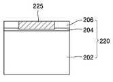
도 4를 참조하면, 기준 반도체 칩(220)의 표면에는 외관상 구분되는 식별 표시(225)가 되어 있다. 기준 반도체 칩(220)의 표면에는 폴리이미드층(polyimide layer, 206)이 형성되어 있을 수 있다. 보다 구체적으로 보면, 식별 표시(225)는 표면층, 즉 예를 들어 폴리이미드층(206)의 경화층일 수 있다.Referring to FIG. 4, an
도 5를 참조하면, 식별 표시(225)는 폴리이미드층(206) 아래의 패시베이션층(passivation layer, 204)의 일부의 경화층까지 포함할 수도 있다. 패시베이션층(204) 아래에는 반도체 칩 형성을 위한 패턴이 형성된 웨이퍼(202)가 위치되어 있다.Referring to FIG. 5, the
도 6은 본 발명의 다른 실시예에 따른 기준 반도체 칩(220)을 보여주는 평면도이고, 도 7은 도 6의 기준 반도체 칩(220)의 II-II'에 따른 단면도이다.6 is a plan view illustrating a
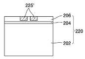
도 6 및 도 7을 참조하면, 기준 반도체 칩(220)의 표면에는 외관상 구분되는 다른 식별 표시(225')가 되어 있다. 보다 구체적으로 보면, 식별 표시(225')는 표면층, 즉 예를 들어 폴리이미드층(206)에 형성된 레이저 마킹일 수 있다. 이 때, 식별 표시(225')는 폴리이미드층(206) 내에 형성되는 것으로 도시되었지만, 패시베이션층(204)에 거쳐서 형성될 수도 있다.6 and 7, another
또한, 식별 표시(225')는 "V" 표시의 레이저 마킹으로 도시되었지만, 그 외의 다른 글자 또는 도형에도 적용될 수 있음은 해당 기술 분야에서 통상의 지식을 가진 자에게 자명하다.In addition, although the identification mark 225 'is shown as a laser marking of the "V" mark, it is apparent to those skilled in the art that it may be applied to other letters or figures.
도 8은 본 발명의 실시예에 따른 반도체 칩 어셈블리 방법(300)을 보여주는 순서도이다. 그리고, 도 9는 본 발명의 실시예에 따른 기준 반도체 칩 식별 표시 방법을 보여주는 단면도이고, 도 10은 본 발명의 실시예에 따른 잉크 표시 방법을 보여주는 평면도이다. 이하에서는 도 8의 순서도에 따라서, 도 9 및 도 10을 참조하여 어셈블리 방법(300)을 설명한다. 나아가, 어셈블리 방법(300)은 도 3 내지 도 7을 참조할 수 있다.8 is a flowchart illustrating a semiconductor
도 3을 참조하면, 먼저 복수의 반도체 칩들(210, 220, 230 등)이 형성된 반도체 기판(200)을 제공한다(도 8의 단계 310). 이어서, 상기 반도체 칩들(210, 220, 230 등) 가운데, 하나의 기준 반도체 칩(220)에 식별 표시(225)를 한다(도 8의 단계 320). 기준 반도체 칩(220)은 EDS 시험이 진행될 첫 번째 반도체 칩인 것이 바람직하다.Referring to FIG. 3, first, a
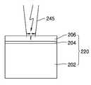
도 9를 참조하면, 식별 표시 단계(도 8의 단계 320)는 기준 반도체 칩(220) 상에 레이저(245)를 조사하여 수행하는 것이 바람직하다. 레이저(245)가 조사됨에 따라 기준 반도체 칩(220)의 표면, 예를 들어 폴리이미드층(206) 또는 폴리이미드층(206)/패시베이션층(204)이 변형되어 경화된다. 이에 따라, 도 4 및 도 5에 도시된 바와 같이, 기준 반도체 칩(220)이 다른 반도체 칩들과 외관상 구분될 수 있다.Referring to FIG. 9, the identification display step (step 320 of FIG. 8) may be performed by irradiating the
다시 도 9를 참조하면, 레이저(245)의 초점 크기(f)는 기준 반도체 칩(220)의 평면상 크기에 따라 조정될 수 있다. 즉, 레이저(245)의 조사에 의한 폴리이미드층(206)의 경화는 기준 반도체 칩(220) 내로 제한되도록 조정될 수 있다.Referring back to FIG. 9, the focal size f of the
또한, 식별 표시 단계(도 8의 단계 320)는 레이저(245) 조사를 통해 기준 반도체 칩(220)에 레이저 마킹을 하는 방법으로 수행할 수도 있다. 이에 따르면, 예를 들어, 도 6 및 도 7에 도시된 바와 같은 레이저 마킹(225')이 가능하다. 따라서, 기준 반도체 칩(220)이 다른 반도체 칩들과 외관상 역시 구분될 수 있다.In addition, the identification display step (step 320 of FIG. 8) may be performed by laser marking the
도 10을 참조하면, 이어서 기준 반도체 칩(220)을 참고로 하여 반도체 기판(200)을 정렬하여, 반도체 칩들(210, 220, 230 등)에 대해 EDS 시험을 진행한다(도 8의 단계 330).Referring to FIG. 10, the
보다 구체적으로 보면, 작업자가 기준 반도체 칩(220)을 외관으로 인식하여 반도체 기판(200)을 정렬할 수 있게 된다. 나아가, 기준 반도체 칩(220)이 정렬됨에 따라, 기준 반도체 칩(220)을 첫 번째 진행 다이로 하고, EDS 시험이 진행될 다른 반도체 칩에 대한 좌표를 지정할 수 있게 된다. 따라서, 종래 첫 번째 반도체 칩 지정 오류로 인한 EDS 시험 및 어셈블리 상의 문제가 해결될 수 있다.More specifically, the operator may recognize the
이어서, 시험 결과에 따라서 반도체 칩들 상에 잉크 표시(255)를 한다(도 8의 단계 340). 잉크 표시(255)는 EDS 시험 결과에 따른 불량 다이 여부에 대한 표시이다. 예를 들어, 불량 다이들에 대해서 잉크 표시(255)를 할 수 있다. 반대로, 정상 다이들에 대해서 잉크 표시(255)를 하는 것도 가능하다.Then, ink markings 255 are made on the semiconductor chips according to the test result (step 340 of FIG. 8). The ink mark 255 is an indication of whether or not a die is bad according to the EDS test result. For example, ink markings 255 may be made for defective dies. Conversely, it is also possible to make an ink mark 255 for normal dies.
따라서, 작업자들이 시각적으로 정상 또는 불량 다이들을 구분할 수 있다. 잉크 표시 단계(도 8의 단계 340)도 기준 반도체 칩(220)을 참고하여 반도체 기판(200)을 정렬하여 진행할 수 있다. 또는, 잉크 표시 단계(단계 340)는 EDS 시험 단계에서 저장된 좌표를 이용하여 반도체 칩들을 구분하여 수행할 수도 있다. 하지만, 제품에 따라서는 잉크 표시 단계(단계 340)가 생략될 수도 있다.Thus, workers can visually distinguish between normal or bad dies. The ink display step (step 340 of FIG. 8) may also be performed by aligning the
이어서, 시험 결과에 따라서 반도체 칩들을 물리적으로 분리한다(도 8의 단계 350). 반도체 칩들의 분리를 포함한 어셈블리 단계도 또한, 기준 반도체 칩(220)을 참고로 하여 진행할 수 있다. 특히, 제품에 잉크 표시(250)가 없는 경우에는 기준 반도체 칩(220)을 참고로 한 각 반도체 칩들의 좌표와 EDS 시험 결과를 피드백 받음으로써 정상 및 불량 반도체 칩들을 구분하여 작업을 진행할 수 있다.Subsequently, the semiconductor chips are physically separated according to the test result (step 350 of FIG. 8). The assembly step including the separation of the semiconductor chips may also proceed with reference to the
이어서, 해당 기술 분야에서 통상의 지식을 가진 자에게 알려진 방법에 따라 서 어셈블리 작업을 계속 진행할 수 있다.Subsequently, assembly work can be continued according to methods known to those skilled in the art.
발명의 특정 실시예들에 대한 이상의 설명은 예시 및 설명을 목적으로 제공되었다. 본 발명은 상기 실시예들에 한정되지 않으며, 본 발명의 기술적 사상 내에서 해당 분야에서 통상의 지식을 가진 자에 의하여 상기 실시예들을 조합하여 실시하는 등 여러 가지 많은 수정 및 변경이 가능함은 명백하다.The foregoing description of specific embodiments of the invention has been presented for purposes of illustration and description. The present invention is not limited to the above embodiments, and it is apparent that many modifications and changes can be made in the technical spirit of the present invention by those having ordinary skill in the art in combination. .
본 발명에 따른 반도체 기판(200)은 다른 반도체 칩들과 외관상 구분되는 기준 반도체 칩(220)을 구비하고 있다. 이에 따라, EDS 시험장치는 기준 반도체 칩(220)을 참고하여 반도체 기판(200)을 정렬할 수 있다. 또한, 기준 반도체 칩(220)을 기준으로 EDS 대상 칩들에 대한 좌표를 입력받아 EDS 시험을 진행할 수 있게 된다.The
즉, EDS 시험을 진행하는 작업자는 외관상 구분이 가는 기준 반도체 칩(220)을 기준으로 EDS 시험을 진행할 수 있어, 종래 좌표만으로 첫 번째 반도체 칩을 인식할 때에 비해서 오류를 줄일 수 있다. 나아가, 어셈블리 단계에서 잉크 작업도 기준 반도체 칩(220)을 기준으로 수행할 수 있다.That is, the operator performing the EDS test can perform the EDS test on the basis of the
또한, 잉크 표시가 생략된 어셈블리 단계에서는 EDS 시험 결과를 기준 반도체 칩(220)을 참고로 한 좌표로 직접 입력받음으로써 오류 없이 작업을 진행할 수 있게 된다.In addition, in the assembly step in which the ink marking is omitted, the EDS test result may be directly input to the coordinates with reference to the
Claims (20)
Translated fromKoreanPriority Applications (2)
| Application Number | Priority Date | Filing Date | Title |
|---|---|---|---|
| KR1020050006102AKR100674950B1 (en) | 2005-01-22 | 2005-01-22 | Semiconductor substrate with reference semiconductor chip and semiconductor chip assembly method using same |
| US11/336,687US7618832B2 (en) | 2005-01-22 | 2006-01-20 | Semiconductor substrate having reference semiconductor chip and method of assembling semiconductor chip using the same |
Applications Claiming Priority (1)
| Application Number | Priority Date | Filing Date | Title |
|---|---|---|---|
| KR1020050006102AKR100674950B1 (en) | 2005-01-22 | 2005-01-22 | Semiconductor substrate with reference semiconductor chip and semiconductor chip assembly method using same |
Publications (2)
| Publication Number | Publication Date |
|---|---|
| KR20060085123A KR20060085123A (en) | 2006-07-26 |
| KR100674950B1true KR100674950B1 (en) | 2007-01-26 |
Family
ID=36697346
Family Applications (1)
| Application Number | Title | Priority Date | Filing Date |
|---|---|---|---|
| KR1020050006102AExpired - Fee RelatedKR100674950B1 (en) | 2005-01-22 | 2005-01-22 | Semiconductor substrate with reference semiconductor chip and semiconductor chip assembly method using same |
Country Status (2)
| Country | Link |
|---|---|
| US (1) | US7618832B2 (en) |
| KR (1) | KR100674950B1 (en) |
Families Citing this family (3)
| Publication number | Priority date | Publication date | Assignee | Title |
|---|---|---|---|---|
| KR100674950B1 (en)* | 2005-01-22 | 2007-01-26 | 삼성전자주식회사 | Semiconductor substrate with reference semiconductor chip and semiconductor chip assembly method using same |
| KR102214508B1 (en)* | 2014-04-28 | 2021-02-09 | 삼성전자 주식회사 | Method for fabricating of stacked semiconductor package |
| US12434506B2 (en)* | 2017-11-30 | 2025-10-07 | Bombardier Recreational Products Inc. | Vehicle with a wheel hub assembly |
Family Cites Families (54)
| Publication number | Priority date | Publication date | Assignee | Title |
|---|---|---|---|---|
| US4510673A (en)* | 1983-06-23 | 1985-04-16 | International Business Machines Corporation | Laser written chip identification method |
| JPS61170041A (en) | 1985-01-23 | 1986-07-31 | Nec Corp | Semiconductor wafer |
| US5640762A (en)* | 1988-09-30 | 1997-06-24 | Micron Technology, Inc. | Method and apparatus for manufacturing known good semiconductor die |
| US5634267A (en)* | 1991-06-04 | 1997-06-03 | Micron Technology, Inc. | Method and apparatus for manufacturing known good semiconductor die |
| US5043657A (en)* | 1990-07-13 | 1991-08-27 | Analog Devices, Incorporated | Marking techniques for identifying integrated circuit parts at the time of testing |
| KR940000425B1 (en) | 1990-10-11 | 1994-01-20 | 삼성전자 주식회사 | Accompanying device available for screen processing |
| JPH06232221A (en) | 1993-02-05 | 1994-08-19 | Fuji Electric Co Ltd | Wafer with simulated defective chip |
| JPH0783041B2 (en)* | 1993-06-08 | 1995-09-06 | 日本電気株式会社 | Semiconductor device inspection apparatus and inspection method thereof |
| US5360747A (en) | 1993-06-10 | 1994-11-01 | Xilinx, Inc. | Method of reducing dice testing with on-chip identification |
| US5726920A (en)* | 1995-09-29 | 1998-03-10 | Advanced Micro Devices, Inc. | Watchdog system having data differentiating means for use in monitoring of semiconductor wafer testing line |
| US5838361A (en)* | 1996-01-11 | 1998-11-17 | Micron Technology, Inc. | Laser marking techniques |
| US6826422B1 (en)* | 1997-01-13 | 2004-11-30 | Medispectra, Inc. | Spectral volume microprobe arrays |
| US5927512A (en)* | 1997-01-17 | 1999-07-27 | Micron Technology, Inc. | Method for sorting integrated circuit devices |
| US5844803A (en)* | 1997-02-17 | 1998-12-01 | Micron Technology, Inc. | Method of sorting a group of integrated circuit devices for those devices requiring special testing |
| US5915231A (en)* | 1997-02-26 | 1999-06-22 | Micron Technology, Inc. | Method in an integrated circuit (IC) manufacturing process for identifying and redirecting IC's mis-processed during their manufacture |
| US6154043A (en)* | 1997-05-07 | 2000-11-28 | Advanced Micro Devices, Inc. | Method and apparatus for identifying the position of a selected semiconductor die relative to other dice formed from the same semiconductor wafer |
| JPH1126333A (en)* | 1997-06-27 | 1999-01-29 | Oki Electric Ind Co Ltd | Semiconductor device and information control system thereof |
| US5952241A (en)* | 1997-09-03 | 1999-09-14 | Vlsi Technology, Inc. | Method and apparatus for improving alignment for metal masking in conjuction with oxide and tungsten CMP |
| US6895109B1 (en)* | 1997-09-04 | 2005-05-17 | Texas Instruments Incorporated | Apparatus and method for automatically detecting defects on silicon dies on silicon wafers |
| KR100274595B1 (en)* | 1997-10-06 | 2000-12-15 | 윤종용 | Semiconductor device probe station, its cooling apparatus, its cooling method, and eds method thereof |
| US6049624A (en)* | 1998-02-20 | 2000-04-11 | Micron Technology, Inc. | Non-lot based method for assembling integrated circuit devices |
| US6051845A (en)* | 1998-03-25 | 2000-04-18 | Applied Materials, Inc. | Method and apparatus for selectively marking a semiconductor wafer |
| US6324298B1 (en)* | 1998-07-15 | 2001-11-27 | August Technology Corp. | Automated wafer defect inspection system and a process of performing such inspection |
| JP3055104B2 (en)* | 1998-08-31 | 2000-06-26 | 亜南半導体株式会社 | Manufacturing method of semiconductor package |
| US6303899B1 (en)* | 1998-12-11 | 2001-10-16 | Lsi Logic Corporation | Method and apparatus for scribing a code in an inactive outer clear out area of a semiconductor wafer |
| US6417484B1 (en)* | 1998-12-21 | 2002-07-09 | Micron Electronics, Inc. | Laser marking system for dice carried in trays and method of operation |
| US6262388B1 (en)* | 1998-12-21 | 2001-07-17 | Micron Electronics, Inc. | Laser marking station with enclosure and method of operation |
| US6417068B1 (en)* | 1999-02-08 | 2002-07-09 | Advance Micro Devices, Inc. | Semiconductor device navigation using laser scribing |
| US6420792B1 (en)* | 1999-09-24 | 2002-07-16 | Texas Instruments Incorporated | Semiconductor wafer edge marking |
| TW587332B (en)* | 2000-01-07 | 2004-05-11 | Canon Kk | Semiconductor substrate and process for its production |
| KR20010073299A (en) | 2000-01-13 | 2001-08-01 | 성규동 | Apparatus For Marking The Wafer |
| JP2001217380A (en)* | 2000-02-04 | 2001-08-10 | Hitachi Ltd | Semiconductor device and method of manufacturing the same |
| US6673692B2 (en)* | 2000-06-28 | 2004-01-06 | Micron Technology, Inc. | Method and apparatus for marking microelectronic dies and microelectronic devices |
| US6528760B1 (en)* | 2000-07-14 | 2003-03-04 | Micron Technology, Inc. | Apparatus and method using rotational indexing for laser marking IC packages carried in trays |
| US6795743B1 (en)* | 2000-09-18 | 2004-09-21 | Dell Products L.P. | Apparatus and method for electronically encoding an article with work-in-progress information |
| KR100347765B1 (en)* | 2000-10-18 | 2002-08-09 | 삼성전자 주식회사 | method and apparatus for inspecting a electric property in a wafer |
| CN1300742C (en)* | 2001-03-16 | 2007-02-14 | 谷电机工业株式会社 | Identification label and identified article |
| JP2002357633A (en)* | 2001-05-31 | 2002-12-13 | Hitachi Ltd | Semiconductor device manufacturing method and semiconductor sorting device used therein |
| US6792365B2 (en)* | 2001-08-10 | 2004-09-14 | Micron Technology, Inc. | Sequential unique marking |
| US6555400B2 (en)* | 2001-08-22 | 2003-04-29 | Micron Technology, Inc. | Method for substrate mapping |
| JP2003115424A (en)* | 2001-10-03 | 2003-04-18 | Nec Corp | Semiconductor device, its identifying method, and semiconductor device manufacturing device |
| US20060108678A1 (en)* | 2002-05-07 | 2006-05-25 | Microfabrica Inc. | Probe arrays and method for making |
| US7015418B2 (en)* | 2002-05-17 | 2006-03-21 | Gsi Group Corporation | Method and system for calibrating a laser processing system and laser marking system utilizing same |
| US6861608B2 (en)* | 2002-05-31 | 2005-03-01 | Texas Instruments Incorporated | Process and system to package residual quantities of wafer level packages |
| US6756796B2 (en)* | 2002-08-09 | 2004-06-29 | Texas Instruments Incorporated | Method of search and identify reference die |
| JP4180325B2 (en) | 2002-08-15 | 2008-11-12 | 日立建機株式会社 | Laser marking device and laser marking method |
| KR100479305B1 (en)* | 2002-08-20 | 2005-03-25 | 삼성전자주식회사 | Method for recognizing pattern of align mark on wafer |
| DE10241141B4 (en)* | 2002-09-05 | 2015-07-16 | Infineon Technologies Ag | Semiconductor device test method for a semiconductor device test system with a reduced number of test channels |
| KR100519789B1 (en)* | 2003-03-20 | 2005-10-10 | 삼성전자주식회사 | An align method of a semiconductor substrate |
| US20050283266A1 (en)* | 2004-06-17 | 2005-12-22 | Geraci Gwen R | Method and system for providing unit level traceability of semiconductor die |
| KR100674950B1 (en)* | 2005-01-22 | 2007-01-26 | 삼성전자주식회사 | Semiconductor substrate with reference semiconductor chip and semiconductor chip assembly method using same |
| KR100652435B1 (en)* | 2005-10-07 | 2006-12-01 | 삼성전자주식회사 | Method of attaching wafers and dies to wafers with display means for distinguishing the position of the first die |
| KR100647462B1 (en)* | 2005-12-16 | 2006-11-23 | 삼성전자주식회사 | Chip information symbol used in semiconductor devices and a method of marking the same. |
| KR100823698B1 (en)* | 2007-02-27 | 2008-04-21 | 삼성전자주식회사 | Recognition code inspection method, wafer inspection method and wafer inspection device |
- 2005
- 2005-01-22KRKR1020050006102Apatent/KR100674950B1/ennot_activeExpired - Fee Related
- 2006
- 2006-01-20USUS11/336,687patent/US7618832B2/ennot_activeExpired - Fee Related
Also Published As
| Publication number | Publication date |
|---|---|
| US7618832B2 (en) | 2009-11-17 |
| US20060166383A1 (en) | 2006-07-27 |
| KR20060085123A (en) | 2006-07-26 |
Similar Documents
| Publication | Publication Date | Title |
|---|---|---|
| US9934565B2 (en) | Systems and methods for automatically verifying correct die removal from film frames | |
| US20130263078A1 (en) | Method for generating task data of a pcb and inspecting a pcb | |
| KR100915418B1 (en) | Method for marking wafer, method for marking failed die, method for aligning wafer and wafer test equipment | |
| CN108122801B (en) | Wafer marking method and wafer marking system | |
| US8299446B2 (en) | Sub-field enhanced global alignment | |
| CN112771652B (en) | Bare die attach system and method for integrated accuracy verification and calibration using the system | |
| JP2008539085A (en) | System and method for aligning a wafer processing system in a laser marking system | |
| CN110690176B (en) | Method for distinguishing target crystal grains and failure analysis method of packaged chip | |
| US20080188017A1 (en) | Method of sorting dies using discrimination region | |
| JP2011091286A (en) | Method of manufacturing semiconductor device | |
| CN102486995B (en) | Dynamic Wafer Alignment Method and Exposure Scanning System | |
| KR102145325B1 (en) | Plate for probing micro led and producing method thereof and probing method for micro led using thereof | |
| KR100674950B1 (en) | Semiconductor substrate with reference semiconductor chip and semiconductor chip assembly method using same | |
| CN100388417C (en) | Production management method of semiconductor device and semiconductor substrate | |
| US6440821B1 (en) | Method and apparatus for aligning wafers | |
| JP4509901B2 (en) | Semiconductor component manufacturing system, control device, and computer program | |
| US20030133116A1 (en) | Apparatus and method for die placement using transparent plate with fiducials | |
| KR20070061038A (en) | Method for manufacturing semiconductor device, wafer and method for manufacturing wafer | |
| US20060017927A1 (en) | Method and apparatus for aligning a substrate and for inspecting a pattern on a substrate | |
| CN110453221B (en) | Plate processing apparatus and plate processing method | |
| CN103117207A (en) | Automatic positioning method for first crystal grain | |
| KR101343048B1 (en) | Semiconductor wafer having a alignment mark for wafer bonding and processing method thereof | |
| CN100397564C (en) | Laser marking method for wafer | |
| US10754246B2 (en) | Sliding inhibition portion extracting method, pattern forming method, and semiconductor device manufacturing method | |
| TWI660437B (en) | Method for positioning a carrier with electronic components |
Legal Events
| Date | Code | Title | Description |
|---|---|---|---|
| A201 | Request for examination | ||
| PA0109 | Patent application | St.27 status event code:A-0-1-A10-A12-nap-PA0109 | |
| PA0201 | Request for examination | St.27 status event code:A-1-2-D10-D11-exm-PA0201 | |
| R17-X000 | Change to representative recorded | St.27 status event code:A-3-3-R10-R17-oth-X000 | |
| PN2301 | Change of applicant | St.27 status event code:A-3-3-R10-R13-asn-PN2301 St.27 status event code:A-3-3-R10-R11-asn-PN2301 | |
| PN2301 | Change of applicant | St.27 status event code:A-3-3-R10-R13-asn-PN2301 St.27 status event code:A-3-3-R10-R11-asn-PN2301 | |
| E902 | Notification of reason for refusal | ||
| PE0902 | Notice of grounds for rejection | St.27 status event code:A-1-2-D10-D21-exm-PE0902 | |
| PG1501 | Laying open of application | St.27 status event code:A-1-1-Q10-Q12-nap-PG1501 | |
| E13-X000 | Pre-grant limitation requested | St.27 status event code:A-2-3-E10-E13-lim-X000 | |
| P11-X000 | Amendment of application requested | St.27 status event code:A-2-2-P10-P11-nap-X000 | |
| P13-X000 | Application amended | St.27 status event code:A-2-2-P10-P13-nap-X000 | |
| E701 | Decision to grant or registration of patent right | ||
| PE0701 | Decision of registration | St.27 status event code:A-1-2-D10-D22-exm-PE0701 | |
| GRNT | Written decision to grant | ||
| PR0701 | Registration of establishment | St.27 status event code:A-2-4-F10-F11-exm-PR0701 | |
| PR1002 | Payment of registration fee | St.27 status event code:A-2-2-U10-U11-oth-PR1002 Fee payment year number:1 | |
| PG1601 | Publication of registration | St.27 status event code:A-4-4-Q10-Q13-nap-PG1601 | |
| PR1001 | Payment of annual fee | St.27 status event code:A-4-4-U10-U11-oth-PR1001 Fee payment year number:4 | |
| PR1001 | Payment of annual fee | St.27 status event code:A-4-4-U10-U11-oth-PR1001 Fee payment year number:5 | |
| PR1001 | Payment of annual fee | St.27 status event code:A-4-4-U10-U11-oth-PR1001 Fee payment year number:6 | |
| R18-X000 | Changes to party contact information recorded | St.27 status event code:A-5-5-R10-R18-oth-X000 | |
| FPAY | Annual fee payment | Payment date:20130102 Year of fee payment:7 | |
| PR1001 | Payment of annual fee | St.27 status event code:A-4-4-U10-U11-oth-PR1001 Fee payment year number:7 | |
| FPAY | Annual fee payment | Payment date:20140103 Year of fee payment:8 | |
| PR1001 | Payment of annual fee | St.27 status event code:A-4-4-U10-U11-oth-PR1001 Fee payment year number:8 | |
| FPAY | Annual fee payment | Payment date:20141231 Year of fee payment:9 | |
| PR1001 | Payment of annual fee | St.27 status event code:A-4-4-U10-U11-oth-PR1001 Fee payment year number:9 | |
| LAPS | Lapse due to unpaid annual fee | ||
| PC1903 | Unpaid annual fee | St.27 status event code:A-4-4-U10-U13-oth-PC1903 Not in force date:20160123 Payment event data comment text:Termination Category : DEFAULT_OF_REGISTRATION_FEE | |
| PC1903 | Unpaid annual fee | St.27 status event code:N-4-6-H10-H13-oth-PC1903 Ip right cessation event data comment text:Termination Category : DEFAULT_OF_REGISTRATION_FEE Not in force date:20160123 |