KR100674923B1 - CMOS image sensor shares output circuits between adjacent pixels - Google Patents
CMOS image sensor shares output circuits between adjacent pixelsDownload PDFInfo
- Publication number
- KR100674923B1 KR100674923B1KR1020040101140AKR20040101140AKR100674923B1KR 100674923 B1KR100674923 B1KR 100674923B1KR 1020040101140 AKR1020040101140 AKR 1020040101140AKR 20040101140 AKR20040101140 AKR 20040101140AKR 100674923 B1KR100674923 B1KR 100674923B1
- Authority
- KR
- South Korea
- Prior art keywords
- light receiving
- receiving unit
- light
- receiver
- color
- Prior art date
- Legal status (The legal status is an assumption and is not a legal conclusion. Google has not performed a legal analysis and makes no representation as to the accuracy of the status listed.)
- Expired - Fee Related
Links
Images

Classifications
- H—ELECTRICITY
- H10—SEMICONDUCTOR DEVICES; ELECTRIC SOLID-STATE DEVICES NOT OTHERWISE PROVIDED FOR
- H10F—INORGANIC SEMICONDUCTOR DEVICES SENSITIVE TO INFRARED RADIATION, LIGHT, ELECTROMAGNETIC RADIATION OF SHORTER WAVELENGTH OR CORPUSCULAR RADIATION
- H10F39/00—Integrated devices, or assemblies of multiple devices, comprising at least one element covered by group H10F30/00, e.g. radiation detectors comprising photodiode arrays
- H10F39/80—Constructional details of image sensors
- H10F39/813—Electronic components shared by multiple pixels, e.g. one amplifier shared by two pixels
- H—ELECTRICITY
- H04—ELECTRIC COMMUNICATION TECHNIQUE
- H04N—PICTORIAL COMMUNICATION, e.g. TELEVISION
- H04N23/00—Cameras or camera modules comprising electronic image sensors; Control thereof
- H04N23/80—Camera processing pipelines; Components thereof
- H04N23/84—Camera processing pipelines; Components thereof for processing colour signals
- H04N23/843—Demosaicing, e.g. interpolating colour pixel values
- H—ELECTRICITY
- H04—ELECTRIC COMMUNICATION TECHNIQUE
- H04N—PICTORIAL COMMUNICATION, e.g. TELEVISION
- H04N25/00—Circuitry of solid-state image sensors [SSIS]; Control thereof
- H04N25/10—Circuitry of solid-state image sensors [SSIS]; Control thereof for transforming different wavelengths into image signals
- H04N25/11—Arrangement of colour filter arrays [CFA]; Filter mosaics
- H04N25/13—Arrangement of colour filter arrays [CFA]; Filter mosaics characterised by the spectral characteristics of the filter elements
- H04N25/134—Arrangement of colour filter arrays [CFA]; Filter mosaics characterised by the spectral characteristics of the filter elements based on three different wavelength filter elements
- H—ELECTRICITY
- H04—ELECTRIC COMMUNICATION TECHNIQUE
- H04N—PICTORIAL COMMUNICATION, e.g. TELEVISION
- H04N25/00—Circuitry of solid-state image sensors [SSIS]; Control thereof
- H04N25/70—SSIS architectures; Circuits associated therewith
- H04N25/76—Addressed sensors, e.g. MOS or CMOS sensors
- H04N25/77—Pixel circuitry, e.g. memories, A/D converters, pixel amplifiers, shared circuits or shared components
- H04N25/778—Pixel circuitry, e.g. memories, A/D converters, pixel amplifiers, shared circuits or shared components comprising amplifiers shared between a plurality of pixels, i.e. at least one part of the amplifier must be on the sensor array itself
- H—ELECTRICITY
- H10—SEMICONDUCTOR DEVICES; ELECTRIC SOLID-STATE DEVICES NOT OTHERWISE PROVIDED FOR
- H10F—INORGANIC SEMICONDUCTOR DEVICES SENSITIVE TO INFRARED RADIATION, LIGHT, ELECTROMAGNETIC RADIATION OF SHORTER WAVELENGTH OR CORPUSCULAR RADIATION
- H10F39/00—Integrated devices, or assemblies of multiple devices, comprising at least one element covered by group H10F30/00, e.g. radiation detectors comprising photodiode arrays
- H10F39/011—Manufacture or treatment of image sensors covered by group H10F39/12
- H10F39/014—Manufacture or treatment of image sensors covered by group H10F39/12 of CMOS image sensors
- H—ELECTRICITY
- H10—SEMICONDUCTOR DEVICES; ELECTRIC SOLID-STATE DEVICES NOT OTHERWISE PROVIDED FOR
- H10F—INORGANIC SEMICONDUCTOR DEVICES SENSITIVE TO INFRARED RADIATION, LIGHT, ELECTROMAGNETIC RADIATION OF SHORTER WAVELENGTH OR CORPUSCULAR RADIATION
- H10F39/00—Integrated devices, or assemblies of multiple devices, comprising at least one element covered by group H10F30/00, e.g. radiation detectors comprising photodiode arrays
- H10F39/10—Integrated devices
- H10F39/12—Image sensors
- H10F39/18—Complementary metal-oxide-semiconductor [CMOS] image sensors; Photodiode array image sensors
- H10F39/182—Colour image sensors
- H—ELECTRICITY
- H10—SEMICONDUCTOR DEVICES; ELECTRIC SOLID-STATE DEVICES NOT OTHERWISE PROVIDED FOR
- H10F—INORGANIC SEMICONDUCTOR DEVICES SENSITIVE TO INFRARED RADIATION, LIGHT, ELECTROMAGNETIC RADIATION OF SHORTER WAVELENGTH OR CORPUSCULAR RADIATION
- H10F39/00—Integrated devices, or assemblies of multiple devices, comprising at least one element covered by group H10F30/00, e.g. radiation detectors comprising photodiode arrays
- H10F39/80—Constructional details of image sensors
- H10F39/802—Geometry or disposition of elements in pixels, e.g. address-lines or gate electrodes
- H—ELECTRICITY
- H10—SEMICONDUCTOR DEVICES; ELECTRIC SOLID-STATE DEVICES NOT OTHERWISE PROVIDED FOR
- H10F—INORGANIC SEMICONDUCTOR DEVICES SENSITIVE TO INFRARED RADIATION, LIGHT, ELECTROMAGNETIC RADIATION OF SHORTER WAVELENGTH OR CORPUSCULAR RADIATION
- H10F39/00—Integrated devices, or assemblies of multiple devices, comprising at least one element covered by group H10F30/00, e.g. radiation detectors comprising photodiode arrays
- H10F39/80—Constructional details of image sensors
- H10F39/803—Pixels having integrated switching, control, storage or amplification elements
- H10F39/8037—Pixels having integrated switching, control, storage or amplification elements the integrated elements comprising a transistor
- H—ELECTRICITY
- H10—SEMICONDUCTOR DEVICES; ELECTRIC SOLID-STATE DEVICES NOT OTHERWISE PROVIDED FOR
- H10F—INORGANIC SEMICONDUCTOR DEVICES SENSITIVE TO INFRARED RADIATION, LIGHT, ELECTROMAGNETIC RADIATION OF SHORTER WAVELENGTH OR CORPUSCULAR RADIATION
- H10F39/00—Integrated devices, or assemblies of multiple devices, comprising at least one element covered by group H10F30/00, e.g. radiation detectors comprising photodiode arrays
- H10F39/80—Constructional details of image sensors
- H10F39/805—Coatings
- H10F39/8053—Colour filters
Landscapes
- Engineering & Computer Science (AREA)
- Multimedia (AREA)
- Signal Processing (AREA)
- Physics & Mathematics (AREA)
- Spectroscopy & Molecular Physics (AREA)
- Solid State Image Pick-Up Elements (AREA)
Abstract
Translated fromKoreanDescription
Translated fromKorean도1은 종래의 CMOS 이미지 센서의 칼라필터의 배치와 출력회로의 배치를 나타낸 도면이다.1 is a view showing the arrangement of the color filter and the arrangement of the output circuit of the conventional CMOS image sensor.
도2는 본 발명의 하나의 실시예에 따른 CMOS 이미지 센서의 칼라필터의 배치와 출력회로의 배치를 나타낸 도면이다.2 is a view showing the arrangement of the color filter and the arrangement of the output circuit of the CMOS image sensor according to an embodiment of the present invention.
도3은 도2의 각 칼라필터 하부에 존재하는 수광부와 인접한 수광부 사이에 배치되는 출력회로의 하나의 예를 표시한 도면이다.FIG. 3 is a diagram showing an example of an output circuit disposed between a light receiving unit existing below each color filter of FIG. 2 and an adjacent light receiving unit.
도4는 도3에서 인접하여 배치된 2개의 수광부와 그들 사이에 배치되는 출력회로를 보다 구체적으로 표시한 도면이다.FIG. 4 is a view showing in more detail two light receiving units disposed adjacent to each other in FIG. 3 and an output circuit disposed therebetween.
* 도면의 주요부분에 대한 부호의 설명 *Explanation of symbols on the main parts of the drawings
110, 120, 130 ; 출력회로112, 113 ; 트랜스퍼 게이트110, 120, 130;
114 ; 리셋 게이트116 ; 소오스 팔로우 게이트114; Reset
117 ; 로우 선택 게이트 200, 400 ; 화소영역 쌍117; Row
310 ; 블루 화소영역 300, 320, 340, 350 ; 그린 화소영역310;
380 ; 레드 화소영역380; Red pixel area
본 발명은 이미지 센서에 관한 것으로서, 보다 상세하게는 CMOS(Compremetary Metal Oxide Semiconductor) 이미지 센서에 관한 것이다.BACKGROUND OF THE
이미지 센서는 크게 전하결합소자(Charge Coupled Device; CCD) 이미지 센서와 CMOS 이미지 센서로 대별된다. 이들 이미지 센서의 경우 광에너지를 전기적 신호로 변환한다는 점에서 동일하지만, 광에너지에 의하여 발생한 전하를 어떻게 전달하고 읽을 것인가 하는 방식에서 차이가 있다. 이미지 센서는 모바일 폰(mobile phone), 디지털 카메라, 보안모니터 장치 등에 사용되고 있으며, 그 수요가 날로 급증하고 있는 상황이다. CCD 이미지 센서가 제조공정 상에서 특별한 공정이 많이 들어가기 때문에 비록 실리콘(silicon) 프로세스 (process)로 제조되지만, 전하결합소자에서 나오는 출력을 신호처리하기 위한 이미지 프로세스 회로를 같은 칩 (chip)상에 제조하기는 어려운 점이 있다. 따라서 일반적인 반도체(또는 실리콘) 프로세스로 같은 칩 상에 이미지 센서를 제조할 수 있는 CMOS 이미지 센서가 크게 대두되고 있는 상황이다.Image sensors are roughly classified into charge coupled device (CCD) image sensors and CMOS image sensors. These image sensors are the same in that they convert light energy into electrical signals, but there are differences in how to transfer and read the charge generated by the light energy. Image sensors are used in mobile phones, digital cameras, security monitors, and the like, and the demand is increasing rapidly. Although CCD image sensors are manufactured in a silicon process because of the high number of special processes involved in the manufacturing process, fabricating an image processing circuit on the same chip to signal output from the charge-coupled device. Is difficult. Therefore, a CMOS image sensor that can manufacture an image sensor on the same chip by a general semiconductor (or silicon) process is emerging.
CMOS 이미지 센서는 외부에서 들어오는 빛으로 전하, 예를 들어 전자를 만들어 내는 포토다이오드와 같은 수광부와, 수광부로부터 생성된 전자를 이송시키고, 이것을 증폭시키는 증폭소자 등이 하나의 화소(pixel)로 구성된다. 이들 화소는 에레이(array) 형태로 구성되어 있으며, 각각의 화소로부터 받은 신호를 후단의 영상 신호 처리 회로에서 영상신호를 디스플레이(display)장치로 전달한다.The CMOS image sensor is composed of a single pixel including a light receiving unit such as a photodiode that generates charges, for example, electrons, and an amplifying element that transfers and amplifies the electrons generated from the light receiving unit with light from the outside. . These pixels are arranged in the form of an array, and the image signals are transferred from the respective image signals to a display device by a subsequent image signal processing circuit.
그런데, CMOS 이미지 센서 내에 많은 화소를 작은 반도체 칩(chip)상에 집적화시키기 위해서 각 화소의 신호를 전달하고, 특정 화소를 선택하고, 읽은 신호를 출력으로 내보내는 각 화소에 연결된 출력(readout)회로 중에서 일부 구성요소를 공유하는 형태의 공유구조(shared structurea)가 개발되었다. 특히 인접한 2개의 화소가 하나의 부동확산영역(floating diffusion region)을 공유하는 서로 대칭된 레이아웃이 제시되었다. 이들 공유구조의 형태를 갖는 이미지 센서에서는 각각의 화소에서 각 수광부와 출력회로의 위치관계가 동일하지 않을 경우 동일한 전기적 특성을 유지하기 어렵다. 예를 들면, 외부에서 들어오는 빛이 사광(tilted light)으로 입사되는 경우 각 화소마다 광학적 특성의 차이가 발생한다. 그 결과 각 화소마다 감도, 포화용량 등에서 차이가 발생하여 모자이크(mosaic)형태의 고정 패턴 잡음(fixed pattern noise)을 유발한다. 또한, 동일한 색상의 칼러필터가 배치되는 각 수광부와 출력회로의 거리 및 전자의 전달 방향에서 동일하지 않을 경우 예를 들면, 그린(green) 화소간의 간격이 같은 간격이 아닌 경우에는 샘플링(sampling)이 불균일하게 되어 앨리어싱(aliasing)잡음이 발생하게 된다. However, in order to integrate many pixels in a CMOS image sensor on a small semiconductor chip, among the output circuits connected to each pixel that transmits a signal of each pixel, selects a specific pixel, and outputs a read signal as an output. Shared structures have been developed that share some components. In particular, a symmetrical layout has been presented, in which two adjacent pixels share one floating diffusion region. In the image sensors having the form of these shared structures, it is difficult to maintain the same electrical characteristics when the positional relationship between each light receiving portion and the output circuit in each pixel is not the same. For example, when light from the outside is incident to tilted light, a difference in optical characteristics occurs for each pixel. As a result, differences in sensitivity, saturation capacitance, etc. occur in each pixel, causing mosaic-shaped fixed pattern noise. In addition, when the distance between the light receiving units and the output circuit where the color filters of the same color are arranged and the transmission direction of the electrons are not the same, for example, when the spacing between the green pixels is not the same interval, the sampling is performed. Nonuniformity causes aliasing noise.
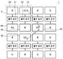
도1은 종래의 공유 구조의 CMOS 이미지 센서의 칼라필터 패턴과 출력회로간의 배치에 대하여 개괄적으로 나타낸 도면이다. 도1을 참조하면, CMOS 이미지 센서(1) 내에는 제1 그린(green)화소(10), 제1 레드(red)화소(20), 제1 블루(blue)화소(30), 제2 그린화소(40), 제 3 그린화소(50), 제4 그린화소(60)등으로 표시된 바와 같이 각 화소에서 각 수광부를 대응하여 배치되는 칼러필터의 형태로 표시하였으며, 이러한 각 화소들에 대응하는 각 수광부들은 로우(row) 방향과 칼럼(column) 방향을 따라 일정한 간격을 갖는 매트릭스 형태로 배치된다. 또한 마주보며 대응하는 2개의 화소간에는 각 화소들이 공유하는 출력회로(또는 독출회로)(21, 22)들이 존재한다.1 is a diagram schematically showing the arrangement between a color filter pattern and an output circuit of a conventional CMOS image sensor. Referring to FIG. 1, a first
CMOS 이미지 센서는 하나의 레드화소, 2개의 그린화소 및 하나의 블루화소를 하나의 색조합 단위(5)로 구성하여 칼라 색상을 구현한다. 그런데 도1에서 제1 그린화소(10)와 제2 그린화소(40) 그리고 제 2 그린화소 (40)과 제3 그린화소(50)의 위치관계를 보면, 제1 그린화소(10)와 제 2 그린화소(40)의 간격 "L1과 제2 그린화소(40)과 제3 그린화소(50)의 간격 "L2"가 동일하지 않다. 제1 그린화소(10)와 제 2 그린화소(40)의 간격(L1)이 제1 그린화소(10)와 제1 블루화소(30) 사이에 공유된 출력회로(22)에 의하여 제2 그린화소(40)와 제3 그린화소(50)의 간격(L2)보다 넓다. 따라서 전체적인 색상을 계산할 때 레드(R), 그린(G), 블루(B)의 조합에서 그린에 의하여 위치별 색상이 왜곡되어 계산될 수 있다.The CMOS image sensor implements color color by configuring one red pixel, two green pixels, and one blue pixel as one color sum unit (5). 1, the positional relationship between the first
또한 제1 그린화소(10)와 제3 그린화소(50) 또는 제1 그린화소(10)와 제4 그린화소(60)에서 발생한 전하는 제1 및 제3 그린화소(10, 50)의 제1 방향(도1에서 아랫쪽 방향)의 독출회로로 전달되고, 제2 및 제4 그린화소(40, 60)에서 발생한 전하는 제2 및 제4 그린화소(40, 80)의 제2 방향 (도1에서는 윗쪽 방향)의 독출회로로 전달된다. 따라서 반도체소자의 제조과정 중에 틸트(tilt)를 주어 수광부에 이온주입공정을 진행하는 것이 일반적이므로 각 화소의 수광부에서 발생하는 전하가 독출회로로 전달되는 양이 전하의 전달 방향에 따라 일정하지 않을 수 있다.In addition, charges generated in the first
따라서 상기와 같은 문제점들을 극복할 수 있는 CMOS 이미지 센서의 개발이 요구되어지며, 특히 고정 패턴 잡음과 앨리어싱 잡음을 감소시킨 CMOS 이미지 센서의 개발이 절실히 요구된다.Therefore, development of a CMOS image sensor capable of overcoming the above problems is required, and in particular, the development of a CMOS image sensor that reduces fixed pattern noise and aliasing noise is urgently required.
본 발명이 이루고자 하는 기술적 과제는 동일한 색상의 칼러필터가 배치되는 화소들간의 간격이 동일하도록 형성한 CMOS 이미지 센서를 제공하는데 있다.SUMMARY OF THE INVENTION The present invention has been made in an effort to provide a CMOS image sensor configured to have the same interval between pixels on which color filters of the same color are disposed.
본 발명이 이루고자 하는 다른 기술적 과제는 동일한 색상의 칼러필터가 배치되는 화소들간에 수광부에서 발생되는 전하가 동일 방향으로 전달되도록 한 CMOS 이미지 센서를 제공하는데 있다.Another object of the present invention is to provide a CMOS image sensor in which charges generated in a light receiving unit are transferred in the same direction between pixels on which color filters of the same color are disposed.
본 발명이 이루고자 하는 또다른 기술적 과제는 공유하는 출력회로를 갖는 화소들을 갖는 이미지 센서에서 같은 출력회로를 공유하는 화소와 그 화소에 인접한 화소의 사이에 다른 화소들을 공유하는 출력회로가 중간에 위치하도록 하는 CMOS 이미지 센서를 제공하는데 있다.Another technical problem to be solved by the present invention is that an image sensor having pixels having a shared output circuit is positioned so that an output circuit sharing other pixels is located between a pixel sharing the same output circuit and a pixel adjacent to the pixel. To provide a CMOS image sensor.
본 발명이 이루고자 하는 또다른 기술적 과제는 고정 패튼 잡음이 감소된 CMOS 이미지 센서를 제공하는 데 있다.Another technical object of the present invention is to provide a CMOS image sensor with reduced fixed pattern noise.
본 발명이 이루고자 하는 또다른 기술적 과제는 엘리어싱 잡음이 감소된 CMOS 이미지 센서를 제공하는 데 있다.Another technical object of the present invention is to provide a CMOS image sensor with reduced aliasing noise.
상기 목적을 달성하기 위한 본 발명의 제1 형태에 따른 CMOS 이미지 센서는, 서로 마주보는 제1 수광부 및 제2 수광부가 그들 사이에 적어도 제1 부동확산영역을 공유하면서 제1 수광부/제2 수광부 쌍을 이루며, 상기 제1 수광부/제2 수광부 쌍이 제1 방향을 따라 복수개 배열된 제1 수광부/제2 수광부 열을 이루며, 상기 제1 수광부/제2 수광부 열이 제2 방향을 따라 동일 위상에 복수개 배치되는 제1 수광부/제2 수광부 어레이 및 서로 마주보는 제3 수광부 및 제4 수광부가 그들 사이에 적어도 제2 부동확산영역을 공유하면서 제3 수광부/제4 수광부 쌍을 이루며, 상기 제3 수광부/제4 수광부 쌍이 제1 방향을 따라 복수개 배열된 제3 수광부/제4 수광부 열을 이루며, 상기 각 제3 수광부/제4 수광부 열이 제2 방향을 따라 동일 위상을 가지며 상기 제1 수광부/제2 수광부 열들 사이에 교차적으로 복수개 배치되는 제3 수광부/제4 수광부 어레이를 포함하며, 상기 제1 내지 제4 수광부는 하나의 색조합 단위를 이루도록 각 수광부 상에는 칼라필터들이 형성되며, 상기 각 수광부에서 발생되는 전하가 상기 제1 방향에서 동일한 방향으로 전달되는 한 쌍의 수광부 상에는 동일한 색상의 칼러필터가 형성된다.A CMOS image sensor according to a first aspect of the present invention for achieving the above object includes a first light receiver / second light receiver pair, with a first light receiver and a second light receiver facing each other sharing at least a first floating diffusion region therebetween. A first light receiver / second light receiver pair arranged in a plurality of first light receiver / second light receiver pairs along a first direction, and a plurality of first light receivers / second light receiver columns in a same phase along a second direction The first light receiver / second light receiver array disposed and the third light receiver and the fourth light receiver facing each other form a third light receiver / four light receiver pair while sharing at least a second floating diffusion region therebetween, and the third light receiver / A pair of fourth light receiving units forms a plurality of rows of third light receiving units / four light receiving units arranged along a first direction, and each of the third light receiving units / four light receiving units has the same phase along a second direction and the first light receiving units / second Light receiving And a plurality of third light receivers / four light receivers arranged in a plurality of rows alternately between columns, wherein the first to fourth light receivers are formed with color filters on each light receiver so as to form one color sum unit. A color filter of the same color is formed on the pair of light receiving parts in which the charges are transferred in the same direction from the first direction.
상기 각 제3 수광부/제4 수광부 열이 인접하여 배치되는 상기 제1 수광부/제2 수광부 열과는 1/2 만큼의 위상차를 가지도록 배치될 수 있으며, 상기 제1 수광부 및 상기 제4 수광부 상에 동일한 색상의 칼러필터, 예를 들어 그린필터가 형성될 수 있다.The third light receiving unit / four light receiving unit columns may be disposed to have a phase difference of 1/2 with the first light receiving unit / second light receiving unit rows disposed adjacent to each other, and on the first light receiving unit and the fourth light receiving unit. A color filter of the same color, for example, a green filter, may be formed.
또한, 상기 제1 수광부/제2 수광부 열에 배치된 하나의 제1 수광부와, 인접하여 배치된 상기 제3 수광부/제4 수광부 열에 배치되며 상기 제1 방향을 따라 상기 제1 수광부를 기준으로 전후에 배치된 두개의 상기 제4 수광부들은 등간격으로 배치되는 것이 바람직하며, 상기 각 수광부는 반도체기판내에 형성된 포토다이오드 또는 포토게이트로 구성될 수 있다.In addition, one first light receiving unit disposed in the first light receiving unit / second light receiving unit column and the third light receiving unit / four light receiving unit rows disposed adjacent to each other and in front and rear with respect to the first light receiving unit along the first direction. Preferably, the two fourth light receiving units are arranged at equal intervals, and each of the light receiving units may be formed of a photodiode or photogate formed in a semiconductor substrate.
한편, 상기 제1 수광부/제2 수광부 쌍 및 상기 제3 수광부/제4 수광부 쌍은, 이들 수광부 사이에 공유되는 출력회로의 적어도 하나의 구성요소, 예를 들어, 트랜스퍼 게이트, 리세트 게이트, 로우 선택 게이트, 증폭기 중의 적어도 하나를 더 공유할 수 있다.Meanwhile, the first light receiver / second light receiver pair and the third light receiver / four light receiver pair may include at least one component of an output circuit shared between the light receivers, for example, a transfer gate, a reset gate, and a row. At least one of the selection gate and the amplifier may be further shared.
상기 목적을 달성하기 위한 본 발명의 제2 형태에 따른 CMOS 이미지 센서는, 서로 마주보는 제1 수광부 및 제2 수광부가 그들 사이에 출력회로의 적어도 하나의 구성요소를 공유하면서 제1 수광부/제2 수광부 쌍을 이루며, 상기 제1 수광부/제2 수광부 쌍이 제1 방향을 따라 복수개 배열된 제1 수광부/제2 수광부 열을 이루며, 상기 제1 수광부/제2 수광부 열이 제2 방향을 따라 동일 위상에 복수개 배치되는 제1 수광부/제2 수광부 어레이 및 서로 마주보는 제3 수광부 및 제4 수광부가 그들 사이에 출력회로의 적어도 하나의 구성요소를 공유하면서 제3 수광부/제4 수광부 쌍을 이루며, 상기 제3 수광부/제4 수광부 쌍이 제1 방향을 따라 복수개 배열된 제3 수광부/제4 수광부 열을 이루며, 상기 각 제3 수광부/제4 수광부 열이 제2 방향을 따라 동일 위상을 가지며 상기 제1 수광부/제2 수광부 열들 사이에서 교차적으로 복수개 배치되는 제3 수광부/제4 수광부 어레이를 포함하며, 상기 각 제3 수광부/제4 수광부 열이 인접하여 배치되는 상기 제1 수광부/제2 수광부 열과는 1/2 만큼의 위상차를 가지도록 배치된다.A CMOS image sensor according to a second aspect of the present invention for achieving the above object includes a first light receiver / second light receiver while a first light receiver and a second light receiver facing each other share at least one component of an output circuit therebetween. Forming a pair of light receiving units, wherein the first light receiving unit / second light receiving unit pair is arranged in a plurality of first light receiving unit / second light receiving unit rows arranged in a first direction, and the first light receiving unit / second light receiving unit columns are in phase with the second direction; A plurality of first light receiving units / second light receiving arrays disposed in the plurality of light receiving units and a third light receiving unit facing each other and a fourth light receiving unit share at least one component of an output circuit therebetween, forming a third light receiving unit / four light receiving unit pairs; The third light receiver / four light receiver pairs form a plurality of third light receivers / four light receivers arranged along a first direction, and each of the third light receivers / four light receivers has the same phase along the second direction. And a third light receiver / four light receiver array arranged in a plurality of rows alternately between the first light receiver / second light receiver columns, wherein each of the third light receiver / four light receiver columns is adjacent to each other. The light receiving unit is arranged to have a phase difference by 1/2.
상기 제1 내지 제4 수광부는 하나의 색조합 단위를 이루도록 각 수광부 상에는 칼라필터들이 형성되며, 상기 각 수광부에서 발생되는 전하가 상기 제1 방향에서 동일한 방향으로 전달되는 한 쌍의 수광부 상에는 동일한 색상의 칼러필터, 예 를 들어 상기 제1 수광부 및 제4 수광부 상에는 그린필터가 형성될 수 있다.Color filters are formed on each light receiving unit so that the first to fourth light receiving units form one color sum unit, and the same color is applied to a pair of light receiving units in which charges generated from the light receiving units are transmitted in the same direction in the first direction. A green filter may be formed on the color filter, for example, the first light receiving part and the fourth light receiving part.
또한, 상기 제1 수광부/제2 수광부 열에 배치된 하나의 제1 수광부와, 인접하여 배치된 상기 제3 수광부/제4 수광부 열에 배치되며 상기 제1 방향을 따라 상기 제1 수광부를 기준으로 전후에 배치된 두개의 상기 제4 수광부들은 등간격으로 배치되는 것이 바람직하며, 상기 각 수광부는 반도체기판내에 형성된 포토다이오드 또는 포토게이트로 구성될 수 있다.In addition, one first light receiving unit disposed in the first light receiving unit / second light receiving unit column and the third light receiving unit / four light receiving unit rows disposed adjacent to each other and in front and rear with respect to the first light receiving unit along the first direction. Preferably, the two fourth light receiving units are arranged at equal intervals, and each of the light receiving units may be formed of a photodiode or photogate formed in a semiconductor substrate.
한편, 상기 제1 수광부/제2 수광부 쌍 및 상기 제3 수광부/제4 수광부 쌍은, 이들 수광부 사이에 공유되는 출력회로의 적어도 하나의 구성요소, 예를 들어, 부동확산영역, 트랜스퍼 게이트, 리세트 게이트, 로우 선택 게이트, 증폭기 중의 적어도 하나를 더 공유할 수 있다.Meanwhile, the first light receiver / second light receiver pair and the third light receiver / four light receiver pair may include at least one component of an output circuit shared between the light receivers, for example, a floating diffusion region, a transfer gate, and a receiver. At least one of the set gate, the row select gate, and the amplifier may be further shared.
본 발명에 따르면, 하나의 색조합 단위에서 동일한 색상의 칼러필터가 배치되는 수광부들에서 발생되는 전하가 동일한 방향으로 전달되도록 하기 때문에 CMOS 이미지 센서의 전기적, 광학적 특성이 균일하게 유지되어 모자이크 형태의 고정 잡음 패턴이 매우 감소될 수 있다.According to the present invention, since the electric charges generated in the light receiving parts in which the color filters of the same color are disposed in one color sum unit are transferred in the same direction, the electrical and optical characteristics of the CMOS image sensor are uniformly maintained to fix the mosaic shape. The noise pattern can be greatly reduced.
또한 본 발명에 따르면, 하나의 색조합 단위에서 동일한 색상의 칼러필터가 배치되는 수광부들간의 간격이 등간격으로 되어 공간 샘플링이 균일하게 이루어질 수 있기 때문에 엘리어싱 잡음을 최소화할 수 있다.In addition, according to the present invention, since the intervals between the light receiving units in which the color filters of the same color are arranged in one tonal sum unit are equally spaced, the spatial sampling can be made uniform, thereby eliminating the aliasing noise.
이하, 첨부한 도면을 참조하여 본 발명의 바람직한 실시예들을 상세하게 설명한다. 그러나, 본 발명은 많은 상이한 형태로 구현될 수 있으며, 여기서 설명되는 실시예들에 한정되는 것으로 해석되서는 아니되며, 차라리 이러한 실시예들은 그 개시내용을 완벽히 하며 발명의 사상을 당업자에게 충분히 전달하기 위해 제공되는 것이다. 도면들에서, 층들 및 영역들의 두께는 명료성을 위해 과장되어 있다. 동일한 참조번호는 전체적으로 동일한 요소를 지칭한다.Hereinafter, exemplary embodiments of the present invention will be described in detail with reference to the accompanying drawings. However, the present invention may be embodied in many different forms and should not be construed as limited to the embodiments set forth herein, rather these embodiments are intended to complete the disclosure and to fully convey the spirit of the invention to those skilled in the art. It is provided for. In the drawings, the thicknesses of layers and regions are exaggerated for clarity. Like numbers refer to like elements throughout.
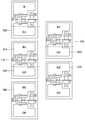
도2는 본 발명의 하나의 실시예에 따른 CMOS 이미지 센서(100)에서 칼러필터가 배치되는 각 화소의 수광부와 이들 사이에서 공유되는 출력회로들간의 배치관계를 개략적으로 나타내는 도면이다. 도2의 이미지 센서(100)는 레드 칼러필터가 배치되는 1개의 레드(red) 화소영역, 그린 칼러필터가 배치되는 2개의 그린(green) 화소영역 및 블루 칼러필터가 배치되는 1개의 블루(blue) 화소영역을 가지고 이들 색상을 조합하여 영상신호를 검출하는 베이어 칼라 필터 어레이 (Bayer color filter array)를 나타낸다.FIG. 2 is a diagram schematically illustrating an arrangement relationship between a light receiving unit of each pixel in which a color filter is disposed in a
도2를 참조하면, 1개의 레드 화소영역(380), 2개의 그린 화소영역(340, 350)와 1개의 블루 화소영역(310)이 색상을 계산하는 하나의 색조합 세트로 작용한다. 특히, 제1 방향(도면의 수직방향)으로 레드 화소영역(380) 및 제4 그린 화소영역(350)은 그 사이에 하나의 출력회로(130)를 공유하면서 대칭적인 구조를 갖는 레드 화소영역(380)/제4 그린 화소영역(350) 쌍(200)을 이루며, 제1 방향을 따라 레드 화소영역(380)/제4 그린 화소영역(350) 쌍(200)이 복수개 형성되어 레드 화소영역(380)/제4 그린 화소영역(350) 열을 형성하며, 이러한 레드 화소영역(380)/제4 그린 화소영역(350) 열이 제1 방향에 직교하는 제2 방향(도면의 수평방향)을 따라 일정한 간격을 가지며 매트릭스 형태로 동일 위상에 복수개 형성되어 레드 화소영역(380)/제4 그린 화소영역(350) 어레이를 형성한다.Referring to FIG. 2, one
또한, 하나의 레드 화소영역(380)/제4 그린 화소영역(350) 열에 인접하여 제1 방향(도면의 수직방향)으로 블루 화소영역(310) 및 제3 그린 화소영역(350)은 그 사이에 하나의 출력회로(110)를 공유하면서 대칭적인 구조를 갖는 블루 화소영역(310)/제3 그린 화소영역(340) 쌍(400)을 이루며, 제1 방향을 따라 레드 화소영역(310)/제3 그린 화소영역(340) 쌍(400)이 복수개 형성되어 레드 화소영역(310)/제3 그린 화소영역(340) 열을 형성하며, 이러한 레드 화소영역(310)/제3 그린 화소영역(340) 열이 제1 방향에 직교하는 제2 방향(도면의 수평방향)을 따라 일정한 간격을 가지며 매트릭스 형태로 동일 위상에 복수개 형성되고, 각 레드 화소영역(380)/제4 그린 화소영역(350) 열과는 교차적으로 배치되는 블루 화소영역(310)/제3 그린 화소영역(340) 어레이를 형성한다. 이러한 레드 화소영역(380)/제4 그린 화소영역(350) 어레이와 블루 화소영역(310)/제3 그린 화소영역(340) 어레이에 의해 전체 CMOS 이미지 센서가 구성된다.In addition, the
본 발명의 하나의 실시예에서는, 전술한 종래의 CMOS 이미지 센서의 배치와 달리 레드 화소영역(380)/제4 그린 화소영역(350) 어레이와 블루 화소영역(310)/제3 그린 화소영역(340) 어레이가 서로 1/2 위상차가 발생되도록 서로 엇갈리는 형태로 배치된다. 본 실시예에서는 레드 화소영역(380)/제4 그린 화소영역(350) 쌍(200)과 블루 화소영역(310)/제3 그린 화소영역(340) 쌍(400)이 하나의 색조합 단위를 구성한다.According to one embodiment of the present invention, unlike the arrangement of the conventional CMOS image sensor described above, the
본 실시예에서는 레드 화소영역(380)/제4 그린 화소영역(350) 어레이와 블루 화소영역(310)/제3 그린 화소영역(340) 어레이가 서로 1/2 위상차가 발생하도록 배 치함으로써, 인접하는 레드 화소영역(380)/제4 그린 화소영역(350) 열과 블루 화소영역(310)/제3 그린 화소영역(340) 열의 관계에서 그린 화소영역들간의 간격 "L3"이 동일하게 된다. 즉 제1 그린 화소영역(300)과 제2 그린 화소영역(320) 간의 간격과, 제2 그린 화소영역(320)과 제3 그린 화소영역(340) 간의 간격이 등간격으로 배치된다.In the present exemplary embodiment, the
또한, 본 실시예에서는 각 색조합 단위에서 동일한 색상의 칼러필터가 배치되는 화소들에서 발생된 전하들이 이들 화소들로부터 출력회로들로 전달되는 전하의 이동방향이 동일하도록 배치된다. 보다 구체적으로는, 레드 화소영역(380)/제4 그린 화소영역(350) 쌍(200)과 블루 화소영역(310)/제3 그린 화소영역(340) 쌍(400)이 하나의 색조합 단위를 이루며, 이 색조합 단위내에서 동일한 색상의 그린 칼러필터가 배치되는 제4 그린 화소영역(350)과 제3 그린 화소영역(340)내에서 빛의 입사에 의해 발생되는 전하가 각기 동일한 방향(도면에서 상측 방향)으로 이동한다. 즉 레드 화소영역(380)/제4 그린 화소영역(350) 쌍(200)에서는 제4 그린 화소영역(350)내의 수광부에서 발생된 전하가 이들 사이에 배치된 출력회로(130)를 향하여 상측방향으로 전달되며, 블루 화소영역(310)/제3 그린 화소영역(340) 쌍(400)에서는 제3 그린 화소영역(340)내의 수광부에서 발생된 전하가 이들 사이에 배치된 출력회로(110)를 향하여 상측방향으로 전달된다. 따라서 레드 화소영역(380)/제4 그린 화소영역(350) 쌍(200)과 블루 화소영역(310)/제3 그린 화소영역(340) 쌍(400)으로 구성되는 하나의 색조합 단위 내 및 전체 이미지 센서에서 각 그린 화소영역에서 비록 빛이 경사져 입사되어도 각 그린 화소영역의 전기적, 광학 적 특성이 균일하게 유지될 수 있다.Further, in the present embodiment, the charges generated in the pixels in which the color filters of the same color are arranged in each color sum unit are arranged so that the direction of movement of the charges transferred from these pixels to the output circuits is the same. More specifically, the
따라서, 각 화소가 편중되어 왜곡된 화상을 나타내는 것을 막을 수 있다. 또한 그린 화소영역과 출력회로의 위치가 그린 화소영역 내에서 발생한 전하가 출력회로로 이동하는 방향이 동일한 형태를 갖기 때문에, 반도체소자의 제조공정에서 틸트(tilt)를 주어 이온주입하는 공정, 미스얼라인 시 한쪽 방향으로 패턴이 치우치는 현상, 특히 카메라폰 등에서 렌즈와 이미지 센서간의 거리가 짧기 때문에 사광 입사 시 그림자가 지는 현상 등으로 더욱 심각하게 발생하는 동일한 그린 화소영역간의 전기적, 광학적 특성적 차이를 줄일 수 있다. 좀 더 자세히 보면 동일한 색상의 칼러필터가 배치되는 화소영역 사이에 전하를 이송시키는 트랜스퍼 게이트의 아래에서 전하의 이동 방향이 달라짐에 따라 발생되는 각 화소영역간의 특성 차이를 현저히 줄일 수 있다. 도2에서는 예를 들어 2개의 화소영역을 대칭적으로 공유하는 출력회로를 제시하고 있지만, 4개의 화소 영역을 공유하는 출력회로 및 6개의 화소영역을 공유하는 출력회로에도 동일한 원리가 적용될 수 있다.Therefore, it is possible to prevent each pixel from displaying a distorted and distorted image. In addition, since the positions of the green pixel region and the output circuit have the same direction in which charges generated in the green pixel region move to the output circuit, the process of implanting ions by giving a tilt in the manufacturing process of the semiconductor device is misaligned. Reduces the electrical and optical characteristic differences between the same green pixel areas caused by the pattern bias in one direction, especially the camera lens, etc., because the distance between the lens and the image sensor is short, which causes the shadow to be blurred when incident light is incident. Can be. In more detail, the difference in characteristics between the pixel areas generated as the direction of charge movement is changed under the transfer gate for transferring charges between the pixel areas in which the color filters of the same color are disposed may be significantly reduced. In Fig. 2, for example, an output circuit that shares two pixel regions symmetrically is shown. However, the same principle may be applied to an output circuit that shares four pixel regions and an output circuit that shares six pixel regions.
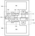
도3은 도2의 각 칼라필터 하부에 존재하는 수광부와 인접한 수광부 사이에 배치되는 출력회로의 하나의 예를 표시한 도면이며, 도4는 도3에서 인접하여 배치된 2개의 수광부와 그들 사이에 배치되는 출력회로를 보다 구체적으로 표시한 도면이다.FIG. 3 is a view showing an example of an output circuit disposed between the light receiving portions existing below each color filter of FIG. 2 and the adjacent light receiving portions, and FIG. 4 shows two light receiving portions disposed adjacent to each other in FIG. More specifically, the output circuit is arranged.
도3 및 도4를 참조하면, 각 화소영역 쌍에서 대칭되는 두개의 화소영역들이 부동확산(floating diffusion)영역을 공유하는 레이아웃의 구조을 제시하고 있다. 각 화소영역의 수광부들은 반도체기판내에서 소정의 불순물이온이 주입된 액티브 영역이고, 출력회로를 공유하는 이들 화소영역들 사이는 아이솔레이션(isolation)영역이 된다. 각 화소영역들은 반도체 기판에 형성되는데 각 화소영역에는 외부에서의 빛을 전하, 예를 들어 전자로 변화하는 포토다이오드 (photodiode) 또는 포토게이트(photo gate) 형태의 수광부(310, 340)가 형성되어 있다.3 and 4, a layout structure in which two symmetrical pixel regions in each pixel region pair share a floating diffusion region is shown. The light-receiving portions of each pixel region are active regions in which predetermined impurity ions are implanted in the semiconductor substrate, and an isolation region is formed between these pixel regions sharing the output circuit. Each pixel region is formed on a semiconductor substrate. In each pixel region, light receiving
도4에서 블루 칼러필터가 그 상측에 배치되는 제1 수광부(310)와 그린 칼러필터가 그 상측에 배치되는 제2 수광부(340)는 그 사이에 출력회로(110)를 공유하면서 대칭적으로 배치된다. 제1 수광부(310)내에서 발생된 전자는 제1 트랜스퍼 게이트(112)에 의해 출력회로(110)내의 구성요소의 하나인 부동확산영역(118)로 이송되며, 제2 수광부(340)내에서 발생된 전자는 제2 트랜스퍼 게이트(113)에 의해 부동확산영역(118)으로 이송된다.In FIG. 4, the first
제1 수광부(310)과 제2 수광부(340) 사이에서 공유되는 출력회로(110)는 CMOS 이미지 센서의 종류에 따라 다양하게 설계될 수 있으며, 도4에서는 대표적으로 트랜스퍼 게이트(112, 113), 하나의 공유된 부동확산영역(118), 리셋 게이트 (reset gate,114), 전원전압(115), 소오스 팔로우 게이트(source follow gate, 116) 및 로우 선택 게이트(row select gate,117)을 나타내고 있다. 제1 수광부(310)와 제2 수광부(340)는 빛을 받아서 전자를 발생시키는 광집적기 예를 들면, 포토다이오드 또는 포오토 게이트가 위치하고 있다. 발생된 전자는 예를 들어, 각각 폴리실리콘으로 형성된 트랜스퍼 게이트(112, 113)의 동작에 의하여 부동확산영역(118)으로 이송된다.The
한편, 출력회로(110)는 부동확산영역(118)을 공유할 수도 있고, 소오스 팔로 우 소자(source follow), 리셋 게이트를 선택적으로 공유할 수도 있다. 바람직하게는 반도체 칩의 면적을 줄이기 위해 부동확산영역, 소우스 팔로우 게이트, 리셋 게이트를 공유시키는 것이 바람직하다.Meanwhile, the
동작 측면에서 보면, 일반적인 CMOS 이미지 센서의 출력회로에 기초한다. 부동확산영역으로 이송된 전하는 리세트 게이트를 온(on)시켜서 전원전압과 연결시켜 전하를 빼고, 리세트 게이트를 끊고 트랜스퍼 게이트를 온시켜 포오토 다이오드와 같은 소자가 있는 수광부에서 발생한 전자를 부동확산영역으로 이송시켜서 리세트 게이트가 온된 상태의 전압에서 트랜스퍼 게이트를 온시켜 부동확산영역에 전하를 축적한 후의 전압과의 차이를 가지고 이것을 에이디컨버터(ADC)를 통해 신호를 보낸다. 본 발명에 제시하는 이미지 센서는 블루, 그린, 레드를 하나의 색조합 단위를 구성하는 칼라필터 패턴으로 제시하고 있지만, 마젠타 (magenta), 사이엔 (cyan), 옐로우 (yellow)를 하나의 색조합 단위로 할 수 있다. 상기의 트랜스퍼 게이트, 리세트 게이트 및 소오스 팔로우 게이트는 폴리실리콘으로 형성되어 있으며, 각 화소영역내의 포토 다이오드는 핀드 포오토 다이오드 (pinned photo diode)로 구성되어 있어 n형의 영역에서 전자가 축적될 수 있다. 부동확산영역 n형 도펀트(dopant)가 이온 주입된 영역일 수 있다. 각 화소의 영역 위쪽에는 수지(resin)성분으로된 칼라 필터가 형성되어 있으며, 칼라 필터의 상부에는 마이크로 렌즈(microlens)가 형성되어 있어 외부에서 들어 오는 빛을 포오토다이오드와 같은 광집기 방향으로 집광하게 해준다.In terms of operation, it is based on the output circuit of a typical CMOS image sensor. The charge transferred to the floating diffusion region turns on the reset gate to connect with the power supply voltage to remove the charge, disconnects the reset gate, turns on the transfer gate, and floats the electrons generated in the light receiving part having a device such as a photodiode. The transfer gate is turned on at the voltage at which the reset gate is turned on, and the signal is transmitted through the AD converter ADC with a difference from the voltage after accumulating charge in the floating diffusion region. The image sensor proposed in the present invention presents blue, green, and red as color filter patterns constituting a single color sum unit, but magenta, cyan, and yellow are one color sum. Can be in units. The transfer gate, the reset gate, and the source follow gate are formed of polysilicon, and the photodiodes in each pixel region are composed of pinned photo diodes so that electrons can accumulate in the n-type region. have. The floating diffusion region n-type dopant may be an ion implanted region. A color filter made of a resin component is formed above each pixel area, and microlens is formed on the upper part of the color filter to collect light from the outside in a light-collecting direction such as a photodiode. Let's do it.
이상은 본 발명의 바람직한 실시예에 대한 구체적인 설명이지만, 본 발명은 상기 실시예들의 형태에 한정되는 것이 아니라 본 발명의 기술적 사상을 벗어나지 않는 범위내에서 당업자의 기술수준에 따라 여러 가지로 변경을 가하는 것이 가능하다. 즉, 본 발명의 실시예는 R, G, B가 베이어 패턴으로 배치되는 경우에 대하여 설명하였지만, 베이어 패턴과 비슷한 유형으로 배치되는 다이아고날 스트라이프 패턴(diagonal stripe pattern)에도 적용될 수 있음은 물론이며, 본 실시예에서는 보다 자연스러운 색상의 구현에 유리한 그린 칼러필터를 색조합 단위에 2개 포함된 구조에 대하여 설명하였지만, 그린 색상 이외의 색상이 하나의 색조합 단위에서 2개 포함되는 것을 배제하는 것은 아니다. 또한, 본 발명에서 출력회로로 표시되는 것은 본 실시예의 구성요소에 한정되지 않고, 각종 CMOS 이미지 센서의 종류에 따라 구비되는 출력회로의 구성요소들을 모두 포함하는 개념이다.Although the above is a detailed description of a preferred embodiment of the present invention, the present invention is not limited to the form of the embodiments, but various changes depending on the skill level of those skilled in the art without departing from the technical spirit of the present invention It is possible. That is, although the embodiment of the present invention has been described with respect to the case in which the R, G, and B are arranged in the Bayer pattern, the embodiment may be applied to a diagonal stripe pattern arranged in a similar type to the Bayer pattern. In the present exemplary embodiment, the structure in which two green color filters are included in the tonal sum unit, which is advantageous for realizing more natural colors, has been described. However, it is not excluded that two colors other than the green color are included in one tonal sum unit. . In addition, in the present invention, the output circuit is not limited to the components of the exemplary embodiment, and is a concept including all the components of the output circuit provided according to various types of CMOS image sensors.
본 발명에 의하면, 하나의 색조합 단위에서 동일한 색상의 칼러필터가 배치되는 수광부들에서 발생되는 전하가 동일한 방향으로 전달되기 때문에 CMOS 이미지 센서의 각 화소에서 전기적, 광학적 특성이 균일하게 유지되어 모자이크 형태의 고정 잡음 패턴이 감소된다.According to the present invention, since electric charges generated in the light receiving parts in which the color filters of the same color are arranged in one color sum unit are transferred in the same direction, the electrical and optical characteristics are uniformly maintained in each pixel of the CMOS image sensor to form a mosaic. The fixed noise pattern of is reduced.
또한 본 발명에 의하면, 하나의 색조합 단위에서 동일한 색상의 칼러필터가 배치되는 수광부들간의 간격이 등간격으로 되어 공간 샘플링이 균일하게 이루어질 수 있기 때문에 엘리어싱 잡음을 최소화할 수 있다.In addition, according to the present invention, since the intervals between the light receiving units where the color filters of the same color are arranged in one tonal sum unit are equally spaced, spatial sampling can be made uniform, thereby eliminating aliasing noise.
Claims (19)
Translated fromKoreanPriority Applications (2)
| Application Number | Priority Date | Filing Date | Title |
|---|---|---|---|
| KR1020040101140AKR100674923B1 (en) | 2004-12-03 | 2004-12-03 | CMOS image sensor shares output circuits between adjacent pixels |
| US11/291,218US20060119715A1 (en) | 2004-12-03 | 2005-12-01 | CMOS image sensor sharing readout circuits between adjacent pixels |
Applications Claiming Priority (1)
| Application Number | Priority Date | Filing Date | Title |
|---|---|---|---|
| KR1020040101140AKR100674923B1 (en) | 2004-12-03 | 2004-12-03 | CMOS image sensor shares output circuits between adjacent pixels |
Publications (2)
| Publication Number | Publication Date |
|---|---|
| KR20060062334A KR20060062334A (en) | 2006-06-12 |
| KR100674923B1true KR100674923B1 (en) | 2007-01-26 |
Family
ID=36573718
Family Applications (1)
| Application Number | Title | Priority Date | Filing Date |
|---|---|---|---|
| KR1020040101140AExpired - Fee RelatedKR100674923B1 (en) | 2004-12-03 | 2004-12-03 | CMOS image sensor shares output circuits between adjacent pixels |
Country Status (2)
| Country | Link |
|---|---|
| US (1) | US20060119715A1 (en) |
| KR (1) | KR100674923B1 (en) |
Cited By (1)
| Publication number | Priority date | Publication date | Assignee | Title |
|---|---|---|---|---|
| KR101313689B1 (en)* | 2011-12-19 | 2013-10-02 | 주식회사 동부하이텍 | Image sensor |
Families Citing this family (10)
| Publication number | Priority date | Publication date | Assignee | Title |
|---|---|---|---|---|
| JP4695979B2 (en)* | 2005-12-26 | 2011-06-08 | パナソニック株式会社 | Solid-state imaging device |
| KR100858033B1 (en) | 2007-10-15 | 2008-09-10 | (주)실리콘화일 | 4T-4S step & repeat unit pixel and image sensor having the unit pixel |
| JP5026951B2 (en)* | 2007-12-26 | 2012-09-19 | オリンパスイメージング株式会社 | Imaging device driving device, imaging device driving method, imaging device, and imaging device |
| GB2466213B (en)* | 2008-12-12 | 2013-03-06 | Cmosis Nv | Pixel array with shared readout circuitry |
| US8547458B2 (en) | 2009-02-04 | 2013-10-01 | Rosnes Corporation | Solid-state image pickup device |
| US8576312B2 (en)* | 2009-02-04 | 2013-11-05 | Rosnes Corporation | Solid-state image pickup device with particular pixel arrangement |
| KR102541701B1 (en)* | 2016-01-15 | 2023-06-13 | 삼성전자주식회사 | CMOS Image Sensor |
| CN109659329A (en)* | 2019-01-25 | 2019-04-19 | 上海晔芯电子科技有限公司 | Imaging sensor with shared structure pixel layout |
| CN110709992A (en)* | 2019-08-27 | 2020-01-17 | 深圳市汇顶科技股份有限公司 | Semiconductor structure, chip and electronic device of image sensor |
| KR102820466B1 (en) | 2019-12-13 | 2025-06-17 | 삼성전자주식회사 | Image senosor, image device having the same, and operating method therof |
Family Cites Families (25)
| Publication number | Priority date | Publication date | Assignee | Title |
|---|---|---|---|---|
| US4918869A (en)* | 1987-10-28 | 1990-04-24 | Fujikoshi Machinery Corporation | Method for lapping a wafer material and an apparatus therefor |
| JP2993144B2 (en)* | 1991-02-22 | 1999-12-20 | 株式会社デンソー | Image sensor |
| US5624299A (en)* | 1993-12-27 | 1997-04-29 | Applied Materials, Inc. | Chemical mechanical polishing apparatus with improved carrier and method of use |
| US5643053A (en)* | 1993-12-27 | 1997-07-01 | Applied Materials, Inc. | Chemical mechanical polishing apparatus with improved polishing control |
| US5908530A (en)* | 1995-05-18 | 1999-06-01 | Obsidian, Inc. | Apparatus for chemical mechanical polishing |
| US6036587A (en)* | 1996-10-10 | 2000-03-14 | Applied Materials, Inc. | Carrier head with layer of conformable material for a chemical mechanical polishing system |
| US6056632A (en)* | 1997-02-13 | 2000-05-02 | Speedfam-Ipec Corp. | Semiconductor wafer polishing apparatus with a variable polishing force wafer carrier head |
| US6080050A (en)* | 1997-12-31 | 2000-06-27 | Applied Materials, Inc. | Carrier head including a flexible membrane and a compliant backing member for a chemical mechanical polishing apparatus |
| US6977684B1 (en)* | 1998-04-30 | 2005-12-20 | Canon Kabushiki Kaisha | Arrangement of circuits in pixels, each circuit shared by a plurality of pixels, in image sensing apparatus |
| US5985094A (en)* | 1998-05-12 | 1999-11-16 | Speedfam-Ipec Corporation | Semiconductor wafer carrier |
| US6106379A (en)* | 1998-05-12 | 2000-08-22 | Speedfam-Ipec Corporation | Semiconductor wafer carrier with automatic ring extension |
| US6159079A (en)* | 1998-09-08 | 2000-12-12 | Applied Materials, Inc. | Carrier head for chemical mechanical polishing a substrate |
| US6210255B1 (en)* | 1998-09-08 | 2001-04-03 | Applied Materials, Inc. | Carrier head for chemical mechanical polishing a substrate |
| US6132298A (en)* | 1998-11-25 | 2000-10-17 | Applied Materials, Inc. | Carrier head with edge control for chemical mechanical polishing |
| US6277014B1 (en)* | 1998-10-09 | 2001-08-21 | Applied Materials, Inc. | Carrier head with a flexible membrane for chemical mechanical polishing |
| US6244942B1 (en)* | 1998-10-09 | 2001-06-12 | Applied Materials, Inc. | Carrier head with a flexible membrane and adjustable edge pressure |
| US6165058A (en)* | 1998-12-09 | 2000-12-26 | Applied Materials, Inc. | Carrier head for chemical mechanical polishing |
| US6422927B1 (en)* | 1998-12-30 | 2002-07-23 | Applied Materials, Inc. | Carrier head with controllable pressure and loading area for chemical mechanical polishing |
| US6162116A (en)* | 1999-01-23 | 2000-12-19 | Applied Materials, Inc. | Carrier head for chemical mechanical polishing |
| US6358121B1 (en)* | 1999-07-09 | 2002-03-19 | Applied Materials, Inc. | Carrier head with a flexible membrane and an edge load ring |
| US20040005842A1 (en)* | 2000-07-25 | 2004-01-08 | Chen Hung Chih | Carrier head with flexible membrane |
| US6676497B1 (en)* | 2000-09-08 | 2004-01-13 | Applied Materials Inc. | Vibration damping in a chemical mechanical polishing system |
| JP3520916B2 (en)* | 2000-12-25 | 2004-04-19 | 株式会社東京精密 | Wafer polishing equipment |
| JP2005005573A (en)* | 2003-06-13 | 2005-01-06 | Fujitsu Ltd | Imaging device |
| JP2006005711A (en)* | 2004-06-18 | 2006-01-05 | Iwate Toshiba Electronics Co Ltd | CMOS image sensor |
- 2004
- 2004-12-03KRKR1020040101140Apatent/KR100674923B1/ennot_activeExpired - Fee Related
- 2005
- 2005-12-01USUS11/291,218patent/US20060119715A1/ennot_activeAbandoned
Cited By (1)
| Publication number | Priority date | Publication date | Assignee | Title |
|---|---|---|---|---|
| KR101313689B1 (en)* | 2011-12-19 | 2013-10-02 | 주식회사 동부하이텍 | Image sensor |
Also Published As
| Publication number | Publication date |
|---|---|
| US20060119715A1 (en) | 2006-06-08 |
| KR20060062334A (en) | 2006-06-12 |
Similar Documents
| Publication | Publication Date | Title |
|---|---|---|
| US11348953B2 (en) | Solid-state image sensor and camera | |
| US11223788B2 (en) | Image sensor including at least one autofocusing pixel and at least one normal pixel and driving method thereof | |
| US11114492B2 (en) | Image sensor | |
| KR102437162B1 (en) | Image sensor | |
| KR101863505B1 (en) | Solid-state imaging device and electronic apparatus | |
| US20200020730A1 (en) | High dynamic range pixel using light separation | |
| KR101683296B1 (en) | Solid-state imaging device, manufacturing method thereof, and electronic apparatus | |
| EP1026747B1 (en) | Image sensor | |
| KR101068698B1 (en) | Solid-state imaging device | |
| US20090021629A1 (en) | Solid state imaging device | |
| US6359323B1 (en) | Color image sensor and method for fabricating the same | |
| EP2255389B1 (en) | Stacked image sensor with shared diffusion regions | |
| CN107706200A (en) | Imaging sensor | |
| KR20200119672A (en) | Image sensors including shared pixels | |
| KR100674923B1 (en) | CMOS image sensor shares output circuits between adjacent pixels | |
| KR20230050330A (en) | Solid-state imaging devices and electronic devices | |
| KR100837454B1 (en) | Solid-state image sensing device | |
| US20060125947A1 (en) | Imaging with clustered photosite arrays | |
| US11626387B2 (en) | Image sensing device | |
| US20230299096A1 (en) | Image sensor and manufacturing method of the same | |
| TW202516941A (en) | Image sensing device | |
| KR19990018939A (en) | Charge Coupled Image Sensor |
Legal Events
| Date | Code | Title | Description |
|---|---|---|---|
| A201 | Request for examination | ||
| PA0109 | Patent application | St.27 status event code:A-0-1-A10-A12-nap-PA0109 | |
| PA0201 | Request for examination | St.27 status event code:A-1-2-D10-D11-exm-PA0201 | |
| R17-X000 | Change to representative recorded | St.27 status event code:A-3-3-R10-R17-oth-X000 | |
| PN2301 | Change of applicant | St.27 status event code:A-3-3-R10-R13-asn-PN2301 St.27 status event code:A-3-3-R10-R11-asn-PN2301 | |
| PN2301 | Change of applicant | St.27 status event code:A-3-3-R10-R13-asn-PN2301 St.27 status event code:A-3-3-R10-R11-asn-PN2301 | |
| D13-X000 | Search requested | St.27 status event code:A-1-2-D10-D13-srh-X000 | |
| D14-X000 | Search report completed | St.27 status event code:A-1-2-D10-D14-srh-X000 | |
| PG1501 | Laying open of application | St.27 status event code:A-1-1-Q10-Q12-nap-PG1501 | |
| E902 | Notification of reason for refusal | ||
| PE0902 | Notice of grounds for rejection | St.27 status event code:A-1-2-D10-D21-exm-PE0902 | |
| E13-X000 | Pre-grant limitation requested | St.27 status event code:A-2-3-E10-E13-lim-X000 | |
| P11-X000 | Amendment of application requested | St.27 status event code:A-2-2-P10-P11-nap-X000 | |
| P13-X000 | Application amended | St.27 status event code:A-2-2-P10-P13-nap-X000 | |
| E701 | Decision to grant or registration of patent right | ||
| PE0701 | Decision of registration | St.27 status event code:A-1-2-D10-D22-exm-PE0701 | |
| GRNT | Written decision to grant | ||
| PR0701 | Registration of establishment | St.27 status event code:A-2-4-F10-F11-exm-PR0701 | |
| PR1002 | Payment of registration fee | St.27 status event code:A-2-2-U10-U11-oth-PR1002 Fee payment year number:1 | |
| PG1601 | Publication of registration | St.27 status event code:A-4-4-Q10-Q13-nap-PG1601 | |
| PR1001 | Payment of annual fee | St.27 status event code:A-4-4-U10-U11-oth-PR1001 Fee payment year number:4 | |
| PR1001 | Payment of annual fee | St.27 status event code:A-4-4-U10-U11-oth-PR1001 Fee payment year number:5 | |
| PR1001 | Payment of annual fee | St.27 status event code:A-4-4-U10-U11-oth-PR1001 Fee payment year number:6 | |
| R18-X000 | Changes to party contact information recorded | St.27 status event code:A-5-5-R10-R18-oth-X000 | |
| FPAY | Annual fee payment | Payment date:20130102 Year of fee payment:7 | |
| PR1001 | Payment of annual fee | St.27 status event code:A-4-4-U10-U11-oth-PR1001 Fee payment year number:7 | |
| FPAY | Annual fee payment | Payment date:20140103 Year of fee payment:8 | |
| PR1001 | Payment of annual fee | St.27 status event code:A-4-4-U10-U11-oth-PR1001 Fee payment year number:8 | |
| LAPS | Lapse due to unpaid annual fee | ||
| PC1903 | Unpaid annual fee | St.27 status event code:A-4-4-U10-U13-oth-PC1903 Not in force date:20150123 Payment event data comment text:Termination Category : DEFAULT_OF_REGISTRATION_FEE | |
| PC1903 | Unpaid annual fee | St.27 status event code:N-4-6-H10-H13-oth-PC1903 Ip right cessation event data comment text:Termination Category : DEFAULT_OF_REGISTRATION_FEE Not in force date:20150123 | |
| P22-X000 | Classification modified | St.27 status event code:A-4-4-P10-P22-nap-X000 | |
| P22-X000 | Classification modified | St.27 status event code:A-4-4-P10-P22-nap-X000 |