KR100672909B1 - Sls 방법에 의한 처리중 및 처리후의 실리콘 박막의표면 평탄화 - Google Patents
Sls 방법에 의한 처리중 및 처리후의 실리콘 박막의표면 평탄화Download PDFInfo
- Publication number
- KR100672909B1 KR100672909B1KR1020017014881AKR20017014881AKR100672909B1KR 100672909 B1KR100672909 B1KR 100672909B1KR 1020017014881 AKR1020017014881 AKR 1020017014881AKR 20017014881 AKR20017014881 AKR 20017014881AKR 100672909 B1KR100672909 B1KR 100672909B1
- Authority
- KR
- South Korea
- Prior art keywords
- thin film
- polycrystalline
- laser pulse
- single crystal
- energy density
- Prior art date
- Legal status (The legal status is an assumption and is not a legal conclusion. Google has not performed a legal analysis and makes no representation as to the accuracy of the status listed.)
- Expired - Fee Related
Links
Images


Classifications
- H—ELECTRICITY
- H01—ELECTRIC ELEMENTS
- H01L—SEMICONDUCTOR DEVICES NOT COVERED BY CLASS H10
- H01L21/00—Processes or apparatus adapted for the manufacture or treatment of semiconductor or solid state devices or of parts thereof
- H01L21/02—Manufacture or treatment of semiconductor devices or of parts thereof
- H01L21/04—Manufacture or treatment of semiconductor devices or of parts thereof the devices having potential barriers, e.g. a PN junction, depletion layer or carrier concentration layer
- H01L21/18—Manufacture or treatment of semiconductor devices or of parts thereof the devices having potential barriers, e.g. a PN junction, depletion layer or carrier concentration layer the devices having semiconductor bodies comprising elements of Group IV of the Periodic Table or AIIIBV compounds with or without impurities, e.g. doping materials
- H01L21/30—Treatment of semiconductor bodies using processes or apparatus not provided for in groups H01L21/20 - H01L21/26
- H01L21/31—Treatment of semiconductor bodies using processes or apparatus not provided for in groups H01L21/20 - H01L21/26 to form insulating layers thereon, e.g. for masking or by using photolithographic techniques; After treatment of these layers; Selection of materials for these layers
- H01L21/3105—After-treatment
- B—PERFORMING OPERATIONS; TRANSPORTING
- B23—MACHINE TOOLS; METAL-WORKING NOT OTHERWISE PROVIDED FOR
- B23K—SOLDERING OR UNSOLDERING; WELDING; CLADDING OR PLATING BY SOLDERING OR WELDING; CUTTING BY APPLYING HEAT LOCALLY, e.g. FLAME CUTTING; WORKING BY LASER BEAM
- B23K26/00—Working by laser beam, e.g. welding, cutting or boring
- B23K26/02—Positioning or observing the workpiece, e.g. with respect to the point of impact; Aligning, aiming or focusing the laser beam
- B23K26/06—Shaping the laser beam, e.g. by masks or multi-focusing
- B23K26/062—Shaping the laser beam, e.g. by masks or multi-focusing by direct control of the laser beam
- B23K26/0622—Shaping the laser beam, e.g. by masks or multi-focusing by direct control of the laser beam by shaping pulses
- H—ELECTRICITY
- H01—ELECTRIC ELEMENTS
- H01L—SEMICONDUCTOR DEVICES NOT COVERED BY CLASS H10
- H01L21/00—Processes or apparatus adapted for the manufacture or treatment of semiconductor or solid state devices or of parts thereof
- H01L21/02—Manufacture or treatment of semiconductor devices or of parts thereof
- H01L21/02104—Forming layers
- H01L21/02365—Forming inorganic semiconducting materials on a substrate
- H01L21/02656—Special treatments
- H01L21/02664—Aftertreatments
- H01L21/02667—Crystallisation or recrystallisation of non-monocrystalline semiconductor materials, e.g. regrowth
- H01L21/02675—Crystallisation or recrystallisation of non-monocrystalline semiconductor materials, e.g. regrowth using laser beams
- H01L21/02686—Pulsed laser beam
- B—PERFORMING OPERATIONS; TRANSPORTING
- B23—MACHINE TOOLS; METAL-WORKING NOT OTHERWISE PROVIDED FOR
- B23K—SOLDERING OR UNSOLDERING; WELDING; CLADDING OR PLATING BY SOLDERING OR WELDING; CUTTING BY APPLYING HEAT LOCALLY, e.g. FLAME CUTTING; WORKING BY LASER BEAM
- B23K26/00—Working by laser beam, e.g. welding, cutting or boring
- B23K26/02—Positioning or observing the workpiece, e.g. with respect to the point of impact; Aligning, aiming or focusing the laser beam
- B23K26/06—Shaping the laser beam, e.g. by masks or multi-focusing
- B23K26/064—Shaping the laser beam, e.g. by masks or multi-focusing by means of optical elements, e.g. lenses, mirrors or prisms
- B23K26/066—Shaping the laser beam, e.g. by masks or multi-focusing by means of optical elements, e.g. lenses, mirrors or prisms by using masks
- B—PERFORMING OPERATIONS; TRANSPORTING
- B23—MACHINE TOOLS; METAL-WORKING NOT OTHERWISE PROVIDED FOR
- B23K—SOLDERING OR UNSOLDERING; WELDING; CLADDING OR PLATING BY SOLDERING OR WELDING; CUTTING BY APPLYING HEAT LOCALLY, e.g. FLAME CUTTING; WORKING BY LASER BEAM
- B23K26/00—Working by laser beam, e.g. welding, cutting or boring
- B23K26/08—Devices involving relative movement between laser beam and workpiece
- B23K26/083—Devices involving movement of the workpiece in at least one axial direction
- B23K26/0853—Devices involving movement of the workpiece in at least in two axial directions, e.g. in a plane
- B—PERFORMING OPERATIONS; TRANSPORTING
- B23—MACHINE TOOLS; METAL-WORKING NOT OTHERWISE PROVIDED FOR
- B23K—SOLDERING OR UNSOLDERING; WELDING; CLADDING OR PLATING BY SOLDERING OR WELDING; CUTTING BY APPLYING HEAT LOCALLY, e.g. FLAME CUTTING; WORKING BY LASER BEAM
- B23K26/00—Working by laser beam, e.g. welding, cutting or boring
- B23K26/352—Working by laser beam, e.g. welding, cutting or boring for surface treatment
- B23K26/3568—Modifying rugosity
- B23K26/3576—Diminishing rugosity, e.g. grinding; Polishing; Smoothing
- H—ELECTRICITY
- H01—ELECTRIC ELEMENTS
- H01L—SEMICONDUCTOR DEVICES NOT COVERED BY CLASS H10
- H01L21/00—Processes or apparatus adapted for the manufacture or treatment of semiconductor or solid state devices or of parts thereof
- H01L21/02—Manufacture or treatment of semiconductor devices or of parts thereof
- H01L21/02104—Forming layers
- H01L21/02365—Forming inorganic semiconducting materials on a substrate
- H01L21/02518—Deposited layers
- H01L21/02521—Materials
- H01L21/02524—Group 14 semiconducting materials
- H01L21/02532—Silicon, silicon germanium, germanium
- H—ELECTRICITY
- H01—ELECTRIC ELEMENTS
- H01L—SEMICONDUCTOR DEVICES NOT COVERED BY CLASS H10
- H01L21/00—Processes or apparatus adapted for the manufacture or treatment of semiconductor or solid state devices or of parts thereof
- H01L21/02—Manufacture or treatment of semiconductor devices or of parts thereof
- H01L21/02104—Forming layers
- H01L21/02365—Forming inorganic semiconducting materials on a substrate
- H01L21/02656—Special treatments
- H01L21/02664—Aftertreatments
- H01L21/02667—Crystallisation or recrystallisation of non-monocrystalline semiconductor materials, e.g. regrowth
- H01L21/02675—Crystallisation or recrystallisation of non-monocrystalline semiconductor materials, e.g. regrowth using laser beams
- H01L21/02678—Beam shaping, e.g. using a mask
- H—ELECTRICITY
- H01—ELECTRIC ELEMENTS
- H01L—SEMICONDUCTOR DEVICES NOT COVERED BY CLASS H10
- H01L21/00—Processes or apparatus adapted for the manufacture or treatment of semiconductor or solid state devices or of parts thereof
- H01L21/02—Manufacture or treatment of semiconductor devices or of parts thereof
- H01L21/02104—Forming layers
- H01L21/02365—Forming inorganic semiconducting materials on a substrate
- H01L21/02656—Special treatments
- H01L21/02664—Aftertreatments
- H01L21/02667—Crystallisation or recrystallisation of non-monocrystalline semiconductor materials, e.g. regrowth
- H01L21/02691—Scanning of a beam
- H—ELECTRICITY
- H01—ELECTRIC ELEMENTS
- H01L—SEMICONDUCTOR DEVICES NOT COVERED BY CLASS H10
- H01L21/00—Processes or apparatus adapted for the manufacture or treatment of semiconductor or solid state devices or of parts thereof
- H01L21/02—Manufacture or treatment of semiconductor devices or of parts thereof
- H01L21/04—Manufacture or treatment of semiconductor devices or of parts thereof the devices having potential barriers, e.g. a PN junction, depletion layer or carrier concentration layer
- H01L21/18—Manufacture or treatment of semiconductor devices or of parts thereof the devices having potential barriers, e.g. a PN junction, depletion layer or carrier concentration layer the devices having semiconductor bodies comprising elements of Group IV of the Periodic Table or AIIIBV compounds with or without impurities, e.g. doping materials
- H01L21/26—Bombardment with radiation
- H01L21/263—Bombardment with radiation with high-energy radiation
- H01L21/268—Bombardment with radiation with high-energy radiation using electromagnetic radiation, e.g. laser radiation
- H—ELECTRICITY
- H01—ELECTRIC ELEMENTS
- H01L—SEMICONDUCTOR DEVICES NOT COVERED BY CLASS H10
- H01L21/00—Processes or apparatus adapted for the manufacture or treatment of semiconductor or solid state devices or of parts thereof
- H01L21/02—Manufacture or treatment of semiconductor devices or of parts thereof
- H01L21/04—Manufacture or treatment of semiconductor devices or of parts thereof the devices having potential barriers, e.g. a PN junction, depletion layer or carrier concentration layer
- H01L21/18—Manufacture or treatment of semiconductor devices or of parts thereof the devices having potential barriers, e.g. a PN junction, depletion layer or carrier concentration layer the devices having semiconductor bodies comprising elements of Group IV of the Periodic Table or AIIIBV compounds with or without impurities, e.g. doping materials
- H01L21/30—Treatment of semiconductor bodies using processes or apparatus not provided for in groups H01L21/20 - H01L21/26
- H01L21/302—Treatment of semiconductor bodies using processes or apparatus not provided for in groups H01L21/20 - H01L21/26 to change their surface-physical characteristics or shape, e.g. etching, polishing, cutting
- B—PERFORMING OPERATIONS; TRANSPORTING
- B23—MACHINE TOOLS; METAL-WORKING NOT OTHERWISE PROVIDED FOR
- B23K—SOLDERING OR UNSOLDERING; WELDING; CLADDING OR PLATING BY SOLDERING OR WELDING; CUTTING BY APPLYING HEAT LOCALLY, e.g. FLAME CUTTING; WORKING BY LASER BEAM
- B23K2101/00—Articles made by soldering, welding or cutting
- B23K2101/36—Electric or electronic devices
- B23K2101/40—Semiconductor devices
Landscapes
- Engineering & Computer Science (AREA)
- Physics & Mathematics (AREA)
- Optics & Photonics (AREA)
- Microelectronics & Electronic Packaging (AREA)
- Power Engineering (AREA)
- Condensed Matter Physics & Semiconductors (AREA)
- General Physics & Mathematics (AREA)
- Manufacturing & Machinery (AREA)
- Computer Hardware Design (AREA)
- Crystallography & Structural Chemistry (AREA)
- Chemical & Material Sciences (AREA)
- Mechanical Engineering (AREA)
- Plasma & Fusion (AREA)
- High Energy & Nuclear Physics (AREA)
- Electromagnetism (AREA)
- Health & Medical Sciences (AREA)
- Toxicology (AREA)
- Recrystallisation Techniques (AREA)
Abstract
Description
Claims (21)
- SLS(sequential lateral solidification) 공정으로 제조한 다결정 또는 단결정 박막의 표면 거칠기를 감소시키기 위한 시스템에 있어서,(a) 소정 에너지 밀도(fluence)를 가진 다수의 엑시머 레이저 펄스를 생성하기 위한 엑시머 레이저,(b) 선택적으로 상기 엑시머 레이저에 연결되고, 상기 레이저 엑시머에 의하여 방출되는 상기 엑시머 레이저 펄스의 상기 에너지 밀도를 제어 변조하여, 상기 에너지 밀도가 상기 다결정 또는 단결정 박막을 완전히 용융시키는 데 필요한 레벨 이하로 되게 하는 에너지 밀도 변조기(c) 선택적으로 상기 에너지 밀도 변조기에 연결되고, 소정의 평면에서 상기 변조된 레이저 펄스를 균질화하기 위한 빔 균질화기,(d) 선택적으로 마스크에 연결되고, 상기 레이저 펄스에 대응하는 다결정 또는 단결정 박막의 부분을 부분적으로 용융시키기 위해, 상기 균질화된 레이저 펄스를 수신하는, 샘플 스테이지(sample stage),(f) 상기 샘플 스테이지에 연결되고, 상기 레이저 펄스에 대한 상기 샘플 스테이지의 상대적 위치를 제어 이동시키기 위한 이동 수단, 및(e) 상기 엑시머 레이저, 상기 에너지 밀도 변조기 및 상기 이동 수단에 연결되고, 상기 엑시머 레이저 펄스의 상기 에너지 밀도 변조를 제어하고, 또 상기 샘플 스테이지와 상기 레이저 펄스의 상기 상대 위치를 제어하며, 상기 엑시머 레이저 펄스 생성 및 상기 에너지 밀도 변조를 상기 샘플 스테이지와 상기 레이저 펄스의 상기 상대 위치와 조화시켜서, 상기 레이저 펄스에 대한 상기 샘플 스테이지의 순차적인 이동에 의하여 대응하는 순차적인 위치에서 상기 다결정 또는 단결정 박막을 처리하도록 하는, 컴퓨터를 포함하는 표면 거칠기 감소 시스템.
- 제1항에 있어서,상기 엑시머 레이저는 자외선 엑시머 레이저 펄스를 생성하기 위한 자외선 엑시머 레이저인, 표면 거칠기 감소 시스템.
- 제1항에 있어서,상기 빔 균질화기는 X 방향 및 Y 방향 모두에 탑햇(tophat) 프로파일이 형성된 상기 레이저 펄스를 형성하도록 동작하는, 표면 거칠기 감소 시스템.
- 제1항에 있어서,상기 에너지 밀도 변조기는 상기 엑시머 레이저 펄스의 에너지 밀도가 상기 다결정 또는 단결정 박막의 완전 용융 임계값의 대략 25%∼75%로 감쇄하도록 동작하는, 표면 거칠기 감소 시스템.
- 제1항에 있어서,상기 이동 수단은 상기 샘플 스테이지를 포함하고, 상기 샘플 스테이지는 상기 컴퓨터와 연결된 Y 방향 이동부를 포함하고, 상기 Y 방향 이동부는 상기 레이저 펄스의 방향에 수직인 방향으로 이동할 수 있으며, 상기 컴퓨터의 제어하에 상기 이동 방향을 따라서 상기 다결정 또는 단결정 박막을 제어 이동시키는, 표면 거칠기 감소 시스템.
- 제5항에 있어서,상기 빔 균질화기는 상기 레이저 펄스 방향에 수직인 적어도 상기 방향에서 탑햇 프로파일을 가지는 상기 레이저 펄스를 형성하도록 동작할 수 있고, 상기 이동 수단은 상기 레이저 펄스의 방향에 수직인 상기 방향으로 상기 다결정 또는 단결정 박막이 이동하도록 동작시켜, 순차적인 균질화된 레이저 펄스가 상기 다결정 또는 단결정 박막의 영역과 약간 중첩하면서 입사되도록 하는, 표면 거칠기 감소 시스템.
- 제1항에 있어서,상기 이동 수단은 상기 샘플 스테이지를 포함하며, 상기 샘플 스테이지는 X 방향 및 Y 방향 이동부를 포함하고, 상기 X 및 Y 방향 이동부 각각은 상기 컴퓨터 및 서로가 함께 연결되어 상기 레이저 펄스에 의하여 형성된 경로에 수직인 2개의 수직 방향으로 이동할 수 있으며, 상기 컴퓨터의 제어에 따라 상기 2개의 양방향을 따라서 상기 샘플 스테이지가 이동가능한, 표면 거칠기 감소 시스템.
- 제7항에 있어서,상기 빔 균질화기는 X 방향 및 Y 방향 모두에서 탑햇 프로파일을 가지는 상기 레이저 펄스를 형성하도록 동작할 수 있고, 상기 이동 수단은 상기 레이저 펄스 방향에 수직인 두 방향으로 상기 다결정 또는 단결정 박막이 이동하도록 동작하여, 순차적인 균질화된 레이저 펄스가 상기 두 방향을 따라 상기 다결정 또는 단결정 박막의 영역과 약간 중첩하면서 입사되도록 하는, 표면 거칠기 감소 시스템.
- SLS 공정으로 제조한 다결정 또는 단결정 박막의 표면 거칠기를 감소시키기 위한 방법에 있어서,(a) 소정 에너지 밀도(fluence)를 가진 다수의 엑시머 레이저 펄스를 생성하는 단계,(b) 상기 엑시머 레이저에 의하여 방출되는 상기 엑시머 레이저 펄스의 상기 에너지 밀도를 제어 변조하는 단계,(c) 소정의 평면에서 상기 변조된 레이저 펄스를 균질화하는 단계,(d) 상기 레이저 펄스에 대응하여 상기 다결정 또는 단결정 박막의 일부분을 부분 용융하도록 하는 단계 및(f) 상기 레이저 펄스에 대한 상기 샘플 스테이지의 순차적인 이동에 의하여 대응하는 순차적인 위치에서 상기 다결정 또는 단결정 박막을 처리하도록, 상기 레이저 펄스에 대한 상기 샘플 스테이지의 상대 위치를 제어 이동시키는 단계를 포함하는 표면 거칠기 감소 방법.
- 제9항에 있어서,상기 엑시머 레이저는 자외선 엑시머 레이저 펄스를 포함하는, 표면 거칠기 감소 방법.
- 제8항에 있어서,상기 균질화 단계는 X 방향 및 Y 방향 모두에서 탑햇 프로파일을 갖도록 상기 레이저 펄스를 균질화하는 단계를 포함하는, 표면 거칠기 감소 방법.
- 제8에 있어서,상기 변조 단계는 상기 엑시머 레이저 펄스의 에너지 밀도를 상기 다결정 또는 단결정 박막의 완전 용융 임계값의 대략 25%∼75%로 감쇄하는, 표면 거칠기 감소 방법.
- 제8항에 있어서,상기 이동 단계는 상기 레이저 펄스 방향에 수직 방향으로 상기 다결정 또는 단결정 박막을 제어 이동시키는 단계를 포함하는, 표면 거칠기 감소 방법.
- 제13항에 있어서,상기 균질화 단계는 상기 레이저 펄스 방향에 수직인 적어도 상기 방향에서 탑햇 프로파일을 갖도록 상기 레이저 펄스를 균질화하는 단계를 포함하고, 상기 이동 단계는 상기 레이저 펄스 방향에 수직인 상기 방향으로 상기 다결정 또는 단결정 박막을 이동시키는 단계를 포함하여, 순차적인 균질화된 레이저 펄스가 상기 다결정 또는 단결정 박막의 영역과 약간 중첩하면서 입사하도록 하는, 표면 거칠기 감소 방법.
- 제8항에 있어서,상기 이동 단계는 상기 레이저 펄스에 의하여 형성된 경로에 수직인 두 방향으로 상기 다결정 또는 단결정 박막을 제어 이동시키는 단계를 포함하는, 표면 거칠기 감소 방법.
- 제15항에 있어서,상기 균질화 단계는 상기 레이저 펄스의 수직인 방향인 상기 두 방향에서 탑햇 프로파일을 갖도록 상기 레이저 펄스를 균질화하는 단계를 포함하고, 상기 이동 단계는 상기 두 방향으로 상기 다결정 또는 단결정 박막을 이동하는 단계를 포함하여, 순차적인 균질화된 레이저 펄스가 상기 두 방향을 따라 상기 다결정 또는 단결정 박막의 영역과 약간 중첩하면서 입사되도록 하는, 표면 거칠기 감소 방법.
- 제8항에 있어서,상기 이동 단계는, 적어도 2개의 상기 빔펄스를 상기 다결정 또는 단결정 박막의 상기 부분에 조사한 후, 상기 다결정 또는 단결정 박막을 이동시키는 단계를 포함하는, 표면 거칠기 감소 방법.
- 비결정질 실리콘 박막 샘플을, 감소된 표면 거칠기를 지닌 단결정 또는 다결정 실리콘 박막으로 처리하는 방법에 있어서,(a) 상기 실리콘 박막의 용융 및 재고형화 동안, 수축 및 팽창에 견디는 충분한 두께를 가진 상기 비결정질 실리콘 박막 샘플 상에 단단한 캡층을 형성하는 단계,(b) 엑시머 레이저 펄스를 순차적으로 생성하는 단계,(c) 상기 순차적인 엑시머 레이저 펄스를 각각 소정 에너지 밀도로 제어 변조하는 단계,(d) 소정의 평면에서 상기 변조된 레이저 펄스 각각을 균질화하는 단계,(e) 각각의 상기 균질화된 레이저 펄스의 부분을 마스킹(masking)하여 패턴화된 빔렛(beamlet)의 펄스를 생성하는 단계,(f) 상기 에너지 밀도가 제어된, 패턴화된 빔렛의 순차적인 펄스를 상기 비결정질 실리콘 박막에 조사하여 상기 패턴화된 빔렛의 순차적인 펄스의 각각의 에너지 밀도가 제어된 패턴화된 빔렛 펄스에 대응하여 상기 비결정질 실리콘 박막의 부분을 용융시키는 단계,(g) 상기 패턴화된 빔렛의 각각의 에너지 밀도가 제어된 펄스에 대해 상대적으로 상기 박막 샘플을 제어가능하게 순차적으로 이동시켜, 상기 비결정질 실리콘 박막 샘플을 단결정 또는 다결정 실리콘 박막으로 처리하는 단계 및(h) 상기 캡층을 상기 단결정 또는 다결정 실리콘 박막으로부터 제거하는 단계를 포함하는 비결정질 실리콘 박막 처리 방법.
- 제18항에 있어서,상기 엑시머 레이저 펄스는 자외선 엑시머 레이저 펄스를 포함하는, 비결정질 실리콘 박막 처리 방법.
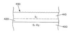
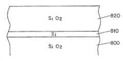
- 제18항에 있어서,상기 비결정질 실리콘 박막 샘플상에 단단한 캡층을 형성하는 단계는 상기 비결정질 실리콘 박막 샘플상에 실리콘 산화층을 형성하는 단계를 포함하는, 비결정질 실리콘 박막 처리 방법.
- 제18항에 있어서,상기 비결정질 실리콘 박막상에 단단한 캡층을 형성하는 단계는 상기 비결정질 실리콘 박막 샘플상에 약 2㎛ 두께의 실리콘 산화층을 형성하는 단계를 포함하는, 비결정질 실리콘 박막 처리 방법.
Applications Claiming Priority (1)
| Application Number | Priority Date | Filing Date | Title |
|---|---|---|---|
| PCT/US2000/007479WO2001071791A1 (en) | 2000-03-21 | 2000-03-21 | Surface planarization of thin silicon films during and after processing by the sequential lateral solidification method |
Publications (2)
| Publication Number | Publication Date |
|---|---|
| KR20020002466A KR20020002466A (ko) | 2002-01-09 |
| KR100672909B1true KR100672909B1 (ko) | 2007-01-22 |
Family
ID=21741175
Family Applications (1)
| Application Number | Title | Priority Date | Filing Date |
|---|---|---|---|
| KR1020017014881AExpired - Fee RelatedKR100672909B1 (ko) | 2000-03-21 | 2000-03-21 | Sls 방법에 의한 처리중 및 처리후의 실리콘 박막의표면 평탄화 |
Country Status (10)
| Country | Link |
|---|---|
| EP (1) | EP1196947A4 (ko) |
| JP (1) | JP4220156B2 (ko) |
| KR (1) | KR100672909B1 (ko) |
| CN (1) | CN1186802C (ko) |
| AU (1) | AU2000240180A1 (ko) |
| CA (1) | CA2374498A1 (ko) |
| HK (1) | HK1046469A1 (ko) |
| MX (1) | MXPA01011852A (ko) |
| TW (1) | TW499717B (ko) |
| WO (1) | WO2001071791A1 (ko) |
Families Citing this family (29)
| Publication number | Priority date | Publication date | Assignee | Title |
|---|---|---|---|---|
| US6555449B1 (en) | 1996-05-28 | 2003-04-29 | Trustees Of Columbia University In The City Of New York | Methods for producing uniform large-grained and grain boundary location manipulated polycrystalline thin film semiconductors using sequential lateral solidfication |
| KR100333275B1 (ko)* | 1999-05-20 | 2002-04-24 | 구본준, 론 위라하디락사 | 액정표시장치의 tft 및 그 제조방법 |
| US7135070B2 (en) | 2002-04-23 | 2006-11-14 | Sharp Laboratories Of America, Inc. | Monolithic stacked/layered crystal-structure-processed mechanical, and combined mechanical and electrical, devices and methods and systems for making |
| US7156916B2 (en) | 2002-04-23 | 2007-01-02 | Sharp Laboratories Of America, Inc. | Monolithic integrated crystal-structure-processed mechanical, and combined mechanical and electrical devices, and methods and systems for making |
| US7125451B2 (en) | 2002-04-23 | 2006-10-24 | Sharp Laboratories Of America, Inc. | Crystal-structure-processed mechanical devices and methods and systems for making |
| US7128783B2 (en) | 2002-04-23 | 2006-10-31 | Sharp Laboratories Of America, Inc. | Thin-film crystal-structure-processed mechanical devices, and methods and systems for making |
| US6860939B2 (en) | 2002-04-23 | 2005-03-01 | Sharp Laboratories Of America, Inc. | Semiconductor crystal-structure-processed mechanical devices, and methods and systems for making |
| WO2004017380A2 (en) | 2002-08-19 | 2004-02-26 | The Trustees Of Columbia University In The City Of New York | A single-shot semiconductor processing system and method having various irradiation patterns |
| KR101131040B1 (ko)* | 2002-08-19 | 2012-03-30 | 더 트러스티스 오브 콜롬비아 유니버시티 인 더 시티 오브 뉴욕 | 에지 영역을 최소화하도록 기판 상의 박막 영역을 레이저결정화 처리하는 방법 및 시스템, 그리고 그러한 박막 영역의 구조 |
| TWI359441B (en) | 2003-09-16 | 2012-03-01 | Univ Columbia | Processes and systems for laser crystallization pr |
| US7364952B2 (en) | 2003-09-16 | 2008-04-29 | The Trustees Of Columbia University In The City Of New York | Systems and methods for processing thin films |
| US7164152B2 (en) | 2003-09-16 | 2007-01-16 | The Trustees Of Columbia University In The City Of New York | Laser-irradiated thin films having variable thickness |
| WO2005029547A2 (en) | 2003-09-16 | 2005-03-31 | The Trustees Of Columbia University In The City Of New York | Enhancing the width of polycrystalline grains with mask |
| US7318866B2 (en) | 2003-09-16 | 2008-01-15 | The Trustees Of Columbia University In The City Of New York | Systems and methods for inducing crystallization of thin films using multiple optical paths |
| WO2005034193A2 (en) | 2003-09-19 | 2005-04-14 | The Trustees Of Columbia University In The City Ofnew York | Single scan irradiation for crystallization of thin films |
| JP2005129769A (ja) | 2003-10-24 | 2005-05-19 | Hitachi Ltd | 半導体薄膜の改質方法、改質した半導体薄膜とその評価方法、およびこの半導体薄膜で形成した薄膜トランジスタ、並びにこの薄膜トランジスタを用いて構成した回路を有する画像表示装置 |
| JP2007165716A (ja) | 2005-12-15 | 2007-06-28 | Advanced Lcd Technologies Development Center Co Ltd | レーザー結晶化装置及び結晶化方法 |
| JP2009032969A (ja)* | 2007-07-27 | 2009-02-12 | Sharp Corp | 半導体薄膜の製造装置、その方法、その方法によって作製された半導体薄膜および半導体素子 |
| TW200942935A (en) | 2007-09-21 | 2009-10-16 | Univ Columbia | Collections of laterally crystallized semiconductor islands for use in thin film transistors and systems and methods for making same |
| WO2009067687A1 (en) | 2007-11-21 | 2009-05-28 | The Trustees Of Columbia University In The City Of New York | Systems and methods for preparation of epitaxially textured thick films |
| US9646831B2 (en) | 2009-11-03 | 2017-05-09 | The Trustees Of Columbia University In The City Of New York | Advanced excimer laser annealing for thin films |
| US9087696B2 (en) | 2009-11-03 | 2015-07-21 | The Trustees Of Columbia University In The City Of New York | Systems and methods for non-periodic pulse partial melt film processing |
| US8440581B2 (en) | 2009-11-24 | 2013-05-14 | The Trustees Of Columbia University In The City Of New York | Systems and methods for non-periodic pulse sequential lateral solidification |
| CN103745925A (zh)* | 2013-11-14 | 2014-04-23 | 上海和辉光电有限公司 | 一种平坦化多晶硅薄膜的制造方法 |
| US20160074968A1 (en)* | 2014-09-11 | 2016-03-17 | Suss Microtec Photonic Systems Inc. | Laser etching system including mask reticle for multi-depth etching |
| TWI577488B (zh)* | 2014-11-17 | 2017-04-11 | 財團法人工業技術研究院 | 表面加工方法 |
| CN104779139A (zh)* | 2015-03-31 | 2015-07-15 | 深超光电(深圳)有限公司 | 半导体薄膜的制造方法及薄膜晶体管的制造方法 |
| CN106298451A (zh)* | 2016-08-18 | 2017-01-04 | 昆山国显光电有限公司 | 激光晶化方法及装置 |
| WO2019146021A1 (ja)* | 2018-01-24 | 2019-08-01 | ギガフォトン株式会社 | レーザ加工方法及びレーザ加工システム |
Citations (2)
| Publication number | Priority date | Publication date | Assignee | Title |
|---|---|---|---|---|
| US5523193A (en)* | 1988-05-31 | 1996-06-04 | Texas Instruments Incorporated | Method and apparatus for patterning and imaging member |
| US5591668A (en)* | 1994-03-14 | 1997-01-07 | Matsushita Electric Industrial Co., Ltd. | Laser annealing method for a semiconductor thin film |
Family Cites Families (11)
| Publication number | Priority date | Publication date | Assignee | Title |
|---|---|---|---|---|
| JP2569711B2 (ja)* | 1988-04-07 | 1997-01-08 | 株式会社ニコン | 露光制御装置及び該装置による露光方法 |
| JPH0433327A (ja)* | 1990-05-30 | 1992-02-04 | Kyocera Corp | 半導体結晶化膜の形成方法 |
| JP2973492B2 (ja)* | 1990-08-22 | 1999-11-08 | ソニー株式会社 | 半導体薄膜の結晶化方法 |
| KR100299292B1 (ko)* | 1993-11-02 | 2001-12-01 | 이데이 노부유끼 | 다결정실리콘박막형성방법및그표면처리장치 |
| US5496768A (en)* | 1993-12-03 | 1996-03-05 | Casio Computer Co., Ltd. | Method of manufacturing polycrystalline silicon thin film |
| JP3326654B2 (ja)* | 1994-05-02 | 2002-09-24 | ソニー株式会社 | 表示用半導体チップの製造方法 |
| TW297138B (ko)* | 1995-05-31 | 1997-02-01 | Handotai Energy Kenkyusho Kk | |
| CA2256699C (en)* | 1996-05-28 | 2003-02-25 | The Trustees Of Columbia University In The City Of New York | Crystallization processing of semiconductor film regions on a substrate, and devices made therewith |
| GB9819338D0 (en)* | 1998-09-04 | 1998-10-28 | Philips Electronics Nv | Laser crystallisation of thin films |
| US6573531B1 (en)* | 1999-09-03 | 2003-06-03 | The Trustees Of Columbia University In The City Of New York | Systems and methods using sequential lateral solidification for producing single or polycrystalline silicon thin films at low temperatures |
| US6368945B1 (en)* | 2000-03-16 | 2002-04-09 | The Trustees Of Columbia University In The City Of New York | Method and system for providing a continuous motion sequential lateral solidification |
- 2000
- 2000-03-21CACA002374498Apatent/CA2374498A1/ennot_activeAbandoned
- 2000-03-21CNCNB008106878Apatent/CN1186802C/zhnot_activeExpired - Fee Related
- 2000-03-21WOPCT/US2000/007479patent/WO2001071791A1/enactiveIP Right Grant
- 2000-03-21HKHK02107913.7Apatent/HK1046469A1/zhunknown
- 2000-03-21EPEP00919501Apatent/EP1196947A4/ennot_activeWithdrawn
- 2000-03-21KRKR1020017014881Apatent/KR100672909B1/konot_activeExpired - Fee Related
- 2000-03-21AUAU2000240180Apatent/AU2000240180A1/ennot_activeAbandoned
- 2000-03-21MXMXPA01011852Apatent/MXPA01011852A/esactiveIP Right Grant
- 2000-03-21JPJP2001569872Apatent/JP4220156B2/janot_activeExpired - Fee Related
- 2001
- 2001-09-12TWTW090122674Apatent/TW499717B/zhnot_activeIP Right Cessation
Patent Citations (2)
| Publication number | Priority date | Publication date | Assignee | Title |
|---|---|---|---|---|
| US5523193A (en)* | 1988-05-31 | 1996-06-04 | Texas Instruments Incorporated | Method and apparatus for patterning and imaging member |
| US5591668A (en)* | 1994-03-14 | 1997-01-07 | Matsushita Electric Industrial Co., Ltd. | Laser annealing method for a semiconductor thin film |
Also Published As
| Publication number | Publication date |
|---|---|
| CN1186802C (zh) | 2005-01-26 |
| AU2000240180A1 (en) | 2001-10-03 |
| CN1363117A (zh) | 2002-08-07 |
| MXPA01011852A (es) | 2002-05-06 |
| CA2374498A1 (en) | 2001-09-27 |
| TW499717B (en) | 2002-08-21 |
| HK1046469A1 (zh) | 2003-01-10 |
| JP2003528463A (ja) | 2003-09-24 |
| WO2001071791A1 (en) | 2001-09-27 |
| EP1196947A1 (en) | 2002-04-17 |
| JP4220156B2 (ja) | 2009-02-04 |
| EP1196947A4 (en) | 2003-08-13 |
| KR20020002466A (ko) | 2002-01-09 |
Similar Documents
| Publication | Publication Date | Title |
|---|---|---|
| KR100672909B1 (ko) | Sls 방법에 의한 처리중 및 처리후의 실리콘 박막의표면 평탄화 | |
| US7220660B2 (en) | Surface planarization of thin silicon films during and after processing by the sequential lateral solidification method | |
| US6368945B1 (en) | Method and system for providing a continuous motion sequential lateral solidification | |
| US6555449B1 (en) | Methods for producing uniform large-grained and grain boundary location manipulated polycrystalline thin film semiconductors using sequential lateral solidfication | |
| JP2007288159A (ja) | 逐次的横方向結晶化法による処理中及び処理後のシリコンフィルムの表面平坦化法 |
Legal Events
| Date | Code | Title | Description |
|---|---|---|---|
| PA0105 | International application | St.27 status event code:A-0-1-A10-A15-nap-PA0105 | |
| PG1501 | Laying open of application | St.27 status event code:A-1-1-Q10-Q12-nap-PG1501 | |
| A201 | Request for examination | ||
| PA0201 | Request for examination | St.27 status event code:A-1-2-D10-D11-exm-PA0201 | |
| E902 | Notification of reason for refusal | ||
| PE0902 | Notice of grounds for rejection | St.27 status event code:A-1-2-D10-D21-exm-PE0902 | |
| P11-X000 | Amendment of application requested | St.27 status event code:A-2-2-P10-P11-nap-X000 | |
| P13-X000 | Application amended | St.27 status event code:A-2-2-P10-P13-nap-X000 | |
| E701 | Decision to grant or registration of patent right | ||
| PE0701 | Decision of registration | St.27 status event code:A-1-2-D10-D22-exm-PE0701 | |
| GRNT | Written decision to grant | ||
| PR0701 | Registration of establishment | St.27 status event code:A-2-4-F10-F11-exm-PR0701 | |
| PR1002 | Payment of registration fee | St.27 status event code:A-2-2-U10-U12-oth-PR1002 Fee payment year number:1 | |
| PG1601 | Publication of registration | St.27 status event code:A-4-4-Q10-Q13-nap-PG1601 | |
| PR1001 | Payment of annual fee | St.27 status event code:A-4-4-U10-U11-oth-PR1001 Fee payment year number:4 | |
| PR1001 | Payment of annual fee | St.27 status event code:A-4-4-U10-U11-oth-PR1001 Fee payment year number:5 | |
| PR1001 | Payment of annual fee | St.27 status event code:A-4-4-U10-U11-oth-PR1001 Fee payment year number:6 | |
| FPAY | Annual fee payment | Payment date:20130108 Year of fee payment:7 | |
| PR1001 | Payment of annual fee | St.27 status event code:A-4-4-U10-U11-oth-PR1001 Fee payment year number:7 | |
| R18-X000 | Changes to party contact information recorded | St.27 status event code:A-5-5-R10-R18-oth-X000 | |
| FPAY | Annual fee payment | Payment date:20140702 Year of fee payment:8 | |
| PR1001 | Payment of annual fee | St.27 status event code:A-4-4-U10-U11-oth-PR1001 Fee payment year number:8 | |
| FPAY | Annual fee payment | Payment date:20150106 Year of fee payment:9 | |
| PR1001 | Payment of annual fee | St.27 status event code:A-4-4-U10-U11-oth-PR1001 Fee payment year number:9 | |
| FPAY | Annual fee payment | Payment date:20160621 Year of fee payment:10 | |
| PR1001 | Payment of annual fee | St.27 status event code:A-4-4-U10-U11-oth-PR1001 Fee payment year number:10 | |
| PR1001 | Payment of annual fee | St.27 status event code:A-4-4-U10-U11-oth-PR1001 Fee payment year number:11 | |
| LAPS | Lapse due to unpaid annual fee | ||
| PC1903 | Unpaid annual fee | St.27 status event code:A-4-4-U10-U13-oth-PC1903 Not in force date:20180117 Payment event data comment text:Termination Category : DEFAULT_OF_REGISTRATION_FEE | |
| PC1903 | Unpaid annual fee | St.27 status event code:N-4-6-H10-H13-oth-PC1903 Ip right cessation event data comment text:Termination Category : DEFAULT_OF_REGISTRATION_FEE Not in force date:20180117 |