KR100672628B1 - Active Matrix Organic Electroluminescent Display Device - Google Patents
Active Matrix Organic Electroluminescent Display DeviceDownload PDFInfo
- Publication number
- KR100672628B1 KR100672628B1KR1020000085560AKR20000085560AKR100672628B1KR 100672628 B1KR100672628 B1KR 100672628B1KR 1020000085560 AKR1020000085560 AKR 1020000085560AKR 20000085560 AKR20000085560 AKR 20000085560AKR 100672628 B1KR100672628 B1KR 100672628B1
- Authority
- KR
- South Korea
- Prior art keywords
- sls
- line
- data
- scan
- active matrix
- Prior art date
- Legal status (The legal status is an assumption and is not a legal conclusion. Google has not performed a legal analysis and makes no representation as to the accuracy of the status listed.)
- Expired - Lifetime
Links
- 239000011159matrix materialSubstances0.000titleclaimsabstractdescription25
- 238000000034methodMethods0.000claimsabstractdescription46
- 239000000758substrateSubstances0.000claimsabstractdescription18
- 229910021420polycrystalline siliconInorganic materials0.000claimsdescription12
- 238000007711solidificationMethods0.000claimsdescription8
- 230000008023solidificationEffects0.000claimsdescription8
- 239000003990capacitorSubstances0.000claimsdescription3
- 230000010354integrationEffects0.000abstract1
- 229910052710siliconInorganic materials0.000abstract1
- 239000010703siliconSubstances0.000abstract1
- 239000010409thin filmSubstances0.000abstract1
- 239000010410layerSubstances0.000description28
- 239000004065semiconductorSubstances0.000description17
- 239000013078crystalSubstances0.000description5
- 238000004519manufacturing processMethods0.000description5
- 238000010586diagramMethods0.000description3
- 239000002184metalSubstances0.000description3
- 229910052739hydrogenInorganic materials0.000description2
- 239000001257hydrogenSubstances0.000description2
- 125000004435hydrogen atomChemical group[H]*0.000description2
- 238000002347injectionMethods0.000description2
- 239000007924injectionSubstances0.000description2
- 239000011229interlayerSubstances0.000description2
- 238000002161passivationMethods0.000description2
- 230000001681protective effectEffects0.000description2
- 230000002950deficientEffects0.000description1
- 230000005684electric fieldEffects0.000description1
- 238000005401electroluminescenceMethods0.000description1
- 230000005525hole transportEffects0.000description1
- 238000012986modificationMethods0.000description1
- 230000004048modificationEffects0.000description1
Images


Classifications
- G—PHYSICS
- G09—EDUCATION; CRYPTOGRAPHY; DISPLAY; ADVERTISING; SEALS
- G09G—ARRANGEMENTS OR CIRCUITS FOR CONTROL OF INDICATING DEVICES USING STATIC MEANS TO PRESENT VARIABLE INFORMATION
- G09G3/00—Control arrangements or circuits, of interest only in connection with visual indicators other than cathode-ray tubes
- G09G3/20—Control arrangements or circuits, of interest only in connection with visual indicators other than cathode-ray tubes for presentation of an assembly of a number of characters, e.g. a page, by composing the assembly by combination of individual elements arranged in a matrix no fixed position being assigned to or needed to be assigned to the individual characters or partial characters
- G09G3/22—Control arrangements or circuits, of interest only in connection with visual indicators other than cathode-ray tubes for presentation of an assembly of a number of characters, e.g. a page, by composing the assembly by combination of individual elements arranged in a matrix no fixed position being assigned to or needed to be assigned to the individual characters or partial characters using controlled light sources
- G09G3/30—Control arrangements or circuits, of interest only in connection with visual indicators other than cathode-ray tubes for presentation of an assembly of a number of characters, e.g. a page, by composing the assembly by combination of individual elements arranged in a matrix no fixed position being assigned to or needed to be assigned to the individual characters or partial characters using controlled light sources using electroluminescent panels
- G09G3/32—Control arrangements or circuits, of interest only in connection with visual indicators other than cathode-ray tubes for presentation of an assembly of a number of characters, e.g. a page, by composing the assembly by combination of individual elements arranged in a matrix no fixed position being assigned to or needed to be assigned to the individual characters or partial characters using controlled light sources using electroluminescent panels semiconductive, e.g. using light-emitting diodes [LED]
- G09G3/3208—Control arrangements or circuits, of interest only in connection with visual indicators other than cathode-ray tubes for presentation of an assembly of a number of characters, e.g. a page, by composing the assembly by combination of individual elements arranged in a matrix no fixed position being assigned to or needed to be assigned to the individual characters or partial characters using controlled light sources using electroluminescent panels semiconductive, e.g. using light-emitting diodes [LED] organic, e.g. using organic light-emitting diodes [OLED]
- G09G3/3225—Control arrangements or circuits, of interest only in connection with visual indicators other than cathode-ray tubes for presentation of an assembly of a number of characters, e.g. a page, by composing the assembly by combination of individual elements arranged in a matrix no fixed position being assigned to or needed to be assigned to the individual characters or partial characters using controlled light sources using electroluminescent panels semiconductive, e.g. using light-emitting diodes [LED] organic, e.g. using organic light-emitting diodes [OLED] using an active matrix
- G09G3/3233—Control arrangements or circuits, of interest only in connection with visual indicators other than cathode-ray tubes for presentation of an assembly of a number of characters, e.g. a page, by composing the assembly by combination of individual elements arranged in a matrix no fixed position being assigned to or needed to be assigned to the individual characters or partial characters using controlled light sources using electroluminescent panels semiconductive, e.g. using light-emitting diodes [LED] organic, e.g. using organic light-emitting diodes [OLED] using an active matrix with pixel circuitry controlling the current through the light-emitting element
- H—ELECTRICITY
- H01—ELECTRIC ELEMENTS
- H01L—SEMICONDUCTOR DEVICES NOT COVERED BY CLASS H10
- H01L21/00—Processes or apparatus adapted for the manufacture or treatment of semiconductor or solid state devices or of parts thereof
- H01L21/02—Manufacture or treatment of semiconductor devices or of parts thereof
- H01L21/02104—Forming layers
- H01L21/02365—Forming inorganic semiconducting materials on a substrate
- H01L21/02518—Deposited layers
- H01L21/02521—Materials
- H01L21/02524—Group 14 semiconducting materials
- H01L21/02532—Silicon, silicon germanium, germanium
- H—ELECTRICITY
- H01—ELECTRIC ELEMENTS
- H01L—SEMICONDUCTOR DEVICES NOT COVERED BY CLASS H10
- H01L21/00—Processes or apparatus adapted for the manufacture or treatment of semiconductor or solid state devices or of parts thereof
- H01L21/02—Manufacture or treatment of semiconductor devices or of parts thereof
- H01L21/02104—Forming layers
- H01L21/02365—Forming inorganic semiconducting materials on a substrate
- H01L21/02518—Deposited layers
- H01L21/02587—Structure
- H01L21/0259—Microstructure
- H01L21/02595—Microstructure polycrystalline
- H—ELECTRICITY
- H01—ELECTRIC ELEMENTS
- H01L—SEMICONDUCTOR DEVICES NOT COVERED BY CLASS H10
- H01L21/00—Processes or apparatus adapted for the manufacture or treatment of semiconductor or solid state devices or of parts thereof
- H01L21/02—Manufacture or treatment of semiconductor devices or of parts thereof
- H01L21/02104—Forming layers
- H01L21/02365—Forming inorganic semiconducting materials on a substrate
- H01L21/02656—Special treatments
- H01L21/02664—Aftertreatments
- H01L21/02667—Crystallisation or recrystallisation of non-monocrystalline semiconductor materials, e.g. regrowth
- H01L21/02675—Crystallisation or recrystallisation of non-monocrystalline semiconductor materials, e.g. regrowth using laser beams
- H01L21/02686—Pulsed laser beam
- H—ELECTRICITY
- H01—ELECTRIC ELEMENTS
- H01L—SEMICONDUCTOR DEVICES NOT COVERED BY CLASS H10
- H01L21/00—Processes or apparatus adapted for the manufacture or treatment of semiconductor or solid state devices or of parts thereof
- H01L21/02—Manufacture or treatment of semiconductor devices or of parts thereof
- H01L21/02104—Forming layers
- H01L21/02365—Forming inorganic semiconducting materials on a substrate
- H01L21/02656—Special treatments
- H01L21/02664—Aftertreatments
- H01L21/02667—Crystallisation or recrystallisation of non-monocrystalline semiconductor materials, e.g. regrowth
- H01L21/02691—Scanning of a beam
- H—ELECTRICITY
- H10—SEMICONDUCTOR DEVICES; ELECTRIC SOLID-STATE DEVICES NOT OTHERWISE PROVIDED FOR
- H10D—INORGANIC ELECTRIC SEMICONDUCTOR DEVICES
- H10D86/00—Integrated devices formed in or on insulating or conducting substrates, e.g. formed in silicon-on-insulator [SOI] substrates or on stainless steel or glass substrates
- H10D86/01—Manufacture or treatment
- H10D86/021—Manufacture or treatment of multiple TFTs
- H10D86/0221—Manufacture or treatment of multiple TFTs comprising manufacture, treatment or patterning of TFT semiconductor bodies
- H10D86/0223—Manufacture or treatment of multiple TFTs comprising manufacture, treatment or patterning of TFT semiconductor bodies comprising crystallisation of amorphous, microcrystalline or polycrystalline semiconductor materials
- H10D86/0229—Manufacture or treatment of multiple TFTs comprising manufacture, treatment or patterning of TFT semiconductor bodies comprising crystallisation of amorphous, microcrystalline or polycrystalline semiconductor materials characterised by control of the annealing or irradiation parameters
- G—PHYSICS
- G09—EDUCATION; CRYPTOGRAPHY; DISPLAY; ADVERTISING; SEALS
- G09G—ARRANGEMENTS OR CIRCUITS FOR CONTROL OF INDICATING DEVICES USING STATIC MEANS TO PRESENT VARIABLE INFORMATION
- G09G2300/00—Aspects of the constitution of display devices
- G09G2300/04—Structural and physical details of display devices
- G09G2300/0404—Matrix technologies
- G09G2300/0408—Integration of the drivers onto the display substrate
- G—PHYSICS
- G09—EDUCATION; CRYPTOGRAPHY; DISPLAY; ADVERTISING; SEALS
- G09G—ARRANGEMENTS OR CIRCUITS FOR CONTROL OF INDICATING DEVICES USING STATIC MEANS TO PRESENT VARIABLE INFORMATION
- G09G2300/00—Aspects of the constitution of display devices
- G09G2300/08—Active matrix structure, i.e. with use of active elements, inclusive of non-linear two terminal elements, in the pixels together with light emitting or modulating elements
- G09G2300/0809—Several active elements per pixel in active matrix panels
- G09G2300/0842—Several active elements per pixel in active matrix panels forming a memory circuit, e.g. a dynamic memory with one capacitor
- H—ELECTRICITY
- H10—SEMICONDUCTOR DEVICES; ELECTRIC SOLID-STATE DEVICES NOT OTHERWISE PROVIDED FOR
- H10K—ORGANIC ELECTRIC SOLID-STATE DEVICES
- H10K59/00—Integrated devices, or assemblies of multiple devices, comprising at least one organic light-emitting element covered by group H10K50/00
- H10K59/10—OLED displays
- H10K59/12—Active-matrix OLED [AMOLED] displays
- H10K59/121—Active-matrix OLED [AMOLED] displays characterised by the geometry or disposition of pixel elements
- H10K59/1213—Active-matrix OLED [AMOLED] displays characterised by the geometry or disposition of pixel elements the pixel elements being TFTs
Landscapes
- Engineering & Computer Science (AREA)
- Physics & Mathematics (AREA)
- Computer Hardware Design (AREA)
- General Physics & Mathematics (AREA)
- Microelectronics & Electronic Packaging (AREA)
- Condensed Matter Physics & Semiconductors (AREA)
- Manufacturing & Machinery (AREA)
- Power Engineering (AREA)
- Crystallography & Structural Chemistry (AREA)
- Chemical & Material Sciences (AREA)
- Optics & Photonics (AREA)
- Theoretical Computer Science (AREA)
- Electroluminescent Light Sources (AREA)
- Thin Film Transistor (AREA)
- Devices For Indicating Variable Information By Combining Individual Elements (AREA)
Abstract
Translated fromKoreanDescription
Translated fromKorean도1은 액티브 매티릭스 유기 전계발광 디스플레이 장치의 간략한 레이아웃도1 is a simplified layout diagram of an active matrix organic electroluminescent display device
도2는 상기 도1의 액티브 매트릭스 유기 전계발광 디스플레이 장치의 하나의 화소를 도시한 도면FIG. 2 illustrates one pixel of the active matrix organic electroluminescent display device of FIG.
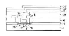
도3은 구동부(T) 중 유기EL소자(P)와 연결되는 트랜지스터_P0와의 콘택 단면도FIG. 3 is a cross-sectional view of a contact between the driving unit T and the transistor _P0 connected to the organic EL device P. FIG.
도4a는 본발명에 따른 제1실시예로, 화소부(다수개의 화소로 구성)의 TFT에 SLS(연속 측면 결정)방식을 적용한 도면.Fig. 4A is a view of applying a SLS (continuous side determination) method to a TFT of a pixel portion (comprising of a plurality of pixels) in a first embodiment according to the present invention.
도4b는 본발명에 따른 제2실시예로, 화소부(다수개의 화소로 구성)를 구동하기 위한 구동회로의 TFT를 SLS(연속 측면 결정)방식을 적용한 도면.Fig. 4B is a view of applying a SLS (continuous side determination) method to a TFT of a driving circuit for driving a pixel portion (consisting of a plurality of pixels) in a second embodiment according to the present invention.
*도면의 주요부분에 대한 부호의 설명* Explanation of symbols for main parts of the drawings
1 : 투명기판 2 : 반도체층1: transparent substrate 2: semiconductor layer
3 : 도핑영역 4 :게이트 절연막3: doped region 4: gate insulating film
5 : 게이트 전극 6 : 층간절연막5
7 : 소스 전극 8 : 드레인 전극7
10 : 보호막 11 : 화소전극10: protective film 11: pixel electrode
13 : 유기EL층 14 : 메탈전극13
본 발명은 액티브 매트릭스 유기 전계발광 디스플레이 장치에 관한 것으로, 특히 SLS(sequential lateral solidification)법을 사용하여 기존의 저온 폴리공정보다 휘도의 균일성이 높고 회로의 집적화가 가능한 액티브 매트릭스 전계 발광 디스플레이 장치에 관한 것이다.BACKGROUND OF THE
최근 평판 디스플레이의 발전에 따라 LCD, PDP, FED, EL 등 여러 종류의 디스플레이 소자들이 개발되고 있다. 이러한 평판 디스플레이는 그 구동 방법에 따라 다음과 같이 크게 두 가지로 나눌 수 있다.Recently, with the development of flat panel displays, various types of display devices such as LCD, PDP, FED, and EL have been developed. Such a flat panel display can be divided into two types according to its driving method as follows.
그 중 하나는 패시브 매트릭스(Passive Matrix) 방식이고, 또 다른 하나는 액티브 매트릭스(Active Matrix)방식이다. 패시브 매트릭스 방식은 액티브 매트릭스 방식에 비해 더욱 큰 전류 레벨을 요구한다.One of them is a passive matrix method, the other is an active matrix method. Passive matrix schemes require greater current levels than active matrix schemes.
따라서 FED 나 EL 등과 같은 전류 구동 방식에서는 동일한 라인 타임(Line Time)이라도 더욱 큰 전류 레벨을 요구하는 패시브 매트릭스 방식보다 액티브 매트릭스 방식이 보다 유리한 방식으로 인식되고 있다.Therefore, in the current driving method such as FED or EL, the active matrix method is recognized as more advantageous than the passive matrix method requiring a larger current level even at the same line time.
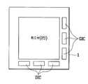
도1은 액티브 매티릭스 유기 전계발광 디스플레이 장치의 간략한 레이아웃도이다.1 is a simplified layout diagram of an active matrix organic electroluminescent display device.
도1에 도시한 바와 같이 스캔신호가 차례로 인가되는 다수 개의 스캔라인(S) 과, 상기 스캔라인(S)과 교차하게 다수 개로 배치되고 데이터신호를 인가하는 데이터라인(D)과, 상기 스캔라인(S)과 데이터라인(D)에 의해 정의되는 화소가 형성되어 있으며, 상기 화소는 발광하는 영역인 유기EL소자(P)와, 상기 스캔라인(S) 및 데이터라인(D)과, 상기 유기EL소자(P)와 연결되어 상기 유기EL소자(P)를 구동시키기 위한 구동부(T)로 구성되어 있다.As shown in FIG. 1, a plurality of scan lines S to which scan signals are sequentially applied, a plurality of scan lines S arranged to cross the scan lines S, and a data line D to which data signals are applied, and the scan lines A pixel defined by S and a data line D is formed, and the pixel is an organic EL element P which emits light, the scan line S and the data line D, and the organic light. It is composed of a drive unit T connected to the EL element P to drive the organic EL element P.
도2는 상기 도1의 액티브 매트릭스 유기 전계발광 디스플레이 장치의 하나의 화소를 도시한 것으로, 상기 각 화소에는 유기EL소자(P) 중 OLED(organic light emitting device : P)와, 2개의 TFT로 형성되어 상기 OLED(P)를 구동하기 위한 전류를 공급하는 구동부(T)가 형성된다.FIG. 2 shows one pixel of the active matrix organic electroluminescent display device of FIG. 1, wherein each pixel is formed of an organic light emitting device (P) among organic EL elements P and two TFTs. As a result, a driver T for supplying a current for driving the OLED P is formed.
상기와 같은 스위치_P1과 트랜지스터_P0는 TFT로 투명기판의 상부에 각각의 반도체층이 형성되는데, 상기 반도체층은 Si를 기판상부에 형성하고 엑시머 레이저(Excimer laser)를 이용하여 스캐닝방식을 채택하여 Si를 결정화시켜 폴리 Si를 얻는 방법을 이용하였다.As described above, each of the switches _P1 and the transistor _P0 is a TFT, and each semiconductor layer is formed on the transparent substrate. The semiconductor layer forms Si on the substrate and adopts a scanning method using an excimer laser. To crystallize Si to obtain poly Si.
그리고 상기 반도체층의 Si는 수소(H)가 소정 퍼센트 결합되어 있어, 상기 수소를 제거하기 위한 최소한의 온도를 유지하며, 상기 반도체층의 형성시 투명기판이 변형이 없도록 저온을 유지하여 LTPS를 형성해야 한다.In addition, since Si of the semiconductor layer is hydrogen (H) bonded to a predetermined percentage, it maintains a minimum temperature for removing the hydrogen, and maintains a low temperature so that the transparent substrate does not deform when forming the semiconductor layer to form LTPS. Should be.
그러나 상기의 방식은 스캐닝라인 당 소정 펄스를 인가하는 방식으로 레이져가 연속적으로 조사되지 않고, 또한 각 라인당 조사되는 양이 균일하지 않다. 이는 스캐닝방향으로 줄무늬를 형성시키고, 상기 줄무늬에 의해 스캐닝라인당 TFT의 특성이 불균일하게 되어 유기전계발광소자의 디스플레이 화면의 줄무늬로 반영되어 휘도의 불균일도에 영향을 준다.However, in the above method, the laser is not irradiated continuously by applying a predetermined pulse per scanning line, and the amount irradiated per line is not uniform. This results in streaks in the scanning direction, and the streaks cause non-uniformity of TFTs per scanning line, which is reflected as streaks on the display screen of the organic light emitting display device, thereby affecting the unevenness of luminance.
즉, 전류의 통로인 채널의 역할을 하는 반도체층을 이루는 Si 그레인의 크기 및 결정상태가 불균일하게 되므로 각 화소를 구동하는 TFT의 특성이 달라져 같은 그레이 레벨을 인가하여도 각 TFT에 흐르는 전류의 양이 달라지고, 이는 화소의 휘도에 차이를 가져온다.That is, since the size and crystal state of the Si grains forming the semiconductor layer serving as the channel, which is a path for current, become uneven, the characteristics of the TFTs driving the respective pixels are different and the amount of current flowing through each TFT even when the same gray level is applied. Is different, which brings a difference in the luminance of the pixel.
또한 Si의 그레인(grain)의 크기가 일정하지 않아 그레인의 경계면에서 돌출부에 의해 TFT 제작시 특성의 불균일을 야기시켜 휘도의 불균일도에 영향을 준다.In addition, the size of the grain (grain) of Si is not constant, which causes non-uniformity of characteristics during TFT fabrication due to protrusions at the interface of the grains, thereby affecting the unevenness of luminance.
이상에서 설명한 종래 기술에 따른 액티브 매트릭스 유기 전계발광 디스플레이 장치는 다음과 같은 문제점이 있다.The active matrix organic electroluminescent display device according to the related art described above has the following problems.
엑시머 레이저를 이용한 스캐닝방식에 의한 폴리-Si로 제작한 TFT를 유기전계발광소자의 구동소자로 사용할 경우 휘도의 불균일한 원인으로 작용한다.When TFTs made of poly-Si by a scanning method using an excimer laser are used as driving elements of an organic light emitting device, they act as a non-uniform cause of luminance.
또한 상기의 휘도의 불균일을 회로적으로 보상하기 위해 화소부에 TFT를 4개 사용하는 보상회로기술이 있지만 이 기술은 제조공정상 불량율을 증가시킬 수 있고 TFT이 숫자가 증가함으로 인하여 개구율을 감소시키는 단점이 있다.In addition, there is a compensation circuit technique using four TFTs in the pixel portion to compensate for the above-mentioned luminance unevenness, but this technique can increase the defective rate in the manufacturing process and reduce the aperture ratio due to the increase in the number of TFTs. There is this.
따라서 본 발명은 상기와 같은 문제점을 해결하기 위해 안출한 것으로서, 유기EL소자를 구동하기 위한 구동부의 TFT 및/또는 구동부와 연결된 드라이브IC이 TFT를 SLS(Sequential Lateral Solidification) 방식으로 제조하여 TFT의 특성의 균일도를 높여 균일 휘도를 가지고, 따라서 적은 수의 트랜지스터를 이용하여 고개구율을 갖는 액티브 매트릭스 유기 전계발광 디스플레이 장치를 제공하는데 그 목 적이 있다.Therefore, the present invention has been made to solve the above problems, the TFT of the driving unit for driving the organic EL device and / or the drive IC connected to the driving unit by manufacturing the TFT in the SLS (Sequential Lateral Solidification) method, the characteristics of the TFT The purpose of the present invention is to provide an active matrix organic electroluminescent display device having a uniform luminance by increasing the uniformity of Hg and thus having a high opening ratio using a small number of transistors.
또한 상기 드라이버IC(외부 구동회로)의 TFT를 SLS 방식으로 제조하여 한 기판에 화소와 구동회로를 집적화하여 소형화된 액티브 매트릭스 유기 전계발광 디스플레이 장치를 제공하는데 그 목적이 있다.In addition, an object of the present invention is to provide an active matrix organic electroluminescent display device which is miniaturized by manufacturing a TFT of the driver IC (external driving circuit) by the SLS method and integrating a pixel and a driving circuit on a substrate.
상기와 같은 목적을 달성하기 위한 본 발명에 따른 액티브 매트릭스 유기 전계발광 디스플레이 장치의 특징은 기판상에 일 방향으로 배열되는 다수 개의 스캔 라인과, 상기 스캔 라인에 수직한 방향으로 배열되는 다수개의 데이터 라인과, 상기 데이터 라인과 일정 거리를 갖고 상기 데이터 라인에 평행한 방향으로 배열되는 파워 라인과, 상기 스캔 라인, 데이터 라인 및 파워 라인 사이의 화소 영역에 형성되어 인가되는 전압에 따라 빛을 발광하는 전계 발광 소자와, 상기 스캔 라인의 신호에 따라 상기 데이터 라인이 신호를 스위칭하는 스위칭 트랜지스터와, 상기 스위칭 트랜지스터를 통해 인가되는 신호에 따라 상기 파워 라인의 전원을 상기 전계 발광 소자에 인가하기 위한 구동 트랜지스터를 구비하며, 상기 스위칭 트랜지스터 또는 구동 트랜지스터가 연속 측면 결정(SLS) 방식에 의해 형성됨을 특징으로 한다.An active matrix organic electroluminescent display device according to the present invention for achieving the above object is a plurality of scan lines arranged in one direction on the substrate, and a plurality of data lines arranged in a direction perpendicular to the scan line And an electric field that emits light according to a voltage applied to a power line formed at a pixel area between the scan line, the data line, and the power line at a predetermined distance from the data line and arranged in a direction parallel to the data line. A light emitting device, a switching transistor in which the data line switches a signal according to a signal of the scan line, and a driving transistor for applying power of the power line to the electroluminescent device in accordance with a signal applied through the switching transistor. And the switching transistor or driving transistor Site is characterized by formed by a continuous lateral crystal (SLS) method.
삭제delete
본 발명의 특징에 따른 작용은 화소영역에 형성된 유기EL소자를 구동하기 위한 구동부의 TFT와, 상기 구동부의 TFT를 구동하기 위한 드라이버IC의 TFT중 적어도 어느 하나를 SLS방식을 이용하여 그레인의 크기 및 결정상태의 균일도가 높은 폴리 Si 결정을 형성하기 때문에 TFT의 특성의 균일도가 높아져 TFT에 의해 구동되는 액티브 매트릭스 유기 전계발광 디스플레이 장치의 각 화소의 휘도 특성의 균일도가 높아진다.According to an aspect of the present invention, at least one of the TFT of the driver for driving the organic EL element formed in the pixel region and the TFT of the driver IC for driving the TFT of the driver is obtained by using the SLS method. Since the poly Si crystal with high uniformity in the crystal state is formed, the uniformity of the characteristics of the TFT is increased, and the uniformity of the luminance characteristic of each pixel of the active matrix organic electroluminescent display device driven by the TFT is increased.
본 발명의 다른 목적, 특성 및 잇점들은 첨부한 도면을 참조한 실시예들의 상세한 설명을 통해 명백해질 것이다.Other objects, features and advantages of the present invention will become apparent from the following detailed description of embodiments taken in conjunction with the accompanying drawings.
본 발명에 따른 액티브 매트릭스 유기 전계발광 디스플레이 장치의 바람직한 실시예에 대하여 첨부한 도면을 참조하여 설명하면 다음과 같다.A preferred embodiment of an active matrix organic electroluminescent display device according to the present invention will be described with reference to the accompanying drawings.
도1은 액티브 매티릭스 유기 전계발광 디스플레이 장치의 간략한 레이아웃도이다.1 is a simplified layout diagram of an active matrix organic electroluminescent display device.
도1에 도시한 바와 같이 스캔신호가 차례로 인가되는 다수 개의 스캔라인(S)과, 상기 스캔라인(S)과 교차하게 다수 개로 배치되고 데이터신호를 인가하는 데이터라인(D)과, 상기 스캔라인(S)과 데이터라인(D)에 의해 정의되는 화소가 형성되어 있으며, 상기 화소는 발광하는 영역인 유기EL소자(P)와, 상기 스캔라인(S) 및 데이터라인(D)과, 상기 유기EL소자(P)와 연결되어 상기 유기EL소자(P)를 구동시키기 위한 구동부(T)로 구성되어 있다.As shown in FIG. 1, a plurality of scan lines S to which scan signals are sequentially applied, a plurality of data lines D arranged to intersect the scan lines S, and to apply a data signal, and the scan lines A pixel defined by S and a data line D is formed, and the pixel is an organic EL element P which emits light, the scan line S and the data line D, and the organic light. It is composed of a drive unit T connected to the EL element P to drive the organic EL element P.
도2는 상기 도1의 액티브 매트릭스 유기 전계발광 디스플레이 장치의 하나의 화소를 도시한 것으로, 상기 각 화소에는 유기EL소자(P) 중 OLED(organic light emitting device : P)와, 2개의 TFT로 형성되어 상기 OLED(P)를 구동하기 위한 전류를 공급하는 구동부(T)가 형성된다.FIG. 2 shows one pixel of the active matrix organic electroluminescent display device of FIG. 1, wherein each pixel is formed of an organic light emitting device (P) among organic EL elements P and two TFTs. As a result, a driver T for supplying a current for driving the OLED P is formed.
즉, 도2에 도시한 바와 같이 구동할 화소를 선택하는 스캔라인(S : Scan Line )과, 제어된 양에 따라 화소에 전압을 인가하는 데이터라인(D :Data Line )과, 상기 스캔라인의 신호에 따라 데이터의 흐름을 제어하는 액티브 소자인 스위치_P1과, 전원을 공급하는 파워라인(P/L: Power Line)과, 상기 데이터라인으로 인가되는 전압에 따라 상기 전압과 상기 파워라인에 의해 공급되는 전압차 만큼의 전하를 축적하는 캐패시터_Cs와, 캐패시터_Cs에 축적된 전하에 의한 전압을 입력받아 전류를 흘려주는 트랜지스터_PO로 구성된 구동부(T)와, 상기 구동용 트랜지스터_PO에 흐르는 전류에 의해 발광하는 OLED(organic light emitting device : P)로 구성되어 있다.That is, as shown in Fig. 2, a scan line (S: Scan Line) for selecting a pixel to drive, a data line (D: Data Line) for applying a voltage to the pixel according to a controlled amount, and Switch _P1, which is an active element that controls the flow of data according to a signal, a power line (P / L) for supplying power, and the voltage and the power line according to a voltage applied to the data line. A driving unit T composed of a capacitor _Cs that accumulates a charge corresponding to the voltage difference supplied, a transistor _PO that receives a voltage from the charge accumulated in the capacitor _Cs and flows a current, and the driving transistor PO It consists of an organic light emitting device (P) which emits light by the electric current which flows.
상기의 2개의 TFT 중 트랜지스터_PO는 도3에 도시한 바와 같이, 투명기판(1) 상에 형성된 반도체층(2), 반도체층(2) 양 주변에 형성된 도핑영역(3), 상기 반도체층(2) 상부에 형성된 게이트 절연막(4), 게이트 절연막(4) 상부에 형성된 게이트 전극(5), 상기 도핑영역(3)이 노출되도록 상기 투명기판(1) 상부에 형성된 층간절 연막(6), 상기 도핑영역(3)과 연결되어 각각 형성된 소스 전극(7)및 드레인 전극(8), 상기 드레인 전극(8)이 노출되도록 비아홀을 갖고 상기 소스/드레인 전극(7, 8)을 포함한 전면에 형성된 보호막(10) 등으로 구성된다.As shown in FIG. 3, the transistor _PO of the two TFTs includes the
그리고 상기 드레인 전극(8)과 연결되도록 상기 보호막(10) 상부 소정영역에 형성된 화소전극(11), 상기 보호막(10) 및 화소전극(11) 상부에 형성된 유기EL층(13), 상기 유기EL층(Electroluminescence layer: 13) 상부에 형성된 메탈전극(14)을 포함하여 구성된 OLED(P)가 형성되어 있다.The
상기 OLED(P)는 유기EL소자 중 하나로, 상기 유기EL소자는 정공 주입층(hole injection layer), 정공 수송층(hole transport layer), 발광층(emmiting layer) 및 전자 수송층(electron transport layer)이 적층되어 형성되어 있다. 그리고 정공 주입층(hole injection layer) 하부에 화소전극(11)과, 전자 수송층 상부에 메탈전극(14)이 형성된다.The OLED (P) is one of the organic EL devices, and the organic EL device includes a hole injection layer, a hole transport layer, an emitting layer, and an electron transport layer. Formed. The
그리고 도시하지 않았지만, 상기 스위치_P1은 상기 트랜지스터_P0의 게이터 전극(5)과 드레인 전극이 연결되고, 게이트전극 및 소스전극이 각각 스캔라인 및 데이터라인에 연결되어 형성된다.Although not illustrated, the switch _ P1 is formed by connecting the
상기와 같은 스위치_P1과 트랜지스터_P0는 TFT로 투명기판(1)의 상부에 각각의 반도체층이 형성되는데, 상기 반도체층은 Si를 기판상부에 형성하고 SLS를 이용하여 Si를 결정화시켜 폴리 Si를 얻는 방법을 이용하였다.As described above, each of the switches _P1 and the transistor _P0 is a TFT, and each semiconductor layer is formed on the
상기 SLS방식은 전류의 통로인 채널의 역할을 하는 반도체층을 이루는 Si 그레인의 크기 및 결정상태의 균일도가 커지므로 각 화소를 구동하는 TFT의 특성이 유사하여 같은 그레이 레벨을 인가시에 각 TFT에 흐르는 전류의 양이 거의 균일하게 되어 이는 화소의 휘도에 차이를 감소시킨다.In the SLS method, the size of Si grains and the uniformity of crystal states of a semiconductor layer serving as a channel serving as a channel of current increase, so that the characteristics of the TFTs driving each pixel are similar to each other when applying the same gray level. The amount of current flowing becomes nearly uniform, which reduces the difference in the luminance of the pixels.
또한 Si의 그레인(grain)의 크기가 일정하게 되어 그레인의 경계면에서 돌출부에 의해 TFT 제작시 특성의 불균일을 방지한다.In addition, the grain size of the Si becomes constant to prevent non-uniformity of characteristics during TFT fabrication by protrusions at the grain boundaries.
도4a는 본발명에 따른 제1실시예로, 화소부(다수개의 화소로 구성)의 TFT에 SLS(연속 측면 결정)방식을 적용한 도면이다.Fig. 4A is a view of applying the SLS (Continuous Side Determination) method to the TFT of the pixel portion (comprising of a plurality of pixels) in the first embodiment according to the present invention.
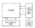
도4a에 도시한 바와 같이, 각 화소(P : 도시하지 않음)로 구성된 화소부와(PS), 상기 화소부(PS)를 구동하기 위한 외부 구동회로가 집적화된 게이트 드라이브 IC(GIC) 및 데이터 드라이브 IC(DIC)와, 데이터 드라이브 IC에 인가되는 데이터신호의 인가시기를 콘트롤하는 타이밍 콘트롤러로 구성된다.As shown in Fig. 4A, a pixel portion PS including each pixel P (not shown), a gate drive IC GIC and data in which an external driving circuit for driving the pixel portion PS is integrated. And a timing controller for controlling the application timing of the data signal applied to the data drive IC.
각 화소(P : 도시하지 않음)를 구동하는 각 구동부(T)의 TFT의 반도체층은 SLS방식으로 형성되고, 상기 게이트 드라이브 IC 및 데이터 드라이브 IC의 TFT의 반도체층은 LTPS 저온공정 및 엑시머 레이저 방식(스캐닝방식), 연속 측면 결정(SLS : sequential lateral solidification) 방식 중 어느 하나를 이용하여 형성된다.The semiconductor layer of the TFT of each driver T driving each pixel P (not shown) is formed by the SLS method, and the semiconductor layer of the TFT of the gate drive IC and the data drive IC is an LTPS low temperature process and an excimer laser method. (Scanning method) or sequential lateral solidification (SLS) method.
도4b는 본발명에 따른 제2실시예로, 화소부(다수개의 화소로 구성)를 구동하기 위한 구동회로의 TFT를 SLS(연속 측면 결정)방식을 적용한 도면이다.Fig. 4B is a view of applying a SLS (continuous side determination) method to a TFT of a driving circuit for driving a pixel portion (consisting of a plurality of pixels) in a second embodiment according to the present invention.
도4b에 도시한 바와 같이, 기판(1) 상에 각 화소(P ; 도시하지 않음)들로 구성된 화소부(PS)와, 상기 화소부(PS)를 구동하기 위해 상기 기판(1) 상에 집적화된 게이트 드라이브 IC(GIC) 및 데이터 드라이브 IC(DIC)와, 데이터 드라이브 IC에 인 가되는 데이터신호의 인가시기를 콘트롤하는 타이밍 콘트롤러로 구성된다.As shown in Fig. 4B, the pixel portion PS composed of the pixels P (not shown) on the
각 화소(P : 도시하지 않음)를 구동하는 각 구동부(T)의 TFT의 반도체층은 LTPS 저온공정 및 엑시머 레이저 방식(스캐닝방식)으로 형성되고, 상기 외부 구동회로의 TFT의 반도체층은 SLS방식으로 형성된다.The semiconductor layer of the TFT of each driver T driving each pixel P (not shown) is formed by the LTPS low temperature process and the excimer laser method (scanning method), and the semiconductor layer of the TFT of the external drive circuit is the SLS method. Is formed.
그리고 본발명에 따른 제3실시예로, 도시하지 않았지만 화소부(다수개의 화소로 구성) 및 화소부를 구동하기 위한 구동회로의 TFT를 모두 SLS(연속 측면 결정)방식을 적용하였다.In the third embodiment according to the present invention, although not shown, the SLS (continuous side determination) method is applied to both the pixel portion (comprising a plurality of pixels) and the TFTs of the driving circuit for driving the pixel portion.
기판 상에 각 화소(P ; 도시하지 않음)들로 구성된 화소부(PS)와, 상기 화소부(PS)를 구동하기 위해 상기 기판(1) 상에 집적화된 게이트 드라이브 IC 및 데이터 드라이브 IC와, 데이터 드라이브 IC에 인가되는 데이터신호의 인가시기를 콘트롤하는 타이밍 콘트롤러로 구성된다.A pixel portion PS composed of pixels P (not shown) on the substrate, a gate drive IC and a data drive IC integrated on the
각 화소(P : 도시하지 않음)를 구동하는 각 구동부(T)의 TFT의 반도체층 및 구동회로의 TFT의 반도체층은 모두 SLS방식으로 형성된다.Both the semiconductor layer of the TFT of each driving unit T for driving each pixel P (not shown) and the semiconductor layer of the TFT of the driving circuit are formed by the SLS method.
그리고 상기 제1, 제2 및 제3실시예에서 상기 연속 측면 결정(SLS : sequential lateral solidification) 방식은 SLS 하이-스루풋 폴리 Si(High-throughput poly-Si), SLS 디렉셔널 폴리-Si(directional poly-Si), SLS x-Si(crystal-Si) 중 어느 하나로 형성된다.In the first, second and third embodiments, the sequential lateral solidification (SLS) method may include SLS high-throughput poly-Si (SLS) and SLS directional poly-Si (directional poly-Si). -Si) or SLS x-Si (crystal-Si).
이상에서 설명한 바와 같은 본 발명에 따른 액티브 매트릭스 유기 전계발광 디스플레이 장치는 다음과 같은 효과가 있다.The active matrix organic electroluminescent display device according to the present invention as described above has the following advantages.
첫째, 유기EL소자를 구동하기 위한 구동부의 TFT 및/또는 구동부와 연결된 드라이브IC이 TFT를 SLS(Sequential Lateral Solidification) 방식으로 제조하여 TFT의 특성의 균일도를 높여 균일 휘도를 가지고, 따라서 적은 수의 트랜지스터를 이용하여 소자의 개구율을 높일 수 있다.First, the TFT of the driving unit for driving the organic EL element and / or the drive IC connected to the driving unit manufactures the TFT by the sequential lateral solidification (SLS) method, thereby increasing the uniformity of the characteristics of the TFT and thus having uniform luminance, and thus, a small number of transistors. The aperture ratio of the device can be increased by using.
둘째, 상기 드라이버IC(외부 구동회로)의 TFT를 SLS 방식으로 제조하여 한 기판에 화소와 구동회로를 집적화하여 소자의 소형화를 이룰 수 있다.Secondly, the TFT of the driver IC (external driving circuit) is manufactured by the SLS method, and the size of the device can be miniaturized by integrating the pixel and the driving circuit on one substrate.
이상 설명한 내용을 통해 당업자라면 본 발명의 기술 사상을 이탈하지 아니하는 범위에서 다양한 변경 및 수정이 가능함을 알 수 있을 것이다.Those skilled in the art will appreciate that various changes and modifications can be made without departing from the spirit of the present invention.
따라서, 본 발명의 기술적 범위는 실시예에 기재된 내용으로 한정되는 것이 아니라 특허 청구의 범위에 의하여 정해져야 한다.Therefore, the technical scope of the present invention should not be limited to the contents described in the embodiments, but should be defined by the claims.
Claims (13)
Translated fromKoreanPriority Applications (4)
| Application Number | Priority Date | Filing Date | Title |
|---|---|---|---|
| KR1020000085560AKR100672628B1 (en) | 2000-12-29 | 2000-12-29 | Active Matrix Organic Electroluminescent Display Device |
| US10/026,476US6836075B2 (en) | 2000-12-29 | 2001-12-27 | Active matrix organic electroluminescence display device and method for manufacturing the same |
| US10/992,643US7285435B2 (en) | 2000-12-29 | 2004-11-22 | Active matrix organic electroluminescence display device and method for manufacturing the same |
| JP2007014217AJP2007183656A (en) | 2000-12-29 | 2007-01-24 | Active matrix organic electroluminescent display device and method of manufacturing the same |
Applications Claiming Priority (1)
| Application Number | Priority Date | Filing Date | Title |
|---|---|---|---|
| KR1020000085560AKR100672628B1 (en) | 2000-12-29 | 2000-12-29 | Active Matrix Organic Electroluminescent Display Device |
Publications (2)
| Publication Number | Publication Date |
|---|---|
| KR20020056239A KR20020056239A (en) | 2002-07-10 |
| KR100672628B1true KR100672628B1 (en) | 2007-01-23 |
Family
ID=19703937
Family Applications (1)
| Application Number | Title | Priority Date | Filing Date |
|---|---|---|---|
| KR1020000085560AExpired - LifetimeKR100672628B1 (en) | 2000-12-29 | 2000-12-29 | Active Matrix Organic Electroluminescent Display Device |
Country Status (3)
| Country | Link |
|---|---|
| US (2) | US6836075B2 (en) |
| JP (1) | JP2007183656A (en) |
| KR (1) | KR100672628B1 (en) |
Families Citing this family (9)
| Publication number | Priority date | Publication date | Assignee | Title |
|---|---|---|---|---|
| KR100919635B1 (en)* | 2002-12-31 | 2009-09-30 | 엘지디스플레이 주식회사 | active matrix display device |
| JP2008170756A (en)* | 2007-01-12 | 2008-07-24 | Sony Corp | Display device |
| US8334536B2 (en) | 2007-03-16 | 2012-12-18 | Samsung Display Co., Ltd. | Thin film transistor, organic light emitting diode display device having the same, flat panel display device, and semiconductor device, and methods of fabricating the same |
| KR101518742B1 (en)* | 2008-09-19 | 2015-05-11 | 삼성디스플레이 주식회사 | Display device and driving method thereof |
| KR101404951B1 (en)* | 2009-07-01 | 2014-06-09 | 샤프 가부시키가이샤 | Active matrix substrate and organic el display device |
| KR102315780B1 (en)* | 2015-01-19 | 2021-10-22 | 삼성디스플레이 주식회사 | Display device, system having the same, and pixel |
| KR20180004370A (en)* | 2016-07-01 | 2018-01-11 | 삼성디스플레이 주식회사 | Pixel and stage circuit and organic light emitting display device having the pixel and the stage circuit |
| US11211000B2 (en)* | 2016-08-30 | 2021-12-28 | Sony Semiconductor Solutions Corporation | Display device and electronic device with differently layered wirings for pixel transistors |
| CN109839072B (en)* | 2019-02-27 | 2020-02-18 | 东南大学 | A method and device for synchronous measurement of temperature field and deformation field based on DIC |
Citations (3)
| Publication number | Priority date | Publication date | Assignee | Title |
|---|---|---|---|---|
| JPH0831737A (en)* | 1994-07-15 | 1996-02-02 | Sharp Corp | Semiconductor device and manufacturing method thereof |
| KR20000001170A (en)* | 1998-06-09 | 2000-01-15 | 구본준, 론 위라하디락사 | Method for crystallizing a silicon thin film and method of forming thin film transistor using the same |
| KR20000053428A (en)* | 1999-01-08 | 2000-08-25 | 이데이 노부유끼 | Process for producing thin film semiconductor device and laser irradiation apparatus |
Family Cites Families (27)
| Publication number | Priority date | Publication date | Assignee | Title |
|---|---|---|---|---|
| EP0191503A3 (en)* | 1980-04-10 | 1986-09-10 | Massachusetts Institute Of Technology | Method of producing sheets of crystalline material |
| US4382658A (en)* | 1980-11-24 | 1983-05-10 | Hughes Aircraft Company | Use of polysilicon for smoothing of liquid crystal MOS displays |
| JPH0732124B2 (en)* | 1986-01-24 | 1995-04-10 | シャープ株式会社 | Method for manufacturing semiconductor device |
| USRE33836E (en)* | 1987-10-22 | 1992-03-03 | Mrs Technology, Inc. | Apparatus and method for making large area electronic devices, such as flat panel displays and the like, using correlated, aligned dual optical systems |
| US5204659A (en)* | 1987-11-13 | 1993-04-20 | Honeywell Inc. | Apparatus and method for providing a gray scale in liquid crystal flat panel displays |
| JP2802449B2 (en)* | 1990-02-16 | 1998-09-24 | 三菱電機株式会社 | Method for manufacturing semiconductor device |
| JPH076960A (en)* | 1993-06-16 | 1995-01-10 | Fuji Electric Co Ltd | Method for producing polycrystalline semiconductor thin film |
| KR100299292B1 (en)* | 1993-11-02 | 2001-12-01 | 이데이 노부유끼 | Polysilicon Thin Film Forming Method and Surface Treatment Apparatus |
| US5496768A (en)* | 1993-12-03 | 1996-03-05 | Casio Computer Co., Ltd. | Method of manufacturing polycrystalline silicon thin film |
| US5684365A (en)* | 1994-12-14 | 1997-11-04 | Eastman Kodak Company | TFT-el display panel using organic electroluminescent media |
| TW303526B (en)* | 1994-12-27 | 1997-04-21 | Matsushita Electric Industrial Co Ltd | |
| ATE193526T1 (en) | 1996-02-01 | 2000-06-15 | Merck Frosst Canada Inc | ALKYLATED STYRENES AS PRODRUGS FOR COX-2 INHIBITORS |
| US6555449B1 (en)* | 1996-05-28 | 2003-04-29 | Trustees Of Columbia University In The City Of New York | Methods for producing uniform large-grained and grain boundary location manipulated polycrystalline thin film semiconductors using sequential lateral solidfication |
| CA2256699C (en)* | 1996-05-28 | 2003-02-25 | The Trustees Of Columbia University In The City Of New York | Crystallization processing of semiconductor film regions on a substrate, and devices made therewith |
| US6011275A (en)* | 1996-12-30 | 2000-01-04 | Semiconductor Energy Laboratory Co., Ltd. | Semiconductor device and method of manufacturing the same |
| US6462722B1 (en)* | 1997-02-17 | 2002-10-08 | Seiko Epson Corporation | Current-driven light-emitting display apparatus and method of producing the same |
| JP3580092B2 (en) | 1997-08-21 | 2004-10-20 | セイコーエプソン株式会社 | Active matrix display |
| US5998805A (en)* | 1997-12-11 | 1999-12-07 | Motorola, Inc. | Active matrix OED array with improved OED cathode |
| JP3543170B2 (en)* | 1998-02-24 | 2004-07-14 | カシオ計算機株式会社 | Electroluminescent device and method of manufacturing the same |
| JP2000223715A (en) | 1998-11-25 | 2000-08-11 | Semiconductor Energy Lab Co Ltd | Method for manufacturing thin film transistor and method for manufacturing active matrix substrate |
| TW439387B (en)* | 1998-12-01 | 2001-06-07 | Sanyo Electric Co | Display device |
| JP2000208771A (en)* | 1999-01-11 | 2000-07-28 | Hitachi Ltd | Semiconductor device, liquid crystal display device, and manufacturing method thereof |
| KR100675622B1 (en)* | 1999-08-16 | 2007-02-01 | 엘지.필립스 엘시디 주식회사 | EL display |
| US6573531B1 (en)* | 1999-09-03 | 2003-06-03 | The Trustees Of Columbia University In The City Of New York | Systems and methods using sequential lateral solidification for producing single or polycrystalline silicon thin films at low temperatures |
| US6307322B1 (en)* | 1999-12-28 | 2001-10-23 | Sarnoff Corporation | Thin-film transistor circuitry with reduced sensitivity to variance in transistor threshold voltage |
| US6368945B1 (en)* | 2000-03-16 | 2002-04-09 | The Trustees Of Columbia University In The City Of New York | Method and system for providing a continuous motion sequential lateral solidification |
| US6451631B1 (en)* | 2000-08-10 | 2002-09-17 | Hitachi America, Ltd. | Thin film crystal growth by laser annealing |
- 2000
- 2000-12-29KRKR1020000085560Apatent/KR100672628B1/ennot_activeExpired - Lifetime
- 2001
- 2001-12-27USUS10/026,476patent/US6836075B2/ennot_activeExpired - Lifetime
- 2004
- 2004-11-22USUS10/992,643patent/US7285435B2/ennot_activeExpired - Lifetime
- 2007
- 2007-01-24JPJP2007014217Apatent/JP2007183656A/enactivePending
Patent Citations (3)
| Publication number | Priority date | Publication date | Assignee | Title |
|---|---|---|---|---|
| JPH0831737A (en)* | 1994-07-15 | 1996-02-02 | Sharp Corp | Semiconductor device and manufacturing method thereof |
| KR20000001170A (en)* | 1998-06-09 | 2000-01-15 | 구본준, 론 위라하디락사 | Method for crystallizing a silicon thin film and method of forming thin film transistor using the same |
| KR20000053428A (en)* | 1999-01-08 | 2000-08-25 | 이데이 노부유끼 | Process for producing thin film semiconductor device and laser irradiation apparatus |
Also Published As
| Publication number | Publication date |
|---|---|
| KR20020056239A (en) | 2002-07-10 |
| JP2007183656A (en) | 2007-07-19 |
| US6836075B2 (en) | 2004-12-28 |
| US20050088381A1 (en) | 2005-04-28 |
| US7285435B2 (en) | 2007-10-23 |
| US20020101178A1 (en) | 2002-08-01 |
Similar Documents
| Publication | Publication Date | Title |
|---|---|---|
| US11468838B2 (en) | Pixel and organic light emitting display device having the same | |
| US6501448B1 (en) | Electroluminescence display device with improved driving transistor structure | |
| US7924247B2 (en) | Display device and driving method thereof | |
| US6911666B2 (en) | Flexible metal foil substrate display and method for forming same | |
| US6194837B1 (en) | Display device with thin film transistor (TFT) and organic semiconductor film in a luminescent element | |
| CN1333382C (en) | Current-driven light-emitting display device and manufacturing method thereof | |
| KR100434899B1 (en) | Display Module | |
| US7982692B2 (en) | Active matrix substrate, electro-optical device, and electronic device | |
| US6734505B2 (en) | Thin film transistor and use of same | |
| JP5030345B2 (en) | Semiconductor device | |
| US20040246241A1 (en) | Light emitting element display apparatus and driving method thereof | |
| JP2009003405A (en) | Organic electroluminescent display device and manufacturing method thereof | |
| US20050247939A1 (en) | Active matrix organic el display device and manufacturing method thereof | |
| JP2007183656A (en) | Active matrix organic electroluminescent display device and method of manufacturing the same | |
| US20050225253A1 (en) | Display device and manufacturing method of the same | |
| US7816687B2 (en) | Driving transistor and organic light emitting diode display having the same | |
| US7605399B2 (en) | Thin film transistor | |
| US20050285122A1 (en) | Light emitting display and fabrication method thereof | |
| KR100466963B1 (en) | Thin Film Transistor for Active Matrix type Organic Light Emitting Diode Device | |
| KR100934842B1 (en) | OLED display device | |
| JP4128045B2 (en) | Organic EL panel | |
| JP2003209118A6 (en) | Active matrix organic electroluminescent display device and method of manufacturing the same | |
| JP2003209118A (en) | Active matrix organic electroluminescent display device and method of manufacturing the same | |
| KR100637430B1 (en) | Flat panel display using polycrystalline silicon thin film transistor and manufacturing method thereof |
Legal Events
| Date | Code | Title | Description |
|---|---|---|---|
| PA0109 | Patent application | Patent event code:PA01091R01D Comment text:Patent Application Patent event date:20001229 | |
| PG1501 | Laying open of application | ||
| A201 | Request for examination | ||
| PA0201 | Request for examination | Patent event code:PA02012R01D Patent event date:20051229 Comment text:Request for Examination of Application Patent event code:PA02011R01I Patent event date:20001229 Comment text:Patent Application | |
| E701 | Decision to grant or registration of patent right | ||
| PE0701 | Decision of registration | Patent event code:PE07011S01D Comment text:Decision to Grant Registration Patent event date:20061215 | |
| GRNT | Written decision to grant | ||
| PR0701 | Registration of establishment | Comment text:Registration of Establishment Patent event date:20070116 Patent event code:PR07011E01D | |
| PR1002 | Payment of registration fee | Payment date:20070117 End annual number:3 Start annual number:1 | |
| PG1601 | Publication of registration | ||
| PR1001 | Payment of annual fee | Payment date:20091218 Start annual number:4 End annual number:4 | |
| PR1001 | Payment of annual fee | Payment date:20101228 Start annual number:5 End annual number:5 | |
| PR1001 | Payment of annual fee | Payment date:20111221 Start annual number:6 End annual number:6 | |
| FPAY | Annual fee payment | Payment date:20121228 Year of fee payment:7 | |
| PR1001 | Payment of annual fee | Payment date:20121228 Start annual number:7 End annual number:7 | |
| FPAY | Annual fee payment | Payment date:20131227 Year of fee payment:8 | |
| PR1001 | Payment of annual fee | Payment date:20131227 Start annual number:8 End annual number:8 | |
| FPAY | Annual fee payment | Payment date:20151228 Year of fee payment:10 | |
| PR1001 | Payment of annual fee | Payment date:20151228 Start annual number:10 End annual number:10 | |
| FPAY | Annual fee payment | Payment date:20161214 Year of fee payment:11 | |
| PR1001 | Payment of annual fee | Payment date:20161214 Start annual number:11 End annual number:11 | |
| FPAY | Annual fee payment | Payment date:20171218 Year of fee payment:12 | |
| PR1001 | Payment of annual fee | Payment date:20171218 Start annual number:12 End annual number:12 | |
| FPAY | Annual fee payment | Payment date:20181226 Year of fee payment:13 | |
| PR1001 | Payment of annual fee | Payment date:20181226 Start annual number:13 End annual number:13 | |
| FPAY | Annual fee payment | Payment date:20191212 Year of fee payment:14 | |
| PR1001 | Payment of annual fee | Payment date:20191212 Start annual number:14 End annual number:14 | |
| PC1801 | Expiration of term | Termination date:20210629 Termination category:Expiration of duration |