KR100671364B1 - Method and system for direct conversion multicarrier processor - Google Patents
Method and system for direct conversion multicarrier processorDownload PDFInfo
- Publication number
- KR100671364B1 KR100671364B1KR1020047019912AKR20047019912AKR100671364B1KR 100671364 B1KR100671364 B1KR 100671364B1KR 1020047019912 AKR1020047019912 AKR 1020047019912AKR 20047019912 AKR20047019912 AKR 20047019912AKR 100671364 B1KR100671364 B1KR 100671364B1
- Authority
- KR
- South Korea
- Prior art keywords
- signal
- digital
- analog
- baseband
- filter
- Prior art date
- Legal status (The legal status is an assumption and is not a legal conclusion. Google has not performed a legal analysis and makes no representation as to the accuracy of the status listed.)
- Expired - Fee Related
Links
Images


Classifications
- H—ELECTRICITY
- H04—ELECTRIC COMMUNICATION TECHNIQUE
- H04B—TRANSMISSION
- H04B1/00—Details of transmission systems, not covered by a single one of groups H04B3/00 - H04B13/00; Details of transmission systems not characterised by the medium used for transmission
- H04B1/69—Spread spectrum techniques
- H04B1/707—Spread spectrum techniques using direct sequence modulation
- H—ELECTRICITY
- H04—ELECTRIC COMMUNICATION TECHNIQUE
- H04L—TRANSMISSION OF DIGITAL INFORMATION, e.g. TELEGRAPHIC COMMUNICATION
- H04L5/00—Arrangements affording multiple use of the transmission path
- H04L5/02—Channels characterised by the type of signal
- H04L5/06—Channels characterised by the type of signal the signals being represented by different frequencies
- H—ELECTRICITY
- H03—ELECTRONIC CIRCUITRY
- H03G—CONTROL OF AMPLIFICATION
- H03G3/00—Gain control in amplifiers or frequency changers
- H03G3/20—Automatic control
- H03G3/30—Automatic control in amplifiers having semiconductor devices
- H03G3/3052—Automatic control in amplifiers having semiconductor devices in bandpass amplifiers (H.F. or I.F.) or in frequency-changers used in a (super)heterodyne receiver
- H—ELECTRICITY
- H04—ELECTRIC COMMUNICATION TECHNIQUE
- H04B—TRANSMISSION
- H04B1/00—Details of transmission systems, not covered by a single one of groups H04B3/00 - H04B13/00; Details of transmission systems not characterised by the medium used for transmission
- H04B1/06—Receivers
- H04B1/16—Circuits
- H04B1/30—Circuits for homodyne or synchrodyne receivers
- H—ELECTRICITY
- H04—ELECTRIC COMMUNICATION TECHNIQUE
- H04L—TRANSMISSION OF DIGITAL INFORMATION, e.g. TELEGRAPHIC COMMUNICATION
- H04L27/00—Modulated-carrier systems
- H04L27/32—Carrier systems characterised by combinations of two or more of the types covered by groups H04L27/02, H04L27/10, H04L27/18 or H04L27/26
- H04L27/34—Amplitude- and phase-modulated carrier systems, e.g. quadrature-amplitude modulated carrier systems
- H04L27/38—Demodulator circuits; Receiver circuits
- H04L27/3845—Demodulator circuits; Receiver circuits using non - coherent demodulation, i.e. not using a phase synchronous carrier
Landscapes
- Engineering & Computer Science (AREA)
- Signal Processing (AREA)
- Computer Networks & Wireless Communication (AREA)
- Digital Transmission Methods That Use Modulated Carrier Waves (AREA)
- Transceivers (AREA)
- Transmitters (AREA)
Abstract
Translated fromKoreanDescription
Translated fromKorean본 발명은 통신 시스템, 보다 구체적으로는 다중 캐리어 프로세싱을 위해 다중 접속 무선 인터페이스 및 직접 변환/변조를 이용하는 통신 시스템에 관한 것이다.The present invention relates to a communication system, and more particularly to a communication system using multiple access air interfaces and direct conversion / modulation for multi-carrier processing.
디지털 통신 시스템은 통상적으로 크기, 주파수 또는 위상을 변화시키는 변조 기술과 함께 연속 주파수 캐리어를 이용하여 정보 또는 데이터를 전송한다. 변조 후, 신호는 통신 매체를 통해 전송된다. 통신 매체는 유도되거나 유도되지 않을 수 있으며, 구리, 광섬유 또는 무선을 포함하고, 보통은 물리 통신 채널로 언급된다.Digital communication systems typically transmit information or data using continuous frequency carriers with modulation techniques that vary in magnitude, frequency or phase. After modulation, the signal is transmitted over the communication medium. Communication media may or may not be induced, and include copper, optical fiber, or radio, commonly referred to as a physical communication channel.
전송될 정보는 변조 방식을 정의하는 소정의 심볼 배치 상으로 맵핑되는 비트 스트림의 형태로 입력된다. 심볼로서 각 비트의 맵핑은 변조로 언급된다.The information to be transmitted is input in the form of a bit stream that is mapped onto a predetermined symbol arrangement that defines the modulation scheme. The mapping of each bit as a symbol is referred to as modulation.
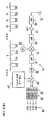
종래 기술의 기지국은 통상적으로 연속 주파수 스펙트럼을 수렴시키는 다중 캐리어를 이용할 것이 요구된다. 기지국에서 구현될 수 있는 종래 기술인 슈퍼헤테로다인(superheterodyne) 수신기(11)의 블록 다이어그램이 도 1에 도시된다. 운용자는 통상적으로 2개 이상의 채널(Ch1-Ch4)(캐리어)을 할당받고, 이들을 각 셀에서 사용할 것을 요구한다(주파수 재사용=1). 더 낮은 주파수 재사용 인자(frequency re-use factor)를 초래하는 일정한 제한들로 인하여 이러한 것이 가능하지 않은 경우, 운용자는 유한한 수의 채널을 가지며, 이들을 스펙트럼의 연속된 섹션들로 분할하여, 다수의 인접 채널들이 각 셀에서 사용될 수 있도록 한다. 이러한 경우, 수신기(11)는 모든 채널들(캐리어들)을 동시에 처리하도록 요구받는다. 이는 하드웨어 비용, 사이즈, 및 전력 소모를 최소화한다.Prior art base stations are typically required to use multiple carriers that converge on a continuous frequency spectrum. A block diagram of a prior
과거에는, 기지국 수신기의 높은 요구 조건들은 단지 슈퍼헤테로다인 아키텍쳐로만 충족될 수 있었다. 직접 변환 아키텍쳐는 RF 신호를 직접 기저대역으로 다운컨버팅하는데서 초래되는 다수의 내재된 문제점들을 가지고 있다. 이러한 문제점들은 기저대역 신호에 DC 오프셋을 생성하는 자기 혼합(self-mixing); 강한 간섭 신호를 기저대역으로 변환하는 짝수열 왜곡(even-order distortion); 모든 반도체 장치에 내재하고 주파수(f)에 반비례하며, 기저대역 신호를 마스크하는 1/f 잡음; 및 다른 사용자들을 간섭하는 LO 신호의 불요 전파(spurious emission)를 포함한다. 이득 제어 및 필터링 모두가 기저대역에서 행해져야 하기 때문에, 직접 변환 수신기는 또한 아날로그 기저대역 프로세싱 컴포넌트의 최신 성능을 강조한다. 이는 높은 동작 범위 및 광대역을 보유하는 비싼 증폭기를 요구한다.In the past, the high requirements of base station receivers could only be met with a superheterodyne architecture. Direct conversion architectures have a number of inherent problems that result from downconverting RF signals directly to baseband. These problems include self-mixing to generate a DC offset in the baseband signal; Even-order distortion, which transforms a strong interfering signal into baseband; 1 / f noise inherent in all semiconductor devices and inversely proportional to frequency f and masking the baseband signal; And spurious emission of the LO signal interfering with other users. Since both gain control and filtering must be done at baseband, the direct conversion receiver also highlights the latest performance of analog baseband processing components. This requires expensive amplifiers with high operating range and wide bandwidth.
종래의 다중 캐리어 전파는, 수신기를 위해 도 1에 도시된 바와 같이, 중간 주파수(IF) 및 직접 디지털 샘플링을 이용하는 슈퍼헤테로다인 무선 아키텍쳐에 기초하여, 다중 캐리어들을 기저대역과 상호 블록 변환할 수 있도록 한다. IF가 통상적으로 50MHz를 초과하는 범위에 있기 때문에, 직접 디지털 샘플링은 100MHz보다 큰 레이트를 샘플링할 수 있고 매우 낮은 클록 지터(clock jitter)를 요구하는 아날로그-디지털 컨버터(ADC) 및 디지털-아날로그 컨버터(DAC)와 같은 비싼 고속 또는 서브 샘플링 데이터 컨버터를 요구한다.Conventional multicarrier propagation is based on a superheterodyne wireless architecture using intermediate frequency (IF) and direct digital sampling, as shown in FIG. 1 for the receiver, to enable cross-carrier conversion of multiple carriers to baseband. do. Because the IF is typically in the range above 50 MHz, direct digital sampling can sample rates greater than 100 MHz and requires analog-to-digital converters (ADCs) and digital-to-analog converters (which require very low clock jitter). Expensive high-speed or sub-sampling data converters such as DAC).
직접 디지털 샘플링에 대한 또 다른 단점은 인접 채널에 간섭하는 것을 차단하기 위해 필요로 하는 IF 표면 탄성파(Surface Acoustic Wave; SAW)이다. 전파에 의해 지원되는 캐리어의 최대 수는 SAW 필터의 대역폭을 결정한다. 상이한 수의 캐리어들에 대한 지원은 추가적인 SAW 필터를 요구한다. 다른 대안으로서, 관심있는 전체 대역을 커버하는 하나의 IF 필터가 이용될 수 있으나, 추가적인 간섭을 처리하는데에는 ADC에서 추가적인 동작 범위가 필요하다.Another drawback to direct digital sampling is the IF Surface Acoustic Wave (SAW), which is required to block interference from adjacent channels. The maximum number of carriers supported by the propagation determines the bandwidth of the SAW filter. Support for different numbers of carriers requires additional SAW filters. Alternatively, one IF filter can be used that covers the entire band of interest, but additional operating range is required in the ADC to handle additional interference.
이는 수신되는 신호의 동작 범위로부터 이해할 수 있다. 업링크 채널이 모두 동일한 기지국의 제어하에 있을 때, 무선 주파수(RF) 캐리어는 유사한 전력 레벨에서 수신될 것이며, 이는 ADC에서 상대적으로 낮은 동작 범위를 요구한다. 그러나 IF 필터 대역폭이 전체 대역폭을 커버하는 경우, 다른 기지국에 속하는 업링크 채널은 ADC에 대한 입력부에 존재할 것이다. 이러한 채널은 매우 높은 레벨에 있을 수 있고, 따라서 ADC에서 더 높은 동작 범위를 요구한다.This can be understood from the operating range of the received signal. When the uplink channels are all under the control of the same base station, radio frequency (RF) carriers will be received at similar power levels, which requires a relatively low operating range in the ADC. However, if the IF filter bandwidth covers the entire bandwidth, an uplink channel belonging to another base station will be present at the input to the ADC. These channels can be at very high levels and therefore require higher operating range in the ADC.
다시 도 1을 참조하면, 수신기(11)는 디지털 다중 캐리어 무선 통신, 예를 들면, 코드 분할 다중 접속(CDMA) 통신을 위해 이용된다. 신호가 안테나(15)에서 수신될 때, 신호는 제1 대역 통과 필터(16) 및 선형 증폭기(17)를 통과한다. 제2 대역 통과 필터(18)는 증폭기(17)로부터 신호를 수신하고 혼합기(19)에 신호를 제공한다. 국부 발진기(20)는 혼합기(19)에 연결되고, 혼합기(19)는 그 신호를 RF에 서 IF로 옮기며, 이후 대역 통과 필터(21)에 의해 필터링된다.Referring again to FIG. 1, the
대역 통과 필터(21)는 디지털 다운 컨버터(23)에 디지털화된 출력을 제공하는 ADC(22)에 연결된다. 복합(complex) 수치 제어 발진기를 이용하여 디지털 다운 컨버터(23)를 제어함으로써 IF에서의 각 채널을 기저대역으로 옮길 수 있다. 디지털 다운 컨버터(23)는 직교 기저대역 신호(qudrature baseband signal)를 유한 임펄스 응답(FIR) 필터(25)의 뱅크에 제공하며, 이는 펄스 형성(pulse shaping) 및 간섭 차단(interference rejection)을 수행한다. FIR 필터(25)로부터의 출력은, 4개의 개별적인 채널(45)에서 출력을 제공하는 각 디지털 자동 이득 제어 회로(DAGC; 35)에 제공된다. 각 채널로부터의 디지털 데이터는, 데이터 변조 및 디코딩과 같은 또다른 처리를 위해 디지털 프로세서(도시되지 않음)에 전송된다. 4개의 채널이 예로서 도시되고 있지만, 당업자라면 임의의 수의 채널이 있을 수 있음을 알 수 있을 것이다.The
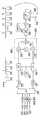
4개의 입력 채널(Ch1-Ch4)(65)을 이용하는 종래 기술의 송신기(51)를 도시하는 블록 다이어그램인 도 2에 도시된 바와 같이, 유사한 프로세스가 송신측 상에서 이용된다. 4개의 입력 채널(65)은, 개별 FIR 필터(85)에 그들의 출력을 차례로 제공하는 개별 전력 제어 회로(75)에 제공된다. FIR 필터(85)는 통상적으로 펄스 형성용으로 이용된다. FIR 필터(85)로부터의 출력은, 복합 수치 제어 발진기(96)에 연결되는 디지털 업 컨버터(95)에 직교로(in quadrature) 제공된다. 디지털 업 컨버터(95)의 출력은, 디지털-아날로그(DAC) 회로(97)에 제공되며, 그 아날로그 출력은 제1 대역 통과 필터(98)에 공급되어, 차례로 IF 혼합기(99)에 제공된다. IF 혼 합기(99)는 발진기(100)로부터 국부 발진기 신호를 수신하고 제2 대역 통과 필터(102)에 출력을 제공한다. 대역 통과 필터의 출력은 증폭기(103)에서 증폭되고, 대역 통과 필터(104)의 출력에서 필터링되어 제공됨으로써 안테나를 통해 송신된다.A similar process is used on the transmitting side, as shown in Figure 2, which is a block diagram showing a transmitter 51 of the prior art using four input channels (Ch1-Ch4) 65. Four
이러한 구성에 있어서(도 1 및 2), RF 컴포넌트들과 함께 다양한 변환들이 수행된다. 이러한 RF 컴포넌트들의 제조 비용은 상당하다. 그러므로, 실제 가능한 최대치까지 다중 RF 변환을 회피하는 회로를 제공하는 것이 이롭다. 부가적으로 수신기 및 송신기를 위한 직접 변환 설계가 요구된다.In this configuration (FIGS. 1 and 2), various transformations are performed with the RF components. The manufacturing cost of these RF components is significant. Therefore, it would be advantageous to provide a circuit that avoids multiple RF conversions to the maximum practically possible. In addition, a direct conversion design for the receiver and transmitter is required.
종래 기술의 직접 변환 수신기들의 문제점은 수신기의 출력부에서의 DC 오프셋 생성이다. DC 오프셋의 주요 원인은 혼합기의 2차 상호 변조(IP2) 및 국부 발진기 자기 혼합이다. DC 오프셋은 매우 클 수도 있으며, ADC의 포화 및 수신기에서의 다른 성능 문제점들을 이끈다.The problem with prior art direct conversion receivers is the DC offset generation at the output of the receiver. The main sources of DC offset are the mixer's second order intermodulation (IP2) and local oscillator magnetic mixing. The DC offset can be very large, leading to saturation of the ADC and other performance issues at the receiver.
직접 변환 문제점들에 대한 해법이 얼마간 알려져 왔으나, 이들은, 최근 기술 발전에 의해 단일 RF 통합 회로(RFIC) 상에서 가능한 통합 해법이 이루어질 때까지 실용적이지 못하거나 비용 효율적이지 않았다. 이러한 문제점들에 대한 해법은 짝수열 왜곡을 제거하는 밸런스된 (차동의) 구조, 낮은 1/f 및 탁월한 선형성을 나타내는 SiGe 반도체 기술, 및 자기 혼합 및 LO 불요 전파(spurious emission)를 제거하는 고조파 혼합(harmonic mixing)을 포함한다. 광대역 무선 기술로의 이동은 또한, 직접 변환 수신기의 전체 잡음층에 대한 1/f 잡음의 기여를 감소시켰다. 또한, 이제 고속, 고선형성 증폭기가 이용 가능하여 아날로그 기저대역 처리 요건을 충족시킬 수 있다.Although solutions to direct conversion problems have been known for some time, they have not been practical or cost effective until recent technological advances have made possible integrated solutions on a single RF integrated circuit (RFIC). The solution to these problems is a balanced (differential) structure that eliminates even-order distortion, SiGe semiconductor technology that exhibits low 1 / f and excellent linearity, and harmonic mixing that eliminates magnetic mixing and LO spurious emission. (harmonic mixing). The move to broadband wireless technology has also reduced the contribution of 1 / f noise to the overall noise floor of the direct conversion receiver. In addition, high-speed, high-linearity amplifiers are now available to meet analog baseband processing requirements.
그러나, 수신기의 출력부에서의 DC 오프셋의 생성에 있어서, 직접 변환 수신기와 함께 여전히 주요한 문제점이 있다. DC 오프셋의 주요한 원인은 혼합기의 2차 상호 변조 및 LO 자기 혼합이다. DC 오프셋은 매우 커서 ADC의 포화 및 수신기의 다른 성능 문제점들을 이끈다. 따라서, 종래 기술과 함께 진전이 있었지만, 이러한 종래 기술들은 여전히 최적의 성능을 내기에는 요원하다.However, there is still a major problem with the direct conversion receiver in generating the DC offset at the output of the receiver. The main sources of DC offset are the mixer's second order intermodulation and LO magnetic mixing. The DC offset is very large, leading to saturation of the ADC and other performance problems of the receiver. Thus, although progress has been made with the prior art, these prior arts are still far from optimal performance.
본 발명은 직접 변환, 다중 캐리어 프로세서를 포함하는, 수신기, 송신기 또는 송수신기와 같은 무선 통신 장치이다. 다중 캐리어 프로세서 주파수는, 쿼드러티브(quadrative) 변조기(송신기) 또는 복조기(수신기)를 이용하여, RF 채널과 기저대역간 서로를 옮긴다. 아날로그 신호는 DC에 근접하게 옮겨지므로, 종래의 조정 가능한 필터들이 대역폭 제어 장치를 통해 프로그램되어, 상이한 수의 채널(캐리어) 및 채널 대역폭을 지원할 수 있도록 한다.The present invention is a wireless communication device, such as a direct conversion, multi-carrier processor, such as a receiver, transmitter or transceiver. Multi-carrier processor frequencies use a quadrative modulator (transmitter) or demodulator (receiver) to transfer each other between RF channels and baseband. Since the analog signal is moved close to DC, conventional adjustable filters can be programmed through the bandwidth control device to support different numbers of channels (carriers) and channel bandwidths.
도 1은 직접 디지털 샘플링 다중 캐리어 수신기를 갖는 종래 기술의 슈퍼헤테로다인의 블록 다이어그램.1 is a block diagram of a prior art superheterodyne with a direct digital sampling multicarrier receiver.
도 2는 직접 디지털 송신기를 갖는 종래 기술의 슈퍼헤테로다인의 블록 다이어그램.2 is a block diagram of a prior art superheterodyne with a direct digital transmitter.
도 3은 본 발명에 따라 구성된 직접 변환 다중 캐리어 수신기의 블록 다이어그램.3 is a block diagram of a direct conversion multi-carrier receiver constructed in accordance with the present invention.
도 4는 본 발명에 따라 구성된 직접 변환 다중 캐리어 송신기의 블록 다이어 그램.4 is a block diagram of a direct conversion multi-carrier transmitter constructed in accordance with the present invention.
본 발명은 도면을 참조하여 설명될 것이며, 동일한 참조 번호는 동일한 엘리먼트를 나타낸다.The invention will be described with reference to the drawings, wherein like reference numerals refer to like elements.
본 발명은 직접 변환 송신기/수신기 및 기저대역 신호 처리를 이용하는 무선 통신 시스템에서 다중 RF 캐리어의 블록 처리를 가능하게 한다. 이러한 다중 캐리어 전파는, 별개 전파 내의 각 캐리어를 처리하기 보다는 단일 전파 내의 다중 캐리어를 동시에 처리함으로써 비용을 감소시킨다.The present invention enables block processing of multiple RF carriers in a wireless communication system using direct conversion transmitter / receiver and baseband signal processing. Such multicarrier propagation reduces costs by simultaneously processing multiple carriers within a single radio wave, rather than processing each carrier in separate radio waves.
도 3은 본 발명에 따라 구성된 통신 수신기(130)의 전형적인 실시예를 도시하는 블록 다이어그램이다. 수신기(130)는 다수의 통신 신호(Ch1, Ch2 ... Chn)를 수신하며, 이들 각각은 각 캐리어 주파수(F1, F2 ... Fn)를 통해 전송된다. 이러한 신호는 이후 총괄적으로 다중 캐리어 신호(S1)으로 언급될 것이다.3 is a block diagram illustrating an exemplary embodiment of a
수신기(130)는 안테나(131), 제1 대역 통과 필터(132), 무선 주파수 증폭기(133) 및 제2 대역 통과 필터(134)를 갖는다. 또한, 국부 발진기(143)에 연결되는 제1 및 제2 혼합기(141, 142), 제1 및 제2 저역 통과 필터(LPF)(145, 146), 대역폭 제어 회로(147) 및 제1 및 제2 기저대역 증폭기(151, 152)가 포함된다. 국부 발진기(143)와 결합된 제1 및 제2 혼합기(141, 142)는 복조기(144)를 포함한다.The
제1 자동 이득 제어(AGC) 회로(153)는 기저대역 증폭기(151, 152)에 연결되며, 기저대역 증폭기(151, 152)로부터의 출력은 ADC 회로(161, 162)에 제공된다. ADC(161, 162)로부터의 디지털화된 출력은 제2 AGC 회로(163)에 제공된다. 제2 AGC 회로(163)는 DAC(164)에 AGC 출력을 제공하며, 차례로 제1 AGC 회로(153)에 출력을 제공하고, 이로써 기저대역 증폭기(151, 152)의 이득을 제어한다.A first automatic gain control (AGC)
제2 AGC 회로(163)로부터의 출력은 디지털 다운 컨버터(171)에 제공되며, 이는 다수의 FIR 필터(181-195) 및 다수의 DAGC(191-195)에 차례로 개별적인 출력을 제공하여, 다수의 채널(Ch1-Chn)(198-202)에 출력을 제공한다. 디지털-아날로그 AGC 루프(163, 164, 153)를 이용함으로써, 출력부에서의 동작 범위를 감소시키고, 따라서 디지털 AGC 회로(191-194) 다운스트림의 필요한 동작 범위를 감소시킨다.The output from the
안테나(131)는 다중 캐리어 신호(S1)를 포착하고 그 신호(S1)를 대역 통과 필터(132)에 입력하여 대역 필터링을 제공함으로써, 대역 외의 간섭을 차단한다. 필터링 후, 그 신호는 수신기(130)의 잡음층을 설정하는 저역 잡음 증폭기(LNA)(133)에 입력된다. LNA(133)의 출력은 대역 통과 필터(BPF)(134)를 통해 필터링되어 LNA(133)에 의해 생성된 임의의 상호 변조 왜곡을 필터링할 수 있다.The
LNA(133)의 출력은 복조기(144)에 전송되며, 이는 혼합기(141 및 143) 및 안정 국부 발진기(LO)(143)로 구성된다. LO(143)는 2개의 출력을 가지며, 캐리어에 대해 상대적으로 하나는 동위상(in-phase)(I)이고 하나는 직교(in quadrature)(Q)이다. LO(143)의 주파수는 입력 채널(Ch1-Chn)의 중심 주파수인 (F1 - Fn)/2이다; 여기에서 F1은 제1 채널 Ch1의 캐리어 주파수이고, Fn은 n번째 채널 Chn의 캐리어 주파수이다. 복조기(144)는 원하는 신호를 RF에서 기적대역으로 옮겨서, DC 주위의 신호를 집중시킨다.The output of
I 및 Q 신호는 LPF(145 및 146)에 전송되어 간섭 차단을 제공함으로써, 다운스트림 기저대역 프로세싱 엘리먼트들(151-194)의 동작 범위를 최소화할 수 있다. 아날로그 신호는 DC 근처로 옮겨지기 때문에, 종래의 조정 가능한 필터(145 및 146)는 대역폭 제어(147)를 통해 프로그램되어, 상이한 수의 채널 및 재널 대역폭을 지원할 수 있다.I and Q signals may be sent to
ADC(161, 162)는 복조기(144)로부터의 I/Q 신호를 디지털화하는 한쌍의 종래의 저렴한 ADC이다. 개별 채널(Ch1-Chn)은 DDC(171)에 의해 기저대역으로 다운컨버팅된다.
채널 필터링 및 펄스 형성은 FIR 필터(181-185)에 의해 각 채널(Ch1-Chn)에 적용된다.Channel filtering and pulse shaping is applied to each channel Ch1 -Chn by FIR filters 181-185.
AGC 과정은 두 단계로 수행된다. 제1 단계는 제1 및 2 AGC 회로(151, 163)에서 수행되어 기저대역 증폭기(151, 152)의 이득을 조정함으로써 ADC(161, 162)의 동작 범위 내에서 그 신호를 유지한다. AGC 과정의 제2 단계는 DAGC 블록(191-195)에서 디지털적으로 수행되고, I/Q 신호의 대역폭을 각 채널(198-202)에 대해 필요한 최소치까지 감소시키기 위해 이용된다.The AGC process is carried out in two stages. The first step is performed in the first and
도 3에 도시된 바와 같이, 수신기(130)는 다중 캐리어 직접 변환 수신기로서 동작한다. 이것에 의해 다중 RF 채널을 포함하는 주파수 블록은 직접적으로 주파수 블록으로서 기저대역으로 다운컨버팅된다.As shown in FIG. 3,
도 4는 본 발명에 따라 구성된 직접 변환 통신 송신기(230)의 전형적인 실시예를 도시하는 블록 다이어그램이다. 개별적인 채널(Ch1-Chn)(231-234)은 우선 FIR 필터(241-244)를 통해 전송되고 디지털 업 컨버터 DUC(247)에 의해 디지털적으로 업컨버팅된다. 이는 디지털 기저대역 신호를 제공하며, 이를 이용하여 한쌍의 저렴한 DAC(251, 252)를 구동할 수 있다. DUC(247)는 중심 주파수를 0에서 그 대역폭의 절반의 +/- 위치로 이동시킴으로써 입력 신호를 I/Q 신호 컴포넌트로 변환한다.4 is a block diagram illustrating an exemplary embodiment of a direct
DUC(247)의 출력은 직교로(in quadrature) 분리되는 2개의 디지털 출력을 포함한다. 이러한 I/Q 출력은 DAC(251 및 252)에 입력되어, 디지털 신호를 아날로그로 변환한다. DAC(251, 252)로부터의 아날로그 출력은 LPF(253, 254)에 제공되며, 이러한 LPF의 대역폭은 대역폭 제어 회로(255)에 의해 제어된다. LPF(253, 254)는 아날로그 신호를 필터링하고, 2개의 혼합기(261, 262), LO(263) 및 가산기(264)를 포함하는 변조기(260)에 그들의 각 필터링된 출력을 제공한다. 혼합기(261, 262)는 LO(263)에 의해 제어되고, 혼합된 출력을 가산기(264)에 제공한다. 변조기(260)는 대역 통과 필터(265), 제1 RF 증폭기(266)에 차례로 출력을 제공한다. RF 증폭기(266)는 이득 제어 회로(267)에 의해 제어되고, 대역 통과 필터(268), 및 안테나(270)를 통한 송신용 신호를 증폭하는 RF 전력 증폭기(269)에 출력을 제공한다.The output of the
도 3 및 4에서 명확히 보여지는 바와 같이, 본 발명에 따른 직접 변환 다중 캐리어 프로세서는 IF 단계를 제거함으로써 슈퍼헤테로다인 전파의 단점을 회피한다. 이로써 전파에 있어서 비용을 절감시키며, 데이터 컨버터가 더 낮은 클록 레이트로 기저대역에서 동작할 수 있도록 하며, 이 또한 비용을 절감시킨다. 조정 가능한 대역폭 필터는 기저대역에서 즉시 실현 가능하고, 이로써 가변 캐리어 공간 및 캐리어 수에 대한 유연한 지원이 전파에서 처리될 수 있도록 한다. 이는 또한 단지 원하는 캐리어만 ADC에서 존재하기 때문에 ADC에서 요구되는 동작 범위를 감소시켜, 다시 비용을 절감시킬 수 있다.As clearly shown in Figures 3 and 4, the direct conversion multi-carrier processor according to the present invention avoids the disadvantages of superheterodyne propagation by eliminating the IF step. This reduces the cost of propagation and allows the data converter to operate at baseband at a lower clock rate, which also saves money. Adjustable bandwidth filters are immediately feasible at baseband, allowing flexible support for variable carrier space and number of carriers to be handled in the airwaves. It also reduces the operating range required by the ADC since only the desired carriers are present in the ADC, which in turn can reduce costs.
본 발명은 무선 로컬 루프, 무선 LAN 애플리케이션, 및 WCDMA(UTRATDD 및 UTRAFDD 양자 모두), TDSCDMA, CDMA2000, 3xRT, 및 OFDMA 시스템과 같은 셀룰러 시스템을 포함하는 무선 통신 시스템에 적용 가능하다.The present invention is applicable to wireless communication systems including wireless local loops, wireless LAN applications, and cellular systems such as WCDMA (both UTRATDD and UTRAFDD), TDSCDMA, CDMA2000, 3xRT, and OFDMA systems.
본 발명이 바람직한 실시예에 대하여 설명되었지만, 당업자라면 이하 청구범위에서 아웃라인된 벌명의 범위 내에서의 다양한 변화들은 자명할 것이다.Although the present invention has been described with respect to the preferred embodiments, various changes within the scope of the claims outlined in the claims below will be apparent.
Claims (12)
Translated fromKoreanApplications Claiming Priority (3)
| Application Number | Priority Date | Filing Date | Title |
|---|---|---|---|
| US38720702P | 2002-06-07 | 2002-06-07 | |
| US60/387,207 | 2002-06-07 | ||
| PCT/US2003/017851WO2003105390A2 (en) | 2002-06-07 | 2003-06-05 | System and method for a direct conversion multi-carrier processor |
Related Child Applications (1)
| Application Number | Title | Priority Date | Filing Date |
|---|---|---|---|
| KR1020057017487ADivisionKR20050096208A (en) | 2002-06-07 | 2003-06-05 | System and method for a direct conversion multi-carrier processor |
Publications (2)
| Publication Number | Publication Date |
|---|---|
| KR20050014850A KR20050014850A (en) | 2005-02-07 |
| KR100671364B1true KR100671364B1 (en) | 2007-01-22 |
Family
ID=29736279
Family Applications (3)
| Application Number | Title | Priority Date | Filing Date |
|---|---|---|---|
| KR1020047019912AExpired - Fee RelatedKR100671364B1 (en) | 2002-06-07 | 2003-06-05 | Method and system for direct conversion multicarrier processor |
| KR1020057017487AWithdrawnKR20050096208A (en) | 2002-06-07 | 2003-06-05 | System and method for a direct conversion multi-carrier processor |
| KR1020087013473AWithdrawnKR20080059339A (en) | 2002-06-07 | 2003-06-05 | Method and system for direct conversion multicarrier processor |
Family Applications After (2)
| Application Number | Title | Priority Date | Filing Date |
|---|---|---|---|
| KR1020057017487AWithdrawnKR20050096208A (en) | 2002-06-07 | 2003-06-05 | System and method for a direct conversion multi-carrier processor |
| KR1020087013473AWithdrawnKR20080059339A (en) | 2002-06-07 | 2003-06-05 | Method and system for direct conversion multicarrier processor |
Country Status (12)
| Country | Link |
|---|---|
| US (2) | US7162218B2 (en) |
| EP (2) | EP1522151B1 (en) |
| JP (1) | JP4152944B2 (en) |
| KR (3) | KR100671364B1 (en) |
| CN (2) | CN100426690C (en) |
| AR (1) | AR040160A1 (en) |
| AU (1) | AU2003238923A1 (en) |
| CA (1) | CA2488740A1 (en) |
| MX (1) | MXPA04012249A (en) |
| NO (1) | NO20045559L (en) |
| TW (3) | TWI237450B (en) |
| WO (1) | WO2003105390A2 (en) |
Families Citing this family (39)
| Publication number | Priority date | Publication date | Assignee | Title |
|---|---|---|---|---|
| DE60111056T2 (en)* | 2001-10-26 | 2006-05-04 | Stmicroelectronics N.V. | Direct match receiver for a non-constant envelope communication system |
| DE10253671B3 (en)* | 2002-11-18 | 2004-08-19 | Infineon Technologies Ag | Suppression of adjacent channel interference through adaptive channel filtering in mobile radio receivers |
| DE60239349D1 (en)* | 2002-12-18 | 2011-04-14 | Texas Instruments Inc | Message receiver with automatic gain control |
| US7995684B2 (en)* | 2003-02-01 | 2011-08-09 | Qualcomm, Incorporated | Method and apparatus for automatic gain control of a multi-carrier signal in a communication receiver |
| US20050053127A1 (en)* | 2003-07-09 | 2005-03-10 | Muh-Tian Shiue | Equalizing device and method |
| US7869528B2 (en)* | 2003-10-31 | 2011-01-11 | Northrop Grumman Systems Corporation | Multi-carrier transceiver assembly |
| US7664520B2 (en)* | 2004-06-24 | 2010-02-16 | Nokia Corporation | Low current direct conversion transmitter architecture |
| JP4708076B2 (en)* | 2005-04-14 | 2011-06-22 | 三星電子株式会社 | Down converter and up converter |
| US8000302B2 (en) | 2005-06-23 | 2011-08-16 | Qualcomm Incorporated | Adaptive multi-channel modem |
| US7477879B1 (en)* | 2005-06-30 | 2009-01-13 | Silicon Laboratories, Inc. | Transceiver system with common receiver and transmitter oscillator |
| US8693525B2 (en) | 2006-07-14 | 2014-04-08 | Qualcomm Incorporated | Multi-carrier transmitter for wireless communication |
| US8295371B2 (en) | 2006-07-14 | 2012-10-23 | Qualcomm Incorporated | Multi-carrier receiver for wireless communication |
| KR100789784B1 (en) | 2006-10-11 | 2007-12-28 | 한국전자통신연구원 | Receiving device supporting scalable bandwidth and method |
| WO2008044868A1 (en)* | 2006-10-11 | 2008-04-17 | Electronics And Telecommunications Research Institute | Receiver and receiving method for scalable bandwidth |
| US7826815B2 (en)* | 2007-07-13 | 2010-11-02 | Fairchild Semiconductor Corporation | Dynamic selection of oscillation signal frequency for power converter |
| US7945217B2 (en)* | 2007-11-13 | 2011-05-17 | Provigent Ltd. | Multi-mode baseband-IF converter |
| FI20075958A0 (en) | 2007-12-21 | 2007-12-21 | Nokia Corp | Processing of broadcast signals in a radio transmitter |
| US7991368B2 (en)* | 2007-12-27 | 2011-08-02 | Provigent Ltd | Integrated RF-IF converter |
| GB2458908B (en)* | 2008-04-01 | 2010-02-24 | Michael Frank Castle | Low power signal processor |
| EP2313982A1 (en)* | 2008-07-28 | 2011-04-27 | Freescale Semiconductor, Inc. | Semiconductor device wireless communication unit and method for receiving a signal |
| US20100119009A1 (en)* | 2008-11-11 | 2010-05-13 | Flexiradio, Llc | Programmable wide band digital receiver/transmitter |
| US8514982B2 (en)* | 2008-12-12 | 2013-08-20 | CSR Technology, Inc | Systems and methods for digitizing multiple channels in a receiver |
| KR101489964B1 (en)* | 2009-09-01 | 2015-02-06 | 한국전자통신연구원 | Receiving apparatus and receiving method |
| EP2290828B1 (en) | 2009-09-01 | 2016-11-09 | Electronics and Telecommunications Research Institute | Receiving apparatus and receiving method |
| US20110053536A1 (en)* | 2009-09-03 | 2011-03-03 | Provigent Ltd | Receiver with re-demodulation |
| US8547207B2 (en)* | 2010-03-11 | 2013-10-01 | Checkpoint System, Inc. | RFID converter module |
| DE102010027566A1 (en)* | 2010-05-18 | 2011-11-24 | Rohde & Schwarz Gmbh & Co. Kg | Signal generator with digital intermediate frequency and digital fine tuning |
| US8903330B2 (en) | 2010-12-13 | 2014-12-02 | Huawei Technologies Co., Ltd. | Communication signal transmission method, device and system |
| CN102104392B (en) | 2010-12-15 | 2013-10-09 | 华为技术有限公司 | Multi-band multi-channel transceiver equipment and method, base station system |
| US8406709B2 (en) | 2011-02-27 | 2013-03-26 | Provigent Ltd. | Carrier recovery in re-modulation communication systems |
| JP6096198B2 (en)* | 2011-09-15 | 2017-03-15 | インテル コーポレイション | Predistortion linearization communication system, predistortion linearization method, computer program, and storage device |
| EP2573997A1 (en)* | 2011-09-26 | 2013-03-27 | Thomson Licensing | Method for controlling bandwidth and corresponding device |
| GB2504973B (en)* | 2012-08-15 | 2014-11-19 | Broadcom Corp | Receiver circuit |
| KR101367236B1 (en)* | 2013-06-24 | 2014-02-26 | 주식회사 삼정솔루션 | Apparatus for protecting signal |
| CN105048966A (en)* | 2015-06-12 | 2015-11-11 | 中国电子科技集团公司第四十一研究所 | Multi-phase digital down conversion method for GHz high-speed sampling signal |
| US10191454B2 (en)* | 2016-06-13 | 2019-01-29 | William Marsh Rice University | Methods and related systems of ultra-short pulse detection |
| WO2019148296A1 (en) | 2018-02-02 | 2019-08-08 | Ats Automation Tooling Systems Inc. | Linear motor conveyor system for clean/aseptic environments |
| CN116707734A (en) | 2019-04-30 | 2023-09-05 | 华为技术有限公司 | Method and related device for transmitting sounding reference signal |
| KR102426630B1 (en)* | 2022-04-12 | 2022-07-28 | 한화시스템(주) | RF signal processing device and method for low orbit satellite |
Family Cites Families (35)
| Publication number | Priority date | Publication date | Assignee | Title |
|---|---|---|---|---|
| US4654800A (en)* | 1984-02-20 | 1987-03-31 | Kabushikikaisha Nippon Coinco | Control and monitoring apparatus for vending machines |
| US5095536A (en)* | 1990-03-23 | 1992-03-10 | Rockwell International Corporation | Direct conversion receiver with tri-phase architecture |
| WO1993026094A1 (en)* | 1992-06-08 | 1993-12-23 | Motorola, Inc. | Receiver automatic gain control |
| FR2707063B1 (en)* | 1993-06-25 | 1995-09-22 | Alcatel Mobile Comm France | |
| US5519732A (en)* | 1994-05-02 | 1996-05-21 | Harris Corporation | Digital baseband to IF conversion in cellular base stations |
| JPH0832464A (en)* | 1994-07-15 | 1996-02-02 | Uniden Corp | Carrier leak correction method in transmitter |
| US5715314A (en)* | 1994-10-24 | 1998-02-03 | Open Market, Inc. | Network sales system |
| US5758257A (en)* | 1994-11-29 | 1998-05-26 | Herz; Frederick | System and method for scheduling broadcast of and access to video programs and other data using customer profiles |
| US5579341A (en)* | 1994-12-29 | 1996-11-26 | Motorola, Inc. | Multi-channel digital transceiver and method |
| US7937312B1 (en)* | 1995-04-26 | 2011-05-03 | Ebay Inc. | Facilitating electronic commerce transactions through binding offers |
| US6009130A (en)* | 1995-12-28 | 1999-12-28 | Motorola, Inc. | Multiple access digital transmitter and receiver |
| FI112133B (en)* | 1996-03-29 | 2003-10-31 | Nokia Corp | Method of forming the frequencies of a direct conversion transmitter / receiver operating in two different frequency ranges and a direct conversion transmitter / receiver of a radio communication system operating in two different frequency ranges and using the foregoing in a mobile telephone |
| KR0164419B1 (en)* | 1996-04-19 | 1999-02-01 | 김광호 | Automatic Gain Control Circuit of Wireless Receiver |
| US5898912A (en)* | 1996-07-01 | 1999-04-27 | Motorola, Inc. | Direct current (DC) offset compensation method and apparatus |
| US6005894A (en) | 1997-04-04 | 1999-12-21 | Kumar; Derek D. | AM-compatible digital broadcasting method and system |
| US6029052A (en)* | 1997-07-01 | 2000-02-22 | Telefonaktiebolaget Lm Ericsson | Multiple-mode direct conversion receiver |
| IT1294284B1 (en)* | 1997-07-29 | 1999-03-24 | Italtel Spa | WIDE BAND RADIO TRANSMITTER FOR A SIGNAL CONSTITUTED BY A PLURALITY OF EQUIPPED DIGITALLY MODULATED CARRIERS |
| IT1297278B1 (en) | 1997-09-15 | 1999-08-09 | Italtel Spa | WIDE BAND DIGITAL RADIO RECEIVER FOR MULTIPORTANT SIGNAL |
| AUPP261898A0 (en)* | 1998-03-27 | 1998-04-23 | Victoria University Of Technology | Dc offset and im2 removal in direct conversion receivers |
| CN1120602C (en)* | 1998-04-14 | 2003-09-03 | 弗兰霍菲尔运输应用研究公司 | Method and device for fine frequency synchronization in multi-carrier demodulation system |
| JP3319422B2 (en)* | 1998-05-08 | 2002-09-03 | 日本電気株式会社 | Multi-carrier transmission system and multi-carrier transmission method |
| US7106689B1 (en)* | 1999-03-02 | 2006-09-12 | Matsushita Electric Industrial Co., Ltd. | OFDM transmission/reception apparatus |
| US7149726B1 (en)* | 1999-06-01 | 2006-12-12 | Stamps.Com | Online value bearing item printing |
| JP3551841B2 (en)* | 1999-06-09 | 2004-08-11 | 日本電気株式会社 | Receiver and gain control method thereof |
| US6480528B1 (en)* | 1999-06-11 | 2002-11-12 | Qualcomm Incorporated | Automatic gain control for improved decoding of multi-carrier signal |
| US6631170B1 (en)* | 1999-12-03 | 2003-10-07 | Nokia Corporation | Radio frequency receiver |
| US7213005B2 (en)* | 1999-12-09 | 2007-05-01 | International Business Machines Corporation | Digital content distribution using web broadcasting services |
| JP4652546B2 (en)* | 2000-09-21 | 2011-03-16 | 三星電子株式会社 | Receiving machine |
| US6560448B1 (en)* | 2000-10-02 | 2003-05-06 | Intersil Americas Inc. | DC compensation system for a wireless communication device configured in a zero intermediate frequency architecture |
| US7260141B2 (en)* | 2001-02-28 | 2007-08-21 | Itt Manufacturing Enterprises, Inc. | Integrated beamformer/modem architecture |
| US20020127982A1 (en)* | 2001-03-07 | 2002-09-12 | Nokia Mobile Phones Ltd | Mobile station receiver operable for both single and multi-carrier reception |
| KR100446540B1 (en)* | 2001-04-16 | 2004-09-01 | 삼성전자주식회사 | Transmitter for a data communication |
| US7243153B2 (en)* | 2001-06-26 | 2007-07-10 | Eastman Kodak Company | System and method for managing images over a communication network |
| US20030078011A1 (en)* | 2001-10-18 | 2003-04-24 | Integrated Programmable Communications, Inc. | Method for integrating a plurality of radio systems in a unified transceiver structure and the device of the same |
| US6819910B2 (en)* | 2002-03-08 | 2004-11-16 | Broadcom Corp. | Radio employing a self calibrating transmitter with reuse of receiver circuitry |
- 2003
- 2003-06-05TWTW092115312Apatent/TWI237450B/ennot_activeIP Right Cessation
- 2003-06-05KRKR1020047019912Apatent/KR100671364B1/ennot_activeExpired - Fee Related
- 2003-06-05TWTW095119778Apatent/TW200715777A/enunknown
- 2003-06-05JPJP2004512332Apatent/JP4152944B2/ennot_activeExpired - Fee Related
- 2003-06-05CNCNB038131463Apatent/CN100426690C/ennot_activeExpired - Fee Related
- 2003-06-05AUAU2003238923Apatent/AU2003238923A1/ennot_activeAbandoned
- 2003-06-05KRKR1020057017487Apatent/KR20050096208A/ennot_activeWithdrawn
- 2003-06-05EPEP03734443.9Apatent/EP1522151B1/ennot_activeExpired - Lifetime
- 2003-06-05KRKR1020087013473Apatent/KR20080059339A/ennot_activeWithdrawn
- 2003-06-05CNCNA2008101660484Apatent/CN101425811A/enactivePending
- 2003-06-05EPEP16154053.9Apatent/EP3032755A1/ennot_activeWithdrawn
- 2003-06-05CACA002488740Apatent/CA2488740A1/ennot_activeAbandoned
- 2003-06-05MXMXPA04012249Apatent/MXPA04012249A/enactiveIP Right Grant
- 2003-06-05TWTW093104385Apatent/TWI320637B/ennot_activeIP Right Cessation
- 2003-06-05WOPCT/US2003/017851patent/WO2003105390A2/enactiveApplication Filing
- 2003-06-06ARARP030102016Apatent/AR040160A1/enactiveIP Right Grant
- 2003-06-06USUS10/456,300patent/US7162218B2/ennot_activeExpired - Lifetime
- 2004
- 2004-12-20NONO20045559Apatent/NO20045559L/ennot_activeApplication Discontinuation
- 2006
- 2006-11-22USUS11/562,802patent/US20070085718A1/ennot_activeAbandoned
Also Published As
| Publication number | Publication date |
|---|---|
| EP1522151A4 (en) | 2006-05-17 |
| US20070085718A1 (en) | 2007-04-19 |
| WO2003105390A3 (en) | 2004-04-01 |
| TW200715777A (en) | 2007-04-16 |
| TWI320637B (en) | 2010-02-11 |
| KR20050014850A (en) | 2005-02-07 |
| CN100426690C (en) | 2008-10-15 |
| CN1706109A (en) | 2005-12-07 |
| AU2003238923A8 (en) | 2003-12-22 |
| TW200400700A (en) | 2004-01-01 |
| TWI237450B (en) | 2005-08-01 |
| MXPA04012249A (en) | 2005-02-25 |
| KR20080059339A (en) | 2008-06-26 |
| AU2003238923A1 (en) | 2003-12-22 |
| KR20050096208A (en) | 2005-10-05 |
| US20040072547A1 (en) | 2004-04-15 |
| EP1522151B1 (en) | 2016-03-23 |
| WO2003105390A2 (en) | 2003-12-18 |
| JP2005529544A (en) | 2005-09-29 |
| EP1522151A2 (en) | 2005-04-13 |
| NO20045559L (en) | 2004-12-20 |
| AR040160A1 (en) | 2005-03-16 |
| JP4152944B2 (en) | 2008-09-17 |
| CA2488740A1 (en) | 2003-12-18 |
| US7162218B2 (en) | 2007-01-09 |
| TW200501594A (en) | 2005-01-01 |
| CN101425811A (en) | 2009-05-06 |
| EP3032755A1 (en) | 2016-06-15 |
Similar Documents
| Publication | Publication Date | Title |
|---|---|---|
| KR100671364B1 (en) | Method and system for direct conversion multicarrier processor | |
| JP5608939B2 (en) | Receiver, transmitter, feedback device, transceiver, and signal processing method | |
| US5557642A (en) | Direct conversion receiver for multiple protocols | |
| EP1168646B1 (en) | A channelizer for a multi-carrier receiver | |
| US7924802B2 (en) | Wireless communication systems and methods | |
| WO2002095962A2 (en) | Quadrature envelope-sampling of intermediate frequency signal in receiver | |
| US8620226B2 (en) | Enhanced wideband transceiver | |
| KR20010062641A (en) | Dual digital low IF complex receiver | |
| EP1168638B1 (en) | A multi-carrier receiver for a wireless telecommunication system | |
| JP2002043946A (en) | Continuous time delta-sigma modulator | |
| CN112910476A (en) | Anti-blocking interference broadband receiving equipment | |
| US6118810A (en) | Multi-channel base station/terminal design covering complete system frequency range | |
| JP2002290367A (en) | Band division demodulation method and OFDM receiver | |
| EP1168641B1 (en) | A multi-carrier receiver including an analog-to-digital converter for a wireless telecommunication system | |
| JP2002335177A (en) | Wireless device | |
| HK1081339A2 (en) | System and method for a direct conversion multi-carrier processor | |
| KR100715205B1 (en) | Multiband Digital Transceiver and Method for Wireless Communication System | |
| EP1168640B1 (en) | Architecture for multi-carrier receiver | |
| Efstathiou | Base station transceiver trends for 3G and beyond wireless systems | |
| Efstathiou | SoftCell/sup TM: a multi-carrier chip-set for software definable radio base-stations | |
| Prithviraj et al. | Front End Architecture Design of Software Defined Radio Interoperable BTS between GSM and IS-95 | |
| JOSHI | Software Defined Radio |
Legal Events
| Date | Code | Title | Description |
|---|---|---|---|
| A201 | Request for examination | ||
| PA0105 | International application | St.27 status event code:A-0-1-A10-A15-nap-PA0105 | |
| PA0201 | Request for examination | St.27 status event code:A-1-2-D10-D11-exm-PA0201 | |
| P11-X000 | Amendment of application requested | St.27 status event code:A-2-2-P10-P11-nap-X000 | |
| P13-X000 | Application amended | St.27 status event code:A-2-2-P10-P13-nap-X000 | |
| P11-X000 | Amendment of application requested | St.27 status event code:A-2-2-P10-P11-nap-X000 | |
| P13-X000 | Application amended | St.27 status event code:A-2-2-P10-P13-nap-X000 | |
| R15-X000 | Change to inventor requested | St.27 status event code:A-3-3-R10-R15-oth-X000 | |
| R16-X000 | Change to inventor recorded | St.27 status event code:A-3-3-R10-R16-oth-X000 | |
| PG1501 | Laying open of application | St.27 status event code:A-1-1-Q10-Q12-nap-PG1501 | |
| R17-X000 | Change to representative recorded | St.27 status event code:A-3-3-R10-R17-oth-X000 | |
| A107 | Divisional application of patent | ||
| PA0104 | Divisional application for international application | St.27 status event code:A-0-1-A10-A18-div-PA0104 St.27 status event code:A-0-1-A10-A16-div-PA0104 | |
| R18-X000 | Changes to party contact information recorded | St.27 status event code:A-3-3-R10-R18-oth-X000 | |
| E902 | Notification of reason for refusal | ||
| PE0902 | Notice of grounds for rejection | St.27 status event code:A-1-2-D10-D21-exm-PE0902 | |
| P11-X000 | Amendment of application requested | St.27 status event code:A-2-2-P10-P11-nap-X000 | |
| P13-X000 | Application amended | St.27 status event code:A-2-2-P10-P13-nap-X000 | |
| E701 | Decision to grant or registration of patent right | ||
| PE0701 | Decision of registration | St.27 status event code:A-1-2-D10-D22-exm-PE0701 | |
| GRNT | Written decision to grant | ||
| PR0701 | Registration of establishment | St.27 status event code:A-2-4-F10-F11-exm-PR0701 | |
| PR1002 | Payment of registration fee | St.27 status event code:A-2-2-U10-U12-oth-PR1002 Fee payment year number:1 | |
| PG1601 | Publication of registration | St.27 status event code:A-4-4-Q10-Q13-nap-PG1601 | |
| PR1001 | Payment of annual fee | St.27 status event code:A-4-4-U10-U11-oth-PR1001 Fee payment year number:4 | |
| PR1001 | Payment of annual fee | St.27 status event code:A-4-4-U10-U11-oth-PR1001 Fee payment year number:5 | |
| PR1001 | Payment of annual fee | St.27 status event code:A-4-4-U10-U11-oth-PR1001 Fee payment year number:6 | |
| FPAY | Annual fee payment | Payment date:20121220 Year of fee payment:7 | |
| PR1001 | Payment of annual fee | St.27 status event code:A-4-4-U10-U11-oth-PR1001 Fee payment year number:7 | |
| R18-X000 | Changes to party contact information recorded | St.27 status event code:A-5-5-R10-R18-oth-X000 | |
| FPAY | Annual fee payment | Payment date:20131219 Year of fee payment:8 | |
| PR1001 | Payment of annual fee | St.27 status event code:A-4-4-U10-U11-oth-PR1001 Fee payment year number:8 | |
| PR1001 | Payment of annual fee | St.27 status event code:A-4-4-U10-U11-oth-PR1001 Fee payment year number:9 | |
| R17-X000 | Change to representative recorded | St.27 status event code:A-5-5-R10-R17-oth-X000 | |
| FPAY | Annual fee payment | Payment date:20160104 Year of fee payment:10 | |
| PR1001 | Payment of annual fee | St.27 status event code:A-4-4-U10-U11-oth-PR1001 Fee payment year number:10 | |
| FPAY | Annual fee payment | Payment date:20170102 Year of fee payment:11 | |
| PR1001 | Payment of annual fee | St.27 status event code:A-4-4-U10-U11-oth-PR1001 Fee payment year number:11 | |
| LAPS | Lapse due to unpaid annual fee | ||
| PC1903 | Unpaid annual fee | St.27 status event code:A-4-4-U10-U13-oth-PC1903 Not in force date:20180113 Payment event data comment text:Termination Category : DEFAULT_OF_REGISTRATION_FEE | |
| PC1903 | Unpaid annual fee | St.27 status event code:N-4-6-H10-H13-oth-PC1903 Ip right cessation event data comment text:Termination Category : DEFAULT_OF_REGISTRATION_FEE Not in force date:20180113 |