KR100669740B1 - Flat panel display - Google Patents
Flat panel displayDownload PDFInfo
- Publication number
- KR100669740B1 KR100669740B1KR1020040086129AKR20040086129AKR100669740B1KR 100669740 B1KR100669740 B1KR 100669740B1KR 1020040086129 AKR1020040086129 AKR 1020040086129AKR 20040086129 AKR20040086129 AKR 20040086129AKR 100669740 B1KR100669740 B1KR 100669740B1
- Authority
- KR
- South Korea
- Prior art keywords
- electrode
- conductive pattern
- pixel electrode
- pixel
- substrate
- Prior art date
- Legal status (The legal status is an assumption and is not a legal conclusion. Google has not performed a legal analysis and makes no representation as to the accuracy of the status listed.)
- Expired - Lifetime
Links
Images


Classifications
- H—ELECTRICITY
- H10—SEMICONDUCTOR DEVICES; ELECTRIC SOLID-STATE DEVICES NOT OTHERWISE PROVIDED FOR
- H10K—ORGANIC ELECTRIC SOLID-STATE DEVICES
- H10K59/00—Integrated devices, or assemblies of multiple devices, comprising at least one organic light-emitting element covered by group H10K50/00
- H10K59/10—OLED displays
- H10K59/12—Active-matrix OLED [AMOLED] displays
- G—PHYSICS
- G09—EDUCATION; CRYPTOGRAPHY; DISPLAY; ADVERTISING; SEALS
- G09G—ARRANGEMENTS OR CIRCUITS FOR CONTROL OF INDICATING DEVICES USING STATIC MEANS TO PRESENT VARIABLE INFORMATION
- G09G3/00—Control arrangements or circuits, of interest only in connection with visual indicators other than cathode-ray tubes
- G09G3/20—Control arrangements or circuits, of interest only in connection with visual indicators other than cathode-ray tubes for presentation of an assembly of a number of characters, e.g. a page, by composing the assembly by combination of individual elements arranged in a matrix no fixed position being assigned to or needed to be assigned to the individual characters or partial characters
- G09G3/22—Control arrangements or circuits, of interest only in connection with visual indicators other than cathode-ray tubes for presentation of an assembly of a number of characters, e.g. a page, by composing the assembly by combination of individual elements arranged in a matrix no fixed position being assigned to or needed to be assigned to the individual characters or partial characters using controlled light sources
- G09G3/30—Control arrangements or circuits, of interest only in connection with visual indicators other than cathode-ray tubes for presentation of an assembly of a number of characters, e.g. a page, by composing the assembly by combination of individual elements arranged in a matrix no fixed position being assigned to or needed to be assigned to the individual characters or partial characters using controlled light sources using electroluminescent panels
- G09G3/32—Control arrangements or circuits, of interest only in connection with visual indicators other than cathode-ray tubes for presentation of an assembly of a number of characters, e.g. a page, by composing the assembly by combination of individual elements arranged in a matrix no fixed position being assigned to or needed to be assigned to the individual characters or partial characters using controlled light sources using electroluminescent panels semiconductive, e.g. using light-emitting diodes [LED]
- G09G3/3208—Control arrangements or circuits, of interest only in connection with visual indicators other than cathode-ray tubes for presentation of an assembly of a number of characters, e.g. a page, by composing the assembly by combination of individual elements arranged in a matrix no fixed position being assigned to or needed to be assigned to the individual characters or partial characters using controlled light sources using electroluminescent panels semiconductive, e.g. using light-emitting diodes [LED] organic, e.g. using organic light-emitting diodes [OLED]
- G09G3/3225—Control arrangements or circuits, of interest only in connection with visual indicators other than cathode-ray tubes for presentation of an assembly of a number of characters, e.g. a page, by composing the assembly by combination of individual elements arranged in a matrix no fixed position being assigned to or needed to be assigned to the individual characters or partial characters using controlled light sources using electroluminescent panels semiconductive, e.g. using light-emitting diodes [LED] organic, e.g. using organic light-emitting diodes [OLED] using an active matrix
- G09G3/3233—Control arrangements or circuits, of interest only in connection with visual indicators other than cathode-ray tubes for presentation of an assembly of a number of characters, e.g. a page, by composing the assembly by combination of individual elements arranged in a matrix no fixed position being assigned to or needed to be assigned to the individual characters or partial characters using controlled light sources using electroluminescent panels semiconductive, e.g. using light-emitting diodes [LED] organic, e.g. using organic light-emitting diodes [OLED] using an active matrix with pixel circuitry controlling the current through the light-emitting element
- H—ELECTRICITY
- H01—ELECTRIC ELEMENTS
- H01L—SEMICONDUCTOR DEVICES NOT COVERED BY CLASS H10
- H01L23/00—Details of semiconductor or other solid state devices
- H01L23/58—Structural electrical arrangements for semiconductor devices not otherwise provided for, e.g. in combination with batteries
- H01L23/60—Protection against electrostatic charges or discharges, e.g. Faraday shields
- H—ELECTRICITY
- H05—ELECTRIC TECHNIQUES NOT OTHERWISE PROVIDED FOR
- H05K—PRINTED CIRCUITS; CASINGS OR CONSTRUCTIONAL DETAILS OF ELECTRIC APPARATUS; MANUFACTURE OF ASSEMBLAGES OF ELECTRICAL COMPONENTS
- H05K9/00—Screening of apparatus or components against electric or magnetic fields
- H05K9/0064—Earth or grounding circuit
- H—ELECTRICITY
- H05—ELECTRIC TECHNIQUES NOT OTHERWISE PROVIDED FOR
- H05K—PRINTED CIRCUITS; CASINGS OR CONSTRUCTIONAL DETAILS OF ELECTRIC APPARATUS; MANUFACTURE OF ASSEMBLAGES OF ELECTRICAL COMPONENTS
- H05K9/00—Screening of apparatus or components against electric or magnetic fields
- H05K9/0067—Devices for protecting against damage from electrostatic discharge
- H—ELECTRICITY
- H05—ELECTRIC TECHNIQUES NOT OTHERWISE PROVIDED FOR
- H05K—PRINTED CIRCUITS; CASINGS OR CONSTRUCTIONAL DETAILS OF ELECTRIC APPARATUS; MANUFACTURE OF ASSEMBLAGES OF ELECTRICAL COMPONENTS
- H05K9/00—Screening of apparatus or components against electric or magnetic fields
- H05K9/0073—Shielding materials
- H05K9/0081—Electromagnetic shielding materials, e.g. EMI, RFI shielding
- H05K9/0086—Electromagnetic shielding materials, e.g. EMI, RFI shielding comprising a single discontinuous metallic layer on an electrically insulating supporting structure, e.g. metal grid, perforated metal foil, film, aggregated flakes, sintering
- H—ELECTRICITY
- H10—SEMICONDUCTOR DEVICES; ELECTRIC SOLID-STATE DEVICES NOT OTHERWISE PROVIDED FOR
- H10K—ORGANIC ELECTRIC SOLID-STATE DEVICES
- H10K50/00—Organic light-emitting devices
- H10K50/80—Constructional details
- H10K50/86—Arrangements for improving contrast, e.g. preventing reflection of ambient light
- H10K50/865—Arrangements for improving contrast, e.g. preventing reflection of ambient light comprising light absorbing layers, e.g. light-blocking layers
Landscapes
- Engineering & Computer Science (AREA)
- Microelectronics & Electronic Packaging (AREA)
- Physics & Mathematics (AREA)
- Power Engineering (AREA)
- General Physics & Mathematics (AREA)
- Computer Hardware Design (AREA)
- Optics & Photonics (AREA)
- Condensed Matter Physics & Semiconductors (AREA)
- Theoretical Computer Science (AREA)
- Electromagnetism (AREA)
- Electroluminescent Light Sources (AREA)
- Devices For Indicating Variable Information By Combining Individual Elements (AREA)
Abstract
Translated fromKoreanDescription
Translated fromKorean도 1은 본 발명의 바람직한 일 실시예에 따른 평판 표시장치를 개략적으로 도시한 것으로, 유기 전계 발광 표시장치의 일 화소를 도시한 단면도,1 is a schematic view of a flat panel display device according to an exemplary embodiment of the present invention, which is a cross-sectional view showing one pixel of an organic light emitting display device;
도 2는 도 1의 화소를 포함한 일부 화소들의 평면도,2 is a plan view of some pixels including the pixel of FIG. 1;
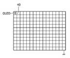
도 3은 전체 화면을 개략적으로 도시한 것으로, 도전 패턴을 접지한 상태를 도시한 평면도,3 is a schematic view of an entire screen and a plan view showing a state in which a conductive pattern is grounded;
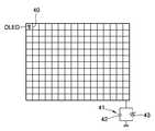
도 4는 전체 화면을 개략적으로 도시한 것으로, 도전 패턴을 접지한 상태를 도시한 평면도.4 is a schematic plan view of an entire screen, and a plan view illustrating a state in which a conductive pattern is grounded;
<도면의 주요 부분에 대한 부호의 설명><Explanation of symbols for the main parts of the drawings>
10: 기판11: 버퍼층10: substrate 11: buffer layer
12: 활성층13: 게이트 절연막12: active layer 13: gate insulating film
14: 게이트 전극16: 층간 절연막14: gate electrode 16: interlayer insulating film
17: 소스 전극18: 드레인 전극17: source electrode 18: drain electrode
20: 절연막21: 화소 정의막20: insulating film 21: pixel defining film
30: 화소 전극31: 유기 발광막30
32: 대향 전극40: 도전 패턴32: counter electrode 40: conductive pattern
41: 전압 유지회로43: 제노 다이오드41: voltage holding circuit 43: xenodiode
본 발명은 평판 표시 장치에 관한 것으로서, 보다 상세하게는 정전기를 방지할 수 있도록 구조가 개선된 평판 표시 장치에 관한 것이다.The present invention relates to a flat panel display, and more particularly, to a flat panel display having an improved structure to prevent static electricity.
통상적으로, 평판 표시 장치(flat displat device)는 크게 발광형과 수광형으로 분류할 수 있다. 발광형으로는 평판 음극선관(flat cathode ray tube)과, 플라즈마 디스플레이 패널(plasma display panel)과, 전계 발광 소자(electro luminescent device)와, 발광 다이오드(light emitting diode) 등이 있다. 수광형으로는 액정 디스플레이(liquid crystal display)를 들 수 있다.In general, a flat displat device may be classified into a light emitting type and a light receiving type. The light emitting type includes a flat cathode ray tube, a plasma display panel, an electroluminescent device, a light emitting diode, and the like. As a light receiving type, a liquid crystal display is mentioned.
이러한 평판 표시장치에 있어서는, 통상, 각 화소마다 패터닝된 화소전극이 구비되며, 액티브 매트릭스형의 경우, 이 화소 전극에 선택 구동회로가 연결된다. 이 선택 구동회로는 하나 이상의 TFT와, 데이터를 저장할 수 있는 하나 이상의 스토리지 커패시터를 구비한다.In such a flat panel display, a patterned pixel electrode is usually provided for each pixel, and in the case of an active matrix type, a selection driving circuit is connected to the pixel electrode. The selection driving circuit includes one or more TFTs and one or more storage capacitors capable of storing data.
그런데, 상기 스토리지 커패시터가 외부의 정전기에 의해 대전될 경우, 화상이 변형되어 원하지 않는 얼룩이 나타나거나, 손상을 받을 수 있다.However, when the storage capacitor is charged by external static electricity, the image may be deformed and unwanted stains may appear or be damaged.
이러한 현상은 유기 전계 발광 표시장치에 특히 많이 나타나는 데, LCD의 경우에는 TFT가 형성된 기판이 액정을 중심으로 디스플레이 표면의 반대측에 위치하고, 디스플레이 표면에는 컬러 필터가 형성된 기판이 배치되어 있어, 외부의 대전(정전기)에 상대적으로 둔감할 수 있으나, 유기 전계 발광 표시장치의 경우, 디스플 레이 표면으로부터 커패시터 전극까지의 거리가 짧아 외부 정전기에 매우 민감하게 된다.This phenomenon is particularly common in organic electroluminescent displays. In the case of LCDs, a substrate on which a TFT is formed is located on the opposite side of the display surface centered on the liquid crystal, and a substrate on which a color filter is formed is disposed on the display surface. Although it may be relatively insensitive to (electrostatic), an organic light emitting display device has a short distance from the surface of the display to the capacitor electrode, making it very sensitive to external static electricity.
본 발명은 상기와 같은 문제점을 해결하기 위한 것으로서, 외부 정전기로부터 화소를 보호할 수 있는 평판 표시 장치를 제공하는데 그 목적이 있다.SUMMARY OF THE INVENTION An object of the present invention is to provide a flat panel display device that can protect a pixel from external static electricity.
상기과 같은 목적을 달성하기 위하여, 본 발명은, 기판과, 상기 기판 상에 형성된 복수개의 화소 전극과, 상기 화소 전극과 절연되도록 기판 상에 형성된 도전 패턴을 포함하는 것을 특징으로 하는 평판 표시 장치를 제공한다.In order to achieve the above object, the present invention provides a flat panel display device comprising a substrate, a plurality of pixel electrodes formed on the substrate, and a conductive pattern formed on the substrate so as to be insulated from the pixel electrodes. do.
이하에서, 첨부된 도면을 참조하면서 본 발명의 바람직한 실시예에 따른 평판 표시 장치를 상세하게 설명하고자 한다.Hereinafter, a flat panel display device according to an exemplary embodiment of the present invention will be described in detail with reference to the accompanying drawings.
도 1은 본 발명의 바람직한 일 실시예에 따른 평판 표시장치를 개략적으로 도시한 것으로, 유기 전계 발광 표시장치의 일부 화소를 도시한 것이다.FIG. 1 schematically illustrates a flat panel display according to an exemplary embodiment of the present invention, and illustrates some pixels of an organic light emitting display.
도 2는 도 1의 화소를 포함한 일부 화소들의 평면도이며, 도 3 및 도 4는 전체 화면을 개략적으로 도시한 평면도이다.2 is a plan view of some pixels including the pixel of FIG. 1, and FIGS. 3 and 4 are plan views schematically illustrating an entire screen.
도 1을 참조하면, 상기 유기 전계 발광 표시장치의 각 화소들은 적, 녹, 청색의 화소(pixel)들이 반복하여 배치되도록 구비되어 있으며, 이러한 화소들의 구성은 반드시 이에 한정되는 것은 아니며, 각 색상의 화소들이 모자이크, 격자상등 다양한 패턴으로 배열될 수 있다. 이러한 화소들은 유기 전계 발광 표시장치의 표 시 영역(미도시)에 복수개가 배열되어 소정의 화상을 구현하게 되고, 표시 영역의 각 화소들은 도 1에서 볼 수 있는 바와 같은 TFT, 커패시터(Cst) 등을 갖는 선택 구동 회로와, 발광 소자인 EL 소자(OLED)를 갖는다. 표시 영역의 외측으로는 도시되지는 않았으나, 각종 구동 회로와, 외부 전원 및 전자 부품들과 연결되는 단자들이 위치한다. 이 표시 영역은 외기와 차단되도록 밀봉된다.Referring to FIG. 1, each pixel of the organic light emitting display device is provided such that red, green, and blue pixels are repeatedly arranged, and the configuration of the pixels is not limited thereto. The pixels may be arranged in various patterns such as a mosaic or a grid. These pixels are arranged in a display area (not shown) of the organic light emitting display device to implement a predetermined image, and each pixel of the display area is a TFT, a capacitor (Cst), etc. as shown in FIG. And a selective driving circuit having a light emitting element and an EL element OLED which is a light emitting element. Although not shown outside the display area, various driving circuits and terminals connected to external power sources and electronic components are positioned. This display area is sealed to block outside air.
여기서, 도 1은 유기 전계 발광 표시 장치의 일 구동 단위인 적, 녹, 청색의 화소들중 어느 한 화소에 대해 확대 도시한 것이다.1 is an enlarged view of one of red, green, and blue pixels as one driving unit of an organic light emitting display device.
상기 TFT는 반드시 도 1에 도시된 구조로만 가능한 것은 아니며, 그 수와 구조는 다양하게 변형 가능하다. 이러한 능동 구동형 유기 전계 발광 소자를 보다 상세히 설명하면 다음과 같다.The TFT is not necessarily possible only with the structure shown in FIG. 1, and the number and structure can be variously modified. The active driving organic electroluminescent device will be described in more detail as follows.
도 1에서 볼 수 있듯이, 글라스 기판(10)상에 버퍼층(11)이 형성되어 있고, 이 버퍼층(11) 상부로 전술한 TFT가 구비된다.As shown in Fig. 1, a
기판(10)은 투명한 글라스재가 사용될 수 있는 데, 이 외에도, 아크릴, 폴리이미드, 폴리카보네이트, 폴리에스테르, 미라르(mylar) 기타 플라스틱 재료가 사용될 수 있다. 물론, 이 외에도 불투명한 소재가 사용될 수도 있다.
버퍼층(11)은 기판(10)으로부터의 불순원소의 침투를 차단하기 위하여, SiO2 및/또는 SiNx 등으로 이루질 수 있는 데, 반드시 이에 한정되는 것은 아니며, 무기막과 유기막이 반복 적층되어 수분침투를 차단하는 베리어층으로 형성될 수 있다.The
상기 TFT는 버퍼층(11) 상에 형성된 활성층(12)과, 이 활성층(12)의 상부에 형성된 게이트 절연막(13)과, 게이트 절연막(13) 상부의 게이트 전극(14)과, 활성 층(12)의 소스/드레인 영역에 접촉되는 소스 전극(17) 및 드레인 전극(18)을 갖는다.The TFT includes an
상기 활성층(12)은 비정질 실리콘 박막 또는 다결정질 실리콘 박막으로 형성될 수 있으나, 반드시 이에 한정되는 것은 아니며, 유기 반도체도 사용 가능하다. 이 반도체 활성층은 소스 및 드레인 영역을 갖는다.The
상기 활성층(12)의 상부에는 SiO2 및/또는 SiNx, 및 기타 절연성 소재 등에 의해 게이트 절연막(13)이 구비되고, 게이트 절연막(13) 상부의 소정 영역에는 MoW, Al/Cu, 기타 도전성 폴리머 등의 도전막으로 게이트 전극(14)이 형성된다. 상기 게이트 전극(14)은 TFT 온/오프 신호를 인가하는 게이트 라인과 연결되어 있다. 그리고, 상기 게이트 전극(14)이 형성되는 영역은 활성층(12)의 채널 영역에 대응된다.The
상기 게이트 전극(12)의 상부로는 층간 절연막(inter-insulator:16)이 형성되고, 층간 절연막(16) 상에는 소스 전극(17) 및 드레인 전극(18)이 형성된다. 소스 전극(17)과 드레인 전극(18)은 각각 층간 절연막(16)에 형성된 컨택 홀을 통해 활성층(12)의 소스 영역 및 드레인 영역에 접하도록 한다.An inter-insulator: 16 is formed on the
소스 및 드레인 전극(17)(18) 상부로는 절연막(20)이 형성된다. 이 절연막(20)은 SiO2 및/또는 SiNx 등의 무기물로 얇게 형성된 후, 아크릴, 폴리 이미드 등의 유기물로 형성될 수 있다. 그러나, 반드시 이에 한정되는 것은 아니며, 유기물 또는 무기물 단일층 구조로 형성될 수도 있다.An
한편, 상기 TFT에는 적어도 하나의 커패시터(Cst)가 연결되는 데, 커패시터 (Cst)의 한 전극(15)은 게이트 전극(14)과 동일층에 형성되고, 다른 한 전극(19)은 TFT의 소스 전극(17)에 연결될 수 있다. 이러한 커패시터의 구조는 반드시 이에 한정되는 것은 아니며, 다양하게 변형 가능함은 물론이다.At least one capacitor Cst is connected to the TFT, wherein one
한편, 상기 드레인 전극(18)에 유기 전계 발광 소자(OLED)가 연결되는 데, 상기 유기 전계 발광 소자(OLED)의 애노우드 전극이 되는 화소 전극(30)에 연결된다. 상기 화소 전극(30)은 절연막(20)의 상부에 형성되어 있고, 그 상부로는 절연성 화소정의막(21)이 형성되어 있으며, 이 화소정의막(21)에 소정의 개구부(22)를 형성한 후, 유기 발광막(31)을 형성한다.Meanwhile, an organic light emitting diode OLED is connected to the
상기 유기 전계 발광 소자(OLED)는 전류의 흐름에 따라 적, 녹, 청색의 빛을 발광하여 소정의 화상 정보를 표시하는 것으로, TFT의 드레인 전극(18)에 연결되어 이로부터 플러스 전원을 공급받는 화소 전극(30)과, 전체 화소를 덮도록 구비되어 마이너스 전원을 공급하는 대향 전극(32), 및 이들 화소 전극(30)과 대향 전극(32)의 사이에 배치되어 발광하는 유기 발광막(31)으로 구성된다.The organic light emitting diode (OLED) emits red, green, and blue light according to the flow of current to display predetermined image information, and is connected to the
상기 유기 발광막(31)은 저분자 또는 고분자 유기층이 사용될 수 있는 데, 저분자 유기 발광막을 사용할 경우 홀 주입층(HIL: Hole Injection Layer), 홀 수송층(HTL: Hole Transport Layer), 발광층(EML: Emission Layer), 전자 수송층(ETL: Electron Transport Layer), 전자 주입층(EIL: Electron Injection Layer) 등이 단일 혹은 복합의 구조로 적층되어 형성될 수 있으며, 사용 가능한 유기 재료도 구리 프탈로시아닌(CuPc: copper phthalocyanine), N,N-디(나프탈렌-1-일)-N,N'-디페닐-벤지딘 (N,N'-Di(naphthalene-1-yl)-N,N'-diphenyl-benzidine: NPB) , 트리스-8-하이드록시퀴놀린 알루미늄(tris-8-hydroxyquinoline aluminum)(Alq3) 등을 비롯해 다양하게 적용 가능하다. 이들 저분자 유기층은 진공증착의 방법으로 형성된다.The organic
고분자 유기 발광막의 경우에는 대개 홀 수송층(HTL) 및 발광층(EML)으로 구비된 구조를 가질 수 있으며, 이 때, 상기 홀 수송층으로 PEDOT를 사용하고, 발광층으로 PPV(Poly-Phenylenevinylene)계 및 폴리플루오렌(Polyfluorene)계 등 고분자 유기물질을 사용하며, 이를 스크린 인쇄나 잉크젯 인쇄방법 등으로 형성할 수 있다.In the case of the polymer organic light emitting film, it may have a structure generally provided with a hole transporting layer (HTL) and a light emitting layer (EML). Polymeric organic materials such as ore (Polyfluorene) are used and can be formed by screen printing or inkjet printing.
상기 화소 전극(30)은 애노우드 전극의 기능을 하고, 상기 대향 전극(32)은 캐소오드 전극의 기능을 한다. 물론, 이들 화소 전극(30)과 대향 전극(32)의 극성은 반대로 되어도 무방하다.The
상기 화소 전극(30)은 투명 전극 또는 반사형 전극으로 구비될 수 있다. 투명전극으로 사용될 때에는 ITO, IZO, ZnO, 또는 In2O3로 구비될 수 있고, 반사형 전극으로 사용될 때에는 Ag, Mg, Al, Pt, Pd, Au, Ni, Nd, Ir, Cr, 및 이들의 화합물 등으로 반사막을 형성한 후, 그 위에 ITO, IZO, ZnO, 또는 In2O3를 형성할 수 있다.The
상기 대향 전극(32)도 투명 전극 또는 반사형 전극으로 구비될 수 있는데, 투명전극으로 사용될 때에는 이 대향 전극(32)이 캐소드 전극으로 사용되므로, 일함수가 작은 금속 즉, Li, Ca, LiF/Ca, LiF/Al, Al, Mg, 및 이들의 화합물이 유기 발광막(31)의 방향을 향하도록 증착한 후, 그 위에 ITO, IZO, ZnO, 또는 In2O3 등 의 투명 전극 형성용 물질로 보조 전극층이나 버스 전극 라인을 형성할 수 있다. 그리고, 반사형 전극으로 사용될 때에는 위 Li, Ca, LiF/Ca, LiF/Al, Al, Mg, 및 이들의 화합물을 전면 증착하여 형성한다.The
상술한 바와 같이, 기판(10) 상에 형성된 유기 전계 발광 표시장치는, 별도의 대향부재(미도시)에 의해 밀봉된다. 대향부재는 기판(10)과 동일하게 글라스 또는 플라스틱재로 구비될 수 있는 데, 이 외에도, 메탈 캡(metal cap) 등으로 형성될 수도 있다. 뿐만 아니라, 상기 기판(10)은 별도의 무기막/유기막의 단일 또는 복합물질에 의해 코팅되어 밀봉될 수도 있다.As described above, the organic light emitting display device formed on the
한편, 본 발명에서 상기 평탄화막(20) 상에는 별도의 도전 패턴(40)이 더 형성된다. 이 도전 패턴(40)은 화소 전극(30)과 동일한 층에 화소 전극(30)과 동일한 물질로 형성될 수 있는 데, 반드시 이에 한정되는 것은 아니며, 다양한 층에 형성될 수 있다.Meanwhile, in the present invention, a separate
상기 도전 패턴(40)은 화소 전극(30)과는 절연되도록 소정 간격 이격될 수 있으며, 도 2에서 볼 수 있듯이, 메쉬(mesh)형태로 형성될 수 있다.The
이러한 도전 패턴(40)을 화소 전극(30)과 동일 물질로 형성할 때에, 화소 전극(30)이 단일층일 경우 단일층으로 형성될 수 있지만, 화소 전극(30)이 전술한 바와 같이 반사형 전극 구조로 형성될 경우에는 그중 어느 한 층만이 도전 패턴(40)에 채용될 수 있다.When the
이러한 도전 패턴(40)은 도 3에서 볼 수 있듯이, 전체 화소의 도전 패턴(40)이 연결되어 접지될 수 있고, 도 4에서 볼 수 있듯이, 제노 다이오드(43)를 포함하 는 전압 유지 회로(41)에 연결될 수 있다.As shown in FIG. 3, the
전압 유지 회로(41)는 제노 다이오드(43)와 제노 다이오드(43)에 병렬로 연결된 커패시터(42)를 포함할 수 있는 데, 반드시 이에 한정되는 것은 아니며, 다양한 종류의 전압 유지 회로(41)가 적용 가능하다.The
이러한 접지 또는 전압 유지 회로(41)에 의해 도전 패턴(40)은 일정한 정전압 상태가 되며, 이에 따라, 정전기에 의한 화상 일그러짐을 방지할 수 있다.By the ground or the
상기 도전 패턴(40)에는 흑색 안료를 첨가하거나, 흑색 처리를 하여 콘트라스트를 향상시키도록 할 수도 있다.A black pigment may be added or the black treatment may be performed to the
이상 설명한 본 발명은 반드시 유기 전계 발광 표시장치에만 적용될 것은 아니며, 액정 표시장치, 무기 전계 발광 표시장치, 및 전자 방출 표시장치 등 다양한 평판 표시장치에 그대로 적용될 수 있음은 물론이다.The present invention described above is not necessarily applied only to an organic light emitting display device, but may be applied to various flat panel display devices such as a liquid crystal display, an inorganic electroluminescent display, and an electron emission display.
이상의 설명에서와 같이 본 발명의 평판 표시 장치에 의하면, 정전기에 의한 화상 일그러짐을 방지할 수 있다.As described above, according to the flat panel display of the present invention, image distortion due to static electricity can be prevented.
또한, 도전 패턴을 흑색 처리함으로써 콘트라스트를 향상시킬 수 있다.Moreover, contrast can be improved by black-processing a conductive pattern.
본 발명은 도면에 도시된 일 실시예를 참고로 설명되었으나 이는 예시적인 것에 불과하며, 본 기술 분야의 통상의 지식을 가진 자라면 이로부터 다양한 변형 및 균등한 타 실시예가 가능하다는 점을 이해할 것이다. 따라서, 본 발명의 진정한 기술적 보호 범위는 첨부된 등록청구범위의 기술적 사상에 의해 정해져야 할 것이다.Although the present invention has been described with reference to one embodiment shown in the drawings, this is merely exemplary, and those skilled in the art will understand that various modifications and equivalent other embodiments are possible therefrom. Therefore, the true technical protection scope of the present invention will be defined by the technical spirit of the appended claims.
Claims (7)
Translated fromKoreanPriority Applications (1)
| Application Number | Priority Date | Filing Date | Title |
|---|---|---|---|
| KR1020040086129AKR100669740B1 (en) | 2004-10-27 | 2004-10-27 | Flat panel display |
Applications Claiming Priority (1)
| Application Number | Priority Date | Filing Date | Title |
|---|---|---|---|
| KR1020040086129AKR100669740B1 (en) | 2004-10-27 | 2004-10-27 | Flat panel display |
Publications (2)
| Publication Number | Publication Date |
|---|---|
| KR20060037026A KR20060037026A (en) | 2006-05-03 |
| KR100669740B1true KR100669740B1 (en) | 2007-01-16 |
Family
ID=37145041
Family Applications (1)
| Application Number | Title | Priority Date | Filing Date |
|---|---|---|---|
| KR1020040086129AExpired - LifetimeKR100669740B1 (en) | 2004-10-27 | 2004-10-27 | Flat panel display |
Country Status (1)
| Country | Link |
|---|---|
| KR (1) | KR100669740B1 (en) |
Cited By (2)
| Publication number | Priority date | Publication date | Assignee | Title |
|---|---|---|---|---|
| WO2010065835A3 (en)* | 2008-12-05 | 2010-09-16 | E. I. Du Pont De Nemours And Company | Backplane structures for solution processed electronic devices |
| WO2010065823A3 (en)* | 2008-12-05 | 2010-09-16 | E. I. Du Pont De Nemours And Company | Backplane structures for solution processed electronic devices |
Families Citing this family (1)
| Publication number | Priority date | Publication date | Assignee | Title |
|---|---|---|---|---|
| CN115951512B (en)* | 2022-12-28 | 2025-07-15 | 广州华星光电半导体显示技术有限公司 | Display Panel |
- 2004
- 2004-10-27KRKR1020040086129Apatent/KR100669740B1/ennot_activeExpired - Lifetime
Cited By (2)
| Publication number | Priority date | Publication date | Assignee | Title |
|---|---|---|---|---|
| WO2010065835A3 (en)* | 2008-12-05 | 2010-09-16 | E. I. Du Pont De Nemours And Company | Backplane structures for solution processed electronic devices |
| WO2010065823A3 (en)* | 2008-12-05 | 2010-09-16 | E. I. Du Pont De Nemours And Company | Backplane structures for solution processed electronic devices |
Also Published As
| Publication number | Publication date |
|---|---|
| KR20060037026A (en) | 2006-05-03 |
Similar Documents
| Publication | Publication Date | Title |
|---|---|---|
| US7510891B2 (en) | Organic light emitting display device and method of manufacturing the same | |
| KR100615212B1 (en) | Flat panel display | |
| CN1577413B (en) | Flat panel display | |
| KR100553745B1 (en) | Flat Panel Display | |
| US8941133B2 (en) | Organic light-emitting display apparatus and method of manufacturing the same | |
| US20040263072A1 (en) | Flat panel display | |
| KR20110049578A (en) | Organic electroluminescent display | |
| US9269756B2 (en) | Organic light emitting display apparatus | |
| US7326966B2 (en) | Electroluminescence display device and method of manufacturing the same | |
| KR100626015B1 (en) | Flat panel display panel and flat panel display device having same | |
| KR101156444B1 (en) | Organic light emitting device and method for manufacturing the same | |
| KR100669740B1 (en) | Flat panel display | |
| KR100813841B1 (en) | Organic light emitting display device | |
| KR100719537B1 (en) | Flat panel displays and substrates for flat panel displays | |
| KR100647611B1 (en) | Flat panel display | |
| KR100615248B1 (en) | Flat panel display | |
| KR100573138B1 (en) | Flat panel display | |
| KR100719599B1 (en) | Flat panel display device | |
| KR100544122B1 (en) | Organic EL display device and manufacturing method thereof | |
| KR100787458B1 (en) | Organic light emitting display device | |
| KR100528914B1 (en) | Organic electro luminescence display device | |
| KR100615256B1 (en) | Flat panel display device | |
| KR100730222B1 (en) | Flat panel display device | |
| JP4770523B2 (en) | Method for manufacturing light emitting device | |
| KR100719556B1 (en) | Flexible printed circuit board and flat panel display device having same |
Legal Events
| Date | Code | Title | Description |
|---|---|---|---|
| A201 | Request for examination | ||
| PA0109 | Patent application | Patent event code:PA01091R01D Comment text:Patent Application Patent event date:20041027 | |
| PA0201 | Request for examination | ||
| PG1501 | Laying open of application | ||
| E902 | Notification of reason for refusal | ||
| PE0902 | Notice of grounds for rejection | Comment text:Notification of reason for refusal Patent event date:20060627 Patent event code:PE09021S01D | |
| E701 | Decision to grant or registration of patent right | ||
| PE0701 | Decision of registration | Patent event code:PE07011S01D Comment text:Decision to Grant Registration Patent event date:20061228 | |
| GRNT | Written decision to grant | ||
| PR0701 | Registration of establishment | Comment text:Registration of Establishment Patent event date:20070110 Patent event code:PR07011E01D | |
| PR1002 | Payment of registration fee | Payment date:20070111 End annual number:3 Start annual number:1 | |
| PG1601 | Publication of registration | ||
| PR1001 | Payment of annual fee | Payment date:20091229 Start annual number:4 End annual number:4 | |
| PR1001 | Payment of annual fee | Payment date:20110103 Start annual number:5 End annual number:5 | |
| PR1001 | Payment of annual fee | Payment date:20111216 Start annual number:6 End annual number:6 | |
| FPAY | Annual fee payment | Payment date:20130102 Year of fee payment:7 | |
| PR1001 | Payment of annual fee | Payment date:20130102 Start annual number:7 End annual number:7 | |
| FPAY | Annual fee payment | Payment date:20140102 Year of fee payment:8 | |
| PR1001 | Payment of annual fee | Payment date:20140102 Start annual number:8 End annual number:8 | |
| FPAY | Annual fee payment | Payment date:20141231 Year of fee payment:9 | |
| PR1001 | Payment of annual fee | Payment date:20141231 Start annual number:9 End annual number:9 | |
| FPAY | Annual fee payment | Payment date:20151230 Year of fee payment:10 | |
| PR1001 | Payment of annual fee | Payment date:20151230 Start annual number:10 End annual number:10 | |
| FPAY | Annual fee payment | Payment date:20170102 Year of fee payment:11 | |
| PR1001 | Payment of annual fee | Payment date:20170102 Start annual number:11 End annual number:11 | |
| FPAY | Annual fee payment | Payment date:20180102 Year of fee payment:12 | |
| PR1001 | Payment of annual fee | Payment date:20180102 Start annual number:12 End annual number:12 | |
| FPAY | Annual fee payment | Payment date:20190102 Year of fee payment:13 | |
| PR1001 | Payment of annual fee | Payment date:20190102 Start annual number:13 End annual number:13 | |
| FPAY | Annual fee payment | Payment date:20191223 Year of fee payment:14 | |
| PR1001 | Payment of annual fee | Payment date:20191223 Start annual number:14 End annual number:14 | |
| PR1001 | Payment of annual fee | Payment date:20210104 Start annual number:15 End annual number:15 | |
| PR1001 | Payment of annual fee | Payment date:20211228 Start annual number:16 End annual number:16 | |
| PR1001 | Payment of annual fee | Payment date:20221226 Start annual number:17 End annual number:17 | |
| PC1801 | Expiration of term | Termination date:20250427 Termination category:Expiration of duration |