KR100669720B1 - Flat panel display device - Google Patents
Flat panel display deviceDownload PDFInfo
- Publication number
- KR100669720B1 KR100669720B1KR1020040061947AKR20040061947AKR100669720B1KR 100669720 B1KR100669720 B1KR 100669720B1KR 1020040061947 AKR1020040061947 AKR 1020040061947AKR 20040061947 AKR20040061947 AKR 20040061947AKR 100669720 B1KR100669720 B1KR 100669720B1
- Authority
- KR
- South Korea
- Prior art keywords
- electrode
- gate
- capacitor
- semiconductor layer
- gate electrode
- Prior art date
- Legal status (The legal status is an assumption and is not a legal conclusion. Google has not performed a legal analysis and makes no representation as to the accuracy of the status listed.)
- Expired - Lifetime
Links
Images


Classifications
- H—ELECTRICITY
- H10—SEMICONDUCTOR DEVICES; ELECTRIC SOLID-STATE DEVICES NOT OTHERWISE PROVIDED FOR
- H10D—INORGANIC ELECTRIC SEMICONDUCTOR DEVICES
- H10D86/00—Integrated devices formed in or on insulating or conducting substrates, e.g. formed in silicon-on-insulator [SOI] substrates or on stainless steel or glass substrates
- H10D86/40—Integrated devices formed in or on insulating or conducting substrates, e.g. formed in silicon-on-insulator [SOI] substrates or on stainless steel or glass substrates characterised by multiple TFTs
- H10D86/441—Interconnections, e.g. scanning lines
- H—ELECTRICITY
- H10—SEMICONDUCTOR DEVICES; ELECTRIC SOLID-STATE DEVICES NOT OTHERWISE PROVIDED FOR
- H10D—INORGANIC ELECTRIC SEMICONDUCTOR DEVICES
- H10D86/00—Integrated devices formed in or on insulating or conducting substrates, e.g. formed in silicon-on-insulator [SOI] substrates or on stainless steel or glass substrates
- H10D86/40—Integrated devices formed in or on insulating or conducting substrates, e.g. formed in silicon-on-insulator [SOI] substrates or on stainless steel or glass substrates characterised by multiple TFTs
- H10D86/60—Integrated devices formed in or on insulating or conducting substrates, e.g. formed in silicon-on-insulator [SOI] substrates or on stainless steel or glass substrates characterised by multiple TFTs wherein the TFTs are in active matrices
- H—ELECTRICITY
- H10—SEMICONDUCTOR DEVICES; ELECTRIC SOLID-STATE DEVICES NOT OTHERWISE PROVIDED FOR
- H10K—ORGANIC ELECTRIC SOLID-STATE DEVICES
- H10K59/00—Integrated devices, or assemblies of multiple devices, comprising at least one organic light-emitting element covered by group H10K50/00
- H10K59/10—OLED displays
- H10K59/12—Active-matrix OLED [AMOLED] displays
- H10K59/121—Active-matrix OLED [AMOLED] displays characterised by the geometry or disposition of pixel elements
- H10K59/1213—Active-matrix OLED [AMOLED] displays characterised by the geometry or disposition of pixel elements the pixel elements being TFTs
- H—ELECTRICITY
- H10—SEMICONDUCTOR DEVICES; ELECTRIC SOLID-STATE DEVICES NOT OTHERWISE PROVIDED FOR
- H10K—ORGANIC ELECTRIC SOLID-STATE DEVICES
- H10K59/00—Integrated devices, or assemblies of multiple devices, comprising at least one organic light-emitting element covered by group H10K50/00
- H10K59/10—OLED displays
- H10K59/12—Active-matrix OLED [AMOLED] displays
- H10K59/131—Interconnections, e.g. wiring lines or terminals
Landscapes
- Engineering & Computer Science (AREA)
- Microelectronics & Electronic Packaging (AREA)
- Physics & Mathematics (AREA)
- Geometry (AREA)
- Devices For Indicating Variable Information By Combining Individual Elements (AREA)
- Electroluminescent Light Sources (AREA)
- Thin Film Transistor (AREA)
- Liquid Crystal (AREA)
Abstract
Translated fromKoreanDescription
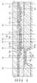
Translated fromKorean도 1은 종래의 인버티드 코플래나형(inverted coplanar type) 박막 트랜지스터를 개략적으로 도시하는 단면도.1 is a cross-sectional view schematically showing a conventional inverted coplanar type thin film transistor.
도 2는 본 발명의 바람직한 또 다른 일 실시예에 따른 능동 구동형 전계발광 디스플레이 장치의 회로를 개략적으로 도시하는 회로도.2 is a circuit diagram schematically showing a circuit of an active driven electroluminescent display device according to another preferred embodiment of the present invention.
도 3은 도 2의 A부분을 도시하는 회로도.3 is a circuit diagram showing portion A of FIG. 2;
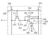
도 4는 도 2 및 도 3의 A부분을 개략적으로 도시하는 능동 구동형 전계발광 디스플레이 장치의 평면도.4 is a plan view of an active driven electroluminescent display device schematically showing part A of FIGS. 2 and 3.
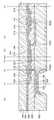
도 5는 상기 실시예에 따른 능동 구동형 전계발광 디스플레이 장치의 부화소부를 도 4의 P1 내지 P8을 따라 취하여 개략적으로 도시하는 단면도.FIG. 5 is a schematic cross-sectional view of a subpixel unit of the active driving type electroluminescent display device according to the embodiment taken along P1 to P8 of FIG. 4.
도 6은 본 발명의 바람직한 또 다른 실시예에 따른 능동 구동형 전계발광 디스플레이 장치의 부화소부를 개략적으로 도시하는 단면도.6 is a schematic cross-sectional view of a subpixel unit of an active driving type electroluminescent display device according to another preferred embodiment of the present invention.
도 7은 본 발명의 바람직한 또 다른 실시예에 따른 능동 구동형 전계발광 디스플레이 장치의 부화소부를 개략적으로 도시하는 단면도.FIG. 7 is a schematic cross-sectional view of a subpixel unit of an active driving type electroluminescent display device according to another preferred embodiment of the present invention. FIG.
도 8은 본 발명의 바람직한 또 다른 실시예에 따른 능동 구동형 전계발광 디스플레이 장치의 부화소부를 개략적으로 도시하는 단면도.8 is a schematic cross-sectional view of a subpixel unit of an active driving type electroluminescent display device according to another preferred embodiment of the present invention.
도 9는 본 발명의 바람직한 또 다른 실시예에 따른 능동 구동형 전계발광 디 스플레이 장치의 부화소부를 개략적으로 도시하는 단면도.Fig. 9 is a sectional view schematically showing a subpixel portion of an active driven electroluminescent display device according to another preferred embodiment of the present invention.
도 10은 본 발명의 바람직한 또 다른 실시예에 따른 능동 구동형 전계발광 디스플레이 장치의 부화소부를 개략적으로 도시하는 단면도.FIG. 10 is a schematic cross-sectional view of a subpixel unit of an active driving type electroluminescent display device according to another preferred embodiment of the present invention. FIG.
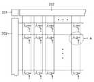
도 11은 본 발명의 바람직한 또 다른 실시예에 따른 능동 구동형 전계발광 디스플레이 장치를 개략적으로 도시하는 평면도.Fig. 11 is a plan view schematically showing an active driven electroluminescent display device according to another preferred embodiment of the present invention.
<도면의 주요부분에 대한 부호의 설명><Description of the symbols for the main parts of the drawings>
311 : 제 2 게이트 전극 312 : 제 3 전극311: second gate electrode 312: third electrode
313 : 제 4 전극 340 : 스토리지 커패시터313: fourth electrode 340: storage capacitor
341 : 제 1 커패시터 전극 342 : 제 2 커패시터 전극341: first capacitor electrode 342: second capacitor electrode
351 : 제 1 게이트 전극 352 : 제 1 전극351: first gate electrode 352: first electrode
353 : 제 2 전극 360 : 표시부353: second electrode 360: display unit
361 : 화소 전극 362 : 대향 전극361: pixel electrode 362: counter electrode
381 : 기판 383 : 게이트 절연막381: substrate 383: gate insulating film
380 : 반도체층 385 : 보호막380: semiconductor layer 385: protective film
385a : 컨택홀 385b : 제 1 컨택홀385a:
385c : 제 2 컨택홀 386 : 화소 정의막385c: second contact hole 386: pixel defining layer
387 : 중간층387: middle layer
본 발명은 평판 디스플레이 장치에 관한 것으로서, 더 상세하게는 크로스 토크가 최소화된 트랜지스터를 구비한 평판 디스플레이 장치에 관한 것이다.BACKGROUND OF THE INVENTION 1. Field of the Invention The present invention relates to a flat panel display device, and more particularly, to a flat panel display device having a transistor with minimum cross talk.
도 1은 종래의 인버티드 코플래나형(inverted coplanar type) 박막 트랜지스터를 개략적으로 도시하는 단면도이다.1 is a schematic cross-sectional view of a conventional inverted coplanar type thin film transistor.
도 1을 참조하면, 기판(81) 상에 게이트 전극(11, 51)이 구비되어 있고, 그 상부에 소스 전극(12, 52) 및 드레인 전극(13, 53)이 구비되어 있으며, 상기 소스 전극(12, 52) 및 드레인 전극(13, 53)을 상기 게이트 전극(11, 51)으로부터 절연시키기 위해 그 사이에 게이트 절연막(83)이 개재되어 있다. 그리고 상기 소스 전극(12, 52) 및 드레인 전극(13, 53)에 각각 접하는 반도체층(80)이 구비되어 있다. 물론 상기 소스 전극(12, 52)과 드레인 전극(13, 53)은 서로 뒤바뀔 수도 있다.Referring to FIG. 1,
상기와 같은 구조에 있어서, 상기 반도체층(80)이 패터닝되어 있지 않고 인접한 두 개의 박막 트랜지스터들(10, 50)에 있어서 일체로 구비되어 있다. 이러한 경우 누설 전류 등으로 인해 인접한 박막 트랜지스터들이 서로 영향을 줄 수 있는 등 소위 크로스 토크가 발생할 수 있으므로, 이를 방지하기 위해 상기 반도체층을 각 박막 트랜지스터 단위로 패터닝하는 것이 좋다. 그러나 상기 반도체층(80)으로 유기 반도체층(organic semiconductor layer)을 이용한 유기 박막 트랜지스터의 경우, 상기 유기 반도체층을 패터닝하는 것은 매우 어려우며, 상기 유기 반도체층이 패터닝되더라도 상기 유기 반도체층의 전기적 특성이 매우 좋지 않게 된다는 문제점이 있다.In the above structure, the
본 발명은 상기와 같은 문제점을 포함하여 여러 문제점들을 해결하기 위한 것으로서, 크로스 토크가 최소화된 트랜지스터를 구비한 평판 디스플레이 장치를 제공하는 것을 목적으로 한다.SUMMARY OF THE INVENTION The present invention has been made to solve various problems including the above problems, and an object of the present invention is to provide a flat panel display device having a transistor with minimized cross talk.
상기와 같은 목적 및 그 밖의 여러 목적을 달성하기 위하여, 본 발명은, 기판과, 상기 기판의 상부에 구비된 제 1 게이트 전극과, 상기 제 1 게이트 전극과 절연되는 제 1 전극과, 상기 제 1 게이트 전극과 절연되고 상기 제 1 전극을 동일 평면에서 감싸는 제 2 전극과, 상기 제 1 게이트 전극과 절연되고 상기 제 1 전극 및 상기 제 2 전극에 접하는 반도체층, 그리고 상기 제 1 전극 및 상기 제 2 전극 중 어느 한 전극에 전기적으로 연결된 화소 전극을 구비하는 디스플레이 소자를 구비하는 것을 특징으로 하는 평판 디스플레이 장치를 제공한다.In order to achieve the above object and various other objects, the present invention provides a substrate, a first gate electrode provided on the substrate, a first electrode insulated from the first gate electrode, and the first A second electrode insulated from the gate electrode and surrounding the first electrode in the same plane, a semiconductor layer insulated from the first gate electrode and in contact with the first electrode and the second electrode, and the first electrode and the second electrode Provided is a flat panel display device comprising a display element having a pixel electrode electrically connected to any one of the electrodes.
이러한 본 발명의 다른 특징에 의하면, 상기 제 1 전극 및 상기 제 2 전극은 상기 제 1 게이트 전극의 상부에 구비되는 것으로 할 수 있다.According to another aspect of the present invention, the first electrode and the second electrode may be provided on the upper portion of the first gate electrode.
본 발명의 또 다른 특징에 의하면, 상기 제 1 게이트 전극은 상기 제 1 전극 및 상기 제 2 전극 사이의 영역에 대응되도록 구비되는 것으로 할 수 있다.According to another feature of the invention, the first gate electrode may be provided so as to correspond to the region between the first electrode and the second electrode.
본 발명의 또 다른 특징에 의하면, 상기 제 1 전극은 제 1 드레인 전극이고 상기 제 2 전극은 제 1 소스 전극이며, 상기 화소 전극에 연결된 전극은 상기 제 1 전극인 것으로 할 수 있다.According to another feature of the present invention, the first electrode may be a first drain electrode, the second electrode may be a first source electrode, and an electrode connected to the pixel electrode may be the first electrode.
본 발명의 또 다른 특징에 의하면, 상기 제 1 게이트 전극에 연결되는 제 1 커패시터 전극과, 상기 제 2 전극에 연결되는 제 2 커패시터 전극을 더 구비하는 것으로 할 수 있다.According to another feature of the invention, it may be further provided with a first capacitor electrode connected to the first gate electrode, and a second capacitor electrode connected to the second electrode.
본 발명의 또 다른 특징에 의하면, 상기 제 1 커패시터 전극과 상기 제 1 게이트 전극은 일체로 구비되며, 상기 제 2 커패시터 전극과 상기 제 2 전극은 일체로 구비되는 것으로 할 수 있다.According to another feature of the present invention, the first capacitor electrode and the first gate electrode may be integrally provided, and the second capacitor electrode and the second electrode may be integrally provided.
본 발명의 또 다른 특징에 의하면, 제 2 게이트 전극과, 상기 제 2 게이트 전극과 절연되는 제 3 전극과, 상기 제 2 게이트 전극과 절연되고 상기 제 3 전극을 감싸는 제 4 전극, 그리고 상기 제 2 게이트 전극과 절연되고 상기 제 3 전극 및 상기 제 4 전극에 접하는 반도체층을 더 구비하고, 상기 제 3 전극 및 상기 제 4 전극 중 어느 한 전극이 상기 제 1 게이트 전극에 전기적으로 연결된 것으로 할 수 있다.According to another feature of the present invention, a second gate electrode, a third electrode insulated from the second gate electrode, a fourth electrode insulated from the second gate electrode and surrounding the third electrode, and the second And a semiconductor layer insulated from the gate electrode and in contact with the third electrode and the fourth electrode, wherein any one of the third electrode and the fourth electrode is electrically connected to the first gate electrode. .
본 발명의 또 다른 특징에 의하면, 상기 제 3 전극 및 상기 제 4 전극은 상기 제 2 게이트 전극의 상부에 구비되는 것으로 할 수 있다.According to still another feature of the present invention, the third electrode and the fourth electrode may be provided above the second gate electrode.
본 발명의 또 다른 특징에 의하면, 상기 제 2 게이트 전극은 상기 제 3 전극 및 상기 제 4 전극 사이의 영역에 대응되도록 구비되는 것으로 할 수 있다.According to another feature of the present invention, the second gate electrode may be provided to correspond to a region between the third electrode and the fourth electrode.
본 발명의 또 다른 특징에 의하면, 상기 제 3 전극이 제 2 드레인 전극이고, 상기 제 4 전극이 제 2 소스 전극이며, 상기 제 1 게이트 전극에 전기적으로 연결된 전극은 상기 제 3 전극인 것으로 할 수 있다.According to another feature of the present invention, the third electrode may be a second drain electrode, the fourth electrode is a second source electrode, and the electrode electrically connected to the first gate electrode may be the third electrode. have.
본 발명의 또 다른 특징에 의하면, 상기 제 1 게이트 전극, 상기 제 2 게이트 전극 및 상기 제 1 커패시터 전극을 덮도록 상기 기판의 전면에 게이트 절연막 이 더 구비되고, 상기 제 1 전극 내지 상기 제 4 전극, 상기 제 2 커패시터 전극 및 상기 반도체층을 덮도록 상기 기판의 전면에 보호막이 더 구비되는 것으로 할 수 있다.According to another feature of the invention, a gate insulating film is further provided on the front surface of the substrate to cover the first gate electrode, the second gate electrode and the first capacitor electrode, the first electrode to the fourth electrode A protective film may be further provided on the entire surface of the substrate to cover the second capacitor electrode and the semiconductor layer.
본 발명의 또 다른 특징에 의하면, 상기 반도체층은 상기 제 1 전극 내지 상기 제 4 전극의 상부에 구비되고, 상기 제 3 전극과 상기 제 1 커패시터 전극은, 상기 제 3 전극의 일부가 노출되도록 상기 보호막 및 상기 반도체층에 구비된 제 1 컨택홀과, 상기 제 1 커패시터 전극의 일부가 노출되도록 상기 보호막과 상기 반도체층과 상기 게이트 절연막에 구비된 제 2 컨택홀과, 상기 보호막 상부에 걸쳐 구비된 배선으로 연결된 것으로 할 수 있다.According to another feature of the invention, the semiconductor layer is provided on the first electrode to the fourth electrode, the third electrode and the first capacitor electrode, the portion so that a portion of the third electrode is exposed A first contact hole provided in the passivation layer and the semiconductor layer, a second contact hole provided in the passivation layer, the semiconductor layer and the gate insulating layer so that a portion of the first capacitor electrode is exposed, and an upper portion of the passivation layer It can be connected by wiring.
본 발명의 또 다른 특징에 의하면, 상기 제 3 전극과 상기 제 1 커패시터 전극을 연결하는 배선은, 상기 게이트 절연막에 구비되는 제 2 컨택홀을 통해 상기 제 1 커패시터 전극에 연결되고 상기 게이트 절연막 상에 구비되며 상기 제 4 전극과 동일한 재료로 형성되는 금속층을 더 구비하는 것으로 할 수 있다.According to another feature of the invention, the wiring connecting the third electrode and the first capacitor electrode is connected to the first capacitor electrode through a second contact hole provided in the gate insulating film and on the gate insulating film And a metal layer formed of the same material as that of the fourth electrode.
본 발명의 또 다른 특징에 의하면, 상기 제 1 전극 내지 상기 제 4 전극은 상기 반도체층의 상부에 구비되고, 상기 제 3 전극과 상기 제 1 커패시터 전극은, 상기 제 3 전극의 일부가 노출되도록 상기 보호막에 구비된 제 1 컨택홀과, 상기 제 1 커패시터 전극의 일부가 노출되도록 상기 보호막과 상기 반도체층과 상기 게이트 절연막에 구비된 제 2 컨택홀과, 상기 보호막 상부에 걸쳐 구비된 배선으로 연결된 것으로 할 수 있다.According to another feature of the invention, the first electrode to the fourth electrode is provided on the upper portion of the semiconductor layer, the third electrode and the first capacitor electrode, the portion so that a part of the third electrode is exposed A first contact hole provided in the passivation layer, a second contact hole provided in the semiconductor layer and the gate insulating layer so that a portion of the first capacitor electrode is exposed, and a wiring provided over the passivation layer. can do.
본 발명의 또 다른 특징에 의하면, 상기 제 3 전극과 상기 제 1 커패시터 전 극을 연결하는 배선은, 상기 게이트 절연막 및 상기 반도체층에 구비되는 제 2 컨택홀을 통해 상기 제 1 커패시터 전극에 연결되고 상기 반도체층 상에 구비되며 상기 제 4 전극과 동일한 재료로 형성되는 금속층을 더 구비하는 것으로 할 수 있다.According to another feature of the invention, the wiring connecting the third electrode and the first capacitor electrode is connected to the first capacitor electrode through the second contact hole provided in the gate insulating film and the semiconductor layer It may be provided with a metal layer provided on the semiconductor layer and formed of the same material as the fourth electrode.
본 발명의 또 다른 특징에 의하면, 상기 화소 전극은 상기 보호막 상에 구비되며, 상기 제 3 전극과 상기 제 1 커패시터 전극을 연결하는 배선은 상기 화소 전극과 동일한 재료로 형성된 것으로 할 수 있다.According to another feature of the present invention, the pixel electrode may be provided on the passivation layer, and the wiring connecting the third electrode and the first capacitor electrode may be formed of the same material as the pixel electrode.
본 발명의 또 다른 특징에 의하면, 상기 제 3 전극이 제 2 소스 전극이고, 상기 제 4 전극이 제 2 드레인 전극이며, 상기 제 1 게이트 전극에 전기적으로 연결된 전극은 상기 제 4 전극인 것으로 할 수 있다.According to another feature of the present invention, the third electrode may be a second source electrode, the fourth electrode is a second drain electrode, and the electrode electrically connected to the first gate electrode may be the fourth electrode. have.
본 발명의 또 다른 특징에 의하면, 상기 제 1 게이트 전극, 상기 제 2 게이트 전극, 상기 제 1 전극 내지 제 4 전극, 상기 제 1 커패시터 전극, 상기 제 2 커패시터 전극 및 상기 반도체층을 덮도록 상기 기판의 전면에 보호막을 더 구비하고, 상기 화소 전극은 상기 보호막 상에 구비되는 것으로 할 수 있다.According to another feature of the invention, the substrate to cover the first gate electrode, the second gate electrode, the first electrode to the fourth electrode, the first capacitor electrode, the second capacitor electrode and the semiconductor layer A protective film may be further provided on the entire surface of the substrate, and the pixel electrode may be provided on the protective film.
본 발명의 또 다른 특징에 의하면, 제 2 게이트 전극과, 상기 제 2 게이트 전극과 절연되는 제 3 전극과, 상기 제 2 게이트 전극과 절연되고 상기 제 3 전극을 감싸는 제 4 전극, 그리고 상기 제 2 게이트 전극과 절연되고 상기 제 3 전극 및 상기 제 4 전극에 접하는 반도체층을 더 구비하고, 상기 제 3 전극 및 상기 제 4 전극 중 어느 한 전극이 상기 제 1 게이트 전극에 전기적으로 연결된 것으로 할 수 있다.According to another feature of the present invention, a second gate electrode, a third electrode insulated from the second gate electrode, a fourth electrode insulated from the second gate electrode and surrounding the third electrode, and the second And a semiconductor layer insulated from the gate electrode and in contact with the third electrode and the fourth electrode, wherein any one of the third electrode and the fourth electrode is electrically connected to the first gate electrode. .
본 발명의 또 다른 특징에 의하면, 상기 제 3 전극 및 상기 제 4 전극은 상 기 제 2 게이트 전극의 상부에 구비되는 것으로 할 수 있다.According to another feature of the invention, the third electrode and the fourth electrode may be provided on the upper portion of the second gate electrode.
본 발명의 또 다른 특징에 의하면, 상기 제 2 게이트 전극은 상기 제 3 전극 및 상기 제 4 전극 사이의 영역에 대응되도록 구비되는 것으로 할 수 있다.According to another feature of the present invention, the second gate electrode may be provided to correspond to a region between the third electrode and the fourth electrode.
본 발명의 또 다른 특징에 의하면, 상기 제 3 전극이 제 2 드레인 전극이고, 상기 제 4 전극이 제 2 소스 전극이며, 상기 제 1 게이트 전극에 전기적으로 연결된 전극은 상기 제 3 전극인 것으로 할 수 있다.According to another feature of the present invention, the third electrode may be a second drain electrode, the fourth electrode is a second source electrode, and the electrode electrically connected to the first gate electrode may be the third electrode. have.
본 발명의 또 다른 특징에 의하면, 상기 제 3 전극이 제 2 소스 전극이고, 상기 제 4 전극이 제 2 드레인 전극이며, 상기 제 1 게이트 전극에 전기적으로 연결된 전극은 상기 제 4 전극인 것으로 할 수 있다.According to another feature of the present invention, the third electrode may be a second source electrode, the fourth electrode is a second drain electrode, and the electrode electrically connected to the first gate electrode may be the fourth electrode. have.
본 발명의 또 다른 특징에 의하면, 상기 반도체층은 유기 반도체층인 것으로 할 수 있다.According to still another feature of the present invention, the semiconductor layer can be an organic semiconductor layer.
본 발명의 또 다른 특징에 의하면, 상기 디스플레이 소자에서 방출되는 광은 상기 기판의 반대 방향으로 출사되는 것으로 할 수 있다.According to another feature of the invention, the light emitted from the display element may be emitted in the opposite direction of the substrate.
본 발명의 또 다른 특징에 의하면, 상기 디스플레이 소자는 전계발광 소자인 것으로 할 수 있다.According to still another feature of the present invention, the display element may be an electroluminescent element.
이하, 첨부된 도면들을 참조하여 본 발명의 바람직한 실시예를 상세히 설명하면 다음과 같다.Hereinafter, exemplary embodiments of the present invention will be described in detail with reference to the accompanying drawings.
전술한 바와 같이, 반도체층, 특히 유기 반도체층이 패터닝되어 있지 않고 인접한 두 개 이상의 박막 트랜지스터들에 있어서 일체로 구비될 경우, 누설 전류 등으로 인해 인접한 박막 트랜지스터들이 서로 영향을 줄 수 있는 등 소위 크로스 토크가 발생할 수 있다는 문제점이 있다. 본 발명에서는 이를 방지하기 위하여, 각각의 박막 트랜지스터의 소스 전극 및 드레인 전극의 구조에 있어서, 일 전극이 타 전극을 동일 평면에서 감싸는 구조의 박막 트랜지스터를 구비한 평판 디스플레이 장치를 제안한다.As described above, when the semiconductor layer, in particular, the organic semiconductor layer is not patterned and integrally provided in two or more adjacent thin film transistors, adjacent thin film transistors may affect each other due to leakage current, etc. There is a problem that torque may occur. In order to prevent this, in the structure of the source electrode and the drain electrode of each thin film transistor, a flat panel display device having a thin film transistor having a structure in which one electrode surrounds the other electrode in the same plane is proposed.
이러한 본 발명의 바람직한 제 1 실시예에 따른 평판 디스플레이 장치를 보다 상세히 설명하자면, 먼저 기판 상부에 제 1 게이트 전극이 구비되고, 상기 제 1 게이트 전극과 절연되는 제 1 전극과, 상기 제 1 게이트 전극과 절연되고 상기 제 1 전극을 동일 평면에서 감싸는 제 2 전극이 구비된다. 상기 제 1 전극 및 상기 제 2 전극은 각각 드레인 전극 또는 소스 전극이 될 수 있다. 그리고 상기 제 1 게이트 전극과 절연되고 상기 제 1 전극 및 상기 제 2 전극에 접하는 반도체층, 그리고 상기 제 1 전극 및 상기 제 2 전극 중 어느 한 전극에 전기적으로 연결된 화소 전극을 구비하는 디스플레이 소자가 구비된다. 특히 상기 반도체층은 유기 반도체층으로 구비될 수 있다. 이때, 상기 게이트 전극은, 상기 제 1 전극과, 상기 제 1 전극을 동일 평면에서 감싸는 상기 제 2 전극 사이의 공간에 대응되도록 구비될 수 있다.The flat panel display device according to the first exemplary embodiment of the present invention will be described in detail. First, a first gate electrode is provided on an upper portion of a substrate, and a first electrode insulated from the first gate electrode, and the first gate electrode. And a second electrode which is insulated from and encloses the first electrode in the same plane. The first electrode and the second electrode may be a drain electrode or a source electrode, respectively. And a display device including a semiconductor layer insulated from the first gate electrode and in contact with the first electrode and the second electrode, and a pixel electrode electrically connected to any one of the first electrode and the second electrode. do. In particular, the semiconductor layer may be provided as an organic semiconductor layer. In this case, the gate electrode may be provided to correspond to a space between the first electrode and the second electrode surrounding the first electrode in the same plane.
상기와 같은 구조에 있어서, 상기 게이트 전극에 의한 채널은 상기 제 1 전극 및 동일 평면에서 이를 감싸고 있는 제 2 전극 사이에만 형성되며, 더욱이 상기 제 1 전극 및 이를 동일 평면에서 감싸고 있는 제 2 전극 사이에서만 전류가 흐르기 때문에, 상기 반도체층이 패터닝되어 있지 않더라도 인접한 박막 트랜지스터들간의 크로스 토크를 방지할 수 있다.In the above structure, the channel by the gate electrode is formed only between the first electrode and the second electrode surrounding it in the same plane, moreover, only between the first electrode and the second electrode surrounding it in the same plane. Since current flows, crosstalk between adjacent thin film transistors can be prevented even if the semiconductor layer is not patterned.
한편, 상기와 같은 구조의 박막 트랜지스터에 있어서, 상기 반도체층이 상기 제 1 전극 및 이를 동일 평면에서 감싸는 제 2 전극의 상부에 구비된 인버티드 코플래나형 박막 트랜지스터가 될 수도 있고, 이와 달리 상기 반도체층이 상기 제 1 전극 및 상기 제 2 전극의 하부에 구비된 인버티드 스태거드형 박막 트랜지스터가 구비될 수도 있는 등, 박막 트랜지스터의 소스 전극 및 드레인 전극 중 일 전극이 타 전극을 동일 평면에서 감싸는 구조를 취하고만 있다면, 어떠한 구조의 박막 트랜지스터도 될 수 있음은 물론이다.Meanwhile, in the thin film transistor having the above structure, the semiconductor layer may be an inverted coplanar thin film transistor provided on the first electrode and the second electrode surrounding the same plane. One of the source electrode and the drain electrode of the thin film transistor may surround the other electrode in the same plane, such as an inverted staggered thin film transistor having a layer provided below the first electrode and the second electrode. Of course, it can be a thin film transistor of any structure as long as it takes.
한편, 상기 제 1 게이트 전극은, 상기 제 1 전극 및 상기 제 1 전극을 동일 평면에서 감싸고 있는 상기 제 2 전극 사이에 대응하는 부분에만 구비되도록, 즉 상기 제 1 게이트 전극의 가운데 부분이 비어있는 도넛 형태로 구비되도록 할 수 있다. 이는 상기 제 1 게이트 전극이 도넛 형태가 아니라, 상기 제 1 전극 및 동일 평면에서 상기 제 1 전극을 감싸고 있는 상기 제 2 전극 사이에 대응하는 부분 외에, 상기 제 1 전극에 대응하는 부분에도 구비된다면, 상기 제 1 전극과 상기 제 1 게이트 전극 간에 기생 커패시턴스가 발생할 수도 있기 때문이다. 따라서, 상기 제 1 게이트 전극은 상기 제 1 전극 및 동일 평면에서 상기 제 1 전극을 감싸고 있는 상기 제 2 전극 사이에 대응하는 부분에만 구비되도록, 즉 상기 제 1 게이트 전극의 가운데 부분이 비어있는 도넛 형태로 구비되도록 하는 것이 좋다.On the other hand, the first gate electrode is provided only in a portion corresponding to between the first electrode and the second electrode surrounding the first electrode in the same plane, that is, a donut in which the center portion of the first gate electrode is empty It may be provided in the form. If the first gate electrode is not in a donut shape, but is also provided in a portion corresponding to the first electrode in addition to a portion corresponding to the first electrode and the second electrode surrounding the first electrode in the same plane, This is because parasitic capacitance may occur between the first electrode and the first gate electrode. Accordingly, the first gate electrode is provided only in a portion corresponding to the first electrode and the second electrode surrounding the first electrode in the same plane, that is, a donut shape in which the center portion of the first gate electrode is empty. It is good to be provided with.
상기와 같은 구조의 박막 트랜지스터 및 이에 연결된 디스플레이 소자를 구비한 평판 디스플레이 장치에 있어서, 상기 디스플레이 소자는 박막 트랜지스터에 연결되어 구동되는 것이라면 어떠한 디스플레이 소자도 될 수 있는바, 예컨대 전계 발광 소자 또는 액정 소자 등을 들 수 있다.In the flat panel display device having the thin film transistor having the above structure and a display element connected thereto, the display element may be any display element connected to the thin film transistor and driven, for example, an electroluminescent element or a liquid crystal element. Can be mentioned.
본 발명에 따른 평판 디스플레이 장치는 특히 전계발광 디스플레이 장치가 될 수 있는 바, 그와 같은 구조의 평판 디스플레이 장치를 설명하자면 다음과 같다.In particular, the flat panel display apparatus according to the present invention may be an electroluminescent display apparatus, and the flat panel display apparatus having such a structure will be described below.
전계발광 디스플레이 장치는 발광층에서의 발광 색상에 따라 다양한 화소 패턴을 구비하는데, 예컨대 적색, 녹색 및 청색의 화소를 구비한다. 상기 적색, 녹색 및 청색으로 형성되는 각 부화소는 자발광 소자인 전계발광 소자 및 상기 전계발광 소자에 연결되는 적어도 하나 이상의 박막 트랜지스터를 구비하게 되는데, 상기 박막 트랜지스터는 전술한 바와 같이, 소스 전극 및 드레인 전극 중 일 전극이 타 전극을 동일 평면에서 감싸는 구조의 박막 트랜지스터가 될 수 있으며, 그 경우 전술한 바와 같은 구조로 상기 전계발광 소자에 연결된다.The electroluminescent display device has various pixel patterns according to the color of light emitted from the light emitting layer. For example, the electroluminescent display device includes red, green, and blue pixels. Each of the subpixels formed in the red, green, and blue colors includes an electroluminescent device, which is a self-luminous device, and at least one thin film transistor connected to the electroluminescent device, wherein the thin film transistor includes: a source electrode; One electrode of the drain electrode may be a thin film transistor having a structure surrounding the other electrode in the same plane, and in this case, the electrode is connected to the electroluminescent device in the above-described structure.
상기 전계발광 소자는 전류구동 방식의 발광 소자로서, 상기 소자를 구성하는 양 전극간의 전류 흐름에 따라 적색, 녹색 또는 청색의 빛을 발광하여 소정의 화상을 구현한다. 상기 전계발광 소자의 구성을 간략히 설명하자면, 상기 전계발광 소자는 전술한 바와 같이 박막 트랜지스터의 제 1 전극 또는 제 2 전극 중 어느 한 전극에 연결된 화소 전극과, 전체 화소들을 덮도록 또는 각 화소에 대응되도록 구비된 대향 전극 및 이들 화소 전극과 대향 전극의 사이에 배치되는 적어도 발광층을 포함하는 중간층으로 구성된다. 본 발명은 반드시 상기와 같은 구조로 한정되는 것은 아니며, 다양한 전계발광 디스플레이 장치의 구조가 그대로 적용될 수 있음은 물론이다.The electroluminescent device is a light emitting device of a current driving method, and emits red, green, or blue light according to the flow of current between both electrodes constituting the device to implement a predetermined image. To briefly describe the configuration of the electroluminescent device, the electroluminescent device may include a pixel electrode connected to either one of the first electrode and the second electrode of the thin film transistor and cover all pixels or correspond to each pixel as described above. And an intermediate layer including at least one light emitting layer disposed between the counter electrode and the pixel electrode and the counter electrode. The present invention is not necessarily limited to the above structure, and the structures of various electroluminescent display devices can be applied as it is.
상기 화소 전극은 애노드 전극의 기능을 하고, 상기 대향 전극은 캐소드 전극의 기능을 하는 데, 물론, 이들 화소 전극과 대향 전극의 극성은 반대로 되어도 무방하다.The pixel electrode functions as an anode electrode, and the counter electrode functions as a cathode electrode. Of course, the polarity of these pixel electrodes and the counter electrode may be reversed.
상기 화소 전극은 투명 전극 또는 반사형 전극으로 구비될 수 있는 데, 투명전극으로 사용될 때에는 ITO, IZO, ZnO 또는 In2O3로 구비될 수 있다. 반사형 전극으로 사용될 때에는 Ag, Mg, Al, Pt, Pd, Au, Ni, Nd, Ir, Cr 또는 이들의 화합물 등으로 반사막을 형성한 후, 그 위에 ITO, IZO, ZnO 또는 In2O3로 구비될 수 있다.The pixel electrode may be provided as a transparent electrode or a reflective electrode. When the pixel electrode is used as a transparent electrode, the pixel electrode may be provided as ITO, IZO, ZnO, or In2 O3 . When used as a reflective electrode, a reflective film is formed of Ag, Mg, Al, Pt, Pd, Au, Ni, Nd, Ir, Cr, or a compound thereof, and then ITO, IZO, ZnO or In2 O3 thereon. It may be provided.
상기 대향 전극도 투명 전극 또는 반사형 전극으로 구비될 수 있는데, 투명전극으로 사용될 때에는 Li, Ca, LiF/Ca, LiF/Al, Al, Ag, Mg 또는 이들의 화합물이 상기 중간층을 향하도록 증착한 후, 그 위에 ITO, IZO, ZnO 또는 In2O3 등의 투명 전극 형성용 물질로 보조 전극층이나 버스 전극 라인이 구비되도록 할 수 있다. 그리고 반사형 전극으로 사용될 때에는 상기 Li, Ca, LiF/Ca, LiF/Al, Al, Ag, Mg 또는 이들의 화합물을 전면 증착하여 형성한다. 그러나, 반드시 이에 한정되는 것은 아니며, 화소 전극 및 대향 전극으로 전도성 폴러머 등 유기물을 사용할 수도 있다.The counter electrode may also be provided as a transparent electrode or a reflective electrode. When used as a transparent electrode, Li, Ca, LiF / Ca, LiF / Al, Al, Ag, Mg, or a compound thereof is deposited to face the intermediate layer. Subsequently, an auxiliary electrode layer or a bus electrode line may be provided as a material for forming a transparent electrode such as ITO, IZO, ZnO, or In2 O3 thereon. When used as a reflective electrode, Li, Ca, LiF / Ca, LiF / Al, Al, Ag, Mg, or a compound thereof is formed by full deposition. However, the present invention is not limited thereto, and an organic material such as a conductive polymer may be used as the pixel electrode and the counter electrode.
한편, 상기 중간층이 무기막으로 형성되었는가 유기막으로 형성되었는가에 따라 무기 전계발광 소자와 유기 전계발광 소자로 나뉜다. 후자의 경우, 유기막으로 구비된 중간층으로는 저분자 유기막 또는 고분자 유기막으로 구비될 수 있다.On the other hand, depending on whether the intermediate layer is formed of an inorganic film or an organic film is divided into an inorganic electroluminescent device and an organic electroluminescent device. In the latter case, the intermediate layer provided as the organic film may be provided as a low molecular organic film or a polymer organic film.
저분자 유기막을 사용할 경우, 상기 중간층은 홀 주입층(HIL: hole injection layer), 홀 수송층(HTL: hole transport layer), 발광층(EML: emission layer), 전자 수송층(ETL: electron transport layer) 및 전자 주입층(EIL: electron injection layer) 등이 단일 혹은 복합의 구조로 적층되어 형성될 수 있으며, 사용 가능한 유기 재료도 구리 프탈로시아닌(CuPc: copper phthalocyanine), N,N-디(나프탈렌-1-일)-N,N'-디페닐-벤지딘 (N,N'-Di(naphthalene-1-yl)-N,N'-diphenyl-benzidine: NPB) , 트리스-8-하이드록시퀴놀린 알루미늄(tris-8-hydroxyquinoline aluminum)(Alq3) 등을 비롯해 다양하게 적용 가능하다. 이러한 저분자 유기막은 진공 중에서 유기물을 가열하여 증착하는 방식으로 형성될 수 있다. 물론 상기 중간층의 구조는 반드시 위에 한정되는 것은 아니고, 필요에 따라 다양한 층으로서 구성할 수 있다.When using a low molecular organic film, the intermediate layer may include a hole injection layer (HIL), a hole transport layer (HTL), an emission layer (EML), an electron transport layer (ETL) and an electron injection. A layer (EIL: electron injection layer) may be formed by stacking a single or a complex structure, and the usable organic materials may be copper phthalocyanine (CuPc), N, N-di (naphthalen-1-yl)- N, N'-diphenyl-benzidine (N, N'-Di (naphthalene-1-yl) -N, N'-diphenyl-benzidine: NPB), tris-8-hydroxyquinoline aluminum aluminum) (Alq3), etc. The low molecular weight organic film may be formed by heating and depositing an organic material in a vacuum. Of course, the structure of the said intermediate | middle layer is not necessarily limited to above, It can comprise as various layers as needed.
고분자 유기막을 사용할 경우에는 상기 중간층은 대개 홀 수송층(HTL) 및 발광층(EML)으로 구비될 수 있다. 상기 고분자 홀 수송층은 폴리에틸렌 디히드록시티오펜(PEDOT : poly-(2,4)-ethylene-dihydroxy thiophene)이나, 폴리아닐린(PANI : polyaniline) 등을 사용하여 잉크젯 프린팅이나 스핀 코팅의 방법에 의해 형성될 수 있다. 상기 고분자 유기 발광층은 PPV, Soluble PPV's, Cyano-PPV, 폴리플루오렌(Polyfluorene) 등으로 구비될 수 있으며, 잉크젯 프린팅이나 스핀 코팅 또는 레이저를 이용한 열전사방식 등의 통상의 방법으로 컬러 패턴을 형성할 수 있다. 물론 이러한 고분자 유기층의 경우에도 상기 중간층의 구조는 반드시 위에 한정되는 것은 아니고, 필요에 따라 다양한 층으로서 구성할 수 있다.In the case of using a polymer organic film, the intermediate layer may be provided as a hole transport layer (HTL) and an emission layer (EML). The polymer hole transport layer may be formed by ink jet printing or spin coating using polyethylene dihydroxythiophene (PEDOT: poly- (2,4) -ethylene-dihydroxy thiophene) or polyaniline (PANI: polyaniline). Can be. The polymer organic light emitting layer may be formed of PPV, Soluble PPV's, Cyano-PPV, polyfluorene, or the like, and may form a color pattern by a conventional method such as inkjet printing, spin coating, or thermal transfer using a laser. Can be. Of course, in the case of such a polymer organic layer, the structure of the intermediate layer is not necessarily limited to the above, and may be configured as various layers as necessary.
무기 전계발광 소자의 경우에는 상기 중간층은 무기막으로 구비되며, 이는 발광층 및 상기 발광층과 전극 사이에 개재된 절연층으로 구비될 수 있다. 물론 상기 중간층의 구조는 반드시 위에 한정되는 것은 아니고, 필요에 따라 다양한 층으로서 구성할 수 있다.In the case of an inorganic electroluminescent device, the intermediate layer may be provided as an inorganic layer, which may be provided as an emission layer and an insulating layer interposed between the emission layer and the electrode. Of course, the structure of the said intermediate | middle layer is not necessarily limited to above, It can comprise as various layers as needed.
상기 발광층은 ZnS, SrS, CaS 등과 같은 금속황화물 또는 CaGa2S4, SrGa2S4 등과 같은 알카리 토류 칼륨 황화물, 및 Mn, Ce, Tb, Eu, Tm, Er, Pr, Pb 등을 포함하는 천이 금속 또는 알카리 희토류 금속들과 같은 발광중심원자들로 구비될 수 있다.The light emitting layer is a transition, including ZnS, SrS, metal sulfide orCaGa 2 S 4, SrGa 2 S 4 alkaline-earth potassium sulfide such as such as CaS, and Mn, Ce, Tb, Eu, Tm, Er, Pr, Pb , etc. Light emitting core atoms such as metal or alkaline rare earth metals.
상술한 바와 같은 구조로 이루어진 전계발광 디스플레이 장치는, 상기 전계발광 소자의 화소 전극에, 전술한 것과 같이, 소스 전극 및 드레인 전극 중 일 전극이 타 전극을 동일 평면에서 감싸는 구조의 박막 트랜지스터의 드레인 전극이 연결되어 상기 화소 전극에 유입되는 전류의 흐름을 제어함으로써 각 화소의 발광여부를 제어하게 된다.In the electroluminescent display device having the above-described structure, as described above, one electrode among the source electrode and the drain electrode surrounds the other electrode in the same plane on the pixel electrode of the electroluminescent element. This connection is controlled to control the light emission of each pixel by controlling the flow of current flowing into the pixel electrode.
한편 전술한 바와 같이 액정 디스플레이 패널에도 상기 유기 박막 트랜지스터가 구비될 수 있는 바, 상기 액정 디스플레이 패널의 구조를 간략히 설명하자면 다음과 같다.Meanwhile, as described above, the organic thin film transistor may be provided in the liquid crystal display panel. The structure of the liquid crystal display panel will be briefly described as follows.
서로 대향된 제 1 기판과 제 2 기판 사이에 액정층을 배향하는 배양층들이 구비되고, 상기 배양층과 상기 제 1 기판 사이에는 화소 전극이, 상기 배양층과 제 2 기판 사이에는 대향 전극이 구비되며, 상기 제 2 기판과 상기 대향 전극 사이에는 칼라 필터층이 구비된다. Culture layers for aligning the liquid crystal layer are provided between the first substrate and the second substrate facing each other, a pixel electrode is provided between the culture layer and the first substrate, the opposite electrode is provided between the culture layer and the second substrate A color filter layer is provided between the second substrate and the counter electrode.
상기 제 1 기판의 상기 제 2 기판 방향의 면 반대측 면에는 제 1 편광층이, 상기 제 2 기판의 상기 제 1 기판 방향의 면 반대측 면에는 제 2 편광층이 구비되고, 상기 제 2 편광층의 상면에는 보호필름이 구비된다.The first polarizing layer is provided on the surface opposite the surface of the first substrate in the second substrate direction, and the second polarizing layer is provided on the surface opposite the surface of the second substrate in the first substrate direction. The upper surface is provided with a protective film.
상기와 같은 구조의 액정 패널에 있어서, 상기 화소 전극이, 전술한 바와 같은 소스 전극 및 드레인 전극 중 일 전극이 타 전극을 동일 평면에서 감싸는 구조의 박막 트랜지스터의 드레인 전극에 연결됨으로써, 상기 박막 트랜지스터에 의해 제어된 외부신호에 의해 상기 화소 전극과 상기 대향 전극 사이에 전위차가 형성되고, 상기 전위차에 의해 상기 액정층의 배열이 결정되며, 상기 액정층의 배열에 따라서 상기 액정 패널의 제 1 기판 하부에 구비되는 백라이트 유니트(BLU : back light unit)에서 공급되는 가시광선이 차폐 또는 통과되고, 통과된 광이 상기 칼라 필터층을 통과하면서 색을 띠게 되어 화상을 구현하게 된다.In the liquid crystal panel having the above structure, the pixel electrode is connected to the drain electrode of the thin film transistor structure in which one of the source electrode and the drain electrode as described above surrounds the other electrode in the same plane, thereby providing the thin film transistor. A potential difference is formed between the pixel electrode and the counter electrode by an external signal controlled by the external signal, and the arrangement of the liquid crystal layer is determined by the potential difference, and the lower portion of the liquid crystal panel is disposed below the first substrate according to the arrangement of the liquid crystal layer. Visible light supplied from a back light unit (BLU) provided is shielded or passed through, and the passed light becomes colored while passing through the color filter layer to implement an image.
물론 전술한 본 발명에 따른 박막 트랜지스터는 상기 전계발광 디스플레이 장치나 액정 디스플레이 장치 이외의 다양한 평판 디스플레이 장치에도 구비될 수 있음은 물론이며, 평판 디스플레이 장치 외의 전자 종이(electronic sheet), 스마트 카드(smart card), 상품 태그 또는 RFID 용 플라스틱 칩(smart tag, RFID) 등 박막 트랜지스터를 구비하는 모든 장치에 구비될 수 있음은 물론이다. 이하 후술할 실시예들에 있어서는, 편의상 소스 전극 및 드레인 전극 중 일 전극이 타 전극을 동일 평면에서 감싸는 구조의 박막 트랜지스터에 연결된 디스플레이 소자가 전계발광 소자인 경우에 대해 설명하겠다.Of course, the above-described thin film transistor according to the present invention may be provided in various flat panel display devices other than the electroluminescent display device or the liquid crystal display device, as well as an electronic sheet and a smart card other than the flat panel display device. ), A product tag or a plastic chip for RFID (smart tag, RFID) can be provided in any device having a thin film transistor. In the following embodiments, for convenience, a display device connected to a thin film transistor having a structure in which one of the source electrode and the drain electrode surrounds the other electrode in the same plane will be described as an electroluminescent device.
도 2는 본 발명의 바람직한 제 2 실시예에 따른 능동 구동형 전계발광 디스 플레이 장치의 회로를 개략적으로 도시하는 회로도이고, 도 3은 도 2의 A부분을 도시하는 회로도이며, 도 4는 도 2 및 도 3의 A부분을 개략적으로 도시하는 능동 구동형 전계발광 디스플레이 장치의 평면도이고, 도 5는 상기 실시예에 따른 능동 구동형 전계발광 디스플레이 장치의 부화소부를 도 3의 P1 내지 P8을 따라 취하여 개략적으로 도시하는 단면도이다.FIG. 2 is a circuit diagram schematically showing a circuit of an active driving type electroluminescent display device according to a second preferred embodiment of the present invention, FIG. 3 is a circuit diagram showing part A of FIG. 2, and FIG. 4 is FIG. 3 is a plan view of an active driving type electroluminescent display device schematically showing part A of FIG. 3, and FIG. 5 is a sub-pixel portion of the active driving type electroluminescent display device according to the embodiment, taken along P1 to P8 of FIG. 3. It is sectional drawing which shows schematically.
상기 도면들을 참조하면, 본 발명의 바람직한 제 2 실시예에 따른 평판 디스플레이 장치는 디스플레이 소자를 구동하는, 소스 전극 및 드레인 전극 중 일 전극이 타 전극을 동일 평면에서 감싸는 구조의 제 1 박막 트랜지스터(250), 상기 제 1 박막 트랜지스터(250)에 전기적으로 연결된 커패시터(240), 그리고 상기 제 1 박막 트랜지스터(250)를 구동하는, 소스 전극 및 드레인 전극 중 일 전극이 타 전극을 동일 평면에서 감싸는 구조의 제 2 박막 트랜지스터(210)를 구비한다.Referring to the drawings, a flat panel display device according to a second exemplary embodiment of the present invention includes a first
상기 제 1 박막 트랜지스터(250)는, 기판(281)의 상부에 제 1 게이트 전극(251)을 구비하고, 상기 제 1 게이트 전극(251)과 절연되는 제 1 전극(253)을 구비하며, 상기 제 1 게이트 전극(251)과 절연되고 상기 제 1 전극(253)을 동일 평면에서 감싸는 제 2 전극(252)을 구비한다. 그리고 상기 제 1 게이트 전극(251)과 절연되고 상기 제 1 전극(253) 및 상기 제 2 전극(252)에 접하는 반도체층(280)을 구비한다. 이때 상기 제 1 전극(253) 및 상기 제 2 전극(252) 중 어느 한 전극에 디스플레이 소자의 화소 전극(261)이 연결되며, 도 4 및 도 5에서는 상기 제 1 전극(253)에 상기 화소 전극(261)이 연결되어 있다. 이때 상기 박막 트랜지스터의 제 1 전극(253)은 드레인 전극이 될 수 있고 상기 제 1 전극(253)을 감싸고 있는 상기 제 2 전극(252)은 소스 전극이 될 수 있다. 이하 후술할 실시예들에 있어서는 상기 제 1 전극(253)이 드레인 전극인 경우에 대해 설명한다.The first
도 4를 참조하면, 상기 화소 전극(261)이 상기 제 1 박막 트랜지스터(250), 상기 제 2 박막 트랜지스터(210) 및 상기 스토리지 커패시터(240)가 구비되지 않은 부화소 영역에 구비되어 있는, 즉, 상기 화소 전극(261)에 연결되는 디스플레이 소자에서 발생한 광이 상기 기판(281) 방향으로 취출되는 소위 배면 발광형의 디스플레이 장치에 해당하는 구조를 취하고 있으나, 이는 편의상 상기와 같이 도시한 것이다. 즉, 상기 화소 전극(261)은 도 4에 도시된 것과 달리 상기 제 1 박막 트랜지스터(250), 상기 스토리지 커패시터(240) 및 상기 제 2 박막 트랜지스터(210)의 상부에까지 구비될 수도 있으며, 이는 후술할 실시예들에 있어서도 동일하다.Referring to FIG. 4, the
도 4 및 도 5에서는 반도체층(280)이 제 1 전극(253) 및 제 2 전극(251)의 상부에 구비된 인버티드 코플래나형(inverted coplanar type)의 박막 트랜지스터가 도시되어 있으나, 이와 달리 반도체층(280)이 제 1 전극(253) 및 제 2 전극(251)의 하부에 구비된 인버티드 스태거드형(inverted staggered type) 박막 트랜지스터가 구비될 수도 있다. 후자의 박막 트랜지스터가 구비된 구조에 대해서는 별도의 실시예로서 후술한다.4 and 5 illustrate an inverted coplanar type thin film transistor in which the
한편, 도 4 및 도 5를 참조하면, 상기 제 1 게이트 전극(251)은 상기 제 1 전극(253) 및 상기 제 1 전극(253)을 동일 평면에서 감싸고 있는 상기 제 2 전극(252) 사이에 대응하는 부분에만 구비되도록, 즉 상기 제 1 게이트 전극(251)의 가운데 부분이 비어있는 형태로 구비되어 있다. 이는 상기 제 1 게이트 전극(251)이 도 4 및 도 5에 도시된 바와 같은 도넛 형태가 아니라, 상기 제 1 전극(253) 및 상기 제 1 전극(253)을 동일 평면에서 감싸고 있는 상기 제 2 전극(252) 사이에 대응하는 부분 외에, 상기 제 1 전극(253)에 대응하는 부분에도 구비된다면, 상기 제 1 전극(253)과 상기 제 1 게이트 전극(251) 간에 기생 커패시턴스가 발생할 수도 있기 때문이다. 따라서, 상기 제 1 게이트 전극(251)은 상기 제 1 전극(253) 및 상기 제 1 전극(253)을 동일 평면에서 감싸고 있는 상기 제 2 전극(252) 사이에 대응하는 부분에만 구비되도록, 즉 상기 제 1 게이트 전극(251)의 가운데 부분이 비어있는 형태로 구비되도록 하는 것이 좋다.4 and 5, the
한편, 도 2 내지 도 5를 참조하면, 상기 제 1 박막 트랜지스터(250)에는 스토리지 커패시터(240)가 더 구비될 수 있다. 이에 대해 더 자세히 설명하자면, 상기 스토리지 커패시터(240)는 제 1 커패시터 전극(241) 및 제 2 커패시터 전극(242)으로 구비되는데, 상기 제 1 커패시터 전극(241)은 상기 제 1 게이트 전극(251)에 연결되며, 상기 제 2 커패시터 전극(242)은 상기 제 2 전극(252) 및 제 3 도선(270)에 연결된다.Meanwhile, referring to FIGS. 2 to 5, the first
이때 도 4 및 도 5에 도시된 바와 같이, 상기 제 1 커패시터 전극(241)과 상기 제 1 게이트 전극(251)은 일체로 구비될 수 있으며, 상기 제 2 커패시터 전극(242)과 상기 제 2 전극(252)은 일체로 구비될 수 있다.4 and 5, the
한편, 상기 도면들을 참조하면, 전술한 바와 같이, 본 실시예에 따른 능동 구동형 전계발광 소자를 구비한 평판 디스플레이 장치는 또 하나의 박막 트랜지스터, 특히 소스 전극 및 드레인 전극 중 일 전극이 타 전극을 동일 평면에서 감싸는 구조의 제 2 박막 트랜지스터(210)를 더 구비할 수 있다. 이에 대해 도 4 및 도 5를 참조하여 설명하자면, 제 2 게이트 전극(211)이 구비되고, 상기 제 2 게이트 전극(211)과 절연되는 제 3 전극(213)이 구비되며, 상기 제 2 게이트 전극(211)과 절연되고 상기 제 3 전극(213)을 동일 평면에서 감싸는 제 4 전극(212)을 구비하고, 상기 제 2 게이트 전극(211)과 절연되고 상기 제 3 전극(213) 및 상기 제 4 전극(212)에 접하는 반도체층(280)이 구비된다. 이때 상기 제 3 전극(213) 및 상기 제 4 전극(212) 중 어느 한 전극이 상기 제 1 게이트 전극(251)에 전기적으로 연결되는 바, 도 4 및 도 5에서는 상기 제 3 전극(213)에 연결되어 있다.Meanwhile, referring to the drawings, as described above, in the flat panel display device having the active driving type electroluminescent device according to the present embodiment, one of the thin film transistors, in particular, one of the source electrode and the drain electrode, has the other electrode. A second
상기와 같은 구조에 있어서, 상기 제 3 전극(213) 및 상기 제 4 전극(212)은 상기 제 2 게이트 전극(211)의 상부에 구비되면 되는 바, 이 경우에도 인버티드 코플래나형 또는 인버티드 스태거드형이 될 수 있는 바, 도 5에 도시된 평판 디스플레이 장치에 있어서는 인버티드 코플래나형으로 구비되어 있다. 이는 전술한 제 1 박막 트랜지스터(250)와 동일한 구조를 취하도록 하기 위함이며, 후술하는 실시예에서와 같이 상기 제 1 박막 트랜지스터(250)와 상기 제 2 박막 트랜지스터(210)가 인버티드 스태거드형으로 구비되도록 할 수 있음은 물론이다. 이는 후술한다.In the above structure, the
상술한 바와 같은 구조의 제 2 박막트랜지스터(210)에 있어서도, 전술한 것과 동일한 이유로, 상기 제 2 게이트 전극(211)은 상기 제 3 전극(213) 및 상기 제 4 전극(212) 사이의 영역에 대응되도록 구비될 수 있음은 물론이다. 그리고 상기 제 3 전극(213)과 상기 제 4 전극(212) 중 하나의 전극은 소스 전극이 되고 다른 전극은 드레인 전극이 되는 바, 도 4 및 도 5에는 상기 제 3 전극(213)이 제 2 드 레인 전극이 되고 상기 제 4 전극(212)이 제 2 소스 전극이 되는 구조를 도시하고 있다. 이와 달리, 상기 제 3 전극(213)이 제 2 소스 전극이 되고 상기 제 4 전극(212)이 제 2 드레인 전극이 되는 구조는, 별도의 실시예로서 후술한다.In the second
상기와 같은 구조에 있어서, 상기 제 1 게이트 전극(251), 상기 제 2 게이트 전극(211) 및 상기 제 1 커패시터(241) 전극을 덮도록 상기 기판(281)의 전면에 게이트 절연막(283)이 더 구비되고, 상기 제 1 전극(253) 내지 상기 제 4 전극(212), 상기 제 2 커패시터 전극(242) 및 상기 반도체층(280)을 덮도록 상기 기판(281)의 전면에 보호막(285)이 더 구비되도록 할 수 있다. 이 경우 상기 스토리지 커패시터(240)가 상기 제 1 박막 트랜지스터(250) 및 상기 제 2 박막 트랜지스터(210)에 연결되어 구비되도록 하기 위해서는 컨택홀이 구비되어야 하는 바, 이에 대해 설명한다.In the above structure, a
전술한 바와 같이, 본 실시예에 따른 평판 표시장치의 박막트랜지스터는, 상기 반도체층(280)이 상기 제 1 전극(253) 내지 상기 제 4 전극(212)의 상부에 구비되는 인버티드 코플래나형 박막 트랜지스터인 경우이다. 이때 전술한 바와 같이 상기 제 3 전극(213)과 상기 제 1 커패시터 전극(241)이 서로 연결되는 바, 이를 위해 상기 제 3 전극(213)의 일부가 노출되도록 상기 보호막(285) 및 상기 반도체층(280)에 제 1 컨택홀(285b)이 구비되고, 상기 제 1 커패시터 전극(241)의 일부가 노출되도록 상기 보호막(285), 상기 반도체층(280) 및 상기 게이트 절연막(283)에 제 2 컨택홀(285c)이 구비된다. 상기 제 3 전극(213)과 상기 제 1 커패시터 전극(241)은, 상기 제 1 컨택홀(285b), 상기 제 2 컨택홀(285c), 그리고 상기 보호막 (285) 상부에 걸쳐 구비된 배선으로 연결된다. 이때 상기 제 3 전극(213)과 상기 제 1 커패시터 전극(241)을 연결하는 상기 배선은, 상기 제 1 박막 트랜지스터(250)의 제 1 전극(253), 즉 제 1 드레인 전극에 연결되는 화소 전극(261)을 형성할 때, 상기 화소 전극(261)과 동일 재료로 동시에 형성되도록 할 수 있다.As described above, in the thin film transistor of the flat panel display according to the present exemplary embodiment, an inverted coplanar type in which the
상기와 같은 구조에 있어서, 도 2 내지 도 5를 참조하여 각 구조의 상호관계를 유기적으로 설명한다. 상기 제 2 박막 트랜지스터(210)의 제 4 전극(212)은 제 1 도선(220)에 의하여 구동 회로에 연결되고, 제 2 박막 트랜지스터의 제 2 게이트 전극(211)은 제 2 도선(230)에 의하여 구동 회로에 연결되며, 제 2 박막 트랜지스터의 제 3 전극(213)은 스토리지 커패시터(240)의 제 1 커패시터 전극(241) 및 제 1 박막 트랜지스터(250)의 제 1 게이트 전극(251)에 연결된다. 상기와 같은 구조에 있어서 상기 제 4 전극(212)은 상기 제 2 박막 트랜지스터(210)의 소스 전극이 되며, 상기 제 3 전극(213)은 상기 제 2 박막 트랜지스터(210)의 드레인 전극이 된다. 또한, 상기 제 1 도선(220)이 데이터를 전송하는 데이터 라인(data line), 제 2 도선(130)이 스캔 라인(scan line)에 해당하는 것으로 할 수 있으며, 이 경우 상기 제 2 트랜지스터(210)가 스위칭 트랜지스터(switching TR) 역할을, 상기 제 1 트랜지스터(250)가 드라이빙 트랜지스터(driving TR) 역할을 하게 된다. 물론 상기 선택 구동 회로에 있어서 두 개 이상의 트랜지스터를 사용할 수도 있다. 본 실시예 및 후술할 실시예들에 있어서는 스위칭 트랜지스터와 드라이빙 트랜지스터 두 개의 트랜지스터가 사용된 경우에 대해 설명하겠다.In the above structure, the mutual relationship between the structures will be organically described with reference to FIGS. 2 to 5. The
상기 스토리지 커패시터(240)의 제 2 커패시터 전극(242)과 상기 제 1 박막 트랜지스터(250)의 제 2 전극(252)은 제 3 도선(270)에 연결되고, 상기 제 1 박막 트랜지스터(250)의 제 1 전극(253)은 표시부(260)의 화소 전극(261)에 연결된다. 상기와 같은 구조에 있어서, 상기 제 2 전극(252)은 상기 제 1 박막 트랜지스터(250)의 소스 전극이 되며, 상기 제 1 전극(253)은 상기 제 1 박막 트랜지스터(250)의 드레인 전극이 된다.The
전술한 바와 같이 상기 표시부(260)는 전계발광 소자가 될 수 있는 바, 이 경우 도 5로부터 알 수 있는 바와 같이, 디스플레이 부의 대향 전극(262)은 상기 화소 전극(261)과 소정의 간극을 두고 대향 배치되고, 상기 화소 전극(261)과 상기 대향 전극(262) 사이에는 적어도 발광층을 포함하는 중간층(287)이 구비된다. 상기 화소 전극(261), 대향전극(262), 그리고 그 사이에 개재되는 적어도 발광층을 포함하는 중간층(287)의 구조 및 재료는 전술한 바와 같다.As described above, the
상기와 같은 능동 구동형 전계발광 디스플레이 장치의 작동원리를 간략히 살펴보면 다음과 같다.Briefly look at the operation principle of the active-type electroluminescent display device as described above.
구동회로에 의하여 제 2 게이트 전극(211)에 전압이 인가되면 제 4 전극, 즉 제 2 소스 전극(212)과 제 3 전극, 즉 제 2 드레인 전극(213)을 연결하는 반도체층(280)에 도전 채널이 형성되는데, 이 때 제 1 도선(220)에 의하여, 발광층을 포함하는 중간층(287)에서 발생하는 광량을 결정하는 데이터를 가진 전하가 상기 제 2 소스 전극(212)에 공급되면, 상기 전하가 상기 제 2 드레인 전극(213)으로 이동된다. 그리고 상기 전하는 상기 제 2 드레인 전극(213)을 거쳐 제 1 커패시터 전극(241)에 축적되게 되고, 또한 제 3 도선(270)을 통해 공급된 소정의 전하가 제 2 커패시터 전극(242)에 축적되게 되어, 상기 제 1 커패시터 전극(241)과 상기 제 2 커패시터 전극(242) 양단에, 발광층을 포함하는 중간층(287)에서 발생하는 광량을 결정하는 데이터를 가진 전압이 형성된다. 그리고 상기 전압이 제 1 게이트 전극(251)과 제 2 전극, 즉 제 1 소스 전극(252) 간의 전압이 되어, 상기 제 3 도선(270)을 통해 상기 제 1 소스 전극(252)에 공급된 전하 중 제 1 드레인 전극(253)을 거쳐 표시부, 즉 전계발광 소자(260)의 화소 전극(261)으로 이동하는 전하량, 즉 발광층을 포함하는 중간층(287)에서 발생하는 광량을 결정하는 전하량을 조절하게 된다.When a voltage is applied to the
상술한 바와 같은 구조의 능동 구동형 전계발광 소자에 있어서는 각 부화소별로 드라이빙 트랜지스터 및 스위칭 트랜지스터 등의 복수개의 박막 트랜지스터들이 사용되는 바, 상기와 같은 박막 트랜지스터들에 있어서 크로스 토크가 발생하면 표시부(260)에서의 광량 조절이 제대로 이루어지지 않게 되며, 그 결과 올바른 상을 표현하지 못하게 된다.In the active driving type electroluminescent device having the above-described structure, a plurality of thin film transistors such as a driving transistor and a switching transistor are used for each subpixel. When the cross talk occurs in the thin film transistors, the display unit 260 ), The amount of light is not adjusted properly, and as a result, the correct image cannot be represented.
따라서 전술한 바와 같은, 소스 전극 및 드레인 전극 중 일 전극이 타 전극을 동일 평면에서 감싸는 구조의 박막 트랜지스터를 사용하면, 반도체층을 패터닝하지 않고도 그와 같은 크로스 토크를 방지함으로써, 보다 선명하고 정확한 상을 나타낼 수 있다.Therefore, when using a thin film transistor having a structure in which one of the source electrode and the drain electrode wraps the other electrode in the same plane, the crosstalk is prevented without patterning the semiconductor layer, thereby providing a clearer and more accurate image. Can be represented.
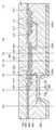
도 6은 본 발명의 바람직한 제 3 실시예에 따른 능동 구동형 전계발광 디스플레이 장치의 부화소부를 개략적으로 도시하는 단면도이다.6 is a cross-sectional view schematically showing a subpixel unit of an active driving type electroluminescent display device according to a third embodiment of the present invention.
본 실시예에 따른 능동 구동형 전계발광 디스플레이 장치가 전술한 제 2 실 시예에 따른 능동 구동형 전계발광 디스플레이 장치와 다른 점은, 제 2 박막 트랜지스터(310)의 제 3 전극(313)과, 스토리지 커패시터(340)의 제 1 커패시터 전극(341)을 연결함에 있어서, 금속층(343)이 더 구비되어 있다는 점이다.The active driving type electroluminescent display device according to the present embodiment differs from the active driving type electroluminescent display device according to the second embodiment described above in that the
전술한 바와 같이 상기 제 3 전극(313)과 상기 제 1 커패시터 전극(341)을 연결하기 위해, 상기 제 3 전극(313)의 일부가 노출되도록 보호막(385) 및 반도체층(380)에 제 1 컨택홀(385b)이 구비되고, 상기 제 1 커패시터 전극(341)의 일부가 노출되도록 상기 보호막(385), 상기 반도체층(380) 및 게이트 절연막(383)에 제 2 컨택홀(385c)이 구비된다. 상기 제 3 전극(313)과 상기 제 1 커패시터 전극(341)은, 상기 제 1 컨택홀(385b), 상기 제 2 컨택홀(385c), 그리고 상기 보호막(385) 상부에 걸쳐 구비된 배선으로 연결된다. 물론 전술한 바와 같이 상기 제 3 전극(313)과 상기 제 1 커패시터 전극(341)을 연결하는 상기 배선은, 제 1 박막 트랜지스터(350)의 제 1 전극(353), 즉 제 1 드레인 전극에 연결되는 화소 전극(361)을 형성할 때, 상기 화소 전극(361)과 동일 재료로 동시에 형성되도록 할 수 있음은 물론이다. 이는 후술할 실시예들에 있어서도 동일하다.As described above, in order to connect the
상기와 같은 형태의 배선으로 상기 제 3 전극(313)과 상기 제 1 커패시터 전극(341)을 연결함에 있어서, 상기 배선과 상기 제 1 커패시터 전극(341)과의 접촉을 확실히 하기 위해, 상기 제 1 커패시터 전극(341)을 덮고 있는 게이트 절연막(383) 상에 구비되며 상기 게이트 절연막(383)에 구비된 제 2 컨택홀(385c)을 통해 상기 제 1 커패시터 전극(341)에 연결되는 금속층(343)이 상기 형태의 배선에 더 구비되도록 할 수 있다. 이 경우 상기 금속층(343)은 제 1 전극(353) 내지 제 4 전 극(312), 그리고 제 2 커패시터 전극(342)을 형성할 때 동시에 동일한 재료로 형성되도록 할 수 있다.In connecting the
상기와 같은 구조를 취함으로써, 상기 제 3 전극(313)과 상기 제 1 커패시터 전극(341)을 연결함에 있어서, 제 2 컨택홀(385c) 내에서 상기 배선이 상기 제 1 커패시터 전극(341)에 접촉되지 않을 수 있는 불량을 방지할 수 있다.By taking the above structure, in connecting the
도 7은 본 발명의 바람직한 제 4 실시예에 따른 능동 구동형 전계발광 디스플레이 장치의 부화소부를 개략적으로 도시하는 단면도이다. 본 실시예에 따른 능동 구동형 전계발광 디스플레이 장치가, 전술한 제 2 실시예에 따른 능동 구동형 전계발광 디스플레이 장치와 다른 점은, 제 1 박막 트랜지스터(450) 및 제 2 박막 트랜지스터(410)가 인버티드 코플래나형이 아닌, 인버티드 스태거드형이라는 것이다. 즉 제 1 전극(453) 내지 제 4 전극(412)이 반도체층(480)의 상부에 구비되어 있다.7 is a schematic cross-sectional view of a subpixel unit of an active driving type electroluminescent display device according to a fourth embodiment of the present invention. The active driving type electroluminescent display device according to the present embodiment differs from the active driving type electroluminescent display device according to the second embodiment described above in that the first thin film transistor 450 and the second thin film transistor 410 Inverted stapled, not inverted coplanar. That is, the
상기와 같이, 반도체층(480)이 각 박막 트랜지스터별로 패터닝되어 있지 않은 인버티드 스태거드형의 박막 트랜지스터를 사용하더라도, 소스 전극 및 드레인 전극 중 일 전극이 타 전극을 동일 평면에서 감싸는 구조의 박막 트랜지스터를 사용하여 도 7에 도시된 바와 같은 구조를 갖도록 함으로써, 크로스 토크를 방지하여 보다 선명하고 정확한 상을 나타낼 수 있다.As described above, even when the
도 8은 본 발명의 바람직한 제 5 실시예에 따른 능동 구동형 전계발광 디스플레이 장치의 부화소부를 개략적으로 도시하는 단면도이다. 본 실시예에 따른 능동 구동형 전계발광 디스플레이 장치는 전술한 제 4 실시예에 따른 능동 구동형 전 계발광 디스플레이 장치와 동일하게 인버티드 스태거드형 박막 트랜지스터를 구비하고 있다. 본 실시예에 따른 능동 구동형 전계발광 디스플레이 장치가 전술한 제 4 실시예에 따른 능동 구동형 전계발광 디스플레이 장치와 다른 점은, 제 2 박막 트랜지스터(510)의 제 3 전극(513)과, 스토리지 커패시터(540)의 제 1 커패시터 전극(541)을 연결함에 있어서, 금속층(543)이 더 구비되어 있다는 점이다.8 is a schematic cross-sectional view of a subpixel unit of an active driving type electroluminescent display device according to a fifth exemplary embodiment of the present invention. The active driving type electroluminescent display device according to the present embodiment includes an inverted staggered thin film transistor in the same manner as the active driving type electroluminescent display device according to the fourth embodiment described above. The active driving type electroluminescent display device according to the present embodiment differs from the active driving type electroluminescent display device according to the fourth embodiment described above in that the
본 실시예에 따른 능동 구동형 전계발광 디스플레이 장치에 있어서도, 상기 제 3 전극(513)과 상기 제 1 커패시터 전극(541)을 연결하기 위해, 상기 제 3 전극(513)의 일부가 노출되도록 보호막(585) 및 반도체층(580)에 제 1 컨택홀(585b)이 구비되고, 상기 제 1 커패시터 전극(541)의 일부가 노출되도록 상기 보호막(585), 상기 반도체층(580) 및 게이트 절연막(583)에 제 2 컨택홀(585c)이 구비된다.Also in the active driving type electroluminescent display device according to the present embodiment, in order to connect the
상기 제 3 전극(513)과 상기 제 1 커패시터 전극(541)은, 상기 제 1 컨택홀(585b), 상기 제 2 컨택홀(585c), 그리고 상기 보호막(585) 상부에 걸쳐 구비된 배선으로 연결되는 것은 전술한 제 4 실시예에 따른 능동 구동형 전계발광 소자와 동일하다.The
본 실시예에서는, 상기와 같은 형태의 배선으로 상기 제 3 전극(513)과 상기 제 1 커패시터 전극(541)을 연결함에 있어서, 상기 배선과 상기 제 1 커패시터 전극(541)과의 접촉을 확실히 하기 위해, 상기 제 1 커패시터 전극(541)을 덮고 있는 반도체층(480) 상에 구비되며, 상기 반도체층(480) 및 그 하부의 게이트 절연막(583)에 구비된 제 2 컨택홀(585c)을 통해 상기 제 1 커패시터 전극(541)에 연결되는 금속층(543)이 상기 형태의 배선에 더 구비되도록 할 수 있다. 이 경우 상기 금 속층(543)은 제 1 전극(553) 내지 제 4 전극(512), 그리고 제 2 커패시터 전극(542)을 형성할 때 동시에 동일한 재료로 형성되도록 할 수 있다.In the present embodiment, in connecting the
상기와 같은 구조를 취함으로써, 상기 제 3 전극(513)과 상기 제 1 커패시터 전극(541)을 연결함에 있어서, 제 2 컨택홀(585c) 내에서 상기 배선이 상기 제 1 커패시터 전극(541)에 접촉되지 않을 수 있는 불량을 방지할 수 있다.By taking the above structure, the wiring is connected to the
도 9는 본 발명의 바람직한 제 6 실시예에 따른 능동 구동형 전계발광 디스플레이 장치의 부화소부를 개략적으로 도시하는 단면도이다.9 is a schematic cross-sectional view of a subpixel unit of an active driving type electroluminescent display device according to a sixth exemplary embodiment of the present invention.
본 실시예에 따른 능동 구동형 전계발광 디스플레이 장치가 전술한 제 2 실시예에 따른 능동 구동형 전계발광 디스플레이 장치와 다른 점은, 제 2 박막 트랜지스터(610)의 소스 전극 및 드레인 전극의 위치가 다르다는 것이다.The active driving electroluminescent display device according to the present embodiment differs from the active driving electroluminescent display device according to the second embodiment described above in that positions of the source electrode and the drain electrode of the second thin film transistor 610 are different. will be.
즉 전술한 제 2 실시예에 있어서는 제 3 전극(213)을 제 4 전극(212)이 감싸고 있으며, 상기 제 3 전극(213)이 드레인 전극, 상기 제 4 전극(212)이 소스 전극이 되어, 상기 제 3 전극(213)이 스토리지 커패시터(240)의 제 1 커패시터 전극(241)에 연결되어 있었다. 그러나 본 실시예에 있어서는, 제 3 전극(613)을 제 4 전극(612)이 감싸고 있는 것은 동일하나, 상기 제 2 실시예와 달리, 상기 제 3 전극(613)이 소스 전극이 되고, 상기 제 4 전극(612)이 드레인 전극이 되며, 상기 제 4 전극(612)이 스토리지 커패시터(640)의 제 1 커패시터 전극(641)에 연결되어 제 1 게이트 전극(651)에 전기적으로 연결되어 있고, 상기 제 3 전극(513)은 제 2 배선(620)에 연결되어 있다.That is, in the above-described second embodiment, the
상기와 같은 구조에 있어서, 상기 제 4 전극(612)과 상기 제 1 커패시터 전 극(641)이 연결되는 바, 전술한 실시예들과 달리 보호막(685) 상부를 거치는 형태의 배선을 사용하지 않고도 상기 제 4 전극(612)과 상기 제 1 커패시터 전극(641)을 연결할 수 있다는 장점이 있다. 또한 전술한 제 3 실시예 및 제 5 실시예에 따른 전계발광 디스플레이 장치들과 달리, 상기 제 4 전극(612)과 상기 제 1 커패시터 전극(641)의 연결에 있어서, 상기 제 1 커패시터 전극(641)에의 연결을 확실하게 하기 위해 금속층을 더 구비할 필요가 없다는 장점이 있다.In the above structure, the
한편, 본 실시예에 다른 능동 구동형 전계발광 디스플레이 장치에서는 반도체층(680)이 제 1 전극(653) 및 제 4 전극(612)의 상부에 구비된 인버티드 코플래나형 박막 트랜지스터를 구비한 디스플레이 장치이나, 물론 도 10에 도시된 본 발명의 바람직한 제 7 실시예에 따른 능동 구동형 전계발광 디스플레이 장치와 같이, 반도체층(780)이 제 1 전극(753) 및 제 4 전극(712)의 하부에 구비된 인버티드 스태거드형 박막 트랜지스터를 구비한 디스플레이 장치에도 본 발명이 적용될 수 있음은 물론이다.On the other hand, in the active driving type electroluminescent display device according to the present embodiment, the
도 11은 본 발명의 바람직한 제 8 실시예에 따른 능동 구동형 전계발광 디스플레이 장치를 개략적으로 도시하는 평면도이다.FIG. 11 is a plan view schematically illustrating an active driving type electroluminescent display device according to an eighth exemplary embodiment of the present invention.
전술한 바와 같이, 반도체층이 패터닝되어 있지 않고 박막 트랜지스터들에 있어서 일체로 구비되어 있을 경우, 누설 전류 등으로 인해 인접한 박막 트랜지스터들이 서로 영향을 줄 수 있는 등 소위 크로스 토크가 발생할 수 있으므로, 이를 방지하기 위해 상기 반도체층을 각 박막 트랜지스터 단위로 패터닝하는 것이 좋다. 그러나 상기 반도체층으로 유기 반도체층(organic semiconductor layer)을 이용한 유기 박막 트랜지스터의 경우, 상기 유기 반도체층을 패터닝하는 것은 매우 어려우며, 상기 유기 반도체층이 패터닝되더라도 상기 유기 반도체층의 전기적 특성이 매우 좋지 않게 된다는 문제점이 있다.As described above, when the semiconductor layer is not patterned and is integrally provided in the thin film transistors, so-called cross talk may occur because adjacent thin film transistors may affect each other due to leakage current or the like, thus preventing this. In order to do this, the semiconductor layer may be patterned in units of thin film transistors. However, in the case of an organic thin film transistor using an organic semiconductor layer as the semiconductor layer, it is very difficult to pattern the organic semiconductor layer, and even if the organic semiconductor layer is patterned, the electrical characteristics of the organic semiconductor layer are very poor. There is a problem.
따라서 본 발명에서는 상기와 같은 문제점을 해결하기 위해, 크로스 토크를 방지할 수 있는, 소스 전극 및 드레인 전극 중 일 전극이 타 전극을 동일 평면에서 감싸는 구조의 박막 트랜지스터를 도입한 평판 디스플레이 장치를 게시하고 있는 바, 이러한 구조의 박막 트랜지스터들간의 크로스 토크 발생 가능성을 더욱 최소화하기 위해, 도 11에 도시된 바와 같이, 제 1 박막 트랜지스터(850)와 제 2 박막 트랜지스터(810)가 더 멀리 떨어져 있도록 할 수 있다. 상기와 같은 구조를 취함으로써, 인접한 박막 트랜지스터들간의 크로스 토크 발생 가능성을 더욱 최소화할 수 있으며, 이를 통해 더욱 정확하고 선명한 상을 구현할 수 있다.Therefore, in order to solve the above problems, the present invention discloses a flat panel display device in which a thin film transistor having a structure in which one of the source electrode and the drain electrode wraps the other electrode in the same plane and prevents cross talk is disclosed. As shown in FIG. 11, the first thin film transistor 850 and the second thin film transistor 810 may be further separated from each other to further minimize the possibility of cross talk between thin film transistors having such a structure. have. By taking the above structure, it is possible to further minimize the possibility of crosstalk between adjacent thin film transistors, thereby realizing a more accurate and clear image.
한편, 도 4 내지 도 11을 참조하면, 소스 전극 및 드레인 전극 중 일 전극이 타 전극을 동일 평면에서 감싸는 구조의 박막 트랜지스터는 종래의 박막 트랜지스터에 비해 차지하는 면적이 크기 때문에, 상기와 같은 구조의 박막 트랜지스터에 연결된 디스플레이 소자에서 발생된 광이 상기 박막 트랜지스터가 구비된 기판의 반대 방향으로 취출되는 전면 발광형일 경우에 그 효용성이 크다고 할 것이나, 본 발명이 반드시 이에 한정되는 것은 아니며, 배면 발광형 또는 양면 발광형에도 적용될 수 있음은 물론이다.Meanwhile, referring to FIGS. 4 to 11, the thin film transistor having a structure in which one electrode of the source electrode and the drain electrode wraps the other electrode in the same plane has a larger area than the conventional thin film transistor, and thus, the thin film having the structure described above When the light generated from the display device connected to the transistor is a top emission type that is extracted in the opposite direction of the substrate provided with the thin film transistor, the usefulness is great, but the present invention is not necessarily limited thereto. Of course, it can be applied to the light emitting type.
한편, 상기 제 2 실시예 내지 제 8 실시예에 있어서, 디스플레이 소자로서 전계발광 소자가 구비되고, 상기 전계발광 소자에 전기적으로 연결되어 상기 전계 발광 소자를 구동시키는 것으로서 두 개의 박막 트랜지스터 및 커패시터가 구비된 구조를 예를 들어 설명하였으나, 본 발명이 이에 한정되는 것은 아니다. 즉, 전술한 바와 같이 디스플레이 소자로서 액정 소자가 구비될 수도 있으며, 그러한 경우에는 하나의 박막 트랜지스터와 하나의 커패시터, 또는 그 이상의 박막 트랜지스터들이 구비될 수도 있고, 커패시터 없이 두 개 또는 그 이상의 박막 트랜지스터들만이 구비될 수도 있는 등, 여러 변형예가 가능함은 물론이다.Meanwhile, in the second to eighth embodiments, an electroluminescent element is provided as a display element, and is electrically connected to the electroluminescent element to drive the electroluminescent element, and includes two thin film transistors and a capacitor. The illustrated structure has been described by way of example, but the present invention is not limited thereto. That is, as described above, a liquid crystal device may be provided as a display device, in which case one thin film transistor and one capacitor, or more thin film transistors may be provided, and only two or more thin film transistors without a capacitor may be provided. Of course, various modifications are possible, such as this may be provided.
상기한 바와 같이 이루어진 본 발명의 평판 디스플레이 장치에 따르면, 다음과 같은 효과를 얻을 수 있다.According to the flat panel display device of the present invention made as described above, the following effects can be obtained.
첫째, 소스 전극 및 드레인 전극 중 일 전극이 타 전극을 동일 평면에서 감싸는 구조의 박막 트랜지스터를 구비한 평판 디스플레이 장치를 통해, 반도체층이 패터닝되지 않은 박막 트랜지스터들간의 크로스 토크를 방지할 수 있다.First, through a flat panel display device having a thin film transistor having a structure in which one electrode of the source electrode and the drain electrode surrounds the other electrode in the same plane, crosstalk between the thin film transistors in which the semiconductor layer is not patterned can be prevented.
둘째, 소스 전극 및 드레인 전극 중 일 전극이 타 전극을 동일 평면에서 감싸는 구조의 박막 트랜지스터의 드레인 전극과 커패시터의 일 전극을 컨택홀들 및 보호막 상부에 걸쳐 구비된 배선으로 연결함에 있어서, 상기 배선에, 상기 커패시터의 일 전극에 연결되는 금속층이 구비되도록 함으로써, 상기 배선과 상기 커패시터의 일 전극과의 접촉을 확실히 할 수 있다.Second, when one of the source electrode and the drain electrode is connected to the drain electrode of the thin film transistor structure of the structure surrounding the other electrode in the same plane and the one electrode of the capacitor by the wiring provided over the contact holes and the protective layer, By providing a metal layer connected to one electrode of the capacitor, it is possible to ensure contact between the wiring and one electrode of the capacitor.
셋째, 박막 트랜지스터의 드레인 전극이 소스 전극을 동일 평면에서 감싸는 구조를 취하도록 함으로써, 상기 드레인 전극과 커패시터의 일 전극과의 연결을 더욱 간단하고 확실하게 할 수 있다.Third, by making the drain electrode of the thin film transistor wrap around the source electrode in the same plane, the connection between the drain electrode and one electrode of the capacitor can be made simpler and more reliable.
본 발명은 도면에 도시된 실시예를 참고로 설명되었으나 이는 예시적인 것에 불과하며, 당해 기술 분야에서 통상의 지식을 가진 자라면 이로부터 다양한 변형 및 균등한 다른 실시예가 가능하다는 점을 이해할 것이다. 따라서, 본 발명의 진정한 기술적 보호 범위는 첨부된 특허청구범위의 기술적 사상에 의하여 정해져야 할 것이다.Although the present invention has been described with reference to the embodiments shown in the drawings, these are merely exemplary, and those skilled in the art will understand that various modifications and equivalent other embodiments are possible. Therefore, the true technical protection scope of the present invention will be defined by the technical spirit of the appended claims.
Claims (26)
Translated fromKoreanPriority Applications (6)
| Application Number | Priority Date | Filing Date | Title |
|---|---|---|---|
| KR1020040061947AKR100669720B1 (en) | 2004-08-06 | 2004-08-06 | Flat panel display device |
| JP2005176803AJP4198131B2 (en) | 2004-08-06 | 2005-06-16 | Flat panel display device |
| US11/187,873US7279714B2 (en) | 2004-08-06 | 2005-07-25 | Flat panel display device |
| EP05107007AEP1624489B1 (en) | 2004-08-06 | 2005-07-29 | Flat panel display device with reduced cross-talk |
| DE602005023694TDE602005023694D1 (en) | 2004-08-06 | 2005-07-29 | Flat screen with reduced crosstalk |
| CN200510091066.7ACN100531501C (en) | 2004-08-06 | 2005-08-05 | Flat panel display device |
Applications Claiming Priority (1)
| Application Number | Priority Date | Filing Date | Title |
|---|---|---|---|
| KR1020040061947AKR100669720B1 (en) | 2004-08-06 | 2004-08-06 | Flat panel display device |
Publications (2)
| Publication Number | Publication Date |
|---|---|
| KR20060013115A KR20060013115A (en) | 2006-02-09 |
| KR100669720B1true KR100669720B1 (en) | 2007-01-16 |
Family
ID=36139920
Family Applications (1)
| Application Number | Title | Priority Date | Filing Date |
|---|---|---|---|
| KR1020040061947AExpired - LifetimeKR100669720B1 (en) | 2004-08-06 | 2004-08-06 | Flat panel display device |
Country Status (6)
| Country | Link |
|---|---|
| US (1) | US7279714B2 (en) |
| EP (1) | EP1624489B1 (en) |
| JP (1) | JP4198131B2 (en) |
| KR (1) | KR100669720B1 (en) |
| CN (1) | CN100531501C (en) |
| DE (1) | DE602005023694D1 (en) |
Families Citing this family (22)
| Publication number | Priority date | Publication date | Assignee | Title |
|---|---|---|---|---|
| KR100796592B1 (en)* | 2005-08-26 | 2008-01-21 | 삼성에스디아이 주식회사 | Thin film transistor and its manufacturing method |
| US8138075B1 (en) | 2006-02-06 | 2012-03-20 | Eberlein Dietmar C | Systems and methods for the manufacture of flat panel devices |
| TWI430234B (en)* | 2006-04-05 | 2014-03-11 | Semiconductor Energy Lab | Semiconductor device, display device, and electronic device |
| KR101540341B1 (en)* | 2008-10-17 | 2015-07-30 | 삼성전자주식회사 | PANEL STRUCTURE, DISPLAY DEVICE COMPRISING PANEL STRUCTURE AND METHOD FOR MANUFACTURING |
| KR20160072845A (en) | 2008-10-24 | 2016-06-23 | 가부시키가이샤 한도오따이 에네루기 켄큐쇼 | Semiconductor device and method for manufacturing the same |
| US8247276B2 (en) | 2009-02-20 | 2012-08-21 | Semiconductor Energy Laboratory Co., Ltd. | Thin film transistor, method for manufacturing the same, and semiconductor device |
| KR101404951B1 (en) | 2009-07-01 | 2014-06-09 | 샤프 가부시키가이샤 | Active matrix substrate and organic el display device |
| WO2011013409A1 (en) | 2009-07-28 | 2011-02-03 | シャープ株式会社 | Active matrix substrate, display device, and organic el display device |
| US8115883B2 (en)* | 2009-08-27 | 2012-02-14 | Semiconductor Energy Laboratory Co., Ltd. | Display device and method for manufacturing the same |
| WO2011048838A1 (en) | 2009-10-20 | 2011-04-28 | シャープ株式会社 | Active matrix substrate and organic el display device |
| KR101094296B1 (en)* | 2010-05-31 | 2011-12-19 | 삼성모바일디스플레이주식회사 | Display device and manufacturing method thereof |
| US9142568B2 (en) | 2010-09-10 | 2015-09-22 | Semiconductor Energy Laboratory Co., Ltd. | Method for manufacturing light-emitting display device |
| DE102011016308A1 (en) | 2011-04-07 | 2012-10-11 | Osram Opto Semiconductors Gmbh | display device |
| US8922464B2 (en)* | 2011-05-11 | 2014-12-30 | Semiconductor Energy Laboratory Co., Ltd. | Active matrix display device and driving method thereof |
| JP6033071B2 (en)* | 2011-12-23 | 2016-11-30 | 株式会社半導体エネルギー研究所 | Semiconductor device |
| US9166054B2 (en)* | 2012-04-13 | 2015-10-20 | Semiconductor Energy Laboratory Co., Ltd. | Semiconductor device and manufacturing method thereof |
| KR101796812B1 (en)* | 2013-02-15 | 2017-11-10 | 엘지디스플레이 주식회사 | Flexible organic light emitting display device and method of manufacturing the same |
| TWI523217B (en)* | 2013-09-12 | 2016-02-21 | 友達光電股份有限公司 | Pixel structure |
| KR20150044324A (en)* | 2013-10-16 | 2015-04-24 | 삼성디스플레이 주식회사 | Thin film transistor array substrate and method thereof |
| KR102124025B1 (en) | 2013-12-23 | 2020-06-17 | 엘지디스플레이 주식회사 | Organic Light Emitting Diode Display Device and Method of Fabricating the Same |
| US9991326B2 (en)* | 2015-01-14 | 2018-06-05 | Panasonic Intellectual Property Management Co., Ltd. | Light-emitting device comprising flexible substrate and light-emitting element |
| KR20230105745A (en)* | 2022-01-04 | 2023-07-12 | 삼성디스플레이 주식회사 | Display Apparatus |
Citations (5)
| Publication number | Priority date | Publication date | Assignee | Title |
|---|---|---|---|---|
| JP2002141511A (en)* | 2000-11-01 | 2002-05-17 | Matsushita Electric Ind Co Ltd | Active matrix liquid crystal display device |
| KR20020079187A (en)* | 2001-04-13 | 2002-10-19 | 삼성에스디아이 주식회사 | Plat panel display device and method for fabricating the same |
| JP2003076299A (en)* | 2001-07-25 | 2003-03-14 | Lg Phillips Lcd Co Ltd | Active matrix organic electroluminescent device with simplified manufacturing process and manufacturing method thereof |
| JP2004191931A (en) | 2002-11-26 | 2004-07-08 | Seiko Epson Corp | Electro-optical device, method of manufacturing the same, and electronic apparatus |
| JP2004193129A (en) | 2002-12-11 | 2004-07-08 | Samsung Electronics Co Ltd | Organic light-emitting display panel |
Family Cites Families (7)
| Publication number | Priority date | Publication date | Assignee | Title |
|---|---|---|---|---|
| TW410478B (en)* | 1998-05-29 | 2000-11-01 | Lucent Technologies Inc | Thin-film transistor monolithically integrated with an organic light-emitting diode |
| JP2002072963A (en)* | 2000-06-12 | 2002-03-12 | Semiconductor Energy Lab Co Ltd | Light emitting module, driving method thereof, and optical sensor |
| DE10046589B4 (en)* | 2000-09-20 | 2005-09-22 | Siemens Ag | Adjustment device for an adjustable transmission, in particular for the area preselection of an automatic transmission |
| US7116318B2 (en)* | 2002-04-24 | 2006-10-03 | E Ink Corporation | Backplanes for display applications, and components for use therein |
| JP2004087682A (en)* | 2002-08-26 | 2004-03-18 | Chi Mei Electronics Corp | Thin film transistor, image display device and image display device |
| US20060145140A1 (en)* | 2003-01-14 | 2006-07-06 | Walter Fix | Organic field effect transistor and integrated circuit |
| US7211454B2 (en)* | 2003-07-25 | 2007-05-01 | Semiconductor Energy Laboratory Co., Ltd. | Manufacturing method of a light emitting device including moving the source of the vapor deposition parallel to the substrate |
- 2004
- 2004-08-06KRKR1020040061947Apatent/KR100669720B1/ennot_activeExpired - Lifetime
- 2005
- 2005-06-16JPJP2005176803Apatent/JP4198131B2/ennot_activeExpired - Lifetime
- 2005-07-25USUS11/187,873patent/US7279714B2/ennot_activeExpired - Lifetime
- 2005-07-29DEDE602005023694Tpatent/DE602005023694D1/ennot_activeExpired - Lifetime
- 2005-07-29EPEP05107007Apatent/EP1624489B1/ennot_activeExpired - Lifetime
- 2005-08-05CNCN200510091066.7Apatent/CN100531501C/ennot_activeExpired - Lifetime
Patent Citations (5)
| Publication number | Priority date | Publication date | Assignee | Title |
|---|---|---|---|---|
| JP2002141511A (en)* | 2000-11-01 | 2002-05-17 | Matsushita Electric Ind Co Ltd | Active matrix liquid crystal display device |
| KR20020079187A (en)* | 2001-04-13 | 2002-10-19 | 삼성에스디아이 주식회사 | Plat panel display device and method for fabricating the same |
| JP2003076299A (en)* | 2001-07-25 | 2003-03-14 | Lg Phillips Lcd Co Ltd | Active matrix organic electroluminescent device with simplified manufacturing process and manufacturing method thereof |
| JP2004191931A (en) | 2002-11-26 | 2004-07-08 | Seiko Epson Corp | Electro-optical device, method of manufacturing the same, and electronic apparatus |
| JP2004193129A (en) | 2002-12-11 | 2004-07-08 | Samsung Electronics Co Ltd | Organic light-emitting display panel |
Non-Patent Citations (1)
| Title |
|---|
| 14141511 * |
Also Published As
| Publication number | Publication date |
|---|---|
| US7279714B2 (en) | 2007-10-09 |
| KR20060013115A (en) | 2006-02-09 |
| DE602005023694D1 (en) | 2010-11-04 |
| JP4198131B2 (en) | 2008-12-17 |
| EP1624489A2 (en) | 2006-02-08 |
| EP1624489B1 (en) | 2010-09-22 |
| EP1624489A3 (en) | 2007-10-31 |
| JP2006047999A (en) | 2006-02-16 |
| CN100531501C (en) | 2009-08-19 |
| CN1744787A (en) | 2006-03-08 |
| US20060108916A1 (en) | 2006-05-25 |
Similar Documents
| Publication | Publication Date | Title |
|---|---|---|
| KR100669720B1 (en) | Flat panel display device | |
| JP5474529B2 (en) | Active matrix electroluminescent display device | |
| KR100544123B1 (en) | Flat Panel Display | |
| TWI391022B (en) | Display panel and method of manufacturing same | |
| KR100553745B1 (en) | Flat Panel Display | |
| KR100603361B1 (en) | Flat panel display device | |
| KR100615236B1 (en) | Thin film transistor and flat panel display device having same | |
| KR20050093606A (en) | Electro-luminescence display device and method for producing the same | |
| US7538480B2 (en) | Organic thin film transistor and flat panel display device including the same | |
| KR20160013443A (en) | Bottom Emission Type Organic Light Emission Diode Display Having Color Filters And Method For Manufacturing The Same | |
| KR100804539B1 (en) | Organic light emitting display device | |
| KR20080020803A (en) | Organic light emitting display device | |
| KR100708647B1 (en) | Electroluminescent display device | |
| KR100669770B1 (en) | An organic thin film transistor, a method of manufacturing the same, and a flat panel display device including the organic thin film transistor | |
| KR100719568B1 (en) | OLED display and manufacturing method thereof | |
| HK1131697A (en) | Odisplay panel and manufacturing method of display panel |
Legal Events
| Date | Code | Title | Description |
|---|---|---|---|
| A201 | Request for examination | ||
| PA0109 | Patent application | Patent event code:PA01091R01D Comment text:Patent Application Patent event date:20040806 | |
| PA0201 | Request for examination | ||
| PG1501 | Laying open of application | ||
| E902 | Notification of reason for refusal | ||
| PE0902 | Notice of grounds for rejection | Comment text:Notification of reason for refusal Patent event date:20060622 Patent event code:PE09021S01D | |
| E701 | Decision to grant or registration of patent right | ||
| PE0701 | Decision of registration | Patent event code:PE07011S01D Comment text:Decision to Grant Registration Patent event date:20061226 | |
| GRNT | Written decision to grant | ||
| PR0701 | Registration of establishment | Comment text:Registration of Establishment Patent event date:20070110 Patent event code:PR07011E01D | |
| PR1002 | Payment of registration fee | Payment date:20070111 End annual number:3 Start annual number:1 | |
| PG1601 | Publication of registration | ||
| PR1001 | Payment of annual fee | Payment date:20091229 Start annual number:4 End annual number:4 | |
| PR1001 | Payment of annual fee | Payment date:20110103 Start annual number:5 End annual number:5 | |
| PR1001 | Payment of annual fee | Payment date:20111216 Start annual number:6 End annual number:6 | |
| FPAY | Annual fee payment | Payment date:20130102 Year of fee payment:7 | |
| PR1001 | Payment of annual fee | Payment date:20130102 Start annual number:7 End annual number:7 | |
| FPAY | Annual fee payment | Payment date:20140102 Year of fee payment:8 | |
| PR1001 | Payment of annual fee | Payment date:20140102 Start annual number:8 End annual number:8 | |
| FPAY | Annual fee payment | Payment date:20141231 Year of fee payment:9 | |
| PR1001 | Payment of annual fee | Payment date:20141231 Start annual number:9 End annual number:9 | |
| FPAY | Annual fee payment | Payment date:20151230 Year of fee payment:10 | |
| PR1001 | Payment of annual fee | Payment date:20151230 Start annual number:10 End annual number:10 | |
| FPAY | Annual fee payment | Payment date:20170102 Year of fee payment:11 | |
| PR1001 | Payment of annual fee | Payment date:20170102 Start annual number:11 End annual number:11 | |
| FPAY | Annual fee payment | Payment date:20180102 Year of fee payment:12 | |
| PR1001 | Payment of annual fee | Payment date:20180102 Start annual number:12 End annual number:12 | |
| FPAY | Annual fee payment | Payment date:20190102 Year of fee payment:13 | |
| PR1001 | Payment of annual fee | Payment date:20190102 Start annual number:13 End annual number:13 | |
| FPAY | Annual fee payment | Payment date:20191223 Year of fee payment:14 | |
| PR1001 | Payment of annual fee | Payment date:20191223 Start annual number:14 End annual number:14 | |
| PR1001 | Payment of annual fee | Payment date:20210104 Start annual number:15 End annual number:15 | |
| PR1001 | Payment of annual fee | Payment date:20211228 Start annual number:16 End annual number:16 | |
| PR1001 | Payment of annual fee | Payment date:20221226 Start annual number:17 End annual number:17 | |
| PC1801 | Expiration of term | Termination date:20250206 Termination category:Expiration of duration |